JP2004022067A - 半導体装置 - Google Patents
半導体装置 Download PDFInfo
- Publication number
- JP2004022067A JP2004022067A JP2002175531A JP2002175531A JP2004022067A JP 2004022067 A JP2004022067 A JP 2004022067A JP 2002175531 A JP2002175531 A JP 2002175531A JP 2002175531 A JP2002175531 A JP 2002175531A JP 2004022067 A JP2004022067 A JP 2004022067A
- Authority
- JP
- Japan
- Prior art keywords
- high voltage
- voltage
- memory cell
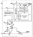
- semiconductor device
- cell group
- Prior art date
- Legal status (The legal status is an assumption and is not a legal conclusion. Google has not performed a legal analysis and makes no representation as to the accuracy of the status listed.)
- Pending
Links
- 239000004065 semiconductor Substances 0.000 title claims abstract description 28
- 230000005856 abnormality Effects 0.000 abstract description 19
- 230000002950 deficient Effects 0.000 abstract description 2
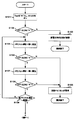
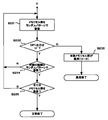
- 238000012360 testing method Methods 0.000 description 21
- 238000007689 inspection Methods 0.000 description 17
- 230000002159 abnormal effect Effects 0.000 description 15
- 238000000034 method Methods 0.000 description 12
- 238000010586 diagram Methods 0.000 description 11
- 230000008569 process Effects 0.000 description 10
- 238000012545 processing Methods 0.000 description 6
- 230000008859 change Effects 0.000 description 3
- 230000007423 decrease Effects 0.000 description 3
- 238000012544 monitoring process Methods 0.000 description 3
- 230000002093 peripheral effect Effects 0.000 description 3
- 102100031024 CCR4-NOT transcription complex subunit 1 Human genes 0.000 description 2
- 102100031025 CCR4-NOT transcription complex subunit 2 Human genes 0.000 description 2
- 101000919674 Caenorhabditis elegans CCR4-NOT transcription complex subunit let-711 Proteins 0.000 description 2
- 101001092183 Drosophila melanogaster Regulator of gene activity Proteins 0.000 description 2
- 101000919672 Homo sapiens CCR4-NOT transcription complex subunit 1 Proteins 0.000 description 2
- 101000919667 Homo sapiens CCR4-NOT transcription complex subunit 2 Proteins 0.000 description 2
- 238000000605 extraction Methods 0.000 description 2
- 230000006866 deterioration Effects 0.000 description 1
- 230000000694 effects Effects 0.000 description 1
- 230000006870 function Effects 0.000 description 1
- 230000004048 modification Effects 0.000 description 1
- 238000012986 modification Methods 0.000 description 1
- 230000008439 repair process Effects 0.000 description 1
- 230000002441 reversible effect Effects 0.000 description 1
Images


Landscapes
- Read Only Memory (AREA)
- For Increasing The Reliability Of Semiconductor Memories (AREA)
Priority Applications (1)
| Application Number | Priority Date | Filing Date | Title |
|---|---|---|---|
| JP2002175531A JP2004022067A (ja) | 2002-06-17 | 2002-06-17 | 半導体装置 |
Applications Claiming Priority (1)
| Application Number | Priority Date | Filing Date | Title |
|---|---|---|---|
| JP2002175531A JP2004022067A (ja) | 2002-06-17 | 2002-06-17 | 半導体装置 |
Publications (2)
| Publication Number | Publication Date |
|---|---|
| JP2004022067A true JP2004022067A (ja) | 2004-01-22 |
| JP2004022067A5 JP2004022067A5 (enExample) | 2005-09-15 |
Family
ID=31174153
Family Applications (1)
| Application Number | Title | Priority Date | Filing Date |
|---|---|---|---|
| JP2002175531A Pending JP2004022067A (ja) | 2002-06-17 | 2002-06-17 | 半導体装置 |
Country Status (1)
| Country | Link |
|---|---|
| JP (1) | JP2004022067A (enExample) |
Cited By (4)
| Publication number | Priority date | Publication date | Assignee | Title |
|---|---|---|---|---|
| KR100638461B1 (ko) * | 2004-12-30 | 2006-10-24 | 매그나칩 반도체 유한회사 | 플래시 메모리에서의 전하 펌핑 장치 및 방법 |
| JP2009245573A (ja) * | 2001-01-03 | 2009-10-22 | Samsung Electronics Co Ltd | 外部ピンを通じてワードライン電圧を出力する半導体メモリ装置及びその電圧測定方法 |
| JP2017174485A (ja) * | 2016-03-25 | 2017-09-28 | ローム株式会社 | 半導体記憶装置 |
| JP2022173138A (ja) * | 2021-05-06 | 2022-11-17 | インフィニオン テクノロジーズ アクチエンゲゼルシャフト | 電源・デジタル制御ループ |
-
2002
- 2002-06-17 JP JP2002175531A patent/JP2004022067A/ja active Pending
Cited By (5)
| Publication number | Priority date | Publication date | Assignee | Title |
|---|---|---|---|---|
| JP2009245573A (ja) * | 2001-01-03 | 2009-10-22 | Samsung Electronics Co Ltd | 外部ピンを通じてワードライン電圧を出力する半導体メモリ装置及びその電圧測定方法 |
| KR100638461B1 (ko) * | 2004-12-30 | 2006-10-24 | 매그나칩 반도체 유한회사 | 플래시 메모리에서의 전하 펌핑 장치 및 방법 |
| JP2017174485A (ja) * | 2016-03-25 | 2017-09-28 | ローム株式会社 | 半導体記憶装置 |
| JP2022173138A (ja) * | 2021-05-06 | 2022-11-17 | インフィニオン テクノロジーズ アクチエンゲゼルシャフト | 電源・デジタル制御ループ |
| JP7392032B2 (ja) | 2021-05-06 | 2023-12-05 | インフィニオン テクノロジーズ アクチエンゲゼルシャフト | 電源・デジタル制御ループ |
Similar Documents
| Publication | Publication Date | Title |
|---|---|---|
| US5351214A (en) | Memory with on-chip detection of bit line leaks | |
| JP4129170B2 (ja) | 半導体記憶装置及びメモリセルの記憶データ補正方法 | |
| EP0753859B1 (en) | Method for setting the threshold voltage of a reference memory cell | |
| US7920428B2 (en) | Methods and apparatuses relating to automatic cell threshold voltage measurement | |
| US20120008410A1 (en) | Detection of Word-Line Leakage in Memory Arrays: Current Based Approach | |
| EP0239968A2 (en) | Nonvolatile semiconductor memory device | |
| KR20040048870A (ko) | 반도체 기억장치 및 레퍼런스 셀의 보정방법 | |
| JPH07105159B2 (ja) | 半導体記憶装置の冗長回路 | |
| EP2487689A1 (en) | Digital method to obtain the I-V curves of NVM bitcells | |
| US20130308402A1 (en) | Test flow to detect a latent leaky bit of a non-volatile memory | |
| JPH097380A (ja) | 不揮発性半導体記憶装置 | |
| KR100558188B1 (ko) | 비휘발성 반도체 기억장치 및 행라인 단락 불량 검출방법 | |
| JP6502538B1 (ja) | 半導体記憶装置および解析システム | |
| JPH11328987A (ja) | 不揮発性半導体記憶装置 | |
| US7564714B2 (en) | Flash memory device and method of controlling program voltage | |
| KR20000023501A (ko) | 비휘발성 메모리 장치 및 그의 검사 방법 | |
| US7483305B2 (en) | Method, apparatus and system relating to automatic cell threshold voltage measurement | |
| JP3267301B2 (ja) | 検査回路を有する回路装置 | |
| KR19980071781A (ko) | 모든 메모리셀에 대해 소거 베리파이 동작이 일괄적으로 정확히 행해질 수 있는 반도체기억장치 | |
| KR20000057098A (ko) | 플래시 메모리 및 그 시험 방법 | |
| JP2004022067A (ja) | 半導体装置 | |
| US20150206594A1 (en) | Fuse circuit with test mode | |
| JP3588553B2 (ja) | 不揮発性半導体メモリ | |
| JP3346850B2 (ja) | 不揮発性半導体メモリ | |
| JP2008052841A (ja) | 自動セル閾値電圧測定に関する方法、装置及びシステム |
Legal Events
| Date | Code | Title | Description |
|---|---|---|---|
| A521 | Written amendment |
Free format text: JAPANESE INTERMEDIATE CODE: A523 Effective date: 20050216 |
|
| A621 | Written request for application examination |
Free format text: JAPANESE INTERMEDIATE CODE: A621 Effective date: 20050218 |
|
| A521 | Written amendment |
Free format text: JAPANESE INTERMEDIATE CODE: A523 Effective date: 20050401 |
|
| A977 | Report on retrieval |
Free format text: JAPANESE INTERMEDIATE CODE: A971007 Effective date: 20070620 |
|
| A131 | Notification of reasons for refusal |
Free format text: JAPANESE INTERMEDIATE CODE: A131 Effective date: 20070703 |
|
| A02 | Decision of refusal |
Free format text: JAPANESE INTERMEDIATE CODE: A02 Effective date: 20071030 |