JP2004022067A - Semiconductor device - Google Patents
Semiconductor device Download PDFInfo
- Publication number
- JP2004022067A JP2004022067A JP2002175531A JP2002175531A JP2004022067A JP 2004022067 A JP2004022067 A JP 2004022067A JP 2002175531 A JP2002175531 A JP 2002175531A JP 2002175531 A JP2002175531 A JP 2002175531A JP 2004022067 A JP2004022067 A JP 2004022067A
- Authority
- JP
- Japan
- Prior art keywords
- high voltage
- voltage
- memory cell
- semiconductor device
- cell group
- Prior art date
- Legal status (The legal status is an assumption and is not a legal conclusion. Google has not performed a legal analysis and makes no representation as to the accuracy of the status listed.)
- Pending
Links
Images


Abstract
Description
【0001】
【発明の属する技術分野】
本発明は、高電圧発生回路を有する半導体装置、特に高電圧発生回路及び発生された高電圧が供給されるEEPROMなど不揮発性メモリを有する半導体装置に関する。
【0002】
【従来の技術】
電気的プログラム可能なEEPROMなどの不揮発性メモリでは、データ書き換え時の電圧として、それが作り込まれる半導体装置の電源電圧(例えば、3V)より高い電圧(例えば、16V)を必要とする。通常、この高電圧は、その半導体装置に設けられる高電圧発生回路により、電源電圧を昇圧して得ている。
【0003】
従来、この高電圧発生回路からの高電圧は、その電圧値を単独で検査することはなく、不揮発性メモリのメモリセルが指令通りに書き込み及び消去できるかどうかの検査で代用されていた。このため、その検査結果が良或いは不良として得られても、不良である場合に、それが高電圧発生回路の異常によるものか、メモリセルの異常によるものかは、判定できていない。
【0004】
また、不揮発性メモリの検査では、一般的に、所定範囲のメモリセル群を単位として順次検査が行われるが、その際、当該メモリセル群を一律に全て消去‘1’或いは書き込み‘0’(1ワード16ビットの場合に、0(H)或いはF(H)、に相当する)を行って、その消去・書き込みの結果を判定することが多い。また、メモリセル群の検査を、一律に行うのでなく、組み合わせに応じて時間は長く掛かるがランダムに行うこともあった。
【0005】
【発明が解決しようとする課題】
しかし、所定のメモリセル群を一律に消去或いは書き込みする場合には、このメモリセル群内のメモリセルや、デコーダなどの周辺回路の対応する箇所においても印加される電圧が同時に変化することになる。従って、メモリセル間や対応する箇所間で、例えばリーク箇所等が存在したとしても、この検査においてはそれを検知することができないという問題がある。
【0006】
また、所定のメモリセル群をランダムに消去或いは書き込みする場合には、メモリセル間や対応する箇所間に存在するリーク箇所で、実際にリークが発生するが、そのリークの程度によっては、結果として指令通りに消去或いは書き込みが行われることがある。しかし、このような場合には、例え指令通りに消去或いは書き込みが行われたとしても、メモリセルのスレッショルド値Vthが予定されている値(例えば、0V→5V)に変化していない場合も多く、市場へ出荷後の故障発生の原因ともなっていた。
【0007】
そこで、本発明は、高電圧発生回路側の異常か不揮発性メモリ側の異常かを判別するとともに、不揮発性メモリ内部のリークなどの不具合な状態を検出することを可能にした、半導体装置を提供することを目的とする。
【0008】
【課題を解決するための手段】
請求項1の半導体装置は、メモリセルアレイ、デコーダを含み、データ書き換え時に高電圧を使用する不揮発性メモリ手段と、電源電圧を昇圧して前記高電圧を発生し、前記不揮発性メモリ手段に供給する高電圧発生手段と、前記不揮発性メモリ手段に供給される高電圧に応じた電圧を所定の電圧と比較する電圧判定手段とを、備えることを特徴とする。
【0009】
本発明によれば、不揮発性メモリ手段に供給される高電圧の電圧値を判定するから、半導体装置の検査時に、高電圧発生手段側と不揮発性メモリ手段側とを切り分けて検査することにより、発生した異常が、高電圧発生手段側の異常であるか或いは不揮発性メモリ手段側の異常であるかを区別して判定することができる。
【0010】
また、所定のメモリセル群をランダムに書き換えしながら、不揮発性メモリ手段に供給される高電圧の電圧値を判定することにより、書き換え結果に関わりなく、不揮発性メモリ手段側のリークの発生を検出することができる。
【0011】
また、発生された高電圧を外部に出力する必要がないので、そのための外部端子は不要であり、また高電圧発生手段の能力を本来の必要な分以上に上げる必要がない。
【0012】
【発明の実施の形態】
以下、図面を参照して、本発明の高電圧発生回路を有する半導体装置の実施の形態について説明する。
【0013】
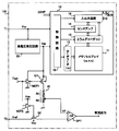
図1は、本発明の第1の実施の形態に係る半導体装置100の全体構成図であり、また、図2及び図3は、その動作フローを示す図である。
【0014】
図1において、半導体装置100の外部端子T1から電源電圧Vcc(例えば3V)が供給される。高電圧発生回路20は、チャージポンプ回路等の昇圧回路を備えており、供給される電源電圧Vccを昇圧して所定の高電圧Vpp(例えば16V)を発生する。
【0015】
不揮発性メモリ10は、EEPROMやフラッシュメモリ等であり、電源電圧Vccと高電圧Vppが供給されるとともに、検査信号を含む各種の制御信号CONTが供給される。不揮発性メモリ10には、メモリセルをm行n列に並べたメモリセルアレイ11、行を選択するローデコーダ12、列を選択するカラムデコーダ13、データを検出するセンスアンプ14、データを入出力する入出力回路15、これらを制御するための制御回路16等を含んでいる。
【0016】
このメモリセルアレイ11の消去、書き込み、読み出しの制御は、ローデコーダ12とカラムデコーダ13で指定される所定のメモリセル群毎に行われる。その消去や書き込み、即ち書き換え時に、高電圧Vppがメモリセルアレイ11やローデコーダ12、カラムデコーダ13等に印加されることになる。
【0017】
本発明では、高電圧発生回路20で発生され、不揮発性メモリ10に供給される高電圧Vppを、検査(或いは監視)してその電圧値を判定するための電圧判定手段を設けている。
【0018】
この電圧判定手段は、高電圧Vppとグランド間に、抵抗値R1と抵抗値R2に分圧する抵抗分圧器30と、動作しないときに抵抗分圧器30により消費電流が生じるのを防止するためのP型MOSトランジスタQ1が設けられる。これにより、以降の回路を通常の電源電圧Vccで動作させることができる。この抵抗分圧器30から取り出された分圧電圧Vpが比較器OP1の一方入力(+)に入力される。また、外部端子T2に供給される基準電圧VrefがP型MOSトランジスタQ2を介して、比較器OP1の他方入力(−)に入力される。トランジスタQ1、Q2のゲートにそれぞれ反転回路NOT1、NOT2を介して検査信号Testが印加される。なお、反転回路NOT1はレベルシフト回路を兼ねている。また、トランジスタQ1、Q2はアナログスイッチでも構わない。さらに、検査信号Testにより比較器OP1の動作を制御するようにしても良い。
【0019】
検査信号TestがHレベルになると、トランジスタQ1、Q2がオンし、比較器OP1には分圧電圧Vpと基準電圧Vrefとが入力される。分圧電圧Vpは、Vpp×R2/(R1+R2)だから抵抗値R1を3MΩ、抵抗値R2を1MΩとすると、高電圧Vppが16V以上であることを検査するためには、基準電圧Vrefを4Vにすればよい。勿論、高電圧発生回路20からの高電圧Vppは、不揮発性メモリ10の駆動により若干低下するから、その低下分を余裕分として見込んで設定される。これにより、比較器OP1の判定出力は、高電圧Vppが16V以上の時にHレベルになり、16V未満の時にはLレベルになる。
【0020】
次に、このように構成された図1の半導体装置の検査動作を、図2及び図3のフロー図をも参照して説明する。
【0021】
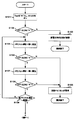
まず、図2で、テストを開始(スタート)すると、ステップS101で、検査信号TestをHレベルにし、Q1、Q2をオンする。この段階では、高電圧発生回路20の検査のみを目的としており、不揮発性メモリ10は駆動されていない。
【0022】
ステップS102で、分圧電圧Vpと基準電圧Vrefとが比較器OP1で比較される。比較器OP1の比較結果がLレベルの時には、高電圧発生回路20から所定の高電圧Vppが発生されていない。従って、ステップS103で高電圧発生回路20が異常であると判定し、異常終了する。この異常終了時には、比較器OP1からの判定出力Lレベルによって、テスト装置において警報、表示など所要の制御信号を発生させたり、不具合部のリペア動作を行うようにすればよい。一方、比較器OP1の比較結果がHレベルの時には、所定の高電圧Vppが高電圧発生回路20から発生されているから、不揮発性メモリ10の検査に移る。
【0023】
ステップS104で、順次、デコーダ12、13で指定される所定のメモリセル群のデータ内容を一律に消去する。
【0024】
この消去の結果、そのメモリセル群の各メモリセルが消去されたかどうかは、別途モニタされている。このモニタにより、消去されていないメモリセルが発見された場合には、そのメモリセル群は異常であると判定され、少なくともそのメモリセル群は使用されないように処置される。なお、異常であると判定されるメモリセル群には、そのメモリセル群自体及びそのメモリセル群に関係するデコーダなどの周辺回路も含まれる(以下、同様)。この一律の消去についてのモニタ及び処置については、一律の書き込みの場合、及びランダムの書き換えの場合にも、同様に適用される。
【0025】
ステップS105で、比較器OP1での比較結果がLレベルの時には、ステップS102で正常と判定されている高電圧発生回路20の高電圧が当該メモリセル群の駆動により低下したことになるから、ステップS106で当該メモリセル群は異常であると判定され、少なくともそのメモリセル群は使用されないように処置されて、異常終了する。
【0026】
なお、ステップS106で当該メモリセル群が異常であると判定された場合に、検査フローを終了するのでなく、その次のメモリセル群の検査に移るようにしても良い。このためには、ステップS106の異常判定後に、ステップS104に移るフローとすればよい。この異常判定後の処理フローは、他の異常判定ステップ(他の実施の形態を含む)においても同様に適用することができる。
【0027】
ステップS107で、ステップS104で一律消去されたメモリセル群を、一律に書き込む。そして、ステップS108で比較器OP1での比較結果がLレベルの時には、再びステップS106で当該メモリセル群は異常であると判定され、少なくともそのメモリセル群は使用されないように処置されて、異常終了する。
【0028】
ステップS108で、比較器OP1での比較結果がHレベルの時には、そのメモリセル群は一律書き換え(即ち、消去及び書き込み)の検査では正常と判定される。
【0029】
ステップS109で、全てのメモリセル群についてステップS104〜ステップS108の処理が行なわれたかどうかを判断し、全てのメモリセル群に対する一律書き換えの検査が終了したとき、図3のフロー図に移る。
【0030】
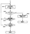
図3のフローでは、メモリセル群毎に所要の種類のランダムパターンで、書き換え(即ち、消去/書き込み)を行う。
【0031】
ステップS110で、あるメモリセル群を任意のランダムパターンで書き換える。
【0032】
このランダムパターンでの書き換えでは、一律の書き込みや消去の場合と異なり、隣り合うメモリセル間や対応する周辺回路の配線間でリークなどが発生している場合に、不揮発性メモリ10に供給されている高電圧Vppの電圧値が低下する。
【0033】
高電圧Vppの電圧値が低下した場合には、メモリセルの書き換え動作が完全には行われないことになる。もし、結果的に、書き換わったとしても、そのときのメモリセルのスレッショルド電圧Vthが正常時に0Vから5Vに書き変わるはずが、例えば0Vから3Vにしかならない、といった状態が発生する。
【0034】
従来であれば、この場合には、書き換え結果を別途モニタしていたとしても、結果的に、そのメモリセル群の各メモリセルが正常に書き換えられたと認識されてしまうから、そのようなリークを発見することはできない。
【0035】
本発明では、ステップS111で比較器OP1での比較結果を判定している。そして、その比較結果がLレベルの時には、ステップS112で当該メモリセル群はリークなどにより異常であると判定され、少なくともそのメモリセル群は使用されないように処置されて、異常終了する。
【0036】
そのメモリセル群について、ステップS113で、所要の種類のランダムパターンでの書き換えが行われたかどうかを判断し、所要の種類のランダムパターンでの書き換えの検査を実行する。
【0037】
ステップS114で、ステップS110〜S113の処理を全てのメモリセル群について行って、終了する。この場合は、高電圧発生回路20及び不揮発性メモリ10の両方が正常であると判定されたことになる。
【0038】
このように、不揮発性メモリ10に供給される高電圧Vppの電圧値を判定するから、半導体装置100の検査時に、高電圧発生回路20側と不揮発性メモリ10側とを切り分けて検査することにより、半導体装置100に発生した異常が、高電圧発生回路20側の異常であるか或いは不揮発性メモリ10側の異常であるかを区別して判定できる。
【0039】
また、所定のメモリセル群をランダムに書き換えしながら、不揮発性メモリ10に供給される高電圧Vppの電圧値を判定するから、各々のメモリセルの書き換え結果に関わりなく、不揮発性メモリ10内のリークの発生を検出できる。
【0040】
図4は、本発明の第2の実施の形態に係る半導体装置200の全体構成図であり、また、図5〜図7は、その動作フローを示す図である。
【0041】
図4において、半導体装置200は、図1の半導体装置と比較して、抵抗分圧器30がその分圧比を変更できる可変型となっていること、その分圧比を変化させるためのセレクタ40を設けていること、及び基準電圧Vrefを発生する基準電圧発生回路50を設けていること、検査信号Testによって基準電圧発生回路50及び比較器OP1を制御していることが、異なっている。また、トランジスタQ2及び反転回路NOT2が削除されている。その他の点は、図1と同様であるので、異なる点について説明する。
【0042】
抵抗分圧器30は、抵抗値R1、R2による分圧比を変えることができるように構成されている。このためには、例えば、多数の抵抗を直列に接続し、その多数の接続点から電圧取り出し用に配線を引き出し、それらの引出配線の1つから分圧電圧Vpを得るようにすればよい。
【0043】
セレクタ40は、抵抗分圧器30からの多数の引出配線のうちの1つを比較器OP1の入力端子に接続するように選択して、分圧電圧Vpを供給するように構成されている。具体的には、可逆シフトレジスタを用いて、比較器OP1の出力‘Hレベル’または‘Lレベル’により、上(右)シフトと、下(左)シフトを切り替えて、セレクト位置を任意の方向にシフトすることができる。どの引出配線の電圧を分圧電圧Vpとして選択するかは、比較器OP1の出力に応じてセレクタ40のセレクト位置を変化させることにより行う。また、そのセレクタ40の選択されたセレクト位置は、基準電圧Vrefとの関係で高電圧Vppの電圧値を表す(Vpp≒Vref×(R1+R2)/R2)から、このセレクト位置を出力してその時点での高電圧Vppの電圧値を得ることができるように構成される。
【0044】
また、基準電圧発生回路50は、半導体装置200の内部で基準電圧Vrefを発生させるもので、例えばバンドギャップ型定電圧回路を用いることにより、温度などに影響されにくい基準電圧を得ることができる。この場合、基準電圧Vref用の外部端子が不要となる。
【0045】
次に、このように構成された図4の半導体装置の検査動作を、図5〜図7のフロー図をも参照して説明する。
【0046】
まず、図5を参照して、スタートすると、ステップS201で、検査信号TestをHレベルにし、トランジスタQ1をオンするとともに、基準電圧発生回路50を制御して基準電圧Vrefを発生し、また比較器OP1を動作させる。この段階では、高電圧発生回路20の検査のみを目的としており、不揮発性メモリ10は駆動されていない。
【0047】
ステップS202で、選択されている分圧電圧Vpと基準電圧Vrefとが比較器OP1で比較される。
【0048】
ステップS202で比較器OP1の出力がHレベルの時は、高電圧Vppが高いのでどの程度の電圧値であるかを調べるために、ステップS203でセレクタ40のセレクト位置を1タップだけ下げる。そして、ステップS204で再び比較器OP1の出力を判定し、Hレベルの時にはさらにセレクタ40のセレクト位置を1タップだけ下げる。この処理を、ステップS204で比較器OP1の出力がLレベルになるまで繰り返す。Lレベルになると、ステップS205でセレクト位置を1タップ上げる。
【0049】
そして、ステップS206で、高電圧Vppの値をセレクト位置と基準電圧Vrefとに基づいて計算により求める。そして、求めた高電圧Vppが許容値以内かどうか判定する。高電圧Vppが許容値範囲外(この場合には予定値よりも高いことが検出される)の場合には、ステップS207で高電圧発生回路20が異常であると判定して、異常終了する。また、高電圧Vppが許容値範囲内の場合には、ステップS208で高電圧Vppの値を記憶する。
【0050】
一方、ステップS202で比較器OP1の出力がLレベルの時は、高電圧Vppが低いのでどの程度の電圧値であるかを調べるために、ステップS209でセレクタ40のセレクト位置を1タップだけ上げる。そして、ステップS210で再び比較器OP1の出力を判定し、Lレベルの時にはさらにセレクタ40のセレクト位置を1タップだけ下げる。この処理を、ステップS210で比較器OP1の出力がHレベルになるまで繰り返す。
【0051】
そして、ステップS211で、高電圧Vppの値をセレクト位置と基準電圧Vrefとに基づいて計算により求める。求めた高電圧Vppが許容値以内かどうか判定する。高電圧Vppが許容値範囲外(この場合には予定値よりも低いことが検出される)の場合には、ステップS207で高電圧発生回路20が異常であると判定して、異常終了する。また、高電圧Vppが許容値範囲内の場合には、ステップS208で高電圧Vppの値を記憶する。
【0052】
なお、セレクタ40のセレクト位置が最高の位置からスタートする場合には、図5のフロー中でステップS209〜S211は省略できる。また、逆に、セレクタ40のセレクト位置が最低の位置からスタートする場合には、図5のフロー中でステップS203〜S206は省略できる。
【0053】
この高電圧発生回路20単独での高電圧Vppの値が求められたら、図6のフロー図に移る。
【0054】
図6のフローでは、メモリセル群毎に一律の書き換え(即ち、消去及び書き込み)を行う。この図6のフローは、図2のステップS104〜ステップS109と同様である。各ステップを対応させると、ステップS220がステップS104に、ステップS221がステップS105に、ステップS222がステップS106に、ステップS223がステップS107に、ステップS224がステップS108に、ステップS225がステップS109になる。従って、ステップS225で全てのメモリセル群に対する一律書き換えの検査が終了したとき、図7のフロー図に移る。
【0055】
図7のフローでは、メモリセル群毎に所要の種類のランダムパターンで、書き換え(即ち、消去/書き込み)を行う。この図7のフローは、図3のステップS110〜ステップS114と同様である。各ステップを対応させると、ステップS231がステップS110に、ステップS232がステップS111に、ステップS233がステップS112に、ステップS234がステップS113に、ステップS235がステップS114になる。ステップS235で、全てのメモリセル群について行って終了すると、高電圧発生回路20及び不揮発性メモリ10の両方が正常であると判定されたことになる。
【0056】
図6、図7のフロー図においては、ステップS221、ステップS224及びステップS232において、比較器OP1での比較結果がLレベルの時には、直ちにステップS222及びステップS233で当該メモリセル群は異常であると判定している。
【0057】
しかし、この第2の実施の形態では、セレクタ40のセレクト位置に対応して分圧電圧Vpを変更できるから、高電圧Vppが低い場合にどの程度低いのかを判定することが可能である。この判定手法を、代表してステップS233について、図8のフロー図を参照して説明する。
【0058】
ステップS232で比較器OP1出力がLレベルになった場合を想定する。この場合には、まずステップS301でセレクタ40のセレクト位置を1タップ上げる。これによって、分圧電圧Vpは1タップ分だけ高くなるので、この状態でステップS302で再び比較器OP1の出力を判定する。
【0059】
このステップS302での判定がHレベルであれば、高電圧Vppの電圧低下は1タップ分以内であることが判明したので、この場合はメモリセル群は異常でないと判定することができる。
【0060】
ステップS302での判定でもLレベルであれば、高電圧Vppの電圧低下は大きいので、この場合はメモリセル群は異常である判定(S233)して、異常終了する。
【0061】
なお、どちらの判定になったとしても、次のメモリセル群の検査のために、ステップS303にて、セレクト位置を1タップ下げて元に戻しておくことが必要である。
【0062】
この図8の判定手法は、1タップに限らず、2タップ以上に亘って、採用することができる。また、この結果に基づいて、昇圧電圧である高電圧Vppを調整するようにしてもよい。
【0063】
このように、第2の実施の形態では、分圧器30を分圧比可変型とし、その分圧比を比較器OP1の出力により変更する。また、比較器OP1の出力により分圧器30の分圧比の変更操作を行うとともに、その変更された選択位置(即ち、セレクト位置)を出力するセレクタ40を設ける。これにより、分圧電圧Vpが基準電圧Vrefに合致するように、セレクタ40が分圧器30の分圧比を変更するから、そのセレクタ40の選択位置によって不揮発性メモリ10に供給される高電圧Vppの電圧値を知ることができる。従って、正常或いは異常の判定をより精度良く行うことができる。
【0064】
なお、各実施の形態において、検査信号Testが印加された場合に高電圧Vppを基準電圧Vrefと比較するようにしているが、この高電圧Vppの比較を常時行うようにしても良く、また定期的に行うようにしても良い。このように検査時以外にも高電圧Vppを監視することにより、実使用中の不揮発性メモリの劣化を検出することができる。
【0065】
【発明の効果】
本発明によれば、不揮発性メモリ手段に供給される高電圧の電圧値を判定するから、半導体装置の検査時に、高電圧発生手段側と不揮発性メモリ手段側とを切り分けて検査することにより、発生した異常が、高電圧発生手段側の異常であるか或いは不揮発性メモリ手段側の異常であるかを区別して判定することができる。
【0066】
また、所定のメモリセル群をランダムに書き換えしながら、不揮発性メモリ手段に供給される高電圧の電圧値を判定することにより、書き換え結果に関わりなく、不揮発性メモリ手段側のリークの発生を検出することができる。
【0067】
また、発生された高電圧を外部に出力する必要がないので、そのための外部端子は不要であり、また高電圧発生手段の能力を本来の必要な分以上に上げる必要がない。
【図面の簡単な説明】
【図1】本発明の第1の実施の形態に係る半導体装置の全体構成図。
【図2】図1の動作フローを示す図。
【図3】図1の動作フローを示す図。
【図4】本発明の第2の実施の形態に係る半導体装置の全体構成図。
【図5】図4の動作フローを示す図。
【図6】図4の動作フローを示す図。
【図7】図4の動作フローを示す図。
【図8】図6,図7の動作フローの変形を示す図。
【符号の説明】
100、200 半導体装置
10 不揮発性メモリ
11 メモリセルアレイ
12 ローデコーダ
13 カラムデコーダ
14 センスアンプ
15 入出力回路
16 制御回路
20 高電圧発生回路
30 抵抗分圧器
40 セレクタ
50 基準電圧発生回路
OP1 比較器
Q1、Q2 MOSトランジスタ
Vpp 高電圧
Vp 分圧電圧
Vref 基準電圧
Test 検査信号[0001]
TECHNICAL FIELD OF THE INVENTION
The present invention relates to a semiconductor device having a high voltage generating circuit, and more particularly to a semiconductor device having a high voltage generating circuit and a nonvolatile memory such as an EEPROM to which the generated high voltage is supplied.
[0002]
[Prior art]
2. Description of the Related Art A non-volatile memory such as an electrically programmable EEPROM requires a voltage (for example, 16 V) higher than a power supply voltage (for example, 3 V) of a semiconductor device in which the data is to be rewritten. Usually, this high voltage is obtained by boosting the power supply voltage by a high voltage generation circuit provided in the semiconductor device.
[0003]
Conventionally, the high voltage from this high voltage generating circuit has not been independently tested for its voltage value, but instead has been used for testing whether a memory cell of a nonvolatile memory can be programmed and erased as instructed. For this reason, even if the test result is obtained as good or bad, if the test result is bad, it cannot be determined whether it is due to an abnormality in the high voltage generation circuit or an abnormality in the memory cell.
[0004]
In general, in the inspection of the nonvolatile memory, the inspection is sequentially performed in units of a memory cell group within a predetermined range. At this time, all the memory cell groups are uniformly erased “1” or written “0” ( In the case of 1 word and 16 bits, 0 (H) or F (H) is performed), and the erase / write result is often determined. In addition, the inspection of the memory cell group is not performed uniformly, but may take a long time depending on the combination, but may be performed randomly.
[0005]
[Problems to be solved by the invention]
However, when a predetermined memory cell group is uniformly erased or written, the voltages applied to the memory cells in the memory cell group and the corresponding portions of peripheral circuits such as decoders simultaneously change. . Therefore, even if, for example, a leak location exists between the memory cells or between the corresponding locations, there is a problem that it cannot be detected in this inspection.
[0006]
In addition, when a predetermined memory cell group is randomly erased or written, a leak actually occurs at a leak location existing between memory cells or between corresponding locations. Erasing or writing may be performed as instructed. However, in such a case, even if erasing or writing is performed as instructed, the threshold value Vth of the memory cell often does not change to a predetermined value (for example, 0V → 5V). , Which was the cause of failure after shipment to the market.
[0007]
Therefore, the present invention provides a semiconductor device that can determine whether an abnormality is occurring on the high voltage generation circuit side or an abnormality on the non-volatile memory side and detect a faulty state such as a leak inside the non-volatile memory. The purpose is to do.
[0008]
[Means for Solving the Problems]
2. The semiconductor device according to
[0009]
According to the present invention, since the voltage value of the high voltage supplied to the nonvolatile memory means is determined, the semiconductor device is inspected by separating and inspecting the high voltage generation means side and the nonvolatile memory means side when inspecting the semiconductor device. It is possible to distinguish and determine whether the generated abnormality is an abnormality on the high voltage generation unit side or an abnormality on the nonvolatile memory unit side.
[0010]
Also, by determining the value of the high voltage supplied to the nonvolatile memory means while randomly rewriting a predetermined memory cell group, it is possible to detect the occurrence of a leak on the nonvolatile memory means side regardless of the rewriting result. can do.
[0011]
In addition, since it is not necessary to output the generated high voltage to the outside, an external terminal for the high voltage is not required, and the capability of the high voltage generating means does not need to be increased beyond the originally required amount.
[0012]
BEST MODE FOR CARRYING OUT THE INVENTION
Hereinafter, an embodiment of a semiconductor device having a high-voltage generation circuit according to the present invention will be described with reference to the drawings.
[0013]
FIG. 1 is an overall configuration diagram of a
[0014]
In FIG. 1, a power supply voltage Vcc (for example, 3 V) is supplied from an external terminal T1 of the
[0015]
The
[0016]
The control of erasing, writing, and reading of the
[0017]
In the present invention, there is provided a voltage determining means for inspecting (or monitoring) the high voltage Vpp generated by the high
[0018]
The voltage determining means includes a
[0019]
When the test signal Test goes high, the transistors Q1 and Q2 are turned on, and the divided voltage Vp and the reference voltage Vref are input to the comparator OP1. Since the divided voltage Vp is Vpp × R2 / (R1 + R2), if the resistance R1 is 3 MΩ and the resistance R2 is 1 MΩ, the reference voltage Vref is set to 4 V in order to check that the high voltage Vpp is 16 V or more. do it. Of course, since the high voltage Vpp from the high
[0020]
Next, the inspection operation of the semiconductor device of FIG. 1 configured as described above will be described with reference to the flowcharts of FIGS.
[0021]
First, in FIG. 2, when the test is started (started), in step S101, the inspection signal Test is set to the H level, and Q1 and Q2 are turned on. At this stage, the purpose is only to test the high
[0022]
In step S102, the divided voltage Vp and the reference voltage Vref are compared by the comparator OP1. When the comparison result of the comparator OP1 is at the L level, the predetermined high voltage Vpp has not been generated from the high
[0023]
In step S104, the data contents of a predetermined memory cell group specified by the
[0024]
Whether or not each memory cell of the memory cell group has been erased as a result of this erasure is separately monitored. When a memory cell that has not been erased is found by this monitor, the memory cell group is determined to be abnormal, and at least the memory cell group is treated so as not to be used. Note that the memory cell group determined to be abnormal includes the memory cell group itself and peripheral circuits such as a decoder related to the memory cell group (hereinafter the same). This uniform erasure monitoring and processing is similarly applied to uniform writing and random rewriting.
[0025]
If the comparison result of the comparator OP1 is at L level in step S105, it means that the high voltage of the high
[0026]
Note that when it is determined in step S106 that the memory cell group is abnormal, the inspection flow may not be terminated but the inspection of the next memory cell group may be performed. For this purpose, it is sufficient that the flow proceeds to step S104 after the abnormality is determined in step S106. The processing flow after the abnormality determination can be similarly applied to other abnormality determination steps (including other embodiments).
[0027]
In step S107, the memory cell group uniformly erased in step S104 is uniformly written. When the comparison result of the comparator OP1 is at the L level in step S108, the memory cell group is again determined to be abnormal in step S106, and at least the memory cell group is treated so as not to be used, and abnormal termination is performed. I do.
[0028]
In step S108, when the comparison result of the comparator OP1 is at the H level, the memory cell group is determined to be normal in the uniform rewrite (ie, erase and write) inspection.
[0029]
In step S109, it is determined whether or not the processing in steps S104 to S108 has been performed for all the memory cell groups. When the uniform rewrite inspection has been completed for all the memory cell groups, the flow shifts to the flowchart of FIG.
[0030]
In the flow of FIG. 3, rewriting (that is, erasing / writing) is performed with a required type of random pattern for each memory cell group.
[0031]
In step S110, a certain memory cell group is rewritten with an arbitrary random pattern.
[0032]
In the rewriting with the random pattern, unlike the case of uniform writing and erasing, when a leak or the like occurs between adjacent memory cells or wiring of a corresponding peripheral circuit, the data is supplied to the
[0033]
When the voltage value of the high voltage Vpp decreases, the rewriting operation of the memory cell is not completely performed. As a result, even if the data is rewritten, the threshold voltage Vth of the memory cell at that time should be rewritten from 0 V to 5 V when the memory cell is normal, but the state is changed from 0 V to 3 V, for example.
[0034]
Conventionally, in this case, even if the rewrite result is separately monitored, as a result, it is recognized that each memory cell of the memory cell group has been normally rewritten. It cannot be found.
[0035]
In the present invention, the comparison result of the comparator OP1 is determined in step S111. Then, when the comparison result is at the L level, it is determined in step S112 that the memory cell group is abnormal due to leakage or the like, and at least the memory cell group is treated so as not to be used, and the process ends abnormally.
[0036]
In step S113, it is determined whether or not the memory cell group has been rewritten with a required type of random pattern, and an inspection of rewriting with the required type of random pattern is performed.
[0037]
In step S114, the processes in steps S110 to S113 are performed for all the memory cell groups, and the process ends. In this case, it is determined that both the high
[0038]
As described above, since the voltage value of the high voltage Vpp supplied to the
[0039]
Further, since the voltage value of the high voltage Vpp supplied to the
[0040]
FIG. 4 is an overall configuration diagram of a
[0041]
4, the
[0042]
The
[0043]
The
[0044]
The reference
[0045]
Next, the inspection operation of the semiconductor device of FIG. 4 configured as described above will be described with reference to the flowcharts of FIGS.
[0046]
First, referring to FIG. 5, when started, in step S201, the inspection signal Test is set to the H level, the transistor Q1 is turned on, and the reference
[0047]
In step S202, the selected divided voltage Vp and the reference voltage Vref are compared by the comparator OP1.
[0048]
If the output of the comparator OP1 is at the H level in step S202, the select position of the
[0049]
Then, in step S206, the value of the high voltage Vpp is obtained by calculation based on the select position and the reference voltage Vref. Then, it is determined whether the obtained high voltage Vpp is within an allowable value. If the high voltage Vpp is outside the allowable value range (in this case, it is detected that it is higher than the predetermined value), it is determined in step S207 that the high
[0050]
On the other hand, when the output of the comparator OP1 is at the L level in step S202, the select position of the
[0051]
Then, in step S211, the value of the high voltage Vpp is obtained by calculation based on the select position and the reference voltage Vref. It is determined whether the obtained high voltage Vpp is within an allowable value. If the high voltage Vpp is out of the allowable value range (in this case, it is detected that it is lower than the predetermined value), it is determined in step S207 that the high
[0052]
When the selection position of the
[0053]
When the value of the high voltage Vpp in the high
[0054]
In the flow of FIG. 6, uniform rewriting (that is, erasing and writing) is performed for each memory cell group. The flow in FIG. 6 is the same as Steps S104 to S109 in FIG. When the steps correspond to each other, step S220 corresponds to step S104, step S221 corresponds to step S105, step S222 corresponds to step S106, step S223 corresponds to step S107, step S224 corresponds to step S108, and step S225 corresponds to step S109. Accordingly, when the uniform rewrite inspection for all the memory cell groups is completed in step S225, the process proceeds to the flowchart of FIG.
[0055]
In the flow of FIG. 7, rewriting (that is, erasing / writing) is performed with a required type of random pattern for each memory cell group. The flow of FIG. 7 is similar to steps S110 to S114 of FIG. When the steps correspond to each other, step S231 corresponds to step S110, step S232 corresponds to step S111, step S233 corresponds to step S112, step S234 corresponds to step S113, and step S235 corresponds to step S114. In step S235, when the processing is performed for all the memory cell groups and the processing is completed, it is determined that both the high
[0056]
In the flowcharts of FIGS. 6 and 7, when the comparison result of the comparator OP1 is at the L level in steps S221, S224, and S232, the memory cell group is immediately determined to be abnormal in steps S222 and S233. Has been determined.
[0057]
However, in the second embodiment, since the divided voltage Vp can be changed according to the selected position of the
[0058]
It is assumed that the output of the comparator OP1 becomes L level in step S232. In this case, first, in step S301, the select position of the
[0059]
If the determination in step S302 is at the H level, it has been found that the voltage drop of the high voltage Vpp is within one tap, and in this case, it can be determined that the memory cell group is not abnormal.
[0060]
If the determination in step S302 is also at the L level, the voltage drop of the high voltage Vpp is large. In this case, the memory cell group is determined to be abnormal (S233), and the process ends abnormally.
[0061]
Regardless of which judgment is made, it is necessary to lower the select position by one tap and return to the original position in step S303 in order to inspect the next memory cell group.
[0062]
The determination method of FIG. 8 is not limited to one tap, and can be adopted over two or more taps. Further, the high voltage Vpp, which is a boosted voltage, may be adjusted based on the result.
[0063]
As described above, in the second embodiment, the
[0064]
In each of the embodiments, when the test signal Test is applied, the high voltage Vpp is compared with the reference voltage Vref. However, the comparison of the high voltage Vpp may be performed at all times. You may make it perform it. As described above, by monitoring the high voltage Vpp other than at the time of the inspection, it is possible to detect the deterioration of the nonvolatile memory in actual use.
[0065]
【The invention's effect】
According to the present invention, since the voltage value of the high voltage supplied to the nonvolatile memory means is determined, the semiconductor device is inspected by separating and inspecting the high voltage generating means side and the nonvolatile memory means side when inspecting the semiconductor device. It is possible to distinguish and determine whether the generated abnormality is an abnormality on the high voltage generation unit side or an abnormality on the nonvolatile memory unit side.
[0066]
Also, by determining the value of the high voltage supplied to the nonvolatile memory means while randomly rewriting a predetermined memory cell group, it is possible to detect the occurrence of a leak on the nonvolatile memory means side regardless of the rewriting result. can do.
[0067]
In addition, since it is not necessary to output the generated high voltage to the outside, an external terminal for the high voltage is not required, and it is not necessary to increase the capability of the high voltage generating means beyond the originally required amount.
[Brief description of the drawings]
FIG. 1 is an overall configuration diagram of a semiconductor device according to a first embodiment of the present invention.
FIG. 2 is a diagram showing an operation flow of FIG. 1;
FIG. 3 is a diagram showing an operation flow of FIG. 1;
FIG. 4 is an overall configuration diagram of a semiconductor device according to a second embodiment of the present invention.
FIG. 5 is a diagram showing an operation flow of FIG. 4;
FIG. 6 is a diagram showing an operation flow of FIG. 4;
FIG. 7 is a view showing the operation flow of FIG. 4;
FIG. 8 is a diagram showing a modification of the operation flow of FIGS. 6 and 7;
[Explanation of symbols]
100, 200
Claims (1)
電源電圧を昇圧して前記高電圧を発生し、前記不揮発性メモリ手段に供給する高電圧発生手段と、
前記不揮発性メモリ手段に供給される高電圧に応じた電圧を所定の電圧と比較する電圧判定手段とを、備えることを特徴とする半導体装置。A nonvolatile memory means including a memory cell array and a decoder, and using a high voltage when rewriting data;
High voltage generating means for raising the power supply voltage to generate the high voltage and supplying the high voltage to the nonvolatile memory means;
A semiconductor device comprising: a voltage determination unit that compares a voltage corresponding to a high voltage supplied to the nonvolatile memory unit with a predetermined voltage.
Priority Applications (1)
| Application Number | Priority Date | Filing Date | Title |
|---|---|---|---|
| JP2002175531A JP2004022067A (en) | 2002-06-17 | 2002-06-17 | Semiconductor device |
Applications Claiming Priority (1)
| Application Number | Priority Date | Filing Date | Title |
|---|---|---|---|
| JP2002175531A JP2004022067A (en) | 2002-06-17 | 2002-06-17 | Semiconductor device |
Publications (2)
| Publication Number | Publication Date |
|---|---|
| JP2004022067A true JP2004022067A (en) | 2004-01-22 |
| JP2004022067A5 JP2004022067A5 (en) | 2005-09-15 |
Family
ID=31174153
Family Applications (1)
| Application Number | Title | Priority Date | Filing Date |
|---|---|---|---|
| JP2002175531A Pending JP2004022067A (en) | 2002-06-17 | 2002-06-17 | Semiconductor device |
Country Status (1)
| Country | Link |
|---|---|
| JP (1) | JP2004022067A (en) |
Cited By (3)
| Publication number | Priority date | Publication date | Assignee | Title |
|---|---|---|---|---|
| KR100638461B1 (en) * | 2004-12-30 | 2006-10-24 | 매그나칩 반도체 유한회사 | Charge pump device in flash memory |
| JP2009245573A (en) * | 2001-01-03 | 2009-10-22 | Samsung Electronics Co Ltd | Semiconductor memory device outputting word line voltage through external pin and voltage measurement method thereof |
| JP7392032B2 (en) | 2021-05-06 | 2023-12-05 | インフィニオン テクノロジーズ アクチエンゲゼルシャフト | Power supply/digital control loop |
-
2002
- 2002-06-17 JP JP2002175531A patent/JP2004022067A/en active Pending
Cited By (3)
| Publication number | Priority date | Publication date | Assignee | Title |
|---|---|---|---|---|
| JP2009245573A (en) * | 2001-01-03 | 2009-10-22 | Samsung Electronics Co Ltd | Semiconductor memory device outputting word line voltage through external pin and voltage measurement method thereof |
| KR100638461B1 (en) * | 2004-12-30 | 2006-10-24 | 매그나칩 반도체 유한회사 | Charge pump device in flash memory |
| JP7392032B2 (en) | 2021-05-06 | 2023-12-05 | インフィニオン テクノロジーズ アクチエンゲゼルシャフト | Power supply/digital control loop |
Similar Documents
| Publication | Publication Date | Title |
|---|---|---|
| US5351214A (en) | Memory with on-chip detection of bit line leaks | |
| JP4129170B2 (en) | Semiconductor memory device and memory data correction method for memory cell | |
| EP0753859B1 (en) | Method for setting the threshold voltage of a reference memory cell | |
| US7920428B2 (en) | Methods and apparatuses relating to automatic cell threshold voltage measurement | |
| US20120008410A1 (en) | Detection of Word-Line Leakage in Memory Arrays: Current Based Approach | |
| US7483305B2 (en) | Method, apparatus and system relating to automatic cell threshold voltage measurement | |
| KR20040048870A (en) | Semiconductor memory device and method for correcting a reference cell | |
| JPH07105159B2 (en) | Redundant circuit of semiconductor memory device | |
| US8995202B2 (en) | Test flow to detect a latent leaky bit of a non-volatile memory | |
| KR100558188B1 (en) | Nonvolatile semiconductor storage device and row-line short defect detection method | |
| JPH097380A (en) | Nonvolatile semiconductor memory device | |
| EP2487689A1 (en) | Digital method to obtain the I-V curves of NVM bitcells | |
| JPH11328987A (en) | Nonvolatile semiconductor memory device | |
| US7564714B2 (en) | Flash memory device and method of controlling program voltage | |
| JP2001236792A (en) | Refresh method for fixed value memory, its refresh device, and digital control device | |
| CN101667455A (en) | Semiconductor memory device | |
| JP5486948B2 (en) | Nonvolatile semiconductor memory device having defect detection circuit and defect detection method of nonvolatile semiconductor memory device | |
| KR19980071781A (en) | A semiconductor memory device in which an erase verify operation can be performed in a lump accurately for all memory cells | |
| JP2004022067A (en) | Semiconductor device | |
| JP2008004264A (en) | Nonvolatile semiconductor memory device, and method for detecting and replacing bad column in the same | |
| JP2008052841A (en) | Method, device, and system concerning automatic cell threshold voltage measurement | |
| JP3267301B2 (en) | Circuit device having inspection circuit | |
| JP3588553B2 (en) | Non-volatile semiconductor memory | |
| JP3346850B2 (en) | Non-volatile semiconductor memory | |
| US6972994B2 (en) | Circuit and a method to screen for defects in an addressable line in a non-volatile memory |
Legal Events
| Date | Code | Title | Description |
|---|---|---|---|
| A521 | Written amendment |
Free format text: JAPANESE INTERMEDIATE CODE: A523 Effective date: 20050216 |
|
| A621 | Written request for application examination |
Free format text: JAPANESE INTERMEDIATE CODE: A621 Effective date: 20050218 |
|
| A521 | Written amendment |
Free format text: JAPANESE INTERMEDIATE CODE: A523 Effective date: 20050401 |
|
| A977 | Report on retrieval |
Free format text: JAPANESE INTERMEDIATE CODE: A971007 Effective date: 20070620 |
|
| A131 | Notification of reasons for refusal |
Free format text: JAPANESE INTERMEDIATE CODE: A131 Effective date: 20070703 |
|
| A02 | Decision of refusal |
Free format text: JAPANESE INTERMEDIATE CODE: A02 Effective date: 20071030 |