JP2004014672A - Substrate for semiconductor device and its manufacturing method - Google Patents
Substrate for semiconductor device and its manufacturing method Download PDFInfo
- Publication number
- JP2004014672A JP2004014672A JP2002163989A JP2002163989A JP2004014672A JP 2004014672 A JP2004014672 A JP 2004014672A JP 2002163989 A JP2002163989 A JP 2002163989A JP 2002163989 A JP2002163989 A JP 2002163989A JP 2004014672 A JP2004014672 A JP 2004014672A
- Authority
- JP
- Japan
- Prior art keywords
- wiring pattern
- conductor layer
- thin
- pattern
- resist pattern
- Prior art date
- Legal status (The legal status is an assumption and is not a legal conclusion. Google has not performed a legal analysis and makes no representation as to the accuracy of the status listed.)
- Pending
Links
Images


Abstract
Description
【0001】
【発明の属する技術分野】
半導体素子と外部基板を接続する際の接続媒体となるもので、高放熱性と微細回路配線を有する半導体装置用基板とその製造方法に関する。
【0002】
【従来の技術】
ポリイミド、ガラスエポキシ等の絶縁基材上に配線パターンを形成する方法としては、均一厚の銅箔をラミネートし導体層を形成し、この導体層に液体レジストをコーティングして感光層を形成し、パターン露光、現像等のフォトリソ工程によりレジストパターンを形成し、レジストパターンをマスクにして導体層をエッチングして所定の配線パターンを形成するサブトラクティブ法が一般的である。
【0003】
また、ポリイミド、ガラスエポキシなどの絶縁基材上に配線パターンを形成する別の方法として、まず、無電解めっき等で形成した薄膜導体層上にドライフィルムレジストをラミネートしフォトリソ工程を行いめっき用のレジストパターンを形成し、レジストパターン以外の領域に電解めっき等で所定厚の導体層を形成し、レジストパターンを剥離処理し、フラッシュエッチングにて薄膜導体層を除去し、所定の配線パターンを形成するセミアディティブ法がある。
【0004】
上記いずれの方法においても、配線パターンの導体膜厚は絶縁基材上のいずれの場所でも同じである。
【0005】
【発明が解決しようとする課題】
配線パターンのファインピッチ化に対応するため、アディティブ法では導体層膜厚の薄型化、セミアディティブ法ではファインパターンを形成するための感光層の薄型化、結果として配線パターンの薄型化の傾向にある。
例えば、50μm以下のファインピッチの配線パターンを形成する場合、配線パターンの膜厚は薄くなるが、配線パターンの膜厚が薄くなることで配線強度の弱体化、放熱性の減少など信頼性低下を招く可能性がでており、配線パターンの種類、機能、特性等により配線パターンの膜厚を区分けする必要性が生じていた。
【0006】
本発明は上記必要性に鑑み考案されたもので、信頼性を維持しながら、配線パターンの微細化、高密度化に対応できる半導体装置用基板及びその製造方法を提供することを目的とする。
【0007】
【課題を解決するための手段】
本発明に於いて上記課題を達成するため、まず請求項1においては、絶縁基材上の片面もしくは両面に配線パターンが形成された半導体装置用基板であって、前記配線パターンが薄い導体からなる薄配線パターンと厚い導体からなる厚配線パターンとで形成されていることを特徴とする半導体装置用基板としたものである。
【0008】
また、請求項2においては、前記薄配線パターンは配線ピッチが50μm以下で、前記厚配線パターンは配線ピッチが50μm以上で形成されていることを特徴とする請求項1記載の半導体装置用基板としたものである。
【0009】
また、請求項3においては、前記厚配線パターンの導体厚みは前記薄配線パターンの導体厚みの2倍以上になっていることを特徴とする請求項1または2に記載の半導体装置用基板としたものである。
【0010】
また、請求項4においては、少なくとも以下の工程を備えていることを特徴とする請求項1乃至3のいずれか一項に記載の半導体装置用基板の製造方法としたものである。
(a)絶縁基材の片面もしくは両面に薄膜導体層を形成する工程。
(b)薄膜導体層上にレジストパターンを形成する工程。
(c)レジストパターンをマスクにして電解銅めっき等を行い、薄膜導体層上の開口部に所定厚の導体層を形成する工程。
(d)レジストパターンを剥離処理し、薄配線パターン用導体層を形成する工程。
(e)薄膜導体層及び薄配線パターン用導体層上に所定厚の感光層を形成する工程。
(f)感光層をパターニング処理し、所定の薄配線パターン用導体層上に開口部を有するレジストパターンを形成する工程。
(g)レジストパターンをマスクにして電解銅めっき等を行い、薄配線パターン用導体層上の開口部に嵩上げ用導体層を形成する工程。
(h)レジストパターンを剥離処理し、レジストパターン下部にあった薄膜導体層をフラッシュエッチングにて除去し、薄配線パターン及び厚配線パターンを形成する工程。
【0011】
また、請求項5においては、少なくとも以下の工程を備えていることを特徴とする請求項1乃至3のいずれか一項に記載の半導体装置用基板の製造方法としたものである。
(a)絶縁基材の片面もしくは両面に薄膜導体層を形成する工程。
(b)薄膜導体層上にレジストパターンを形成する工程。
(c)レジストパターンをマスクにして電解銅めっき等を行い、薄膜導体層上の開口部に所定厚の導体層を形成する工程。
(d)レジストパターンを剥離処理し、薄配線パターン用導体層を形成する工程。
(e)薄膜導体層及び薄配線パターン用導体層上に所定厚の感光層を形成する工程。
(f)感光層をパターニング処理し、薄膜導体層上に開口部を有するレジストパターンを形成する工程。
(g)レジストパターンをマスクにして電解銅めっき等を行い、薄配線パターン用導体層上の開口部に厚配線パターン用導体層を形成する工程。
(h)レジストパターンを剥離処理し、レジストパターン下部にあった薄膜導体層をフラッシュエッチングにて除去し、薄配線パターン及び厚配線パターンを形成する工程。
【0012】
また、請求項6においては、少なくとも以下の工程を備えていることを特徴とする請求項1乃至3のいずれか一項に記載の半導体装置用基板の製造方法としたものである。
(a)絶縁基材の片面もしくは両面に所定厚の薄配線パターン用導体層を形成する工程。
(b)薄配線パターン用導体層上にレジストパターンを形成する工程。
(c)レジストパターンをマスクにして薄配線パターン用導体層をエッチングする工程。
(d)レジストパターンを剥離処理し、薄配線パターンを形成する工程。
(e)絶縁基材及び薄配線パターン上に所定厚の感光層を形成する工程。
(f)感光層をパターニング処理し、所定の薄配線パターン上に開口部を有するレジストパターンを形成する工程。
(g)レジストパターンをマスクにして電解銅めっき等を行い、薄配線パターン上の開口部に嵩上げ用導体層を形成する工程。
(h)レジストパターンを剥離処理し、薄配線パターン及び厚配線パターンを形成する工程。
【0013】
さらにまた、請求項7においては、少なくとも以下の工程を備えていることを特徴とする請求項1乃至3のいずれか一項に記載の半導体装置用基板の製造方法としたものである。
(a)絶縁基材の片面もしくは両面に所定厚の薄配線パターン用導体層を形成する工程。
(b)薄配線パターン用導体層上にレジストパターンを形成する工程。
(c)レジストパターンをマスクにして薄配線パターン用導体層をエッチングする工程。
(d)レジストパターンを剥離処理し、薄配線パターン及び絶縁基材の所定位置にビア用孔を形成する工程。
(e)絶縁基材及び薄配線パターン上に所定厚の感光層を形成する工程。
(f)感光層をパターニング処理し、所定の薄配線パターン上及びビア用孔上に開口部を有するレジストパターンを形成する工程。
(g)レジストパターンをマスクにして電解銅めっき等を行い、薄配線パターン上の開口部に嵩上げ用導体層を、ビア用孔にフィルドビア及び配線用導体層を形成する工程。
(h)レジストパターンを剥離し、薄配線パターン、厚配線パターン及びビア接続された配線パターンを形成する工程。
【0014】
【発明の実施の形態】
以下本発明の実施の形態につき説明する。
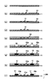
図1(a)〜(d)に、本発明の半導体装置用基板の実施例のいくつかを示す。請求項1に係る半導体装置用基板は同一基板上に薄配線パターンと厚配線パターンを混在させ、配線パターンの種類、機能等によって、薄配線パターンと厚配線パターンとに振り分けを行おうというものである。
例えば、高密度、高精度の配線パターンは薄配線パターンに、高放熱特性で且つ粗い配線パターンの場合は厚配線パターンにする。
【0015】
請求項2に係る発明は、薄配線パターンと厚配線パターンとの振り分けを配線パターンピッチによって行うもので、配線ピッチが50μm以上を厚配線パターン、配線ピッチが50μm以下を薄配線パターンとすることにより、上記の配線パターンの機能、特性を満たすことができる。
【0016】
請求項3に係る発明は、薄配線パターンと厚配線パターンとの振り分けを配線パターンの膜厚によって行うもので、厚配線パターンの膜厚を、薄配線パターンの膜厚の2倍以上にすることにより、高放熱特性を持たせることができる。
【0017】
以下本発明の半導体装置用基板の製造法について述べる。
請求項4に係る半導体装置用基板の製造方法は、薄配線パターンをセミアディティブ法で作製し、薄配線パターンに嵩上げ導体層を積み上げて厚配線パターンを作製する方法である。
まず、ダイレクトプレーティングシステム(以下、DPSと称す)等により、絶縁基材11表面に導電層を形成し、電解銅めっきにより薄膜導体層(特に図示せず)を形成する(図2(a)参照)。
次に、感光性レジストを塗布するか、ドライフィルムをラミネートする等の方法で感光層を形成し、パターン露光、現像等の一連のパターニング処理を行ってレジストパターン21を形成する(図2(b)参照)。
【0018】
次に、レジストパターン21をめっきマスクにして電解銅めっきを行い、薄膜導体層上に導体層31及び32を形成する(図2(c)参照)。
次に、レジストパターンを専用の剥離液で剥離処理し、配線ピッチ50μm以下の薄配線パターン用導体層31及び配線ピッチ50μm以上の薄配線パターン用導体層32を形成する(図2(d)参照)。
次に、ドライフィルムをラミネートする等の方法で所定厚の感光層22を形成し(図2(e)参照)、パターン露光、現像等の一連のパターニング処理を行って、配線ピッチ50μm以上の薄配線パターン用導体層32上に開口部41を有するレジストパターン22aを形成する(図2(f)参照)。
【0019】
次に、レジストパターン22aをめっきマスクにして電解銅めっき等を行い、薄配線パターン用導体層32上の開口部41に嵩上げ用導体層33を形成する(図2(g)参照)。
次に、嵩上げ用導体層33上にAuめっき皮膜51を形成し(図2(h)参照)、レジストパターン22aを専用の剥離液で剥離処理して、レジストパターン22a下部にあった薄膜導体層をフラッシュエッチングで除去し、絶縁基材11上に配線ピッチ50μm以下の薄配線パターン31a及び薄配線パターン32aと嵩上げ用導体層33とからなる配線ピッチ50μm以上の厚配線パターン34が形成された半導体装置用基板100を得る(図2(i)参照)。
ここで、Auめっき皮膜51は半田及びボンディング用の下地層として形成するもので、省略する場合もある。
【0020】
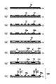
請求項5に係る半導体装置用基板の製造方法は、薄配線パターン及び厚配線パターンをセミアディティブ法で作製する方法である。
まず、DPS工程等により、絶縁基材11表面に導電層を形成し、電解銅めっきにより銅皮膜からなる薄膜導体層(特に図示せず)を形成する(図3(a)参照)。
次に、感光性レジストを塗布するか、ドライフィルムをラミネートする等の方法で感光層を形成し、パターン露光、現像等の一連のパターニング処理を行ってレジストパターン21を形成する(図3(b)参照)。
【0021】
次に、レジストパターン21をめっきマスクにして電解銅めっきを行い、薄膜導体層上に導体層31を形成する(図3(c)参照)。
次に、レジストパターン21を専用の剥離液で剥離処理し、配線ピッチ50μm以下の薄配線パターン用導体層31を形成する(図3(d)参照)。
次に、ドライフィルムをラミネートする等の方法で所定厚の感光層22を形成し(図3(e)参照)、パターン露光、現像等の一連のパターニング処理を行って、絶縁基材11の薄膜導体層上の所定位置に開口部42を有するレジストパターン22aを形成する(図3(f)参照)。
【0022】
次に、レジストパターン22aをめっきマスクにして電解銅めっき等を行い、薄膜導体層上の開口部42に厚配線パターン用導体層35を形成する(図3(g)参照)。
次に、厚配線パターン用導体層35上にAuめっき皮膜51を形成し(図3(h)参照)、レジストパターン22aを専用の剥離液で剥離処理して、レジストパターン22a下部にあった薄膜導体層をフラッシュエッチングで除去し、絶縁基材11上に配線ピッチ50μm以下の薄配線パターン31a及び配線ピッチ50μm以上の厚配線パターン35aが形成された半導体装置用基板200を得る(図3(i)参照)。
ここで、Auめっき皮膜51は半田及びボンディング用の下地層として形成するもので、省略する場合もある。
【0023】
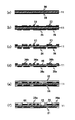
請求項6に係る半導体装置用基板の製造方法は、薄配線パターンをサブトラクティブ法で作製し、薄配線パターンに嵩上げ導体層を積み上げて厚配線パターンを作製する方法である。
まず、絶縁基材11上に所定厚の銅箔等を貼り合わせて導体層36を形成する(図4(a)参照)。
ここで、導体層36の膜厚は薄配線パターンの膜厚に設定する。
次に、感光性レジストを塗布するか、ドライフィルムをラミネートする等の方法で感光層を形成し、パターン露光、現像等の一連のパターニング処理を行ってレジストパターン21を形成する(図4(b)参照)。
【0024】
次に、レジストパターン21をエッチングマスクにして導体層36をエッチングして(図4(c)参照)、レジストパターン21を専用の剥離液で剥離処理して配線ピッチ50μm以下の薄配線パターン36a及び配線ピッチ50μm以上の薄配線パターン36bを形成する(図4(d)参照)。
次に、ドライフィルムをラミネートする等の方法で所定厚の感光層22を形成し(図4(e)参照)、パターン露光、現像等の一連のパターニング処理を行って、配線ピッチ50μm以上の薄配線パターン36b上に開口部41を有するレジストパターン22aを形成する(図4(f)参照)。
【0025】
次に、レジストパターン22aをめっきマスクにして電解銅めっき等を行い、薄配線パターン36b上の開口部41に嵩上げ用導体層33を形成する(図4(g)参照)。
次に、レジストパターン22aを専用の剥離液で剥離処理し、絶縁基材11上に配線ピッチ50μm以下の薄配線パターン36a及び薄配線パターン36bと嵩上げ用導体層33とからなる配線ピッチ50μm以上の厚配線パターン34が形成された半導体装置用基板300を得る(図4(h)参照)。
【0026】
請求項7に係る半導体装置用基板の製造方法は、薄配線パターンをサブトラクティブ法で作製し、薄配線パターンに嵩上げ導体層を積み上げて厚配線パターンを、嵩上げ導体層作成時にフィルドビア及び配線パターン用導体層を同時に作製する方法である。
まず、絶縁基材11の両面に所定厚の銅箔等を貼り合わせて導体層36を形成する(図5(a)参照)。
ここで、導体層36の膜厚は薄配線パターンの層厚に設定する。
次に、感光性レジストを塗布するか、ドライフィルムをラミネートする等の方法で感光層を形成し、パターン露光、現像等の一連のパターニング処理を行ってレジストパターン23及び24を形成する(図5(b)参照)。
【0027】
次に、レジストパターン23及び24をエッチングマスクにして導体層36をエッチングし(図5(c)参照)、レジストパターン23及び24を専用の剥離液で剥離処理して配線ピッチ50μm以下の薄配線パターン36a及び配線ピッチ50μm以上の薄配線パターン36bを形成し、さらに、レーザー加工にて絶縁基材11の所定位置にビア用孔46を形成する(図5(d)参照)。
次に、ドライフィルムをラミネートする等の方法で所定厚の感光層25及び26を形成し(図5(e)参照)、感光層25にパターン露光、現像等の一連のパターニング処理を行って、配線ピッチ50μm以上の薄配線パターン36b上に開口部44とビア用孔46領域に開口部45を有するレジストパターン25aを形成する(図5(f)参照)。
【0028】
次に、DPS工程等により、開口部45及びビア用孔46内に導電層を形成し、電解銅めっきにより銅皮膜からなる薄膜導体層(特に図示せず)を形成し、レジストパターン25aをめっきマスクにして電解銅めっき等を行い、薄配線パターン36b上の開口部44に嵩上げ用導体層33を、開口部45にフィルドビア及び配線パターン用導体層37を形成する(図6(g)参照)。
次に、レジストパターン22を専用の剥離液で剥離処理して、絶縁基材11上に配線ピッチ50μm以下の薄配線パターン36a、薄配線パターン36bと嵩上げ用導体層33とからなる配線ピッチ50μm以上の厚配線パターン34及び薄配線パターン36cとビア接続された配線パターン37aとが形成された半導体装置用基板400を得る(図6(h)参照)。
【0029】
【実施例】
以下実施例にて本発明を詳細に説明する。
<実施例1>
まず、厚みが50μm、48mm幅のポリイミド樹脂(ユーピレックスS(商品名):宇部興産製)からなる絶縁基材11に搬送用のスプロケットホールをパンチングにて穿孔した。さらに、絶縁基材11の片面にDPS工程にて導電層を形成し、電解銅めっきにて約2μm厚の銅被膜からなる薄膜導体層(特に図示せず)を形成した(図2(a)参照)。
【0030】
次に、14μm厚のドライフィルム(フォテック(商品名):日立化成製)を大気圧ラミネーターによりラミネートして感光層を形成し、パターン露光後、0.8wt%炭酸ナトリウム溶液により現像を行い、50μm以下の配線抜き開口部を有するレジストパターン21を形成した(図2(b)参照)。
【0031】
次に、レジストパターン21をめっきマスクにして電流密度1A/dm2、めっき時間20分のめっき条件で電解銅めっきを行い、12μm厚の導体層31及び32を形成した(図2(c)参照)。さらに、レジストパターン21を2.0wt%水酸化ナトリウム水溶液にて剥離し、配線ピッチ50μm以下の薄配線パターン用導体層31及び配線ピッチ50μm以上の薄配線パターン用導体層32を形成した(図2(d)参照)。
【0032】
次に、50μm厚のドライフィルム(サンフォート(商品名):旭化成製)を絶縁基材11及び薄配線パターン用導体層31及び32上に真空ラミネーターによりラミネートして感光層22を形成し(図2(e)参照)、パターン露光、現像等の一連のパターニング処理を行って、配線ピッチ50μm以上の薄配線パターン用導体層32上に開口部41を有するレジストパターン22aを形成した(図2(f)参照)。
【0033】
次に、レジストパターン22aをめっきマスクにして電流密度1A/dm2、めっき時間25分のめっき条件で電解銅めっきを行い、薄配線パターン用導体層32上の開口部41に15μm厚の嵩上げ導体層33を形成した(図2(g)参照)。
次に、嵩上げ用導体層33上に0.5μm厚のAuめっき皮膜51を形成し(図2(h)参照)、レジストパターン22aを2.0wt%水酸化ナトリウム水溶液で剥離処理して、レジストパターン22a下部にあった薄膜導体層をフラッシュエッチングで除去し、絶縁基材11上に配線ピッチ50μm以下で12μm厚の薄配線パターン31a及び薄配線パターン32aと嵩上げ用導体層33とからなる配線ピッチ50μm以上で27μm厚の厚配線パターン34が形成された半導体装置用基板100を得た(図2(i)参照)。
【0034】
<実施例2>
まず、厚みが50μm、48mm幅のポリイミド樹脂(ユーピレックスS(商品名):宇部興産製)からなる絶縁基材11に搬送用のスプロケットホールをパンチングにて穿孔した。さらに、絶縁基材11の片面にDPS工程にて導電層を形成し、電解銅めっきにて約2μm厚の銅被膜からなる薄膜導体層(特に図示せず)を形成した(図3(a)参照)。
【0035】
次に、15μm厚のドライフィルム(フォテック(商品名):日立化成製)を大気圧ラミネーターによりラミネートして感光層を形成し、パターン露光後0.8wt%炭酸ナトリウム溶液により現像を行い、配線ピッチ50μm以下の配線抜き開口部を有するレジストパターン21を形成した(図3(b)参照)。
【0036】
次に、レジストパターン21をめっきマスクにして電流密度1A/dm2、めっき時間20分のめっき条件で電解銅めっきを行い、12μm厚の導体層31を形成した(図2(c)参照)。さらに、レジストパターン21を2.0wt%水酸化ナトリウム水溶液にて剥離し、配線ピッチ50μm以下で12μm厚の薄配線パターン用導体層31を形成した(図3(d)参照)。
【0037】
次に、50μm厚のドライフィルム(AQ−2558(商品名):旭化成製)を絶縁基材11及び薄配線パターン用導体層31上に真空ラミネーターによりラミネートして感光層22を形成し(図3(e)参照)、パターン露光、現像等の一連のパターニング処理を行って、絶縁基材11の所定位置に配線ピッチ50μm以上の配線抜き開口部42を有するレジストパターン22aを形成した(図3(f)参照)。
【0038】
次に、レジストパターン22aをめっきマスクにして電流密度1A/dm2、めっき時間70分のめっき条件で電解銅めっきを行い、開口部42に40μm厚の厚配線パターン用導体層35を形成した(図3(g)参照)。
次に、厚配線パターン用導体層35上に0.5μm厚のAuめっき皮膜51を形成し(図3(h)参照)、レジストパターン22aを2.0wt%水酸化ナトリウム水溶液で剥離処理して、レジストパターン22a下部にあった薄膜導体層をフラッシュエッチングで除去し、絶縁基材11上に配線ピッチ50μm以下で12μm厚の薄配線パターン31aと配線ピッチ50μm以上で40μm厚の厚配線パターン35aが形成された半導体装置用基板200を得た(図3(i)参照)。
【0039】
<実施例3>
まず、200μm厚のBTレジンの基板をコア材とした500×400mmの絶縁基材11の片面に9μm厚の銅箔を貼り合わせて導体層36を形成し、導体層36表面を酸により化学研磨した(図4(a)参照)。
次に、25μm厚のドライフィルム(サンフォート(商品名):旭化成製)を大気圧ラミネーターにより熱圧着ラミネートして感光層を形成し、コンタクト方式でパターン露光し、炭酸ナトリウム溶液で現像処理してレジストパターン21を形成した(図4(b)参照)。
【0040】
次に、レジストパターン21をエッチングマスクにして塩化第2銅で導体層36をエッチングして(図4(c)参照)、レジストパターン21を苛性ソーダ溶液で剥離処理して、配線ピッチ50μm以下で9μm厚の薄配線パターン36a及び配線ピッチ50μm以上で9μm厚の薄配線パターン36bを形成した(図4(d)参照)。
【0041】
次に、50μm厚のドライフィルム(サンフォート(商品名):旭化成製)を真空ラミネーターによりラミネートして50μm厚の感光層22を形成し(図4(e)参照)、パターン露光、現像等の一連のパターニング処理を行って、50μm以上の薄配線パターン36b上に開口部41を有するレジストパターン22aを形成した(図4(f)参照)。
【0042】
次に、レジストパターン22aをめっきマスクにして電流密度1A/dm2、めっき時間25分のめっき条件で電解銅めっき等を行い、薄配線パターン36b上の開口部41に15μm厚の嵩上げ用導体層33を形成した(図4(g)参照)。
次に、レジストパターン22aを専用の剥離液で剥離処理し、絶縁基材11上に配線ピッチ50μm以下で9μm厚の薄配線パターン36aと薄配線パターン36bと嵩上げ用導体層33とからなる配線ピッチ50μm以上で24μm厚の厚配線パターン34が形成された半導体装置用基板300を得た(図4(h)参照)。
【0043】
<実施例4>
まず、25μm厚のポリイミド樹脂からなる絶縁基材11の両面に12μmの銅箔からなる導体層36が形成された基材(マイクロラックス(商品名):デュポン製)に(図5(a)参照)、14μm厚のドライフィルム(フォテック(商品名):日立化成製)を大気圧ラミネーターによりラミネートして感光層を形成し、パターン露光し、炭酸ナトリウム溶液で現像処理してレジストパターン23及び24を形成した(図5(b)参照)。
【0044】
次に、レジストパターン23及び24をエッチングマスクにして塩化第2銅で導体層36をエッチングして(図5(c)参照)、レジストパターン23及び24を苛性ソーダ溶液で剥離処理して、配線ピッチ50μm以下で12μm厚の薄配線パターン36a、配線ピッチ50μm以上で12μm厚の薄配線パターン36b及び薄配線パターン36cを形成し、さらに、レーザー加工にて絶縁基材11の所定位置にビア用孔46を形成した(図5(d)参照)。
【0045】
次に、50μm厚のドライフィルム(サンフォート(商品名):旭化成製)及び14μm厚のドライフィルム(フォテック(商品名):日立化成製)を真空ラミネーターによりラミネートして50μm厚の感光層25及び14μm厚の感光層26を形成し(図5(e)参照)、パターン露光、現像等の一連のパターニング処理を行って、配線ピッチ50μm以上の薄配線パターン36b上に開口部44を、ビア用孔46領域に開口部45を有するレジストパターン25aを形成した(図5(f)参照)。
【0046】
次に、DPS工程により、開口部45及びビア用孔46内に導電層を形成し、電解銅めっきにより銅皮膜からなる薄膜導体層(特に図示せず)を形成し、レジストパターン25aをめっきマスクにして電流密度1A/dm2、めっき時間65分のめっき条件で電解銅めっき等を行い、薄配線パターン36b上の開口部44に37μm厚の嵩上げ用導体層33を、ビア用孔46領域の開口部45に配線パターン用導体層37を形成した(図6(g)参照)。
次に、レジストパターン25aを専用の剥離液で剥離処理して、絶縁基材11上に配線ピッチ50μm以下で12μm厚の薄配線パターン36a、薄配線パターン36bと嵩上げ用導体層33とからなる配線ピッチ50μm以上で49μm厚の厚配線パターン34及び薄配線パターン36cとビア接続された配線パターン37aとが形成された半導体装置用基板400を得た(図6(h)参照)。
なお、本実施例ではDPS・電解めっきにより薄膜導体層を形成したが、無電解めっきで代用することも可能である。
【0047】
【発明の効果】
本発明の半導体装置用基板は、同一基板上に薄配線パターンと厚配線パターンを共存させているため、配線パターンの配線ピッチにより配線パターンの膜厚を変えることにより、高密度、高精度の配線パターンを容易に得ることができる。また、配線パターンに高い放熱特性が要求される場合は配線パターンのパターン幅を粗く、且つ膜厚を厚くすることにより、その要求を満たすことができる。このように、従来法では成し得なかったファインパターンと放熱性の両面を兼ね備えた半導体装置用基板の形成が可能となる。
また、特性インピーダンスに合わせて薄配線パターンを取り囲む厚配線パターンとの間隙を同一面上で一定にしたコ・プレナー回路が形成し易くなり、従来法より電気回路的にも理想的な半導体装置用基板を得ることができる。
さらにまた、本発明の半導体装置用基板の製造方法によると、膜厚、配線ピッチの異なる配線パターンを容易に得ることができる。
【図面の簡単な説明】
【図1】(a)〜(d)は、本発明の半導体装置用基板の実施例を示す部分模式構成断面図である。
【図2】(a)〜(i)は、請求項4に係る半導体装置用基板の製造方法の一実施例を示す部分模式構成断面図である。
【図3】(a)〜(i)は、請求項5に係る半導体装置用基板の製造方法の一実施例を示す部分模式構成断面図である。
【図4】(a)〜(h)は、請求項6に係る半導体装置用基板の製造方法の一実施例を工程順に示す部分模式構成断面図である。
【図5】(a)〜(f)は、請求項7に係る半導体装置用基板の製造方法の一実施例の工程の一部を示す部分模式構成断面図である。
【図6】(g)〜(h)は、請求項7に係る半導体装置用基板の製造方法の一実施例の工程の一部を示す部分模式構成断面図である。
【符号の説明】
11……絶縁基材
21、22a、23、24、25a……レジストパターン
22、25、26……感光層
31、32、36……薄配線パターン用導体層
31a、32a、36a、36b、36c……薄配線パターン
33……嵩上げ用導体層
35……厚配線パターン用導体層
34、35a……厚配線パターン
37……配線パターン用導体層
37a……配線パターン
41、42、44、45……開口部
51……Auめっき皮膜
100、200、300、400……半導体装置用基板[0001]
TECHNICAL FIELD OF THE INVENTION
The present invention relates to a semiconductor device substrate having high heat dissipation and fine circuit wiring and serving as a connection medium for connecting a semiconductor element to an external substrate and a method of manufacturing the same.
[0002]
[Prior art]
As a method of forming a wiring pattern on an insulating base material such as polyimide, glass epoxy, etc., a conductor layer is formed by laminating a copper foil having a uniform thickness, a liquid resist is coated on the conductor layer to form a photosensitive layer, A subtractive method is generally used in which a resist pattern is formed by a photolithography process such as pattern exposure and development, and a conductor layer is etched using the resist pattern as a mask to form a predetermined wiring pattern.
[0003]
As another method of forming a wiring pattern on an insulating base material such as polyimide or glass epoxy, first, a dry film resist is laminated on a thin film conductor layer formed by electroless plating or the like, and a photolithography process is performed to perform plating. A resist pattern is formed, a conductor layer having a predetermined thickness is formed by electrolytic plating or the like in a region other than the resist pattern, the resist pattern is peeled off, the thin film conductor layer is removed by flash etching, and a predetermined wiring pattern is formed. There is a semi-additive method.
[0004]
In any of the above methods, the conductor film thickness of the wiring pattern is the same at any location on the insulating base material.
[0005]
[Problems to be solved by the invention]
In order to cope with the finer pitch of the wiring pattern, the additive method tends to reduce the thickness of the conductor layer, and the semi-additive method tends to reduce the photosensitive layer for forming the fine pattern, and consequently the wiring pattern. .
For example, when a wiring pattern having a fine pitch of 50 μm or less is formed, the film thickness of the wiring pattern is reduced. However, the thinning of the wiring pattern causes a reduction in reliability such as weakening of wiring strength and a decrease in heat dissipation. Therefore, it is necessary to classify the thickness of the wiring pattern according to the type, function, characteristics, and the like of the wiring pattern.
[0006]
The present invention has been devised in view of the above-mentioned necessity, and an object of the present invention is to provide a semiconductor device substrate capable of coping with miniaturization and high density of a wiring pattern while maintaining reliability, and a method of manufacturing the same.
[0007]
[Means for Solving the Problems]
In order to achieve the above object in the present invention, first, according to claim 1, a semiconductor device substrate having a wiring pattern formed on one or both surfaces of an insulating base material, wherein the wiring pattern is made of a thin conductor A semiconductor device substrate formed of a thin wiring pattern and a thick wiring pattern made of a thick conductor.
[0008]
The semiconductor device substrate according to claim 1, wherein the thin wiring pattern is formed with a wiring pitch of 50 μm or less, and the thick wiring pattern is formed with a wiring pitch of 50 μm or more. It was done.
[0009]
According to a third aspect of the present invention, in the semiconductor device substrate according to the first or second aspect, the conductor thickness of the thick wiring pattern is at least twice the conductor thickness of the thin wiring pattern. Things.
[0010]
According to a fourth aspect of the present invention, there is provided the method of manufacturing a semiconductor device substrate according to any one of the first to third aspects, wherein at least the following steps are provided.
(A) forming a thin-film conductor layer on one or both surfaces of an insulating base material;
(B) forming a resist pattern on the thin film conductor layer;
(C) a step of forming a conductor layer having a predetermined thickness in the opening on the thin film conductor layer by performing electrolytic copper plating or the like using the resist pattern as a mask.
(D) a step of removing the resist pattern to form a conductor layer for a thin wiring pattern.
(E) forming a photosensitive layer having a predetermined thickness on the thin film conductor layer and the conductor layer for a thin wiring pattern;
(F) a step of patterning the photosensitive layer to form a resist pattern having an opening on a predetermined thin wiring pattern conductor layer;
(G) a step of performing electrolytic copper plating or the like using the resist pattern as a mask to form a conductor layer for raising the height in the opening on the conductor layer for the thin wiring pattern.
(H) A step of removing the resist pattern, removing the thin film conductor layer under the resist pattern by flash etching, and forming a thin wiring pattern and a thick wiring pattern.
[0011]
According to a fifth aspect of the present invention, there is provided the method of manufacturing a semiconductor device substrate according to any one of the first to third aspects, wherein at least the following steps are provided.
(A) forming a thin-film conductor layer on one or both surfaces of an insulating base material;
(B) forming a resist pattern on the thin film conductor layer;
(C) a step of forming a conductor layer having a predetermined thickness in the opening on the thin film conductor layer by performing electrolytic copper plating or the like using the resist pattern as a mask.
(D) a step of removing the resist pattern to form a conductor layer for a thin wiring pattern.
(E) forming a photosensitive layer having a predetermined thickness on the thin film conductor layer and the conductor layer for a thin wiring pattern;
(F) a step of patterning the photosensitive layer to form a resist pattern having an opening on the thin film conductor layer;
(G) A step of forming a conductor layer for a thick wiring pattern in an opening on the conductor layer for a thin wiring pattern by performing electrolytic copper plating or the like using the resist pattern as a mask.
(H) A step of removing the resist pattern, removing the thin film conductor layer under the resist pattern by flash etching, and forming a thin wiring pattern and a thick wiring pattern.
[0012]
According to a sixth aspect of the present invention, there is provided the method of manufacturing a semiconductor device substrate according to any one of the first to third aspects, comprising at least the following steps.
(A) forming a conductor layer for a thin wiring pattern having a predetermined thickness on one or both surfaces of an insulating base material;
(B) forming a resist pattern on the conductor layer for the thin wiring pattern;
(C) a step of etching the conductor layer for a thin wiring pattern using the resist pattern as a mask;
(D) a step of removing the resist pattern to form a thin wiring pattern.
(E) forming a photosensitive layer having a predetermined thickness on the insulating base material and the thin wiring pattern;
(F) a step of patterning the photosensitive layer to form a resist pattern having an opening on a predetermined thin wiring pattern.
(G) A step of performing electrolytic copper plating or the like using the resist pattern as a mask, and forming a conductor layer for raising in the opening on the thin wiring pattern.
(H) a step of removing the resist pattern to form a thin wiring pattern and a thick wiring pattern;
[0013]
According to a seventh aspect of the present invention, there is provided the method of manufacturing a semiconductor device substrate according to any one of the first to third aspects, further comprising at least the following steps.
(A) forming a conductor layer for a thin wiring pattern having a predetermined thickness on one or both surfaces of an insulating base material;
(B) forming a resist pattern on the conductor layer for the thin wiring pattern;
(C) a step of etching the conductor layer for a thin wiring pattern using the resist pattern as a mask;
(D) a step of removing the resist pattern to form a via hole at a predetermined position on the thin wiring pattern and the insulating base material.
(E) forming a photosensitive layer having a predetermined thickness on the insulating base material and the thin wiring pattern;
(F) a step of patterning the photosensitive layer to form a resist pattern having openings on predetermined thin wiring patterns and via holes.
(G) a step of performing electrolytic copper plating or the like using the resist pattern as a mask to form a conductor layer for raising in the opening on the thin wiring pattern and a filled via and a conductor layer for wiring in the via hole;
(H) removing the resist pattern to form a thin wiring pattern, a thick wiring pattern, and a wiring pattern connected vias;
[0014]
BEST MODE FOR CARRYING OUT THE INVENTION
Hereinafter, embodiments of the present invention will be described.
FIGS. 1A to 1D show some examples of a semiconductor device substrate according to the present invention. The substrate for a semiconductor device according to claim 1 is to mix a thin wiring pattern and a thick wiring pattern on the same substrate, and to sort the wiring pattern into a thin wiring pattern and a thick wiring pattern according to the type and function of the wiring pattern. is there.
For example, a high-density and high-precision wiring pattern is a thin wiring pattern, and a high-heat-radiation and coarse wiring pattern is a thick wiring pattern.
[0015]
The invention according to claim 2 is to perform the distribution of the thin wiring pattern and the thick wiring pattern based on the wiring pattern pitch, wherein the wiring pitch is 50 μm or more as a thick wiring pattern and the wiring pitch is 50 μm or less as a thin wiring pattern. Thus, the functions and characteristics of the above wiring pattern can be satisfied.
[0016]
According to a third aspect of the present invention, the distribution of the thin wiring pattern and the thick wiring pattern is performed based on the thickness of the wiring pattern, and the thickness of the thick wiring pattern is set to be twice or more the thickness of the thin wiring pattern. Thereby, high heat radiation characteristics can be provided.
[0017]
Hereinafter, a method for manufacturing a semiconductor device substrate of the present invention will be described.
According to a fourth aspect of the present invention, there is provided a method of manufacturing a semiconductor device substrate, wherein a thin wiring pattern is formed by a semi-additive method, and a thick wiring pattern is formed by stacking a raised conductor layer on the thin wiring pattern.
First, a conductive layer is formed on the surface of the insulating
Next, a photosensitive layer is formed by applying a photosensitive resist or laminating a dry film, and a series of patterning processes such as pattern exposure and development are performed to form a resist pattern 21 (FIG. 2B). )reference).
[0018]
Next, electrolytic copper plating is performed using the resist
Next, the resist pattern is stripped with a dedicated stripper to form a thin wiring
Next, a
[0019]
Next, using the resist
Next, an
Here, the
[0020]
A method for manufacturing a semiconductor device substrate according to a fifth aspect is a method for manufacturing a thin wiring pattern and a thick wiring pattern by a semi-additive method.
First, a conductive layer is formed on the surface of the insulating
Next, a photosensitive layer is formed by applying a photosensitive resist or laminating a dry film, and a series of patterning processes such as pattern exposure and development are performed to form a resist pattern 21 (FIG. 3B). )reference).
[0021]
Next, electrolytic copper plating is performed using the resist
Next, the resist
Next, a
[0022]
Next, electrolytic copper plating or the like is performed using the resist
Next, an
Here, the
[0023]
According to a sixth aspect of the present invention, there is provided a method of manufacturing a semiconductor device substrate, wherein a thin wiring pattern is formed by a subtractive method, and a thick wiring pattern is formed by stacking a raised conductor layer on the thin wiring pattern.
First, a
Here, the thickness of the
Next, a photosensitive layer is formed by a method such as applying a photosensitive resist or laminating a dry film, and a series of patterning processes such as pattern exposure and development are performed to form a resist pattern 21 (FIG. 4B )reference).
[0024]
Next, the
Next, a
[0025]
Next, using the resist
Next, the resist
[0026]
The method of manufacturing a semiconductor device substrate according to claim 7, wherein a thin wiring pattern is formed by a subtractive method, a thick wiring pattern is stacked on the thin wiring pattern to form a thick wiring pattern, and a filled via and a wiring pattern for forming the raised wiring layer are formed. This is a method of simultaneously forming a conductor layer.
First, a
Here, the thickness of the
Next, a photosensitive layer is formed by a method such as applying a photosensitive resist or laminating a dry film, and a series of patterning processes such as pattern exposure and development are performed to form resist
[0027]
Next, the
Next,
[0028]
Next, a conductive layer is formed in the
Next, the resist
[0029]
【Example】
Hereinafter, the present invention will be described in detail with reference to Examples.
<Example 1>
First, a sprocket hole for conveyance was punched in an insulating
[0030]
Next, a 14 μm-thick dry film (Photec (trade name): manufactured by Hitachi Chemical Co., Ltd.) is laminated by an atmospheric pressure laminator to form a photosensitive layer. After pattern exposure, development is performed with a 0.8 wt% sodium carbonate solution, followed by development with a 50 μm A resist
[0031]
Next, using the resist
[0032]
Next, a 50 μm-thick dry film (Sunfort (trade name): manufactured by Asahi Kasei Corporation) is laminated on the insulating
[0033]
Next, using the resist
Next, an
[0034]
<Example 2>
First, a sprocket hole for conveyance was punched in an insulating
[0035]
Next, a 15 μm-thick dry film (Photec (trade name) manufactured by Hitachi Chemical Co., Ltd.) is laminated with an atmospheric pressure laminator to form a photosensitive layer. After pattern exposure, development is performed with a 0.8 wt% sodium carbonate solution, and a wiring pitch is formed. A resist
[0036]
Next, using the resist
[0037]
Next, a 50 μm-thick dry film (AQ-2558 (trade name) manufactured by Asahi Kasei Corporation) is laminated on the insulating
[0038]
Next, using the resist
Next, a 0.5 μm thick
[0039]
<Example 3>
First, a
Next, a 25 μm-thick dry film (Sunfort (trade name): manufactured by Asahi Kasei) is thermocompression-bonded with an atmospheric pressure laminator to form a photosensitive layer, pattern-exposed by a contact method, and developed with a sodium carbonate solution. A resist
[0040]
Next, the
[0041]
Next, a 50 μm-thick dry film (Sunfort (trade name): manufactured by Asahi Kasei) is laminated with a vacuum laminator to form a 50 μm-thick photosensitive layer 22 (see FIG. 4E), and pattern exposure, development, etc. A series of patterning processes was performed to form a resist
[0042]
Next, using the resist
Next, the resist
[0043]
<Example 4>
First, a substrate (Microlux (trade name): manufactured by DuPont) in which a
[0044]
Next, the
[0045]
Next, a 50 μm-thick dry film (Sunfort (trade name): manufactured by Asahi Kasei) and a 14 μm-thick dry film (Fotec (trade name): Hitachi Chemical) are laminated by a vacuum laminator, and the 50 μm-thick
[0046]
Next, a conductive layer is formed in the
Next, the resist
In this embodiment, the thin-film conductor layer is formed by DPS / electrolytic plating. However, electroless plating can be used instead.
[0047]
【The invention's effect】
In the semiconductor device substrate of the present invention, since a thin wiring pattern and a thick wiring pattern coexist on the same substrate, high-density, high-precision wiring is achieved by changing the film thickness of the wiring pattern according to the wiring pitch of the wiring pattern. A pattern can be easily obtained. In the case where a high heat radiation characteristic is required for the wiring pattern, the requirement can be satisfied by making the pattern width of the wiring pattern rough and increasing the film thickness. As described above, it is possible to form a semiconductor device substrate having both fine patterns and heat dissipation, which cannot be achieved by the conventional method.
In addition, it is easy to form a coplanar circuit with a constant gap between the thick wiring pattern surrounding the thin wiring pattern on the same surface in accordance with the characteristic impedance. A substrate can be obtained.
Furthermore, according to the method for manufacturing a semiconductor device substrate of the present invention, it is possible to easily obtain wiring patterns having different film thicknesses and wiring pitches.
[Brief description of the drawings]
FIGS. 1A to 1D are partial schematic cross-sectional views showing an example of a semiconductor device substrate according to the present invention.
2 (a) to 2 (i) are partial schematic sectional views showing one embodiment of a method for manufacturing a semiconductor device substrate according to
3 (a) to 3 (i) are partial schematic sectional views showing one embodiment of a method for manufacturing a semiconductor device substrate according to claim 5. FIG.
4A to 4H are partial schematic sectional views showing one embodiment of a method for manufacturing a semiconductor device substrate according to claim 6 in the order of steps.
5 (a) to 5 (f) are partial schematic sectional views showing a part of the steps of one embodiment of a method for manufacturing a semiconductor device substrate according to claim 7. FIG.
6 (g) to 6 (h) are partial schematic sectional views showing a part of the steps of one embodiment of a method for manufacturing a semiconductor device substrate according to claim 7. FIG.
[Explanation of symbols]
11 Insulating
Claims (7)
(a)絶縁基材の片面もしくは両面に薄膜導体層を形成する工程。
(b)薄膜導体層上にレジストパターンを形成する工程。
(c)レジストパターンをマスクにして電解銅めっき等を行い、薄膜導体層上の開口部に所定厚の導体層を形成する工程。
(d)レジストパターンを剥離処理し、薄配線パターン用導体層を形成する工程。
(e)薄膜導体層及び薄配線パターン用導体層上に所定厚の感光層を形成する工程。
(f)感光層をパターニング処理し、所定の薄配線パターン用導体層上に開口部を有するレジストパターンを形成する工程。
(g)レジストパターンをマスクにして電解銅めっき等を行い、薄配線パターン用導体層上の開口部に嵩上げ用導体層を形成する工程。
(h)レジストパターンを剥離処理し、レジストパターン下部にあった薄膜導体層をフラッシュエッチングにて除去し、薄配線パターン及び厚配線パターンを形成する工程。The method for manufacturing a substrate for a semiconductor device according to claim 1, comprising at least the following steps.
(A) forming a thin-film conductor layer on one or both surfaces of an insulating base material;
(B) forming a resist pattern on the thin film conductor layer;
(C) a step of forming a conductor layer having a predetermined thickness in the opening on the thin film conductor layer by performing electrolytic copper plating or the like using the resist pattern as a mask.
(D) a step of removing the resist pattern to form a conductor layer for a thin wiring pattern.
(E) forming a photosensitive layer having a predetermined thickness on the thin film conductor layer and the conductor layer for a thin wiring pattern;
(F) a step of patterning the photosensitive layer to form a resist pattern having an opening on a predetermined thin wiring pattern conductor layer;
(G) a step of performing electrolytic copper plating or the like using the resist pattern as a mask to form a conductor layer for raising the height in the opening on the conductor layer for the thin wiring pattern.
(H) A step of removing the resist pattern, removing the thin film conductor layer under the resist pattern by flash etching, and forming a thin wiring pattern and a thick wiring pattern.
(a)絶縁基材の片面もしくは両面に薄膜導体層を形成する工程。
(b)薄膜導体層上にレジストパターンを形成する工程。
(c)レジストパターンをマスクにして電解銅めっき等を行い、薄膜導体層上の開口部に所定厚の導体層を形成する工程。
(d)レジストパターンを剥離処理し、薄配線パターン用導体層を形成する工程。
(e)薄膜導体層及び薄配線パターン用導体層上に所定厚の感光層を形成する工程。
(f)感光層をパターニング処理し、薄膜導体層上に開口部を有するレジストパターンを形成する工程。
(g)レジストパターンをマスクにして電解銅めっき等を行い、薄配線パターン用導体層上の開口部に厚配線パターン用導体層を形成する工程。
(h)レジストパターンを剥離処理し、レジストパターン下部にあった薄膜導体層をフラッシュエッチングにて除去し、薄配線パターン及び厚配線パターンを形成する工程。The method for manufacturing a substrate for a semiconductor device according to claim 1, comprising at least the following steps.
(A) forming a thin-film conductor layer on one or both surfaces of an insulating base material;
(B) forming a resist pattern on the thin film conductor layer;
(C) a step of forming a conductor layer having a predetermined thickness in the opening on the thin film conductor layer by performing electrolytic copper plating or the like using the resist pattern as a mask.
(D) a step of removing the resist pattern to form a conductor layer for a thin wiring pattern.
(E) forming a photosensitive layer having a predetermined thickness on the thin film conductor layer and the conductor layer for a thin wiring pattern;
(F) a step of patterning the photosensitive layer to form a resist pattern having an opening on the thin film conductor layer;
(G) A step of forming a conductor layer for a thick wiring pattern in an opening on the conductor layer for a thin wiring pattern by performing electrolytic copper plating or the like using the resist pattern as a mask.
(H) A step of removing the resist pattern, removing the thin film conductor layer under the resist pattern by flash etching, and forming a thin wiring pattern and a thick wiring pattern.
(a)絶縁基材の片面もしくは両面に所定厚の薄配線パターン用導体層を形成する工程。
(b)薄配線パターン用導体層上にレジストパターンを形成する工程。
(c)レジストパターンをマスクにして薄配線パターン用導体層をエッチングする工程。
(d)レジストパターンを剥離処理し、薄配線パターンを形成する工程。
(e)絶縁基材及び薄配線パターン上に所定厚の感光層を形成する工程。
(f)感光層をパターニング処理し、所定の薄配線パターン上に開口部を有するレジストパターンを形成する工程。
(g)レジストパターンをマスクにして電解銅めっき等を行い、薄配線パターン上の開口部に嵩上げ用導体層を形成する工程。
(h)レジストパターンを剥離処理し、薄配線パターン及び厚配線パターンを形成する工程。The method for manufacturing a substrate for a semiconductor device according to claim 1, comprising at least the following steps.
(A) forming a conductor layer for a thin wiring pattern having a predetermined thickness on one or both surfaces of an insulating base material;
(B) forming a resist pattern on the conductor layer for the thin wiring pattern;
(C) a step of etching the conductor layer for a thin wiring pattern using the resist pattern as a mask;
(D) a step of removing the resist pattern to form a thin wiring pattern.
(E) forming a photosensitive layer having a predetermined thickness on the insulating base material and the thin wiring pattern;
(F) a step of patterning the photosensitive layer to form a resist pattern having an opening on a predetermined thin wiring pattern.
(G) A step of performing electrolytic copper plating or the like using the resist pattern as a mask, and forming a conductor layer for raising in the opening on the thin wiring pattern.
(H) a step of removing the resist pattern to form a thin wiring pattern and a thick wiring pattern;
(a)絶縁基材の片面もしくは両面に所定厚の薄配線パターン用導体層を形成する工程。
(b)薄配線パターン用導体層上にレジストパターンを形成する工程。
(c)レジストパターンをマスクにして薄配線パターン用導体層をエッチングする工程。
(d)レジストパターンを剥離処理し、薄配線パターン及び絶縁基材の所定位置にビア用孔を形成する工程。
(e)絶縁基材及び薄配線パターン上に所定厚の感光層を形成する工程。
(f)感光層をパターニング処理し、所定の薄配線パターン上及びビア用孔上に開口部を有するレジストパターンを形成する工程。
(g)レジストパターンをマスクにして電解銅めっき等を行い、薄配線パターン上の開口部に嵩上げ用導体層を、ビア用孔にフィルドビア及び配線用導体層を形成する工程。
(h)レジストパターンを剥離し、薄配線パターン、厚配線パターン及びビア接続された配線パターンを形成する工程。The method for manufacturing a substrate for a semiconductor device according to claim 1, comprising at least the following steps.
(A) forming a conductor layer for a thin wiring pattern having a predetermined thickness on one or both surfaces of an insulating base material;
(B) forming a resist pattern on the conductor layer for the thin wiring pattern;
(C) a step of etching the conductor layer for a thin wiring pattern using the resist pattern as a mask;
(D) a step of removing the resist pattern to form a via hole at a predetermined position on the thin wiring pattern and the insulating base material.
(E) forming a photosensitive layer having a predetermined thickness on the insulating base material and the thin wiring pattern;
(F) a step of patterning the photosensitive layer to form a resist pattern having openings on predetermined thin wiring patterns and via holes.
(G) a step of performing electrolytic copper plating or the like using the resist pattern as a mask to form a conductor layer for raising in the opening on the thin wiring pattern and a filled via and a conductor layer for wiring in the via hole;
(H) removing the resist pattern to form a thin wiring pattern, a thick wiring pattern, and a wiring pattern connected vias;
Priority Applications (1)
| Application Number | Priority Date | Filing Date | Title |
|---|---|---|---|
| JP2002163989A JP2004014672A (en) | 2002-06-05 | 2002-06-05 | Substrate for semiconductor device and its manufacturing method |
Applications Claiming Priority (1)
| Application Number | Priority Date | Filing Date | Title |
|---|---|---|---|
| JP2002163989A JP2004014672A (en) | 2002-06-05 | 2002-06-05 | Substrate for semiconductor device and its manufacturing method |
Publications (1)
| Publication Number | Publication Date |
|---|---|
| JP2004014672A true JP2004014672A (en) | 2004-01-15 |
Family
ID=30432261
Family Applications (1)
| Application Number | Title | Priority Date | Filing Date |
|---|---|---|---|
| JP2002163989A Pending JP2004014672A (en) | 2002-06-05 | 2002-06-05 | Substrate for semiconductor device and its manufacturing method |
Country Status (1)
| Country | Link |
|---|---|
| JP (1) | JP2004014672A (en) |
Cited By (4)
| Publication number | Priority date | Publication date | Assignee | Title |
|---|---|---|---|---|
| JP2006041376A (en) * | 2004-07-29 | 2006-02-09 | Sanyo Electric Co Ltd | Method for manufacturing circuit device |
| KR100919413B1 (en) * | 2007-12-20 | 2009-09-29 | (주) 휴브글로벌 | Substrate with buried pattern and manufacturing method thereof |
| CN103841753A (en) * | 2012-11-20 | 2014-06-04 | 三星电机株式会社 | Printed circuit board and manufacturing method thereof |
| US11889624B2 (en) | 2020-01-10 | 2024-01-30 | Sumitomo Electric Printed Circuits, Inc. | Flexible printed circuit board and method of manufacturing flexible printed circuit board |
-
2002
- 2002-06-05 JP JP2002163989A patent/JP2004014672A/en active Pending
Cited By (6)
| Publication number | Priority date | Publication date | Assignee | Title |
|---|---|---|---|---|
| JP2006041376A (en) * | 2004-07-29 | 2006-02-09 | Sanyo Electric Co Ltd | Method for manufacturing circuit device |
| JP4596846B2 (en) * | 2004-07-29 | 2010-12-15 | 三洋電機株式会社 | Circuit device manufacturing method |
| KR100919413B1 (en) * | 2007-12-20 | 2009-09-29 | (주) 휴브글로벌 | Substrate with buried pattern and manufacturing method thereof |
| CN103841753A (en) * | 2012-11-20 | 2014-06-04 | 三星电机株式会社 | Printed circuit board and manufacturing method thereof |
| JP2014103383A (en) * | 2012-11-20 | 2014-06-05 | Samsung Electro-Mechanics Co Ltd | Printed circuit board and manufacturing method thereof |
| US11889624B2 (en) | 2020-01-10 | 2024-01-30 | Sumitomo Electric Printed Circuits, Inc. | Flexible printed circuit board and method of manufacturing flexible printed circuit board |
Similar Documents
| Publication | Publication Date | Title |
|---|---|---|
| US8236690B2 (en) | Method for fabricating semiconductor package substrate having different thicknesses between wire bonding pad and ball pad | |
| US10966324B2 (en) | Wiring board, multilayer wiring board, and method of manufacturing wiring board | |
| JP4792673B2 (en) | Manufacturing method of high-density multilayer build-up wiring board | |
| JP4488187B2 (en) | Method for manufacturing substrate having via hole | |
| US8828247B2 (en) | Method of manufacturing printed circuit board having vias and fine circuit and printed circuit board manufactured using the same | |
| JP5176643B2 (en) | Multilayer circuit board manufacturing method | |
| JP2003124637A (en) | Multilayer wiring board | |
| JP2004014672A (en) | Substrate for semiconductor device and its manufacturing method | |
| JP4052434B2 (en) | Multilayer substrate and manufacturing method thereof | |
| JP2004087697A (en) | Method for manufacturing wiring board | |
| JP2005108941A (en) | Multilayer wiring board and its manufacturing method | |
| JP2005136282A (en) | Multilayer wiring substrate and its manufacturing method | |
| JP4123637B2 (en) | Film carrier manufacturing method | |
| JP2002290048A (en) | Via forming method in multilayer circuit board | |
| JPH06252529A (en) | Manufacture of printed wiring board | |
| JP4337408B2 (en) | Method for manufacturing printed wiring board | |
| JP2003188535A (en) | Double-sided flexible wiring board and manufacturing method therefor | |
| JP4736251B2 (en) | Film carrier and manufacturing method thereof | |
| JP4359990B2 (en) | Film carrier manufacturing method | |
| JP3858765B2 (en) | Film carrier and manufacturing method thereof | |
| JPH0590764A (en) | Manufacture of electronic component mounting board | |
| JPH06318782A (en) | Metallic base multilayered printed-wirng board and manufacturing method thereof | |
| JP2010040625A (en) | Wiring substrate and method of manufacturing the same | |
| JP4359991B2 (en) | Film carrier manufacturing method | |
| JP2006049587A (en) | Printed wiring board and its manufacturing method |
Legal Events
| Date | Code | Title | Description |
|---|---|---|---|
| A621 | Written request for application examination |
Free format text: JAPANESE INTERMEDIATE CODE: A621 Effective date: 20050324 |
|
| A977 | Report on retrieval |
Effective date: 20050928 Free format text: JAPANESE INTERMEDIATE CODE: A971007 |
|
| A131 | Notification of reasons for refusal |
Free format text: JAPANESE INTERMEDIATE CODE: A131 Effective date: 20060718 |
|
| A02 | Decision of refusal |
Effective date: 20061114 Free format text: JAPANESE INTERMEDIATE CODE: A02 |