EP4579312A2 - Systeme und verfahren für gemischte realität - Google Patents
Systeme und verfahren für gemischte realität Download PDFInfo
- Publication number
- EP4579312A2 EP4579312A2 EP25176717.4A EP25176717A EP4579312A2 EP 4579312 A2 EP4579312 A2 EP 4579312A2 EP 25176717 A EP25176717 A EP 25176717A EP 4579312 A2 EP4579312 A2 EP 4579312A2
- Authority
- EP
- European Patent Office
- Prior art keywords
- light
- beamlets
- waveguide
- orthogonal
- coupled
- Prior art date
- Legal status (The legal status is an assumption and is not a legal conclusion. Google has not performed a legal analysis and makes no representation as to the accuracy of the status listed.)
- Pending
Links
Images








































Classifications
-
- G—PHYSICS
- G02—OPTICS
- G02B—OPTICAL ELEMENTS, SYSTEMS OR APPARATUS
- G02B26/00—Optical devices or arrangements for the control of light using movable or deformable optical elements
- G02B26/08—Optical devices or arrangements for the control of light using movable or deformable optical elements for controlling the direction of light
-
- G—PHYSICS
- G02—OPTICS
- G02B—OPTICAL ELEMENTS, SYSTEMS OR APPARATUS
- G02B27/00—Optical systems or apparatus not provided for by any of the groups G02B1/00 - G02B26/00, G02B30/00
- G02B27/0081—Optical systems or apparatus not provided for by any of the groups G02B1/00 - G02B26/00, G02B30/00 with means for altering, e.g. enlarging, the entrance or exit pupil
-
- G—PHYSICS
- G02—OPTICS
- G02B—OPTICAL ELEMENTS, SYSTEMS OR APPARATUS
- G02B27/00—Optical systems or apparatus not provided for by any of the groups G02B1/00 - G02B26/00, G02B30/00
- G02B27/01—Head-up displays
- G02B27/017—Head mounted
- G02B27/0172—Head mounted characterised by optical features
-
- G—PHYSICS
- G02—OPTICS
- G02B—OPTICAL ELEMENTS, SYSTEMS OR APPARATUS
- G02B27/00—Optical systems or apparatus not provided for by any of the groups G02B1/00 - G02B26/00, G02B30/00
- G02B27/09—Beam shaping, e.g. changing the cross-sectional area, not otherwise provided for
- G02B27/0938—Using specific optical elements
- G02B27/0944—Diffractive optical elements, e.g. gratings, holograms
-
- G—PHYSICS
- G02—OPTICS
- G02B—OPTICAL ELEMENTS, SYSTEMS OR APPARATUS
- G02B27/00—Optical systems or apparatus not provided for by any of the groups G02B1/00 - G02B26/00, G02B30/00
- G02B27/09—Beam shaping, e.g. changing the cross-sectional area, not otherwise provided for
- G02B27/0938—Using specific optical elements
- G02B27/095—Refractive optical elements
- G02B27/0955—Lenses
-
- G—PHYSICS
- G02—OPTICS
- G02B—OPTICAL ELEMENTS, SYSTEMS OR APPARATUS
- G02B27/00—Optical systems or apparatus not provided for by any of the groups G02B1/00 - G02B26/00, G02B30/00
- G02B27/09—Beam shaping, e.g. changing the cross-sectional area, not otherwise provided for
- G02B27/0938—Using specific optical elements
- G02B27/095—Refractive optical elements
- G02B27/0972—Prisms
-
- G—PHYSICS
- G02—OPTICS
- G02B—OPTICAL ELEMENTS, SYSTEMS OR APPARATUS
- G02B27/00—Optical systems or apparatus not provided for by any of the groups G02B1/00 - G02B26/00, G02B30/00
- G02B27/10—Beam splitting or combining systems
-
- G—PHYSICS
- G02—OPTICS
- G02B—OPTICAL ELEMENTS, SYSTEMS OR APPARATUS
- G02B27/00—Optical systems or apparatus not provided for by any of the groups G02B1/00 - G02B26/00, G02B30/00
- G02B27/10—Beam splitting or combining systems
- G02B27/106—Beam splitting or combining systems for splitting or combining a plurality of identical beams or images, e.g. image replication
-
- G—PHYSICS
- G02—OPTICS
- G02B—OPTICAL ELEMENTS, SYSTEMS OR APPARATUS
- G02B27/00—Optical systems or apparatus not provided for by any of the groups G02B1/00 - G02B26/00, G02B30/00
- G02B27/30—Collimators
-
- G—PHYSICS
- G02—OPTICS
- G02B—OPTICAL ELEMENTS, SYSTEMS OR APPARATUS
- G02B27/00—Optical systems or apparatus not provided for by any of the groups G02B1/00 - G02B26/00, G02B30/00
- G02B27/42—Diffraction optics, i.e. systems including a diffractive element being designed for providing a diffractive effect
-
- G—PHYSICS
- G02—OPTICS
- G02B—OPTICAL ELEMENTS, SYSTEMS OR APPARATUS
- G02B5/00—Optical elements other than lenses
- G02B5/18—Diffraction gratings
-
- G—PHYSICS
- G02—OPTICS
- G02B—OPTICAL ELEMENTS, SYSTEMS OR APPARATUS
- G02B6/00—Light guides; Structural details of arrangements comprising light guides and other optical elements, e.g. couplings
- G02B6/0001—Light guides; Structural details of arrangements comprising light guides and other optical elements, e.g. couplings specially adapted for lighting devices or systems
- G02B6/0011—Light guides; Structural details of arrangements comprising light guides and other optical elements, e.g. couplings specially adapted for lighting devices or systems the light guides being planar or of plate-like form
- G02B6/0033—Means for improving the coupling-out of light from the light guide
- G02B6/005—Means for improving the coupling-out of light from the light guide provided by one optical element, or plurality thereof, placed on the light output side of the light guide
-
- G—PHYSICS
- G06—COMPUTING OR CALCULATING; COUNTING
- G06T—IMAGE DATA PROCESSING OR GENERATION, IN GENERAL
- G06T19/00—Manipulating three-dimensional [3D] models or images for computer graphics
- G06T19/006—Mixed reality
-
- G—PHYSICS
- G02—OPTICS
- G02B—OPTICAL ELEMENTS, SYSTEMS OR APPARATUS
- G02B6/00—Light guides; Structural details of arrangements comprising light guides and other optical elements, e.g. couplings
- G02B6/10—Light guides; Structural details of arrangements comprising light guides and other optical elements, e.g. couplings of the optical waveguide type
- G02B6/12—Light guides; Structural details of arrangements comprising light guides and other optical elements, e.g. couplings of the optical waveguide type of the integrated circuit kind
- G02B2006/12133—Functions
- G02B2006/1215—Splitter
-
- G—PHYSICS
- G02—OPTICS
- G02B—OPTICAL ELEMENTS, SYSTEMS OR APPARATUS
- G02B27/00—Optical systems or apparatus not provided for by any of the groups G02B1/00 - G02B26/00, G02B30/00
- G02B27/01—Head-up displays
- G02B27/0101—Head-up displays characterised by optical features
- G02B2027/0123—Head-up displays characterised by optical features comprising devices increasing the field of view
-
- G—PHYSICS
- G02—OPTICS
- G02B—OPTICAL ELEMENTS, SYSTEMS OR APPARATUS
- G02B27/00—Optical systems or apparatus not provided for by any of the groups G02B1/00 - G02B26/00, G02B30/00
- G02B27/01—Head-up displays
- G02B27/017—Head mounted
- G02B2027/0178—Eyeglass type
Definitions
- AR augmented reality
- a VR scenario typically involves presentation of digital or virtual image information without transparency to actual real-world visual input.
- An AR scenario typically involves presentation of digital or virtual image information as an augmentation to visualization of the real world around the user (i.e., transparency to real-world visual input). Accordingly, AR scenarios involve presentation of digital or virtual image information with transparency to the real-world visual input.
- MR systems typically generate and display color data, which increases the realism of MR scenarios. Many of these MR systems display color data by sequentially projecting sub-images in different (e.g., primary) colors or "fields" (e.g., Red, Green, and Blue) corresponding to a color image in rapid succession. Projecting color sub-images at sufficiently high rates (e.g., 60 Hz, 120 Hz, etc.) may deliver a smooth color MR scenarios in a user's mind.
- sub-images e.g., primary colors or "fields" (e.g., Red, Green, and Blue) corresponding to a color image in rapid succession. Projecting color sub-images at sufficiently high rates (e.g., 60 Hz, 120 Hz, etc.) may deliver a smooth color MR scenarios in a user's mind.
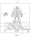
- an augmented reality scene 4 is depicted wherein a user of an AR/MR technology sees a real-world park-like setting 6 featuring people, trees, buildings in the background, and a concrete platform 8.
- the end user of the AR/MR technology also perceives that he "sees" a robot statue 10 standing upon the real-world platform 8, and a cartoon-like avatar character 12 flying by which seems to be a personification of a bumble bee, even though these elements 10, 12 do not exist in the real world.
- the human visual perception system is very complex, and producing a VR, AR, and/or MR technology that facilitates a comfortable, natural-feeling, rich presentation of virtual image elements amongst other virtual or real-world imagery elements is challenging.
- Some VR, AR, and/or MR systems employ head-worn displays (or helmet-mounted displays, or smart glasses) that are at least loosely coupled to a user's head, and thus move when the end user's head moves. If the end user's head motions are detected by the display subsystem, the data being displayed can be updated to take the change in head pose (i.e., the orientation and/or location of user's head) into account.
- Head-worn displays that enable AR/MR i.e., the concurrent viewing of real and virtual objects
- a camera captures elements of a real scene
- a computing system superimposes virtual elements onto the captured real scene
- a non-transparent display presents the composite image to the eyes.
- Another configuration is often referred to as an "optical see-through” display, in which the end user can see through transparent (or semi-transparent) elements in the display subsystem to view directly the light from real objects in the environment.
- the transparent element often referred to as a “combiner,” superimposes light from the display over the end user's view of the real world.
- Some head-worn VR/AR/MR systems employ a display screen in the field of view of the end user and an image projection assembly that projects images onto the display screen.
- the image projection assembly may take the form of an optical fiber scan-based image projection assembly
- the display screen may take the form of a optical waveguide-based display into which scanned and collimated light beams from the image projection assembly are injected via an in-coupling (IC) element, which the exit the surface of the optical waveguide-based display towards the user's eyes, thereby producing, e.g., images at single optical viewing distance closer than infinity (e.g., arm's length), images at multiple, discrete optical viewing distances or focal planes, and/or image layers stacked at multiple viewing distances or focal planes to represent volumetric 3D objects.
- IC in-coupling
- the entrance pupil of the user's eye i.e., the image of the anatomical pupil as seen through the cornea
- the exit pupil of the display screen i.e., the width of the cone of light that is available to the eye of the user
- a fixed eye relief i.e., the distance from the last surface of the display screen and the user's eye or eyes.
- An exit pupil of the display screen that is smaller than the entrance pupil of the user' eye will often result in a vignette or clipped image, whereas an exit pupil of the display screen that is larger than the entrance pupil of the user's eye wastes some light, but allows for movement of the eye without vignetting or clipping of the image.
- the exit pupil of the display screen should create an "eye box" that is slightly larger (e.g., 10mm) than the entrance pupil of the user's eye (e.g., 5-7mm) to allow movement of the eye within that eye box to maintain a full view of the image presented by the display screen.
- the visualization center of the brain gains valuable perception information from the motion of both eyes and components thereof relative to each other.
- Vergence movements i.e., rolling movements of the pupils toward or away from each other to converge the lines of sight of the eyes to fixate upon an object
- vergence movements of the two eyes relative to each other are closely associated with focusing (or "accommodation") of the lenses of the eyes.
- accommodation movements i.e., rolling movements of the pupils toward or away from each other to converge the lines of sight of the eyes to fixate upon an object
- accommodation or "accommodation-vergence reflex"
- a change in vergence will trigger a matching change in accommodation, under normal conditions.
- Working against this reflex is known to produce eye fatigue, headaches, or other forms of discomfort in users.
- One possible approach to address these problems is to project images at multiple depth planes.
- one approach is to use a plurality of light guiding optical elements to direct light at the eyes of a user such that the light appears to originate from multiple depth planes.
- the light guiding optical elements are designed to incouple virtual light corresponding to digital or virtual objects and propagate it by total internal reflection ("TIR"), then to out-couple the virtual light to display the digital or virtual objects to the user's eyes.
- TIR total internal reflection
- the light guiding optical elements are also designed to be transparent to light from (e.g., reflecting off of) actual real-world objects. Therefore, portions of the light guiding optical elements are designed to reflect virtual light for propagation via TIR while being transparent to real-world light from real-world objects.
- VR/AR/MR systems generate images at various depths for displaying VR/AR/MR scenarios. Some such optical systems are described in U.S. Utility Patent Application Serial No. 14/555,585 , the contents of which have been previously incorporated by reference.
- Some VR/AR/MR systems employ wearable display devices (e.g., head-worn displays, helmet-mounted displays, or smart glasses) that are at least loosely coupled to a user's head, and thus move when the user's head moves.
- 3-D optical systems such as those in VR/AR/MR systems, optically render virtual objects.
- Objects are "virtual" in that they are not real physical objects located in respective positions in 3-D space. Instead, virtual objects only exist in the brains (e.g., the optical centers) of viewers and/or listeners when stimulated by light beams directed to the eyes of audience members.
- VR/AR/MR systems must also be capable of displaying virtual digital content at various perceived positions and distances relative to the user.
- the design of VR/AR/MR systems presents numerous other challenges, including the speed of the system in delivering virtual digital content, quality of virtual digital content, eye relief of the user (addressing the vergence-accommodation conflict), size and portability of the system, and other system and optical challenges.
- VR/AR/MR systems must be capable of displaying virtual digital content in sharp focus to generate photo-realistic imagery required for a believable, immersive, enjoyable VR/AR/MR experience/scenario.
- the lens of an eye must change shape (i.e., accommodate) to bring images or portions thereof into better focus.
- Head-worn VR/AR/MR display systems such as those described in U.S. Utility Patent Application Serial No. 14/555,585 , the contents of which have been previously incorporated by reference, display images to users with light beams transmitted by TIR through light guiding optical elements which conserve light beam angles. Light beam diameters remain essentially the same through light guiding optical elements. Size limitations of head-worn displays limited the size of various optical components (e.g., light sources, light guiding optical elements, lenses, etc.), which limits the diameters of light beams generated by the head-worn displays. These light beam diameter limitations result in resolution and FOV limitations described above.
- a virtual image generation system comprises a planar optical waveguide (which may be a single unitary substrate) having opposing first and second faces, and an in-coupling (IC) element configured for optically coupling a collimated light beam from an image projection assembly into the planar optical waveguide as an in-coupled light beam.
- the image projection assembly may comprise a scanning device configured for scanning the collimated light beam.
- the virtual image generation system further comprises a first orthogonal pupil expansion (OPE) element associated with the first face of the planar optical waveguide for splitting the in-coupled light beam into a first set of orthogonal light beamlets, and a second orthogonal pupil expansion (OPE) element associated with the second face of the planar optical waveguide for splitting the in-coupled light beam into a second set of orthogonal light beamlets.
- OPE orthogonal pupil expansion
- OPE orthogonal pupil expansion
- second OPE element associated with the second face of the planar optical waveguide for splitting the in-coupled light beam into a second set of orthogonal light beamlets.
- the first OPE element is disposed on the first face of the planar optical waveguide
- the second OPE element is disposed on the second face of the planar optical waveguide.
- the IC element may be configured for optically coupling the collimated light beam from the image projection assembly as the in-coupled light beam for propagation within the planar optical waveguide via total internal reflection (TIR) along a first optical path that alternately intersects the first OPE element and the second OPE element, such that portions of the in-coupled light beam are deflected as the respective first set of orthogonal light beamlets and the second set of orthogonal light beamlets that propagate within the planar optical waveguide via TIR along second parallel optical paths.
- the second parallel optical paths may be orthogonal to the first optical path.
- the virtual image generation system further comprises an exit pupil expansion (EPE) element associated with the planar optical waveguide for splitting the first and second sets of orthogonal light beamlets into an array of out-coupled light beamlets (e.g., a two-dimensional out-coupled light beamlet array) that exit the planar optical waveguide.
- EPE exit pupil expansion
- the collimated light beam may define an entrance pupil
- the out-coupled light beamlet array may define an exit pupil larger than the entrance pupil, e.g., at least ten times larger than the entrance pupil, or even at least one hundred times larger than the entrance pupil.
- the EPE element is disposed on one of the first and second surfaces of the planar optical waveguide.
- the first set of orthogonal light beamlets and the second set of orthogonal light beamlets may intersect the EPE element, such that portions of the first set of orthogonal light beamlets and the second set of orthogonal light beamlets are deflected as the out-coupled light beamlet array out of the planar optical waveguide.
- the EPE element is configured for imparting a convex wavefront profile on the out-coupled light beamlet array exiting the planar optical waveguide.
- the convex wavefront profile may have a center of radius at a focal point to produce an image at a given focal plane.
- each of the IC element, OPE element, and EPE element is diffractive.
- a virtual image generation system comprises a planar optical waveguide comprising a plurality of substrates including a primary substrate having a first thickness, at least two secondary substrates having second thicknesses, and at least two semi-reflective interfaces respectively disposed between the substrates.
- each of the semi-reflective interfaces comprises a semi-reflective coating, which may be, e.g., respectively disposed between the substrates via one of physical vapor deposition (PVD), ion-assisted deposition (IAD), and ion beam sputtering (IBS).
- Each of the coatings may, e.g., be composed of one or more of a metal (Au, Al, Ag, Ni-Cr, Cr and so on), dielectric (Oxides, Fluorides and Sulfides), and semiconductors (Si, Ge).
- adjacent ones of the substrates are composed of materials having different indices of refraction.
- the virtual image generation system further comprises one or more diffractive optical elements (DOEs) associated with the planar optical waveguide for further splitting the plurality of primary light beamlets into an array of out-coupled light beamlets (e.g., a two-dimensional out-coupled beamlet array) that exit a face of the planar optical waveguide.
- DOEs diffractive optical elements
- the collimated light beam may define an entrance pupil
- the out-coupled light beamlet array may define an exit pupil larger than the entrance pupil, e.g., at least ten times larger than the entrance pupil, or even at least one hundred times larger than the entrance pupil.
- the first thickness of the primary substrate and the second thicknesses of the secondary substrates are selected, such that spacings between centers of at least two adjacent ones of the out-coupled light beamlets are equal to or less than a width of the collimated light beam. In another embodiment, the first thickness and the second thicknesses are selected, such that no gap resides between edges of greater than half of adjacent ones of the out-coupled light beamlets.
- the semi-reflective interfaces are configured for splitting the in-coupled light beam into at least two in-coupled light beamlets.
- the DOE(s) comprises an orthogonal pupil expansion (OPE) element configured for respectively splitting the at least two in-coupled light beamlets into at least two sets of orthogonal light beamlets
- the semi-reflective interfaces are further configured for splitting the at least two sets of orthogonal light beamlets into at least four sets of orthogonal light beamlets
- the DOE(s) comprises an exit pupil expansion (EPE) element configured for splitting the at least four sets of orthogonal light beamlets into the set of out-coupled light beamlets.
- the OPE element and EPE element may be disposed on a face of the optical planar waveguide.
- the EPE element may be configured for imparting a convex wavefront profile on the out-coupled light beamlet array exiting the planar optical waveguide.
- the convex wavefront profile may have a center of radius at a focal point to produce an image at a given focal plane.
- a virtual image generation system comprises a planar optical waveguide comprising a plurality of substrates including a primary substrate having a first thickness, at least one secondary substrate respectively having at least one second thicknesses, and at least one semi-reflective interface respectively disposed between the substrates.
- the first thickness is at least twice each of the at least one second thickness.
- the first thickness is a non-multiple of each of the second thickness(es).
- the secondary substrate(s) comprises a plurality of secondary substrates.
- the second thicknesses may be equal to each other or two or more of the secondary substrate(s) may have second thicknesses that are not equal to each other.
- the first thickness may be a non-multiple of at least one of the second thicknesses. At least two of the unequal second thicknesses may be non-multiples of each other.
- each of the semi-reflective interface(s) comprises a semi-reflective coating, which may be, e.g., respectively disposed between the substrates via one of physical vapor deposition (PVD), ion-assisted deposition (IAD), and ion beam sputtering (IBS).
- Each of the coatings may, e.g., be composed of one or more of a metal (Au, Al, Ag, Ni-Cr, Cr and so on), dielectric (Oxides, Fluorides and Sulfides), and semiconductors (Si, Ge).
- adjacent ones of the substrates are composed of materials having different indices of refraction.
- the second diffractive index of the second light guiding optical sub-element facilitates substantially total internal reflection of light beams substantially parallel to an optical axis of the system to a greater degree than light beams oblique to the optical axis.
- the second light guiding optical sub-element may overlay substantially all of the first light guiding optical sub-element.
- the orthogonal pupil expander includes a first orthogonal pupil sub-expander and a second orthogonal pupil sub-expander.
- Each of the first and second orthogonal pupil sub-expanders divides light beams entering the respective first and second orthogonal pupil sub-expanders.
- Each of the first and second orthogonal pupil sub-expanders may be a respective flat sheet.
- the first and second orthogonal pupil sub-expanders may be stacked on top of each other.
- the first orthogonal pupil sub-expander includes a first exit edge to direct beamlets into the second orthogonal pupil sub-expander.
- the first exit edge may include a mirror.
- the first orthogonal pupil sub-expander may include a second exit edge to direct beamlets into the second orthogonal pupil sub-expander.
- the first and second exit edges may each include a respective mirror.
- the orthogonal pupil expander includes first and second reflective edges.
- the first and second reflective edges may be orthogonal to each other.
- the orthogonal pupil expander may also include a third reflective edge.
- the orthogonal pupil expander includes an in-coupling grating and a region of high diffraction disposed opposite of the in-coupling grating.
- the orthogonal pupil expander may include a first light modifier configured to absorb light in a first wavelength range.
- the orthogonal pupil expander may also include a second light modifier configured to absorb light in a second wavelength range.
- the first and second light modifiers may be orthogonal to each other.
- the virtual image generation system 100 may be employed in applications other than augmented reality and virtual reality subsystems.
- various techniques may be applied to any projection or display subsystem, or may be applied to pico projectors where movement may be made by an end user's hand rather than the head.
- the teachings should not be limited to such subsystems of such uses.
- the virtual image generation system 100 comprises a frame structure 102 worn by an end user 50, a display subsystem 104 carried by the frame structure 102, such that the display subsystem 104 is positioned in front of the eyes 52 of the end user 50, and a speaker 106 carried by the frame structure 102, such that the speaker 106 is positioned adjacent the ear canal of the end user 50 (optionally, another speaker (not shown) is positioned adjacent the other ear canal of the end user 50 to provide for stereo/shapeable sound control).
- the display subsystem 104 is designed to present the eyes 52 of the end user 50 with photo-based radiation patterns that can be comfortably perceived as augmentations to physical reality, with high-levels of image quality and three-dimensional perception, as well as being capable of presenting two-dimensional content.
- the display subsystem 104 presents a sequence of frames at high frequency that provides the perception of a single coherent scene.
- the display subsystem 104 employs "optical see-through” display through which the user can directly view light from real objects via transparent (or semi-transparent) elements.
- the transparent element often referred to as a “combiner,” superimposes light from the display over the user's view of the real world.
- the display subsystem 104 comprises a projection subsystem 108 and a partially transparent display screen 110 on which the projection subsystem 108 projects images.
- the display screen 110 is positioned in the end user's 50 field of view between the eyes 52 of the end user 50 and an ambient environment, such that direct light from the ambient environment is transmitted through the display screen 110 to the eyes 52 of the end user 50.
- the image projection assembly 108 provides a scanned light to the partially transparent display screen 110, thereby combining with the direct light from the ambient environment, and being transmitted from the display screen 110 to the eyes 52 of the user 50.
- the projection subsystem 108 takes the form of an optical fiber scan-based projection device
- the display screen 110 takes the form of a waveguide-based display into which the scanned light from the projection subsystem 108 is injected to produce, e.g., images at a single optical viewing distance closer than infinity (e.g., arm's length), images at multiple, discrete optical viewing distances or focal planes, and/or image layers stacked at multiple viewing distances or focal planes to represent volumetric 3D objects.
- the virtual image generation system 100 further comprises one or more sensors (not shown) mounted to the frame structure 102 for detecting the position and movement of the head 54 of the end user 50 and/or the eye position and interocular distance of the end user 50.
- sensors may include image capture devices (such as cameras), microphones, inertial measurement units, accelerometers, compasses, GPS units, radio devices, and/or gyros).
- the virtual image generation system 100 further comprises a user orientation detection module 112.
- the user orientation module 112 detects the instantaneous position of the head 54 of the end user 50 and may predict the position of the head 54 of the end user 50 based on position data received from the sensor(s). Detecting the instantaneous position of the head 54 of the end user 50 facilitates determination of the specific actual object that the end user 50 is looking at, thereby providing an indication of the specific textual message to be generated for that actual object and further providing an indication of the textual region in which the textual message is to be streamed.
- the user orientation module 112 also tracks the eyes 52 of the end user 50 based on the tracking data received from the sensor(s).
- the virtual image generation system 100 further comprises a control subsystem that may take any of a large variety of forms.
- the control subsystem includes a number of controllers, for instance one or more microcontrollers, microprocessors or central processing units (CPUs), digital signal processors, graphics processing units (GPUs), other integrated circuit controllers, such as application specific integrated circuits (ASICs), programmable gate arrays (PGAs), for instance field PGAs (FPGAs), and/or programmable logic controllers (PLUs).
- controllers for instance one or more microcontrollers, microprocessors or central processing units (CPUs), digital signal processors, graphics processing units (GPUs), other integrated circuit controllers, such as application specific integrated circuits (ASICs), programmable gate arrays (PGAs), for instance field PGAs (FPGAs), and/or programmable logic controllers (PLUs).
- the control subsystem of virtual image generation system 100 comprises a central processing unit (CPU) 114, a graphics processing unit (GPU) 116, one or more frame buffers 118, and three-dimensional data base 120 for storing three-dimensional scene data.
- the CPU 114 controls overall operation, while the GPU 116 renders frames (i.e., translating a three-dimensional scene into a two-dimensional image) from the three-dimensional data stored in the three-dimensional data base 120 and stores these frames in the frame buffer(s) 116.
- one or more additional integrated circuits may control the reading into and/or reading out of frames from the frame buffer(s) 116 and operation of the image projection assembly 108 of the display subsystem 104.
- the various processing components of the virtual image generation system 100 may be physically contained in a distributed subsystem.
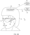
- the virtual image generation system 100 comprises a local processing and data module 130 operatively coupled, such as by a wired lead or wireless connectivity 136, to the display subsystem 104 and sensors.
- the local processing and data module 130 may be mounted in a variety of configurations, such as fixedly attached to the frame structure 102 ( Fig. 3A ), fixedly attached to a helmet or hat 56 ( Fig. 3B ), embedded in headphones, removably attached to the torso 58 of the end user 50 ( Fig.
- the virtual image generation system 100 further comprises a remote processing module 132 and remote data repository 134 operatively coupled, such as by a wired lead or wireless connectivity 138, 140, to the local processing and data module 130, such that these remote modules 132, 134 are operatively coupled to each other and available as resources to the local processing and data module 130.
- the local processing and data module 130 may comprise a power-efficient processor or controller, as well as digital memory, such as flash memory, both of which may be utilized to assist in the processing, caching, and storage of data captured from the sensors and/or acquired and/or processed using the remote processing module 132 and/or remote data repository 134, possibly for passage to the display subsystem 104 after such processing or retrieval.
- the remote processing module 132 may comprise one or more relatively powerful processors or controllers configured to analyze and process data and/or image information.
- the remote data repository 134 may comprise a relatively large-scale digital data storage facility, which may be available through the internet or other networking configuration in a "cloud" resource configuration. In some embodiments, all data is stored and all computation is performed in the local processing and data module 130, allowing fully autonomous use from any remote modules.
- the couplings 136, 138, 140 between the various components described above may include one or more wired interfaces or ports for providing wires or optical communications, or one or more wireless interfaces or ports, such as via RF, microwave, and IR for providing wireless communications.
- all communications may be wired, while in other implementations all communications may be wireless.
- the choice of wired and wireless communications may be different from that illustrated in Figs. 3A-3D . Thus, the particular choice of wired or wireless communications should not be considered limiting.
- a diffraction pattern, or diffractive optical element may be embedded within or imprinted/embossed upon a light guiding optical element (“LOE”; e.g., a planar waveguide) such that as collimated light (light beams with substantially planar wavefronts) is substantially totally internally reflected along the LOE, it intersects the diffraction pattern at multiple locations and exits toward the user's eye.
- LOE light guiding optical element
- the DOEs are configured so that light exiting therethrough from an LOE are verged so that they appear to originate from a particular depth plane.
- the collimated light may be generated using an optical condensing lens (a "condenser").
- a first LOE may be configured to deliver collimated light to the eye that appears to originate from the optical infinity depth plane (0 diopters).
- Another LOE may be configured to deliver collimated light that appears to originate from a distance of 2 meters (1/2 diopter).
- Yet another LOE may be configured to deliver collimated light that appears to originate from a distance of 1 meter (1 diopter).
- a stacked LOE assembly it can be appreciated that multiple depth planes may be created, with each LOE configured to display images that appear to originate from a particular depth plane. It should be appreciated that the stack may include any number of LOEs. However, at least N stacked LOEs are required to generate N depth planes. Further, N, 2N or 3N stacked LOEs may be used to generate RGB colored images at N depth planes.
- the mixed reality (MR) system projects images of the virtual content into the user's eye so that they appear to originate from various depth planes in the Z direction (i.e., orthogonally away from the user's eye).
- the virtual content may not only change in the X and Y directions (i.e., in a 2D plane orthogonal to a central visual axis of the user's eye), but it may also appear to change in the Z direction such that the user may perceive an object to be very close or at an infinite distance or any distance in between.
- the user may perceive multiple objects simultaneously at different depth planes. For example, the user may see a virtual dragon appear from infinity and run towards the user. Alternatively, the user may simultaneously see a virtual bird at a distance of 3 meters away from the user and a virtual coffee cup at arm's length (about 1 meter) from the user.
- Multiple-plane focus systems create a perception of variable depth by projecting images on some or all of a plurality of depth planes located at respective fixed distances in the Z direction from the user's eye.
- multiple-plane focus systems may display frames at fixed depth planes 502 (e.g., the six depth planes 502 shown in Fig. 9 ).
- MR systems can include any number of depth planes 502
- one exemplary multiple-plane focus system has six fixed depth planes 502 in the Z direction.
- 3-D perception is created such that the user perceives one or more virtual objects at varying distances from the user's eye.
- depth planes 502 are generated closer to the eye, as shown in Fig. 9 .
- the depth planes 502 may be placed at equal distances away from each other.
- the AR system may work as a multiple-plane focus system.
- all six LOEs may be illuminated simultaneously, such that images appearing to originate from six fixed depth planes are generated in rapid succession with the light sources rapidly conveying image information to LOE 1, then LOE 2, then LOE 3 and so on.
- a portion of the desired image, comprising an image of the sky at optical infinity may be injected at time 1 and the LOE 1090 retaining collimation of light (e.g., depth plane 6 from Fig. 9 ) may be utilized.
- an image of a closer tree branch may be injected at time 2 and an LOE 1090 configured to create an image appearing to originate from a depth plane 10 meters away (e.g., depth plane 5 from Fig.
- AR systems are required to project images (i.e., by diverging or converging light beams) that appear to originate from various locations along the Z axis (i.e., depth planes) to generate images for a 3-D experience/scenario.
- light beams include, but are not limited to, directional projections of light energy (including visible and invisible light energy) radiating from a light source.
- Generating images that appear to originate from various depth planes conforms the vergence and accommodation of the user's eye for that image, and minimizes or eliminates vergence-accommodation conflict.
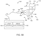
- the drive assembly 156 comprises a piezoelectric element 160 to which the optical fiber(s) 154 is mounted, and drive electronics 162 configured for conveying electrical signals to the piezoelectric element 160, thereby causing the distal end 154b of the optical fiber 154 to vibrate in accordance with the scan pattern.
- operation of the light source(s) 150 and drive electronics 162 are coordinated in a manner that generates image data that is encoded in the form of light that is spatially and/or temporally varying.
- Descriptions of optical fiber scanning techniques are provided in U.S. Patent No. 2015/0309264 , which is expressly incorporated herein by reference.
- the OCG 1498 is configured to allow a portion of a light beam to exit the beam multiplier 1430 while another portion of the light beam propagates along the beam multiplier 1430 via substantially TIR.
- the OCG 1498 may be a diffractive optical element of any type, including volumetric or surface relief.
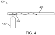
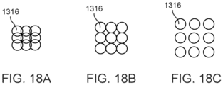
- the beam multiplier 1430 clones a single input beam 1410 into three output beamlets 1416, which each encode the same pixel information as the input beam 1410.
- the beam multiplier 1430 may have a length and a width like the OPE 494 and/or the EPE 496 shown in Fig. 67 . Further, while the input beams 1410 are depicted as propagating in a generally left to right direction, the beam multiplier 1430 may be configured to direct light beams in a variety of patterns, including but not limited to zigzag patterns that generate an array of beamlets 1416 (see e.g., Fig. 18B ).
- Fig. 20 shows that only some (i.e., one) of the beamlets 1516 exiting from the beam multiplier 1530 pass through the pupil 1506 defined by the iris 1508 to be focused by the lens 1502. Therefore, even with beam multiplication, spacing of beamlets 1516 can affect the actual number of beams perceived by a user.
- Fig. 20 also shows that the number of bounces of the input beams 1510 per length of the beam multiplier 1530 determines the number of beamlets 1516 exiting from a given length the beam multiplier 1530.
- Fig. 21 depicts a thinner beam multiplier 1630' according to some embodiments.
- a thicker beam multiplier 1630 is also depicted for comparison.
- each input light beam 1610 (which angle of incidence preserve between the two the multipliers) bounces more times in the thinner beam multiplier 1630' compared to the thicker beam multiplier 1630.
- the input light beam 1610 bounces back and forth a higher spatial frequency because there is less distance to traverse before the beam 1610 encounters each surface of the thinner beam multiplier 1630'. Accordingly, a higher density of beamlets emerge from the thinner beam multiplier 1630' compared to the thicker beam multiplier 1630.
- the beam multipliers depicted in Figs. 19-21 include two opposing reflective surfaces that reflect light in substantially opposite directions to enable substantially TIR. In other embodiments, beam multipliers include more than two reflective surfaces.
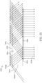
- the multi-surface beam multiplier 1730 depicted in Fig. 22A includes first and second light guiding optical sub-elements ("LOS") 1730A, 1730B.
- the first LOS 1730A is similar to the beam multiplier 1530 depicted in Fig. 20 in that it has two (i.e., first and second) opposing reflective surfaces 1732, 1734.
- the second LOS 1730B depicted in Fig. 22A has a third reflective surface 1736 that reflects light in substantially the same direction as the second reflective surface 1734 in the first LOS 1730A.
- the second LOS 1730B is disposed over the first LOS 1730A such that an incoming light beam 1710 at least partially passes through the first LOS 1730A and enters the second LOS 1730B.
- a portion thereof is partially reflected by the second reflective surface 1734.
- the portion of the incoming light beams 1710 that passes through the second LOS 1730B is reflected by the third reflective surface 1736 in substantially the same direction as the portion of the incoming light beam 1710 that is reflected by the second reflective surface 1734.
- the result of the addition of the second LOS 1730B and its third reflective surface 1736 is a multiplication of the number of beamlets 1716 propagating along the first and second LOSs 1730A, 1730B by substantially TIR.
- the thickness of the second LOS 1730B depicted in Fig. 22A is such that some of beamlets 1716 reflecting off of the third reflective surface 1736 substantially overlap with the beamlets 1716 reflecting off of the second reflective surface 1734.
- some of the beamlets 1716 are out of phase with one another, such overlap can serve to amplify the effects of destructive interference between phase-mismatched beamlets.
- high levels of overlap can serve to minimize the degree of multiplication of the number of beamlets 1716. For instance, while the first bounce off of the second and third reflective surfaces 1734, 1736 multiplies the number of beams 1710/beamlets 1716 from 1 to 2, the second bounce only multiplies the number of beamlets 1716 from 2 to 3.
- the extent to which at least some of beamlets 1716 overlap can be controlled by adjusting the input beam 1710 diameter and/or the input beam 1710 separation, both of which are substantially conserved during substantially TIR.
- the distance between the edges of two adjacent beamlets, from among the number of beamlets 1716, may be increased by reducing the diameter of the input beam 1710.
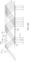
- the beam multiplier 1730 depicted in Fig. 22B includes first and second LOSs 1730A, 1730B, like the beam multiplier 1730 depicted in Fig. 22A .
- the thickness of the second LOS 1730B has been tuned/selected such that the beamlets 1716 reflecting off of the third reflective surface 1736 do not overlap with the beamlets 1716 reflecting off of the second reflective surface 1734. Consequently, the beam multiplier 1730 depicted in Fig. 22B has a higher degree of beamlet multiplication than the beam multiplier 1730 depicted in Fig. 22A .
- each bounce off of the second and third reflective surfaces 1734, 1736 doubles the number of beamlets 1716 in substantially exponential growth.
- the beam multiplier 1830 depicted in Fig. 23 includes first and second LOSs 1830A, 1830B, like the beam multiplier 1730 depicted in Fig. 22A .
- a difference between the beam multipliers 1730, 1830 is that the second LOS 1830B depicted in Fig. 23 has a fourth reflective surface 1838 in addition to the third reflective surface 1836.
- the third and fourth reflective surfaces 1836, 1838 are disposed on opposing sides of the second LOS 1830B, and reflect light in substantially opposite directions.
- the second LOS 1830B is disposed over the first LOS 1830A such that an incoming light beam 1810 at least partially passes through the first LOS 1830A and enters the second LOS 1830B.
- a portion thereof is partially reflected by the second reflective surface 1834.
- the portion of the incoming light beams 1810 that passes through the second LOS 1830B is reflected by the third reflective surface 1836 in substantially the same direction as the portion of the incoming light beam 1810 that is reflected by the second reflective surface 1834.
- the fourth reflective surface 1838 is reflected by the fourth reflective surface 1838 back toward the third reflective surface 1836.
- the result of the addition of the fourth reflective surfaces 1838 in the second LOS 1830B is a further multiplication of the number of beamlets 1816 propagating along the first and second LOSs 1830A, 1830B by substantially TIR even compared to the beam multiplier 1730 depicted in Fig. 22A .
- the addition of the fourth reflective surface 1838 results in an additional bounce for each light beam 1810/beamlet 1816, thereby multiplying the number of beamlets produced at each interaction with the first and second LOSs 1830A, 1830B (i.e., the light multiplier 1830).
- the beam multiplier 1930 depicted in Fig. 24 includes first and second LOSs 1930A, 1930B, like the beam multiplier 1830 depicted in Fig. 23 .
- a difference between the beam multipliers 1830, 1930 is that the beam multiplier 1930 depicted in Fig. 24 includes a third LOS 1930C.
- the third LOS 1930C includes a b of opposing reflective surfaces (i.e., fifth and sixth reflective surfaces 1940, 1942) that reflect light in substantially opposite directions.
- the fifth and sixth reflective surfaces 1940, 1942 are disposed on opposing sides of the third LOS 1930C.
- the third LOS 1930C is disposed over the second LOS 1930B (and therefore the first LOS 1930A) such that an incoming light beam 1910 at least partially passes through the first and second LOSs 1930A, 1930B and enters the third LOS 1930C.
- a portion thereof is partially reflected by the second reflective surface 1934.
- a portion thereof is partially reflected by the third reflective surface 1936.
- the portion of the incoming light beams 1910 that passes through the second LOS 1930B is reflected by the third reflective surface 1936 in substantially the same direction as the portion of the incoming light beam 1910 that is reflected by the second reflective surface 1934.
- the portion of the incoming light beams 1910 that passes through the third LOS 1930C is reflected by the fifth reflective surface 1940 in substantially the same direction as the portions of the incoming light beam 1910 that are respectively reflected by the second and third reflective surfaces 1934, 1936.
- the reflected beamlet 1916 Before the reflected beamlet 1916 exits the second LOS 1930B, a portion of the reflected beamlet 1916 is reflected by the fourth reflective surface 1938 back toward the third reflective surface 1936. Similarly, before the reflected beamlet 1916 exits the third LOS 1930C, a portion of the reflected beamlet 1916 is reflected by the sixth reflective surface 1942 back toward the fifth reflective surface 1940.
- the result of the addition of the third LOS 1930C and its fifth and sixth reflective surfaces 1940, 1942 is a further multiplication of the number of beamlets 1916 propagating along the first, second, and third LOSs 1930A, 1930B, 1930C by substantially TIR. As shown in Fig.
- the addition of the third LOS 1930C results in an additional pair of bounces for each light beam 1910/beamlet 1916, thereby multiplying the number of beamlets produced at each interaction with the first, second, and third LOSs 1930A, 1930B, 1930C (i.e., the light multiplier 1930).
- Multi-surface beam multipliers can be fabricated using a lamination process.
- a second substrate e.g., a second LOS
- a first substrate e.g., a first LOS
- the interface between the two substrates may be partially reflective (e.g., a metallic coating/half-silvered mirror, a thin film coating, a dichroic mirror, a dielectric interface, a diffraction grating, a diffractive element, etc.)
- separate waveguides/LOEs can be laminated together with a partially-reflective interface.
- the ratio of thicknesses of first and second LOSs can affect beamlet multiplication by beamlet overlap. If the respective thicknesses are whole number multiples or quotients (i.e., factors), then cloned beamlets may overlap when they exit the first and second LOSs, reducing the degree of beamlet multiplication. Therefore, in some embodiments (see Fig. 22B ) the first thickness of the first LOS may be a non-even factor of the second thickness of the second LOS. For instance, the first thickness may be 0.3256 times the second thickness (instead of e.g., 0.2 or 0.5). Quasi-random beamlet arrays with multiple LOSs may be insensitive to angle or imperfections in LOS thicknesses.
- Beam multipliers can also be tuned by varying the degree of reflectiveness/transmittance of various surfaces (e.g., other than 50/50). Using this and other techniques, the multipliers can be tuned to have an even distribution of energy across the beamlets. For moderate amounts of beam multiplication (e.g., sufficient to fill the pupils of the eyes), the beam multiplier(s) can be two to ensure that beamlets (and groups thereof) have the same amounts of energy, as the eye sweeps across different sets of beamlets. Equalizing the amount of energy across beamlets minimizes dropouts in intensity (artifacts; winking) as the user's eyes sweep the FOV. With an exponentially increasing number of beamlets, beamlets will eventually randomly overlap, thereby reducing intensity artifacts.
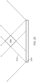
- Fig. 25 depicts a beam multiplier 2030 that is tuned/optimized to produce the most light (e.g., with an optimal beam diameter/energy distribution) for beamlets 2016 that are directed toward the center 2044 of an FOV.
- the beam multiplier 2030 can be tuned to vary the light intensity/energy as a function of the angle of the beamlets 2016 that will be emerging from the beam multiplier 2030. Beamlets 2016 directed toward the center 2044 of an FOV 10 to be more perpendicular/orthogonal to the surface of the beam multiplier 2030 (i.e., have a smaller angle of incidence).
- This design minimizes artifacts at the center 2044 of the FOV where some users' eyes will be directed most of the time, while at the same time controlling the amount of energy required to display an image.
- the beam multiplier 2030 has been less tuned/optimized for more eccentric beamlets 2016 at the peripheral portions of the FOV.
- a FOV may be expanded with kaleidoscopically tuned beam multipliers.
- the relative reflectivity of surfaces can be tuned such that the beam multiplier has dense beam multiplication in optically important regions (e.g., center of an FOV) and sparse beam multiplication in optically less important regions (e.g., periphery of an FOV).
- the FOV can be determined to various types of eye tracking, including but not limited to interpupillary distance measurement and pupil motion tracking.
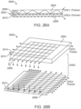
- OPE1 2604 and OPE2 2608 By varying the thicknesses of OPE1 2604 and OPE2 2608, different periodic relationships can be achieved for OPE1 2604 and OPE2 2608. This can be tuned to generate different spatial frequency for beamlet cloning. While the varied optical (light modifying) characteristic described above is LOE thickness, other optical characteristics (such as diffractive index) can also be varied to achieve effects similar to those described herein.
- exit edges 2612, 2614 There are two exit edges 2612, 2614 for OPE1 2604 (see Fig. 26B ). In some embodiments, both exits edges are coupled to OPE2 2608. In another embodiment, the diffraction efficiency of OPE1 2604 can be varied in various portions of OPE1 2604 to guide the majority of the light to one exit edge (e.g., 2606), which is coupled into OPE2 2608.
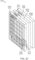
- Fig. 27 depicts a beam multiplier 2700 wherein a single OPE 2702 feeds light/optical information to 2 EPE layers 2704, 2706 using 2 spatially displaced OCGs 2708, 2710.
- OCG1 2708 couples the OPE 2702 to EPE1 2704 through ICG1 2712.
- OCG2 2710 couples the OPE 2702 to EPE2 2706 through ICG2 2714.
- the OCGs 2708, 2710 can be PDLC, which can be turned on or off.
- an LC shutter layer (not shown) can be interposed between the OPE 2702 and the EPE layers 2704, 2706.
- the number of EPE layers can be set to correspond to the number of multiple depth layers for an MR system.
- a single OCG can be divided into multiple windows with shutters or switches to selectively feed light/optical information to a plurality of EPE layers.
- the OCGs 2808, 2810 can be formed at or from two exit edges of the OPE 2802.
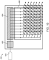
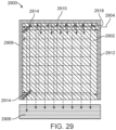
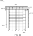
- Fig. 29 depicts a beam multiplier 2900 with an OPE 2902 designed similar to a "hall of mirrors".
- an input/primary beam 2904 is multiplied by the OPE 2902 and multiplied beamlets exit the OPE 2902 via one or more OCGs 2906.
- Three of the four OPE edges 2908, 2910, 2912 may be polished and coated with aluminum to render them reflective.
- Two opposing mirrors 2908, 2912 reflect the beams and beamlets propagating through the OPE 2902, generating additional beamlets (with the same optical information) as the reflected beamlets interact with the OPE 2902.
- Such an OPE 2902 can be tuned to have a low diffraction efficiency toward the OCG 2906, but beam multiplication will be greatly increased with multiple passes through the OPE 2902.
- the OPE 2902 may have one or more regions of relatively higher diffraction efficiency 2914 to facilitate beam multiplication by increasing the beam length through the OPE 2902 before beams/beamlets exit through the OCG 2906.
- a similar embodiment 3000 depicted in Fig. 30 only two of the edges 3010, 3012 (perpendicular edges) and a small portion of a third edge 3008 of the OPE 3002 are polished and coated with aluminum to render them reflective. This treatment results in reduced beamlet multiplication, but doubles the amount of area for exits 3016 (e.g., for OCGs (not shown)). This design increases the surface area 3016 for out-coupling.
- the OPE 2902, 3002 can be optimized/tuned with variable diffraction efficiency.
- the upper left of regions in both of these embodiments can be tuned to diffract light in an up-and-down direction and to minimize light reflected back toward the ICG 2918, 3018, which may unintentionally couple out of the OPE 2902, 3002.
- the beam multiplier 3100 depicted in Fig. 31 includes an OPE 3102 that is shared across wavelengths.
- a first OCG 3104 is tuned to out-couple green light with a blue and red light absorber 3106 coupled to the OCG 3104.
- a second OCG 3108 is tuned to out-couple blue and red (i.e., magenta) light with a green light absorber 3110 coupled to the OCG 3108.
- the beam multiplier 3200 depicted in Fig. 32 includes an OPE 3202 with three output regions 3204, 3206, 3208.
- the three output regions 3204, 3206, 3208 are tuned to respectively out-couple red 3204, green 3206, and blue 3208 light using OCGs 3204, 3206, 3208 with matching absorbers 3210, 3212, 3214.
- the DOEs 3216 in the OPE 3202 form a "V" shape 3218 with an approximately 90 degree angle, but the DOEs may form other shapes with different angles in other embodiments (e.g., to modify beamlet density (not shown)).
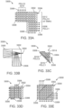
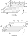
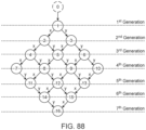
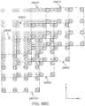
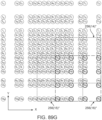
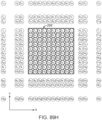
- Figs. 33A-33I illustrate various "quilts" of different OPE 3302 regions that allow tuning of OPEs 3302 for various out-coupling patterns.
- a single input/primary beam 3304 is multiplied, diffracted, and/or reflected by various components of the OPEs 3302 to form various multiplied beams/beamlets 3306 having a variety of out-coupling patterns.
- Fig. 33A depicts an OPE 3302 including three sections 3308, 3310, 3312 having different diffractive properties. The three sections may be independently switchable PDLC components (e.g., to change the out-coupling pattern) or they may be static components.
- the waveguide 172 is a single unitary substrate or plane of an optically transparent material, such as, e.g., glass, fused silica, acrylic, or polycarbonate, although in alternative embodiments, the waveguide 172 may be composed of separate distinct substrates or panes of optically transparent material that are bonded together in the same plane or in different planes.
- an optically transparent material such as, e.g., glass, fused silica, acrylic, or polycarbonate
- the IC element 168 may be closely associated with (e.g., embedded in) the face 180b of the waveguide 172 for receiving the collimated light beam 250 from the image projection assembly 108 into the waveguide 172 via the face 180b, although in alternative embodiments, the IC element 168 may be associated with (e.g., embedded in) the other face 180a or even the edge of the waveguide 172 for coupling the collimated light beam 250 into the waveguide 172 as an in-coupled light beam.
- the DOE(s) 174 are associated with the waveguide 172 (e.g., incorporated within the waveguide 172 or abutting or adjacent one or more of the faces 180a, 180b of the waveguide 172) for, as briefly discussed above, two-dimensionally expanding the effective entrance pupil of the collimated light beam 250.
- the DOE(s) 174 comprises an orthogonal pupil expansion (OPE) element 186 closely associated with (e.g., embedded in) the face 180b of the waveguide 172 for splitting the in-coupled light beam 252 into orthogonal light beamlets 254, and an exit pupil expansion (EPE) element 188 closely associated with (e.g., embedded in) the face 180b of the waveguide 172 for splitting the orthogonal light beamlets 254 into a set of out-coupled light beamlets 256 that exit the face 180b of the waveguide 172 towards the eye(s) 52 of the end user 50.
- OPE element(s) 174 and EPE element 188 may be incorporated into different panes of the waveguide 172.
- the OPE element 186 relays light along a first axis (horizontal or x-axis in Fig. 34 ), and expands the effective pupil of light along a second axis (vertical or y-axis in Fig. 34 ).
- the IC element 168 optically in-couples the collimated light beam 250 for propagation as an in-coupled light beam within the waveguide 172 via TIR along an internally reflective optical path parallel to an axis 262 (in this case, along the vertical or y-axis), and in doing so, repeatedly intersects the OPE element 186.
- the OPE element 186 has a relatively low diffraction efficiency (e.g., less than 50%), and comprises a series of diagonal diffractive elements (forty-five degrees relative to the x-axis), such that, at each point of intersection with the OPE element 186, a portion (e.g., greater than 90%) of the in-coupled light beam 252 continues to propagate within the waveguide 172 via TIR along an internally reflective optical path parallel to the axis 262 (y-axis), and the remaining portion (e.g., less than 10%) of the in-coupled light beam 252 is diffracted as an orthogonal light beamlet 254 (shown as being dashed in Fig.
- a portion e.g., greater than 90%
- the remaining portion e.g., less than 10%
- axis 264 that propagates within the waveguide 172 via TIR along an internally reflective optical path parallel to the axis 264 (in this case, along the horizontal or x-axis) toward the EPE element 188.
- the axis 264 may alternatively be obliquely oriented with respect to axis 262 (y-axis).
- each orthogonal light beamlet 254 continues to propagate in the waveguide 172 via TIR along the respective internally reflective optical path parallel to the axis 264 (x-axis), and the remaining portion (e.g., less than 10%) of the respective orthogonal light beamlet 254 is diffracted as secondary light beamlets 256 that propagate within the waveguide 172 via TIR along respective internally reflective optical paths (shown by dashed lines) parallel to the axis 262 (y-axis).
- each secondary light beamlet 256 continues to propagate in the waveguide 172 via TIR along a respective internally reflective optical path parallel to the axis 262 (y-axis), and the remaining portion (e.g., less than 10%) of the respective secondary light beamlet 256 is diffracted as tertiary light beamlets 258 that combine in phase with the orthogonal light beamlets 254 and propagate within the waveguide 172 via TIR along respective internally reflective optical paths parallel to the axis 264 (x-axis).
- the entrance pupil of the collimated light beam 250 in-coupled into the display screen 110 is expanded vertically along the y-axis by the OPE element 186.
- the EPE element 188 further expands the light's effective exit pupil along the first axis (horizontal x-axis in Fig. 36 ).
- the EPE element 188 like the OPE element 186, has a relatively low diffraction efficiency (e.g., less than 50%), such that, at each point of intersection with the EPE element 188, a portion (e.g., greater than 90%) of each orthogonal light beamlet 254 continues to propagate within the waveguide 172 respectively along an respective internally reflective optical path parallel to the axis 264 (x-axis), and the remaining portion of each orthogonal light beamlet 254 is diffracted as an out-coupled light beamlet 256 that exits the face 180b of the waveguide 172 (along the z-axis), as illustrated in Fig.
- a relatively low diffraction efficiency e.g., less than 50%
- each orthogonal light beamlet 254 into multiple out-coupled light beamlets 256
- the entrance pupil of the collimated light beam 250 is further expanded horizontally along the x-axis by the EPE element 188, resulting in a two-dimensional array of out-coupled light beamlets 256 that resemble a larger version of the original in-coupled light beam 252.
- the OPE element 186 and EPE element 188 are illustrated in Fig. 34 as non-overlapping in the x-y plane, the OPE element 186 and EPE element 188 may overlap each other in the x-y plane, as illustrated in Fig. 39 , or may partially overlap each other in the x-y plane, as illustrated in Fig. 38 . In both cases, like in the embodiment illustrated in Fig.
- the OPE element 186 will split the in-coupled light beam 252 that propagates within the waveguide 172 via TIR along an internally reflective optical path parallel to the axis 262 (y-axis) into orthogonal light beamlets 254 that propagate within the waveguide 172 via TIR along respective internally reflective optical paths parallel to the axis 264 (x-axis).
- the OPE element 186 and EPE element 188 will need to be respectively disposed on opposite faces 180a, 180b of the waveguide 172.
- the EPE element 188 serves to focus the output set of light beamlets 256 at along a given focal plane, such that a portion of an image or virtual object is seen by end user 50 at a viewing distance matching that focal plane.
- the out-coupled light beamlets 256 exiting the face 180b of the waveguide 172 toward the eye(s) 52 of the end user 50 will be substantially parallel, as shown in Fig. 39A , which would be interpreted by the brain of the end user 50 as light from a viewing distance (focal plane) at optical infinity.
- the out-coupled light beamlets 256 exiting the face 180b of the waveguide 172 will be rendered more divergent from the perspective of the eye(s) 52 of the end user 50 (i.e., a convex curvature will be imparted on the light wavefront), and require the eye(s) 52 to accommodate to a closer distance to bring the resulting image into focus on the retina and would be interpreted by the brain of the end user 50 as light from a viewing distance (e.g., four meters) closer to the eye(s) 52 than optical infinity, as shown in Fig. 39B .
- a viewing distance e.g., four meters
- the out-coupled light beamlets 256 exiting the face 180b of the waveguide 172 can be rendered even more divergent from the perspective of the eye(s) 52 of the end user 50 (i.e., a more convex curvature will be imparted on the light wavefront), and require the eye(s) 52 to accommodate to an even closer distance to bring the resulting image into focus on the retina and would be interpreted by the brain of the end user 50 as light from a viewing distance (e.g., 0.5 meters) closer to the eye(s) 52, as shown in Fig. 39C .
- a viewing distance e.g., 0.5 meters
- waveguide apparatus 170 has been described herein as having only one focal plane, it should be appreciated that multiple planar optical waveguides 172 with associated OPEs 176 and EPEs 178 can be used to simultaneously or sequentially generate images at multiple focal planes, as discussed in U.S. Patent Publication Nos. 2015/0309264 and 2015/0346490 , which are expressly incorporated herein by reference.
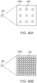
- the exit pupil of the display screen 110 may not be optimally saturated.
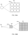
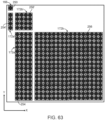
- the pupil of the collimated light beam 250 may be expanded to an exit pupil 300a of a 3 x 3 array of out-coupled light beamlets 256, which are relatively sparse in nature (i.e., the gaps between the out-coupled light beamlets 256 are relatively large).
- the display screen 110 may be enhanced with beam-multiplication features, such that the pupil of the collimated light beam 250 is expanded to an exit pupil 300b of a more saturated 9 x 9 array of out-coupled light beamlets 256, as illustrated in Fig. 40B .
- two OPEs 186 are employed to double the number of orthogonal light beamlets 254 obtained from the in-coupled light beam 252, and thus, double the saturation of the two-dimensional array of out-coupled light beamlets 256 that exit the face 180b of the waveguide 172.
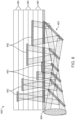
- a waveguide apparatus 170a is similar to the waveguide apparatus 170 described, with the exception that the waveguide apparatus 170a comprises a first OPE element 186a disposed adjacent (e.g., on) the first face 180a of the waveguide 172 for splitting the in-coupled light beam 252 propagating within the waveguide 172 via TIR along an internally reflecting optical path parallel to the axis 262 (y-axis) into a first set of orthogonal light beamlets 254a for propagation within the waveguide 172 via TIR along respective internally reflecting optical paths parallel to the axis 264 (x-axis) (best shown in Fig.
- a second OPE element 186b disposed adjacent (e.g., on) the second face 180b of the waveguide 172, for splitting the in-coupled light beam 252 propagating within the waveguide 172 via TIR along an internally reflecting optical path parallel to the axis 262 (y-axis) into a second set of orthogonal light beamlets 254b for propagation within the waveguide 172 via TIR along respective internally reflecting optical paths parallel to the axis 264 (x-axis).
- the first and second sets of orthogonal light beamlets 254a, 254b alternate with each other.
- the beamlets 254a, 254b are also respectively generated from the beamlets 254a, 254b, which further creates tertiary light beamlets 258a, 258b (shown only in Fig. 41 ) that respectively combine in phase with the orthogonal light beamlets 254a, 254b.
- the first and second primary sets of light beamlets 254a, 254b intersect the EPE element 188 on the face 180b of the waveguide 172, portions of which are respectively diffracted as a first set of out-coupled light beamlets 256a and a second set of out-coupled light beamlets 256b that exit the face 180b of the waveguide 172.
- the doubling of the orthogonal light beamlets 254 correspondingly increases the saturation of the exit pupil 300a expanded by the display screen 110 (shown in Fig. 40B ).
- partially reflective interfaces are incorporated into the waveguide 172 to increase the number of light beamlets propagating within the waveguide 172, and thus, increase the saturation of the two-dimensional array of out-coupled light beamlets 256 exiting the face 180b of the waveguide 172.
- the waveguide 172 comprises a plurality of layered substrates having at least one pair of adjacent substrates and a semi-reflective interface between each of the pair(s) of adjacent substrates, such that a light beam that intersects each semi-reflective interface is split into multiple beamlets that propagate within the waveguide 172 via TIR, thereby increasing the density of the out-coupled light beamlets exiting the face 180b of the waveguide 172.
- adjacent substrates described below are not drawn to scale and are illustrated as being multiples of each other for purposes of simplicity. However, adjacent substrates may be, and preferably are, non-multiples of each other, such that the density of the in-fill of out-coupled light beamlets exiting the face of the waveguide is maximized.
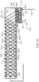
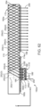
- a waveguide apparatus 170b is similar to the waveguide apparatus 170 described, with the exception that the waveguide 172 is a composite substrate composed of a primary waveguide 172a and secondary waveguide 172b.
- the waveguide apparatus 170b further comprise a semi-reflective interface 190 disposed between the primary waveguide 172a and secondary waveguide 172b.
- the ratio of reflection to transmission of the semi-reflective coating 190 may be selected or determined based at least in part upon the thickness of the coating 190, or the semi-reflective coating 190 may have a plurality of small perforations to control the ratio of reflection to transmission.
- the primary waveguide 172a and secondary waveguide 172b are composed of materials having different indices of refraction, such that the interface between the waveguides 172a, 172b are semi-reflective for light that is incident on the semi-reflective interface of less than a critical angle (i.e., the incidence angle at which a portion of the light is transmitted through the semi-reflective interface, and the remaining portion of the light is reflected by the semi-reflective interface).
- the semi-reflective interface 190 is preferably designed, such that the angle of a light beam incident on the semi-reflective interface 190 is preserved.
- the IC element 168 couples the collimated light beam 250 into the planar optical waveguide 172 as an in-coupled light beam 252, which propagates within the waveguide 172 via TIR along an internally reflective optical path parallel to the axis 262 (y-axis).
- the semi-reflective interface 190 is configured for splitting the in-coupled light beam 252 into multiple in-coupled light beamlets.
- selecting the thickness values t and ⁇ t one may seek to maximize the least common multiple of the thickness values t and ⁇ t to maximize the quantity of out-coupled beamlets 256 for the worst-case scan angle. Furthermore, selecting the thickness values t and ⁇ t may also yield an uneven/complex distribution of out-coupled beamlets 256 that may minimize adverse effects created by coherent light interactions between adjacent out-coupled beamlets 256.
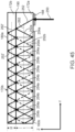
- the thickness t of the primary waveguide 172a is three times the thickness ⁇ t of the secondary waveguide 172b.
- the IC element 168 couples the in-coupled light beam 252 into the waveguide 172, which propagates within the waveguide 172 via TIR along an internally reflective optical path parallel to the axis 262 (y-axis).
- the semi-reflective interface 190 is configured for splitting the in-coupled light beam 252 into three in-coupled light beamlets.
- the semi-reflective interface 190 splits the in-coupled light beam 252 into three primary in-coupled light beamlets 252 (a first primary in-coupled light beamlet 252a (shown by a solid line) and two more primary in-coupled light beamlets 252b, 252c (shown by dashed lines)) that propagate within the primary waveguide 172a along respective internally reflective optical paths parallel to the axis 262. As shown in Fig.
- the thickness of the primary waveguide 172a is a multiple of the thickness of the secondary waveguide 172b (in this case, exactly three times as thick), only three primary in-coupled light beamlets 252a, 252b, 252c are generated due to recombination of light beamlets.
- an additional primary in-coupled light beamlet 252 is generated at each point of intersection between a secondary in-coupled light beamlet 252' and the semi-reflective interface 190, and likewise, an additional secondary in-coupled light beamlet 252' is generated at each point of intersection between a primary in-coupled light beamlet 252 and the semi-reflective interface 190.
- the number of primary in-coupled light beamlets 252 geometrically increases from the ICO 168 along the axis 262 (y-axis).
- the OPE element 186 is configured for respectively splitting the primary in-coupled light beamlets 252a-252c into three sets of primary orthogonal light beamlets.
- the primary in-coupled light beamlets 252a-252c intersect the OPE element 186 adjacent the face 180b of the waveguide 172, such that portions of the primary in-coupled light beamlets 252a-252c are diffracted as three sets of primary orthogonal light beamlets 254a-254c that propagate within the waveguide 172 via TIR along respective internally reflective optical paths parallel to the axis 264 (x-axis).
- the semi-reflective interface 190 is configured for splitting the three sets of orthogonal light beamlets 254a-254c into nine sets of orthogonal light beamlets.
- the semi-reflective interface 190 splits the set of primary orthogonal light beamlets 254a into three sets of primary orthogonal light beamlets 254a (a first set of primary in-coupled light beamlets 254a (shown by a solid line) and two more sets of primary in-coupled light beamlets 254b, 254c (shown by dashed lines)) that propagate within the primary waveguide 172a via TIR along a respective internally reflective optical path parallel to the axis 264 (x-axis).
- a first set of primary in-coupled light beamlets 254a shown by a solid line
- two more sets of primary in-coupled light beamlets 254b, 254c shown by dashed lines
- the semi-reflective interface 190 splits the set of orthogonal light beamlets 254b into three more sets of primary orthogonal light beamlets (not shown) and the set of orthogonal light beamlets 254c into three more set of primary orthogonal light beamlets (not shown) that propagate within the primary waveguide 172a via TIR along respective internally reflective optical paths parallel to the axis 264 (x-axis).
- the thickness of the primary waveguide 172a is a multiple of the thickness of the secondary waveguide 172b (in this case, exactly three times as thick), only three primary sets of orthogonal light beamlets 254a, 254b, 254c are generated due to recombination of light beamlets.
- the EPE element 188 is configured for splitting the nine sets of orthogonal light beamlets into the set of out-coupled light beamlets 256.
- the sets of primary orthogonal light beamlets 254 (only the sets of primary orthogonal light beamlets 254a(1)-254a(3) shown) intersect the EPE element 188 adjacent the face 180b of the waveguide 172, such that portions of the primary orthogonal light beamlets 254 are diffracted as the set of out-coupled light beamlets 256 that exit the face 180b of the waveguide 172.
- the increase in the number of the in-coupled light beamlets 252 and the number of orthogonal light beamlets 254 correspondingly increases the saturation of the exit pupil 300a expanded by the display screen 110 (shown in Fig. 40B ).
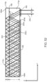
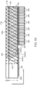
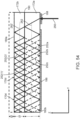
- the thickness ⁇ t of the secondary waveguide 172b can be scaled down to 3 2 the width w of the in-coupled light beam 252, so that, as illustrated in Fig. 52 , the edges of the adjacent primary in-coupled light beamlets 252 will have no gaps therebetween, and as illustrated in Fig. 53 , the edges of the adjacent primary orthogonal light beamlets 254 will have no gaps therebetween, and thus, the edges of the adjacent out-coupled light beamlets 256 will have no gaps therebetween.
- the thickness t of the primary waveguide 172a may be much larger than the width w of the collimated light beam 250 in-coupled into the waveguide apparatuses 170b, 170c, illustrated in Figs. 44-53
- the thickness ⁇ t of the secondary waveguide 172b may be smaller than the width w of the collimated light beam 250.
- the thickness of the secondary waveguide 172b may alternatively be selected, such that the difference in the thicknesses between the primary waveguide 172a and secondary waveguide 172b is equal to a difference thickness ⁇ t, as illustrated in the waveguide apparatus 170d of Figs. 54 and 55 .
- the thickness of the secondary waveguide 172b may be selected to be slightly less than the thickness t of the primary waveguide 172a, i.e., t - ⁇ t.
- the IC element 168 couples the in-coupled light beam 252 into the waveguide 172, which propagates within the waveguide 172 via TIR along an internally reflective optical path parallel to the axis 262 (y-axis).
- the semi-reflective interface 190 is configured for splitting the in-coupled light beam 252 into three in-coupled light beamlets.
- the semi-reflective interface 190 splits the in-coupled light beam 252 into three primary in-coupled light beamlets 252 (a first primary in-coupled light beamlet 252a (shown by a solid line) and two more primary in-coupled light beamlets 252b, 252c (shown by dashed lines)) that propagate within the primary waveguide 172a along respective internally reflective optical paths parallel to the axis 262. As shown in Fig.
- the semi-reflective interface 190 generates two secondary in-coupled light beamlets 252(1)' and (2)' that propagate within the secondary waveguide 172b via TIR along respective internally reflective optical paths parallel to the axis 262' (y-axis), and from which the two primary in-coupled light beamlet 252b, 252c are created.
- the OPE element 186 is configured for respectively splitting the primary in-coupled light beamlets 252a-252c into three sets of primary orthogonal light beamlets.
- the primary in-coupled light beamlets 252a-252c intersect the OPE element 186 adjacent the face 180b of the waveguide 172, such that portions of the primary in-coupled light beamlets 252a-252c are diffracted as three sets of primary orthogonal light beamlets 254a-254c that propagate within the waveguide 172 via TIR along respective internally reflective optical paths parallel to the axis 264 (x-axis).
- the semi-reflective interface 190 is configured for splitting the three sets of orthogonal light beamlets 254a-254c into nine sets of orthogonal light beamlets.
- the semi-reflective interface 190 splits the set of primary orthogonal light beamlets 254a into three sets of primary orthogonal light beamlets 254a (a first set of primary in-coupled light beamlets 254a (shown by a solid line) and two more sets of primary in-coupled light beamlets 254b, 254c (shown by dashed lines)) that propagate within the primary waveguide 172 along respective internally reflective optical paths parallel to the axis 264 (x-axis).
- a first set of primary in-coupled light beamlets 254a shown by a solid line
- two more sets of primary in-coupled light beamlets 254b, 254c shown by dashed lines
- the semi-reflective interface 190 generates two sets of secondary in-coupled light beamlets 254(1)' and 254(2)' that propagate within the secondary waveguide 172b via TIR along respective internally reflective optical paths parallel to the axis 264' (x-axis), and from which the two sets of primary in-coupled light beamlets 254b, 254c are created.
- the semi-reflective interface 190 splits the set of orthogonal light beamlets 254b into three more sets of primary orthogonal light beamlets (not shown) and the set of orthogonal light beamlets 254c into three more set of primary orthogonal light beamlets (not shown) that propagate within the primary waveguide 172a along respective internally reflective optical paths parallel to the axis 264 (x-axis).
- the EPE element 188 is configured for splitting the nine sets of orthogonal light beamlets into the set of out-coupled light beamlets 256.
- the sets of primary orthogonal light beamlets 254 (only the sets of primary orthogonal light beamlets 254a(1)-254a(3) shown) intersect the EPE element 188 adjacent the face 180b of the waveguide 172, such that portions of the primary orthogonal light beamlets 254 are diffracted as the set of out-coupled light beamlets 256 that exit the face 180b of the waveguide 172.
- the increase in the number of the in-coupled light beamlets 252 and the number of orthogonal light beamlets 254 correspondingly increases the saturation of the exit pupil 300a expanded by the display screen 110 (shown in Fig. 40B ).
- the difference thickness ⁇ t may be selected to be 3 2 the width w of the in-coupled light beam 252, so that the adjacent primary in-coupled light beamlets 252 and the edges of the adjacent primary orthogonal light beamlets 254 will have no gaps therebetween, and thus, the edges of the adjacent out-coupled light beamlets 256 will have no gaps therebetween.
- the thickness of the secondary waveguide 172b will be greater than the width w of the in-coupled light beam 252.
- waveguide apparatus 170 may have multiple secondary waveguides 172b.
- a waveguide apparatus 170e comprises two secondary waveguides 172b disposed on the primary waveguide 172a, and four semi-reflective interfaces 190, one of which is disposed between the primary waveguide 172a and one of the secondary waveguides 172b, and the remaining one of which is disposed between the respective secondary waveguides 172b.
- the IC element 168 couples the in-coupled light beam 252 into the waveguide 172, which propagates within the waveguide 172 via TIR along an internally reflective optical path parallel to the axis 262 (y-axis).
- the semi-reflective interface 190 is configured for splitting the in-coupled light beam 252 into three in-coupled light beamlets.
- the semi-reflective interfaces 190 split the in-coupled light beam 252 into three primary in-coupled light beamlets 252 (a first primary in-coupled light beamlet 252a (shown by a solid line) and two more primary in-coupled light beamlets 252b, 252c (shown by dashed lines)) that propagate within the primary waveguide 172a along respective internally reflective optical paths parallel to the axis 262 (y-axis).
- a first primary in-coupled light beamlet 252a shown by a solid line
- two more primary in-coupled light beamlets 252b, 252c shown by dashed lines
- the semi-reflective interface 190 generates two secondary in-coupled light beamlets 252' that propagate within the respective two secondary waveguides 172b via TIR along respective internally reflective optical paths parallel to the axis 262' (y-axis), and from which the two primary in-coupled light beamlet 252b, 252c are created.
- the OPE element 186 is configured for respectively splitting the primary in-coupled light beamlets 252a-252c into three sets of primary orthogonal light beamlets.
- the primary in-coupled light beamlets 252a-252c intersect the OPE element 186 adjacent the face 180b of the waveguide 172, such that portions of the primary in-coupled light beamlets 252a-252c are diffracted as three sets of primary orthogonal light beamlets 254a-254c that propagate within the waveguide 172 via TIR along internally reflective optical paths parallel to the axis 264 (x-axis).
- the semi-reflective interfaces 190 are configured for splitting the three sets of orthogonal light beamlets 254a-254c into nine sets of orthogonal light beamlets.
- the semi-reflective interfaces 190 split the set of primary orthogonal light beamlets 254a into three sets of primary orthogonal light beamlets 254a (a first set of primary orthogonal light beamlets 254a (shown by a solid line) and two more sets of primary orthogonal light beamlets 254b, 254c (shown by dashed lines)) that propagate within the primary waveguide 172a via TIR along respective internally reflective optical paths parallel to the axis 264 (x-axis).
- a first set of primary orthogonal light beamlets 254a shown by a solid line
- two more sets of primary orthogonal light beamlets 254b, 254c shown by dashed lines
- the semi-reflective interface 190 generates two sets of secondary in-coupled light beamlets 252' that propagate within the respective two secondary waveguides 172b via TIR along respective internally reflective optical paths parallel to the axis 264' (x-axis), and from which the two primary orthogonal light beamlet 252b, 252c are created.
- the semi-reflective interface 190 splits the set of orthogonal light beamlets 254b into three more sets of primary orthogonal light beamlets (not shown) and the set of orthogonal light beamlets 254c into three more set of primary orthogonal light beamlets (not shown) that propagate within the primary waveguide 172a along respective internally reflective optical paths parallel to the axis 264 (x-axis).
- the two secondary waveguides 172b may be different thicknesses.
- these different thicknesses may be non-multiples of each other. It also follows that the thickness of the primary waveguide 172a may be a non-multiple of one or both of the two different thicknesses of the two secondary waveguides 172b. In other embodiments, the two secondary waveguides 172b may be of equal thickness.
- the EPE element 188 is configured for splitting the nine sets of orthogonal light beamlets into the set of out-coupled light beamlets 256.
- the sets of primary orthogonal light beamlets 254 (only the sets of primary orthogonal light beamlets 254a(1)-254a(3) shown) intersect the EPE element 188 adjacent the face 180b of the waveguide 172, such that portions of the primary orthogonal light beamlets 254 are diffracted as the set of out-coupled light beamlets 256 that exit the face 180b of the waveguide 172.
- the increase in the number of the in-coupled light beamlets 252 and the number of orthogonal light beamlets 254 correspondingly increases the saturation of the exit pupil 300a expanded by the display screen 110 (shown in Fig. 40B ).
- the waveguide apparatus 170e illustrated in Figs. 56 and 57 has been described above as comprising two secondary waveguides 172b, it should be appreciated that waveguide apparatus 170e and others described herein may have at least two (e.g., three, four, five, or more) secondary waveguides 172b.
- the entrance pupil of the collimated light beam output by the collimation element 154 is expanded only by the combination of the OPE element 186 and EPE element 188 of the display screen 110, and includes features in close association with the OPE element 186 and EPE element 188 for increasing the saturation of the exit pupil of the display screen 110.
- the image projection assembly 108 further includes a pre-pupil expansion (PPE) 192, which in the embodiment illustrated in Fig. 58 , is disposed between the collimation element 166 and the IC element 168 of the display screen 110.
- PPE pre-pupil expansion
- the PPE 192 represents the first pupil expansion stage, and is designed to use one or more beam-multiplication techniques to pre-expand the entrance pupil of the collimated light beam 250 to an intermediate exit pupil 300a of a set (in this case, a two-dimensional 3 x 3 array) of initial out-coupled light beamlets 256' prior to in-coupling into the waveguide apparatus 170 of the display screen 110 (which emulates inputting a conventional collimated light beam having a larger pupil size as illustrated in Fig.
- the display screen 110 represents the second pupil expansion stage, which further expands, in a conventional manner, the pupil size of the collimated light beam 250 to a final exit pupil 300b of a set (in this case, a two-dimensional 9 x 9 array) of final out-coupled light beamlets 256, as illustrated in Fig. 59B .
- the display screen 110 may further expand the pupil size of the collimated light beam 250 to an exit pupil of an even more saturated set of final out-coupled light beamlets 256 using the aforementioned enhanced beam multiplication techniques.
- the use of the PPE 192 lends itself well to miniature-scale image devices that output relatively small pupil sized light beams that can be expanded to normal pupil sized light beams for input into a conventional PE for expansion to an exit pupil commensurate with the entrance pupil size of the eye(s) 52 of the end user 50.
- the PPE 192 may expand the entrance pupil of a collimated beam to a pre-expanded pupil that is at least ten times larger (e.g., at least 0.5 mm pupil) than the entrance pupil (e.g., 50 mil pupil size), and the waveguide apparatus 170 of the display screen 110 may further expand the pre-expanded pupil of the collimated light beam 250 to an exit pupil that is at least ten times larger (e.g., at least 5 mm pupil) than the pre-expanded pupil of the collimated light beam 250.
- some embodiments of the display subsystem 104' utilize a conventional PE that comprises the afore-described waveguide apparatus 170 illustrated in Figs. 34-36 and a PPE 192a that, in the illustrated embodiment, takes the form of a mini-version of the waveguide apparatus 170 that is mounted to the IC element 168.
- the PPE 192a takes the form of a waveguide apparatus 170' having a size commensurate with the size of the IC element 168 of the primary waveguide apparatus 170.
- the mini-waveguide apparatus 170' comprises a planar optical waveguide 172' that takes the form of a single unitary substrate or plane of optically transparent material (as described above with respect to the waveguide 172) and one or more DOEs 174' associated with the waveguide 172' for two-dimensionally pre-expanding the effective exit pupil of a collimated light beam 250 optically coupled into the waveguide 172'.
- the PPE 192a further comprises an IC element 168' disposed on the face 180b' of the waveguide 172' for receiving the collimated light beam 250 from the collimation element 166 into the waveguide 172' via the face 180b', although in alternative embodiments, the IC element 168' may be disposed on the other face 180a' or even the edge of the waveguide 172' for coupling the collimated light beam 250 into the waveguide 172 as an in-coupled light beam.
- the DOE(s) 174' are associated with the waveguide 172' (e.g., incorporated within the waveguide 172' or abutting or adjacent one or more of the faces 180a', 180b' of the waveguide 172') for, as briefly discussed above, two-dimensionally pre-expanding the effective entrance pupil of the collimated light beam 250 optically coupled into the waveguide 172'.
- the DOE(s) 174 comprise an orthogonal pupil expansion (OPE) element 186 for splitting the in-coupled light beam 252 into a set of initial orthogonal light beamlets 254', and an exit pupil expansion (EPE) element 188' for splitting each initial orthogonal light beamlet 254' into a set of initial out-coupled light beamlets 256' that exit the face 180b' of the waveguide 172'.
- OPE orthogonal pupil expansion
- EPE exit pupil expansion
- the OPE element 186' and EPE element 188' completely overlap each other in the x-y plane, and thus, the OPE element 186' is disposed on the face 180a of the waveguide 172' and the EPE element 188' is disposed on the face 180b of the waveguide 172'.
- the OPE element 186' and EPE element 188' may not overlap at all in the x-y plane, in which case, both the OPE element 186' and EPE element 188' may be disposed on the same face 180b of the waveguide 172'.
- the OPE element 186' relays light along a first axis (horizontal or x-axis in Fig. 60 ), and pre-expands the effective exit pupil of light along a second axis (vertical or y-axis in Fig. 60 ).
- the IC element 168' optically in-couples the collimated light beam 250 as an in-coupled light beam 252' for propagation within the waveguide 172' via TIR along an internally reflective optical path 262 (in this case, along the vertical or y-axis), and in doing so, repeatedly intersects the OPE element 186'.
- the OPE element 186' has a relatively low diffraction efficiency (e.g., less than 50%), and comprises a series of diagonal diffractive elements (forty-five degrees relative to the x-axis), such that, at each point of intersection with the OPE element 186', a portion (e.g., greater than 90%) of the in-coupled light beam 252' continues to propagate within the waveguide 172' via TIR along an internally reflective optical path parallel to the axis 262 (y-axis), and the remaining portion (e.g., less than 10%) of the in-coupled light beam 252' is diffracted as an initial orthogonal light beamlet 254' (shown as being dashed in Fig.
- a relatively low diffraction efficiency e.g., less than 50%
- a portion e.g., greater than 90%
- the remaining portion e.g., less than 10%
- axis 264 that propagates within the waveguide 172' via TIR along an internally reflective optical path parallel to the axis 264 (in this case, along the horizontal or x-axis) toward the EPE element 188'.
- the axis 264 may alternatively be obliquely oriented with respect to the axis 262.
- the entrance pupil of the collimated light beam 250 in-coupled into the mini-waveguide apparatus 170' is pre-expanded vertically along the y-axis by the OPE element 186'.
- the EPE element 188' further pre-expands the light's effective pupil along the first axis (horizontal x-axis in Fig. 62 ).
- the EPE element 188' like the OPE element 186', has a relatively low diffraction efficiency (e.g., less than 50%), such that, at each point of intersection with the EPE element 188', a portion (e.g., greater than 90%) of each initial orthogonal light beamlet 254' continues to propagate along a respective internally reflective optical path parallel to the axis 264 (x-axis), and the remaining portion of each initial orthogonal light beamlet 254' is diffracted as an initial out-coupled light beamlet 256' that exits the face 180b' of the waveguide 172' (along the z-axis), as illustrated in Fig.
- each initial orthogonal light beamlet 254' into multiple initial out-coupled light beamlets 256', the exit pupil of the in-coupled light beam 252 is further pre-expanded horizontally along the x-axis by the EPE element 188', resulting in a two-dimensional array of initial out-coupled light beamlets 256' that resemble a larger version of the original in-coupled light beam 252.
- the primary waveguide apparatus 170 further two-dimensionally expands the pupil of the collimated light beam 250. That is, the initial out-coupled light beamlets 256' are input into the IC element 168 of the primary waveguide apparatus 170 as in-coupled light beamlets 252(1)-252(4), which are in turn, split by the OPE element 186 into four sets of orthogonal light beamlets 254(1)-254(4), which are further split by the EPE element 188 into final out-coupled light beamlets 256 that exit the face 180b of the waveguide 172 towards the eye(s) 52 of the end user 50.
- a single collimated light beam 250 is split into a one-dimensional array of four initial orthogonal light beamlets 254' by the OPE element 186', which is further split into a two-dimensional 4 x 4 array of initial out-coupled light beamlets 256' by the EPE element 188', which is further split into a two-dimensional 4 x 16 array of orthogonal light beamlets 254 by the OPE element 174', which is further split into a 16 x 16 array of final out-coupled light beamlets 256.
- the use of the PPE 192a increases the saturation of the exit pupil of the display screen 110 from a 4 x 4 array of final out-coupled light beamlets 256 to a 16 x 16 array of final out-coupled light beamlets 256.
- the PPE 192a can be designed to create smaller or larger arrays of initial out-coupled light beamlets 256', e.g., a 2 x 2 array, 3 x 3 array, 5 x 5 array, etc., and can even be designed to create a non-square matrix of initial out-coupled light beamlets 256', e.g., a 2 x 3 array, 3 x 2 array, 3 x 4 array, 4 x 3 array, etc.
- the thickness of the waveguide 172 of the primary waveguide apparatus 170 will be greater than the thickness of the waveguide 172'of the mini-waveguide apparatus 170'.
- the thickness of the primary waveguide 172 is four times the thickness of the secondary waveguide 172'.
- FIG. 64-66 another embodiment of a display subsystem 104' utilizes a conventional PE that comprises the afore-described waveguide apparatus 170 illustrated in Figs. 34-36 and a PPE 192b that, like the PPE 192a, two-dimensionally pre-expanding the effective entrance pupil of a collimated light beam 250 optically coupled into the PPE 192b, but unlike the PPE 192a, is not a waveguide, but rather takes the form of an adapter.
- a conventional PE that comprises the afore-described waveguide apparatus 170 illustrated in Figs. 34-36 and a PPE 192b that, like the PPE 192a, two-dimensionally pre-expanding the effective entrance pupil of a collimated light beam 250 optically coupled into the PPE 192b, but unlike the PPE 192a, is not a waveguide, but rather takes the form of an adapter.
- the PPE 192b comprises a diffractive beam splitter 194 that utilizes a single DOE that splits the collimated light beam 250 into a set of initial out-coupled light beamlets 256'.
- the diffractive beam splitter 194 comprises an optical planar substrate 196 having opposing first and second faces 196a, 196b and a diffraction grating 198 associated with the one of the faces 196a, 196b, and in this case, the face 196b of the substrate 196.
- the diffraction grating 198 splits the collimated light beam 250 entering the face 196a of the substrate 196 into a set of diverging light beamlets 254' that exit the face 196b of the substrate 196 at diverging angles.
- the diffraction grating 198 can be designed to generate an odd number of diverging light beamlets 254' from the single collimated light beam 250 or an even number of diverging light beamlets 254' from the single collimated light beam 250.
- beamlets are created at different diffraction orders. For example, as illustrated in Fig.
- one diffraction grating 198' is designed to split the collimated light beam 250 into five diverging light beamlets 254' respectively corresponding to five diffraction orders (-2, -1, 0, +1, +2), each diverging light beamlet 254' being separated from an adjacent diverging light beamlet 254' by a separation angle ⁇ s .
- another diffraction grating 198" is designed to split the collimated light beam 250 into four diverging light beamlets 254' respectively corresponding to four diffraction orders (-3, -1, +1, +3), each diverging light beamlet 256' being separated from an adjacent diverging light beamlet 256' by a separation angle 2 ⁇ s .
- the diffraction grating 198 may either split the collimated light beam 250' into a one-dimensional array of diverging light beamlets 254' or a two-dimensional (M x N) array of diverging light beamlets 254'. In the embodiment illustrated in Figs. 64-66 , the diffraction grating splits the collimated light beam 250 into a 4 x 4 array of diverging light beamlets 254'.
- the PPE 192b can be designed to create smaller or larger arrays of diverging light beamlets 254', e.g., a 1 x 2 array, 2 x 1 array, 2 x 2 array, 3 x 3 array, 5 x 5 array, etc., and can even be designed to create non-square two-dimensional arrays of diverging light beamlets 254', e.g., a 2 x 3 array, 3 x 2 array, 3 x 4 array, 4 x 3 array, etc.
- the PPE 192b applies an angle preserving expansion to the collimated light beam 250. That is, the PPE 192b bends the set of diverging light beamlets 254' exiting the face 196b of the substrate 196 back to the original angle of the collimated light beam 250'.
- the PPE 192b comprises a lens 200, and in this embodiment a diffractive lens, that refocuses the diverging light beamlets 254' as the set of initial out-coupled light beamlets 256' back to the original angle of the collimated light beam 250'.
- the diffractive lens 200 is illustrated as being separate from the IC element 168, the function of the diffractive lens 200 can be incorporated into the IC element 168.
- the PPE 192b two-dimensionally pre-expands the effective entrance pupil of the collimated light beam 250.
- the primary waveguide apparatus 170 further two-dimensionally expands the pupil of the collimated light beam 250.
- the 4 x 4 array of initial out-coupled light beamlets 256' are input into the IC element 168 of the primary waveguide apparatus 170 as a 4 x 4 array of in-coupled light beamlets 252 (only 252(1)-252(4) shown), which are in turn, split by the OPE element 186 into a 4 x 4 array of orthogonal light beamlets 254 (only 254(1)-254(4) shown), which are further split by the EPE element 188 into final out-coupled light beamlets 256 that exit the face 180b of the waveguide 172 towards the eye(s) 52 of the end user 50, as illustrated in Figs. 64-66 .
- the separation angle 2 ⁇ s in Fig. 67B will be selected, such that the separation distance s between adjacent initial out-coupled light beamlets 256' at the intersection with the lens 200 will be equal to the desired spacings of the final out-coupled light beamlets 256 exiting the primary waveguide apparatus 170.
- a display subsystem 104 utilizes a conventional PE that comprises the afore-described waveguide apparatus 170 illustrated in Figs. 34-36 and a PPE 192c that, like the PPE 192a, two-dimensionally pre-expands the effective exit pupil of a collimated light beam 250 optically coupled into the PPE 192c, but unlike the PPE 192a, is not a waveguide, but rather takes the form of a prism.
- the PPE 192c comprises an optically transparent prism body 202, which, in the illustrated embodiment, takes the form of cuboid having a first face 202a and a second face 202b, and a plurality of prism planes 204 disposed in the interior of the prism body 202.
- the plurality of prism planes 204 comprises a first set of parallel prism planes 204a disposed at an oblique angle to the first face 202a (in this case, at a forty-five degree angle) and a second set of parallel prism planes 204b at an oblique angle to the second face 202b (in this case, at a forty-five degree angle).
- the first set of parallel prism planes 204a consists of two prism planes 202a(1) and 202a(2)
- the second set of parallel prism planes 204b consists of two prism planes 202b(1) and 202b(2), although in alternative embodiments, each set of parallel prism planes 204 may consist of more than two prism planes.
- the prism body 202 comprises prism sections 206a-202f that are bonded together to create the whole of the prism body 202.
- the prism plane 204a(1) is formed at the interface between the prism sections 206a and 206b; the prism plane 204a(2) is formed at the interface between the prism sections 206b and 206c; the prism plane 204b(1) is formed at the interface between the prism sections 206d and 206e; and the prism plane 204b(2) is formed at the interface between the prism sections 206e and 206f.
- the prism planes 204 are configured for splitting a collimated light beam 250 entering the first face 202a of the prism body 202 into a set of initial out-coupled light beamlets 256' (and in this case, a 2 x 2 array of light beamlets 256') that exit the second face 202b of the prism body 202.
- each of the prism planes 204a(1) and 204b(1) is formed of a semi-reflective coating, such as one composed of, e.g., a metal, such as gold, aluminum, silver, nickel-chromium, chromium, etc., a dielectric, such as oxides, fluorides, sulfides, etc., a semiconductor, such as silicon, germanium, etc., and/or a glue or adhesive with reflective properties, which can be disposed between adjacent prism sections 206 via any suitable process, such as physical vapor deposition (PVD), ion-assisted deposition (IAD), ion beam sputtering (IBS), etc.
- PVD physical vapor deposition
- IAD ion-assisted deposition
- IBS ion beam sputtering
- the ratio of reflection to transmission of the semi-reflective coating may be selected or determined based at least in part upon the thickness of the coating, or the semi-reflective coating may have a plurality of small perforations to control the ratio of reflection to transmission.
- each of the prism planes 204a(1) and 204b(1) will split a light beam by reflecting a portion of the light beam and transmitted the remaining portion of the light beam.
- each of the prism planes 204a(2) and 204b(2) is preferably formed of a completely reflective coating, which may be composed of the same material as the semi-reflective coating.
- the thickness of the coating may be selected, such that the prism planes 204a(2) and 204b(2) are completely reflective.
- adjacent prism sections 206 may be composed of materials having different indices of refraction, such that the prism plane 204 between the respective prism sections 206 is semi-reflective (in the case of prism planes 204a(1) or 204b(1)) or completely reflective (in the case of prism planes 204a(2) and 204b(2)) for light that is incident on the semi-reflective interface at less than a critical angle.
- each prism plane 204 is preferably designed, such that the angle of a light beam incident on the prism plane 204 is preserved.
- the first set of prism planes 204a relay light along a first axis (horizontal or x-axis), and pre-expands the effective exit pupil of light along a second axis (vertical or y-axis).
- the first set of prism planes 204a split the collimated light beam 250 entering the first face 202a of the prism body 202 into two orthogonal light beamlets 254(1)' and 254(2)', and reflects these light beamlets 254' toward the second set of prism planes 204b in a first direction.
- a portion of the collimated light beam 250 is reflected by the prism plane 204a(1) as the orthogonal light beamlet 254(1)', and the remaining portion of the collimated light beam 250 is transmitted by the prism plane 204a(1) to the prism plane 204a(2) for reflection as the orthogonal light beamlet 254(2)'.
- the second set of prism planes 204b further pre-expand the light's effective exit pupil along the second axis (horizontal or x-axis).
- the second set of prism planes 204b split each of the orthogonal light beamlets 254' into two initial out-coupled light beamlets 256', and reflects these initial out-coupled light beamlets 256' out of the second face 202b of the prism body 202 in a second direction orthogonal to the first direction, although the second direction may be non-orthogonal to the first direction.
- a portion of the orthogonal light beamlet 254(1)' is reflected by the prism plane 204b(1) as an initial out-coupled light beamlet 256(1)', and the remaining portion of the orthogonal light beamlet 254(1)' is transmitted by the prism plane 204b(1) to the prism plane 204b(2) for reflection as an initial out-coupled light beamlet 256(2)'.
- a portion of the orthogonal light beamlet 254(2)' is reflected by the prism plane 204b(1) as an initial out-coupled light beamlet 256(3)', and the remaining portion of the orthogonal light beamlet 254(2)' is transmitted by the prism plane 204b(1) to the prism plane 204b(2) for reflection as an initial out-coupled light beamlet 256(4)'.
- a 2 x 2 array of initial out-coupled light beamlets 256' exit the second face 202b of the prism body 202.
- the PPE 192c two-dimensionally pre-expands the effective entrance pupil of the collimated light beam 250.
- the primary waveguide apparatus 170 further two-dimensionally expands the pupil of the collimated light beam 250.
- the initial out-coupled light beamlets 256' are input into the IC element 168 of the primary waveguide apparatus 170 as a 2 x 2 array of in-coupled light beamlets (only 252(1)-252(2) shown), which are in turn, split by the OPE element 186 into four sets of orthogonal light beamlets (only 254(1)-254(2) shown), which are further split by the EPE element 188 into final out-coupled light beamlets 256 that exit the face 180b of the waveguide 172 towards the eye(s) 52 of the end user 50, as illustrated in Figs. 68-70 .
- the distance d between the prism planes 204 are preferably selected, such that the distance s between adjacent initial out-coupled light beamlets 256' will be equal to the desired spacings of the final out-coupled light beamlets 256 exiting the primary waveguide apparatus 170.
- the thickness of the waveguide 172 in the primary waveguide apparatus 170 can be multiples of the distance d between the prism planes 204 in each set of parallel prism planes 204 of the PPE 192c (in this case, two times the distance d between the parallel prism planes 204), such that the in-fill of final out-coupled light beamlets 256 is facilitated.
- larger arrays of initial out-coupled light beamlets 256' may be created by decreasing the distance between the prism planes 204 in each set of parallel prism planes 204 of the PPE 192c relative to the size of the prism body 202, as illustrated in Figs. 74 and 75 .
- the first set of prism planes 204a may split the collimated light beam 250 entering the first face 202a of the prism body 202 into three orthogonal light beamlets 254(1)'-254(3)', and reflects these light beamlets 254' toward the second set of prism planes 204b.
- a portion of the collimated light beam 250 is reflected by the prism plane 204a(1) as the orthogonal light beamlet 254(1)', and the remaining portion of the collimated light beam 250 is transmitted by the prism plane 204a(1) to the prism plane 204a(2), where it is repeatedly reflected between the prism plane 204a(1) and 204a(2), portions of which will be transmitted back through the prism plane 204a(1) as the orthogonal light beamlets 254(2)' and 254(3)'.
- the second set of prism planes 204b split each of the orthogonal light beamlets 254' into three initial out-coupled light beamlets 256', and reflects these initial out-coupled light beamlets 256' out of the second face 202b of the prism body 202.
- a 3 x 3 array of initial out-coupled light beamlets 256' exit the second face 202b of the prism body 202.
- each orthogonal light beamlet 254 is reflected by the prism plane 204b(1) as an initial out-coupled light beamlet 256(1)', and the remaining portion of this orthogonal light beamlet 254' is transmitted by the prism plane 204b(1) to the prism plane 204b(2), where it is repeatedly reflected between the prism plane 204b(1) and 204b(2), portions of which will be transmitted back through the prism plane 204b(1) as the initial out-coupled light beamlets 256(2)' and 256(3)'.
- the distance d between the prism planes 204 are preferably selected, such that the distance s between adjacent initial out-coupled light beamlets 256' will be equal to the desired spacings of the final out-coupled light beamlets 256 exiting the primary waveguide apparatus 170.
- each orthogonal light beamlet 254 three initial out-coupled light beamlets 256' will be generating, thereby creating a 3 x 3 array of initial out-coupled light beamlets 256' exit the second face 202b of the prism body 202.
- the PPE 192c can be designed to create even larger arrays of initial out-coupled light beamlets 256', e.g., a 4 x 4 array, a 5 x 5 array, etc., by further decreasing the distance between the prism planes 204 in each set of parallel prism planes 204 of the PPE 192c relative to the size of the prism body 202.
- the PPE 192c has been described as generated square arrays of initial out-coupled light beamlets 256', the PPE 192c can alternatively be designed to generate non-square arrays of initial out-coupled light beamlets 256', e.g., a 2 x 3 array, 3 x 2 array, 2 x 3 array, 3 x 2 array, etc., by making the distance between the prism planes 204a(1) and 204a(2) different from the distance between the prism planes 204b(1) and 204b(2).
- the PPE 192c has been described as creating two-dimensional arrays of initial out-coupled light beamlets 256', the PPE 192c can be designed to create one-dimensional arrays of initial out-coupled light beamlets 256', e.g., 1 x 2 array, 1 x 3 array, etc., by designing the PPE 192c with only one set of parallel prism planes 204.
- the PPE 192c has been described as generating initial out-coupled light beamlets 256' that exit the prism body 202 at an orthogonal angle to the face 202b of the prism body 202
- the PPE 192c can be designed, such that the initial out-coupled light beamlets 256' exit the prism body 202 at an oblique angle to the face 202b of the prism body 202 by changing the orientations of one or both of the sets of prism planes 204 relative to the face 202b of the prism body 202.
- yet another embodiment of a display subsystem 104' utilizes a conventional PE that comprises the afore-described waveguide apparatus 170 illustrated in Figs. 34-36 and a PPE 192e that, like the PPE 192c, takes the form of a prism, but unlike the PPE 192c, utilizes a cavity prism, as opposed to a solid prism, that one-dimensionally pre-expands the effective entrance pupil of a collimated light beam 250 optically coupled into the PPE 192e.
- the PPE 192e comprises an optically transparent cavity prism 208, which includes a first triangular prism section 210a and a second triangular prism section 210b.
- the prism sections 210a, 210b are spaced from each other to create an open space 212 therebetween that is bound on one side by a prism plane 212a of the prism section 210a and on the other side by a prism plane 212b of the prism section 210b, with the prism planes 212a, 212b being parallel to each other.
- the first prism section 210a has a first face 214a and a second face 214b opposite the prism plane 212a.
- the prism plane 212a is disposed at an oblique angle to the first and second faces 214a, 214b (in this case, at a forty-five degree angle).
- the PPE 192e can be designed to create smaller or larger one-dimensional arrays of initial out-coupled light beamlets 256', e.g., a 1 x 2 array, a 1 x 3 array, 1 x 5 array, etc., by decreasing or increasing the distance between the prism planes 212 relative to the size of the prism 208.
- the PPE 192e one-dimensionally pre-expands the effective entrance pupil of the collimated light beam 250.
- the primary waveguide apparatus 170 further two-dimensionally expands the pupil of the collimated light beam 250.
- the initial out-coupled light beamlets 256' are input into the IC element 168 of the primary waveguide apparatus 170 as a 1 x 4 array of in-coupled light beamlets 252(1)-252(4), which are in turn, split by the OPE element 186 into a 1 x 4 array of orthogonal light beamlets 254(1)-254(4), which are further split by the EPE element 188 into final out-coupled light beamlets 256 that exit the face 180b of the waveguide 172 towards the eye(s) 52 of the end user 50, as illustrated in Figs. 76-78 .
- the distance d between the prism planes 212 are preferably selected, such that the distance s between adjacent initial out-coupled light beamlets 256' will be equal to the desired spacings of the final out-coupled light beamlets 256 exiting the primary waveguide apparatus 170.
- the thickness of the waveguide 172 in the primary waveguide apparatus 170 will be multiples of the distance d between the prism planes 212 of the PPE 192e (in this case, two times the distance d between the prism planes 212), such that the in-fill of the final out-coupled light beamlets 256 is facilitated.
- the spacings between the final out-coupled light beamlets 256 may be arbitrarily set without concern for manufacturing limitations. That is, since the PPE 192e does not utilize an optical substrate between the prism planes 212, but rather utilizes a cavity between the prism planes 212, one need not be concerned with the limitations related to the minimum thickness of such optical substrate.
- a display subsystem 104 utilize a conventional PE that comprises the afore-described waveguide apparatus 170 illustrated in Figs. 34-36 and a PPE 192f that, in the illustrated embodiment, takes the form of a multi-layered mini-waveguide apparatus 220 mounted to the IC element 168.
- the mini-waveguide apparatus 220 has a size commensurate with the size of the IC element 168 of the primary waveguide apparatus 170.
- the mini-waveguide apparatus 220 comprises a plurality of waveguide assemblies 222, and in this case, a top waveguide assembly 222a and a bottom waveguide assembly 222b.
- Each waveguide assembly 222 is configured for splitting each of one or more collimated beams or beamlets (collimated light beam 250 in the bottom waveguide assembly 222b and out-coupled light beamlets 256' in the top waveguide assembly 222b) a two-dimensional array (in this case, a 4 x 4 array) of out-coupled light beamlets 256', as will be described in further detail below.
- the bottom waveguide assembly 222b functions to split a single collimated light beam 250 into a two-dimensional array of out-coupled light beamlets 256'
- the top waveguide assembly 222a functions to split the two-dimensional array of out-coupled light beamlets 256' from the bottom waveguide assembly 222b into multiple two-dimensional arrays of out-coupled light beamlets 256", as illustrated in Fig. 83
- the top waveguide assembly 222a and bottom waveguide assembly 222b are disposed relative to each other, such that the top waveguide assembly 222a receives the out-coupled light beamlets 256' from the bottom waveguide assembly 222b.
- the top surface 224a of the bottom waveguide assembly 222b is affixed to the bottom surface 224b of the top waveguide assembly 222a.
- each waveguide assembly 222 comprises a pair of orthogonal waveguide units configured as a top orthogonal waveguide unit 226a and a bottom orthogonal waveguide unit 226b, with the bottom surface 228b of the top orthogonal waveguide unit 226a being affixed to the top surface 228a of the bottom orthogonal waveguide unit 226b.
- the orthogonal waveguide units 226 are identical to each other, the only difference being that they are orthogonally oriented relative to each other.
- Each orthogonal waveguide unit 226 comprises a planar optical waveguide 230 taking the form of a single unitary substrate or plane of optically transparent material (as described above with respect to the waveguide 172).
- planar optical waveguides 230 of the respective orthogonal waveguide units 226 are identically dimensioned, each having top and bottom faces 230a, 230b.
- Each orthogonal waveguide unit 226 further comprises an IC element 232 associated with (e.g., disposed on) the bottom face 230b of the respective planar optical waveguide 230, and an EPE 234 respectively associated with (e.g., disposed on) the top face 230a of the planar optical waveguide 230.
- Each IC element 232 is configured for in-coupling one or more light beams or beamlets into the respective planar optical waveguide 230 for propagation via TIR along an internally reflective optical path (236a in the case of the top orthogonal waveguide unit 226a, and 236b in the case of the bottom orthogonal waveguide unit 226b), and in doing so, repeatedly intersects the EPE element 234.
- the EPE element 234 has a relatively low diffraction efficiency (e.g., less than 50%), such that, at each point of intersection with the EPE element 234, a portion (e.g., greater than 90%) of each light beam or beamlet continues to propagate along the respective internally reflective optical path 236, and the remaining portion of each light beam or beamlet is diffracted as an initial out-coupled light beamlet 256' that exits the top face 230a of the respective planar optical waveguide 230.
- a relatively low diffraction efficiency e.g., less than 50%
- the sizes of the IC element 232 and EPE element 234 are equal to each other and are commensurate to the size of the respective planar optical waveguide 230 with which the IC element 232 and EPE element 234 are associated, such that pupil expansion of the collimated light beam 250 is maximized, while also facilitating in-coupling of two-dimensional arrays of out-coupled light beamlets 256' from the bottom orthogonal waveguide unit 226b to the top orthogonal waveguide unit 226a, as will be described in further detail below.
- the IC elements 232 of the orthogonal waveguide units 226 are oriented orthogonally to each other, such that each light beam or beamlet (250 or 256') that is in-coupled into the bottom face 224b of a respective waveguide assembly 222 is split into a two-dimensional array of initial out-coupled light beamlets 256' (or 256") that exit the top face 224a of the waveguide assembly 222, as illustrated in Fig. 84 .
- each waveguide assembly 222 is oriented orthogonally relative to each other, such that the IC element 232 associated with the bottom orthogonal waveguide unit 226b in-couples light for propagation via TIR along an internally reflective optical path parallel to a first axis 262 (in this case, along the y-axis), such that the light is expanded by the corresponding EPE element 234 along the first axis 262 (see Fig.
- the IC element 232 associated with the top orthogonal waveguide unit 226a in-couples each light beam or beamlet for propagation via TIR along internally reflective optical path parallel to a second axis 264 (in this case, along the x-axis) orthogonal to the first axis 264, such that the light is expanded by the corresponding EPE element 234 along that second axis 264 (see Fig. 85A ).
- the bottom face 224b of the top waveguide assembly 222a is affixed to the top surface 224a of the bottom waveguide assembly 222b, such that the output of the bottom waveguide assembly 222a is provided as an input to the top waveguide assembly 222a, thereby generating multiple arrays of out-coupled light beamlets 256" from a single collimated light beam 250.
- the bottom waveguide assembly 222b receives the collimated light beam 250 from the collimation element 166 and splits the collimated light beam 250 into a two-dimensional array of initial out-coupled light beamlets 256' that exit the top face 224a of the bottom waveguide assembly 222b.
- the IC element 224 associated with the bottom orthogonal waveguide unit 226b of the bottom waveguide assembly 222b optically couples the collimated light beam 250 as an initial in-coupled light beam 252' for propagation within the respective planar optical waveguide 230 via TIR along the first internally reflective optical path parallel to the axis 262 (y-axis), and the EPE element 226 associated with the bottom orthogonal waveguide unit 226b of the bottom waveguide assembly 222b splits the collimated light beam 250 into a one-dimensional array of initial out-coupled light beamlets 256' that exit the top face 228a of the respective bottom orthogonal waveguide unit 226b.
- the IC element 224 associated with the top orthogonal waveguide unit 226a of the bottom waveguide assembly 222b optically couples the one-dimensional array of initial out-coupled light beamlets 256' as initial orthogonal light beamlets 254' for propagation within the respective planar optical waveguide 230 via TIR along respective second internally reflective optical paths parallel to the axis 264 (x-axis) that are orthogonal to first internally reflective optical path parallel to the axis 262 (y-axis), and the EPE element 226 associated with the top orthogonal waveguide unit 226a of the bottom waveguide assembly 222b splits the initial orthogonal light beamlets 254' into a two-dimensional array of initial out-coupled light beamlets 256' that exit the top face 228a of the respective top orthogonal waveguide unit 226a.
- the top waveguide assembly 222a receives the two-dimensional array of initial out-coupled light beamlets 256' from the bottom waveguide assembly 222b and splits this two-dimensional array of initial out-coupled light beamlets 256' into a plurality of two-dimensional arrays of intermediate out-coupled light beamlets 256" that exit the top face 224a of the top waveguide assembly 222a.
- the IC element 224 associated with the bottom orthogonal waveguide unit 226b of the top waveguide assembly 222a optically couples the two-dimensional array of initial out-coupled light beamlets 256' as intermediate sets of in-coupled light beams 252" for propagation within the respective planar optical waveguide 230 via TIR along the first internally reflective optical path parallel to the axis 262 (y-axis), and the EPE element 226 associated with the bottom orthogonal waveguide unit 226b of the top waveguide assembly 222a splits the intermediate sets of in-coupled light beamlets 252" into two-dimensional arrays of intermediate out-coupled light beamlets 256" of initial out-coupled light beamlets 256' that exit the top face 228a of the respective bottom orthogonal waveguide unit 226b.
- the IC element 224 associated with the top orthogonal waveguide unit 226a of the top waveguide assembly 222a optically couples the two-dimensional arrays of intermediate out-coupled light beamlets 256" as intermediate orthogonal light beamlets 254" for propagation within the respective planar optical waveguide 230 via TIR along respective second internally reflective optical paths 264 (x-axis) that are orthogonal to first internally reflective optical path parallel to the axis 262 (y-axis), and the EPE element 226 associated with the top orthogonal waveguide unit 226a of the top waveguide assembly 222a splits the intermediate orthogonal light beamlets 254" into two-dimensional arrays of intermediate out-coupled light beamlets 256" that exit the top face 228a of the respective top orthogonal waveguide unit 226a.
- the bottom waveguide assembly 222b splits the collimated light beam 250 into a two-dimensional array of initial out-coupled light beamlets 256'
- the top waveguide assembly 222a splits the two-dimensional array of out-coupled light beamlets 256' into several two-dimensional arrays of intermediate out-coupled light beamlets 256".
- the two-dimensional array of initial out-coupled light beamlets 256', as well as each of the two-dimensional arrays of intermediate out-coupled light beamlets 256", have an inter-beamlet spacing s1, and the two-dimensional array of intermediate out-coupled light beamlets 256" have an inter-array spacing s2 different from the inter-beamlet spacing s1 of the two-dimensional arrays of initial out-coupled light beamlets 256' and intermediate out-coupled light beamlets 256" (see, e.g., Figs. 89A and 89B ).
- the inter-array spacing s2 and the inter-beamlet spacing s1 are non-multiples of each other, so that the light beamlets 256" are distributed in a manner that maximizes the density of the in-fill of the exit pupil of the PPE 192f, and thus, the exit pupil of the display screen 110, as will be described in further detail below.
- the inter-beamlet spacing s1 is dictated by the respective thicknesses of the waveguides 230 of the bottom waveguide assembly 222b.
- the inter-array spacing s2 is dictated by the respective thicknesses of the waveguides 240 of the top waveguide assembly 222a.
- the thicknesses of the waveguides 230 of the top and bottom waveguide assemblies 222 may be strategically selected based on the diameter of the collimated light beam 250.
- the inter-beamlet spacing s1 and inter-array spacing s2 although different from each other, may each be a multiple of the diameter of the collimated light beam 250 to maximize the in-fill of the exit pupil of the PPE 192f.
- the inter-beamlet spacing s1 may be three times the diameter of the diameter of the collimated light beam 250.
- the inter-array spacing s2 may be four times the diameter of the collimated light beam 250. As exemplified in the illustrated embodiment below, this results in the inter-array spacing s2 being 1.33 times the inter-beamlet spacing s1.
- the first and second planar optical waveguide assemblies 222a, 222b respectively have unequal thicknesses t1, t2, as illustrated in Fig. 83 , with such thicknesses being set by the thicknesses of the respective planar optical waveguides 230 incorporated into the respective orthogonal waveguide units 226a, 226b of the optical waveguide assemblies 222a, 222b.
- the thicknesses of the planar optical waveguides 230 incorporated into the top planar optical waveguide assembly 222a are greater than the thicknesses of the planar optical waveguides 230 incorporated into the bottom planar optical waveguide assembly 222b.
- the first and second inter-beamlet spacing s1, s2, and thus, the thicknesses t1, t2 of the first and second planar optical waveguide assemblies 222a, 222b, are non-multiples of each other to ensure that the multiple arrays of the intermediate out-coupled light beamlets 252" are generated from the single array of initial out-coupled light beamlets 252'.
- the bottom waveguide assembly 222b splits the collimated light beam 250 into a two-dimensional array of initial out-coupled light beamlets 256'
- the top waveguide assembly 222a splits the two-dimensional array of out-coupled light beamlets 256' into several two-dimensional arrays of intermediate out-coupled light beamlets 256".
- the bottom waveguide assembly 222b and top waveguide assembly 222a respectively generate two transfer functions that are convolved to produce the desired pattern of intermediate out-coupled light beamlets 252".
- the transfer function h 1 results in a 4 x 4 array of light beamlets of a diameter a, spaced apart from each other by a distance of 3a.
- the transfer function h 2 results in a 4 x 4 array of light beamlets of a diameter a, spaced apart from each other by a distance of 4a.
- the collimated light beam 250 (as the optical input x) may be input into the bottom waveguide assembly 222b, which applies the transfer function h1 to the collimated light beam 250, thereby generating a two-dimensional array of intermediate out-coupled light beamlets 256' that have the beam pattern illustrated in Fig. 87A .
- the two-dimensional array of intermediate out-coupled light beamlets 256' output by the bottom waveguide assembly 222b may be input into the top waveguide assembly 222a, which applies the transfer function h2 to the two-dimensional array of intermediate out-coupled light beamlets 256', thereby generating multiple two-dimensional arrays of intermediate out-coupled light beamlets 256", the composite of which creates the light beamlet pattern illustrated in Fig. 87C .
- each beamlet in the 4 x 4 array of beamlets 256' that is output by the bottom waveguide assembly 222b (the first expander) illustrated in Fig. 87A , and is input into the top waveguide assembly 222a (the second expander) illustrated in Fig. 87B corresponds to a different alphabetical letter ("A" through "P").
- each beamlet 256" that is output by top waveguide assembly 222a (the second expander) can be seen as corresponding to both a specific two-dimensional array of intermediate out-coupled light beamlets 256(1)"-256(16)" and a family of related beamlets ("A" through "P").
- the two-dimensional array of intermediate out-coupled light beamlets 256(1)" is generated directly from the two-dimensional array of initial out-coupled light beamlets 256' (see Fig. 89A ).
- the two-dimensional array of intermediate out-coupled light beamlets 256(1)" spawns a two-dimensional array of intermediate out-coupled light beamlets 256(2)" and a two-dimensional array of intermediate out-coupled light beamlets 256(3)" respectively along the x-axis and the y-axis (see Fig. 89B ).
- the two-dimensional array of intermediate out-coupled light beamlets 256(2)" spawns a two-dimensional array of intermediate out-coupled light beamlets 256(4)" along the x-axis; both the two-dimensional arrays of intermediate out-coupled light beamlets 256(2)" and 256(3)” combine to spawn the two-dimensional array of intermediate out-coupled light beamlets 256(5)" respectively along the x-axis and the y-axis; ; and the two-dimensional array of intermediate out-coupled light beamlets 256(3)” spawns a two-dimensional array of intermediate out-coupled light beamlets 256(6)" along the y-axis (see Fig. 89C ).
- the two-dimensional array of intermediate out-coupled light beamlets 256(4)" spawns a two-dimensional array of intermediate out-coupled light beamlets 256(7)"along the x-axis; both the two-dimensional arrays of intermediate out-coupled light beamlets 256(4)” and 256(5)” combine to spawn the two-dimensional array of intermediate out-coupled light beamlets 256(8)" respectively along the x-axis and the y-axis; both the two-dimensional arrays of intermediate out-coupled light beamlets 256(5)” and 256(6)” combine to spawn the two-dimensional array of intermediate out-coupled light beamlets 256(9)" respectively along the x-axis and the y-axis; and the two-dimensional array of intermediate out-coupled light beamlets 256(6)” spawns a two-dimensional array of intermediate out-coupled light beamlets 256(10)" along the y-axis (see Fig. 89D ).
- both the two-dimensional arrays of intermediate out-coupled light beamlets 256(7)" and 256(8)” combine to spawn a two-dimensional array of intermediate out-coupled light beamlets 256(11)" respectively along the x-axis and the y-axis; both the two-dimensional arrays of intermediate out-coupled light beamlets 256(8)” and 256(8)” combine to spawn a two-dimensional array of intermediate out-coupled light beamlets 256(12)” respectively along the x-axis and the y-axis; and both the two-dimensional arrays of intermediate out-coupled light beamlets 256(9)” and 256(10)” combine to spawn a two-dimensional array of intermediate out-coupled light beamlets 256(13)" respectively along the x-axis and the y-axis (see Fig. 89E ).
- both the two-dimensional arrays of intermediate out-coupled light beamlets 256(11)" and 256(12)” combine to spawn a two-dimensional array of intermediate out-coupled light beamlets 256(14)" respectively along the x-axis and the y-axis; and both the two-dimensional arrays of intermediate out-coupled light beamlets 256(12)” and 256(13)” combine to spawn a two-dimensional array of intermediate out-coupled light beamlets 256(15)" respectively along the x-axis and the y-axis (see Fig. 89F ).
- the both the two-dimensional arrays of intermediate out-coupled light beamlets 256(14)" and 256(15)" combine to spawn a two-dimensional array of intermediate out-coupled light beamlets 256(16)" respectively along the x-axis and the y-axis (see Fig. 89G ).
- a 4 x 4 array of intermediate out-coupled light beamlets 256" designated with the letter “D” can be derived from the single initial out-coupled light beamlet 256a designed with the letter “D.”
- a 4 x 4 array of intermediate out-coupled light beamlets 256" designated with the letter “M” can be derived from the single initial out-coupled light beamlet 256a designed with the letter “M.”
- a 4 x 4 array of intermediate out-coupled light beamlets 256" designated with the letter "P” can be derived from the single initial out-coupled light beamlet 256a designed with the letter "P.”
- the PPE 192f two-dimensionally pre-expands the effective entrance pupil of the collimated light beam 250.
- the primary waveguide apparatus 170 further two-dimensionally expands the pupil of the collimated light beam 250.
- the intermediate out-coupled light beamlets 256" are input into the IC element 168 of the primary waveguide apparatus 170 as in-coupled light beamlets 252, which are in turn, split by the OPE element 186 into orthogonal light beamlets 254, which are further split by the EPE element 188 into final out-coupled light beamlets 256 that exit the face 180b of the waveguide 172 towards the eye(s) 52 of the end user 50, as illustrated in Figs. 80-82 .
- the primary waveguide apparatus 170 may be designed to assume that the PPE 192f has an exit pupil consisting of only the 10 x 10 two-dimensional array of out-coupled beamlets 258'.
- the multi-layered mini-waveguide apparatus 220 lends itself for use as a PPE 192f
- a larger version of the multi-layered waveguide apparatus 220 can be used as the primary waveguide apparatus 170 in order to expand the entrance pupil of a collimated light beam 250 (unexpanded or pre-expanded) in-coupled into the primary waveguide apparatus 170.
- beam multipliers have been described above as OPEs and EPEs, beam multipliers according to the embodiments described herein can be disposed anywhere in an LOE. For instance, beam multipliers described herein can be disposed as a separate multiplication stage/region between various parts of an LOE (e.g., between ICG and OPE). Further, beam multipliers described herein can function as ICGs.
- each single beam or beamlet depicted in the figures may represent a plurality of beams or beamlets carrying related information and having similar trajectories.
- MR systems are provided as examples of various optical systems that can benefit from more selectively reflective optical elements. Accordingly, use of the optical systems described herein is not limited to the disclosed MR systems, but rather applicable to any optical system.
- the disclosure includes methods that may be performed using the subject devices.
- the methods may comprise the act of providing such a suitable device. Such provision may be performed by the end user.
- the "providing" act merely requires the end user obtain, access, approach, position, set-up, activate, power-up or otherwise act to provide the requisite device in the subject method.
- Methods recited herein may be carried out in any order of the recited events which is logically possible, as well as in the recited order of events.
- any optional feature of the inventive variations described may be set forth and claimed independently, or in combination with any one or more of the features described herein.
- Reference to a singular item includes the possibility that there are plural of the same items present. More specifically, as used herein and in claims associated hereto, the singular forms “a,” “an,” “said,” and “the” include plural referents unless the specifically stated otherwise.
- use of the articles allow for "at least one" of the subject item in the description above as well as claims associated with this disclosure.
- claims may be drafted to exclude any optional element. As such, this statement is intended to serve as antecedent basis for use of such exclusive terminology as “solely,” “only” and the like in connection with the recitation of claim elements, or use of a “negative” limitation.
Landscapes
- Physics & Mathematics (AREA)
- General Physics & Mathematics (AREA)
- Optics & Photonics (AREA)
- Engineering & Computer Science (AREA)
- General Engineering & Computer Science (AREA)
- Computer Hardware Design (AREA)
- Computer Graphics (AREA)
- Software Systems (AREA)
- Theoretical Computer Science (AREA)
- Optical Couplings Of Light Guides (AREA)
- Diffracting Gratings Or Hologram Optical Elements (AREA)
- Controls And Circuits For Display Device (AREA)
- Eyeglasses (AREA)
- Processing Or Creating Images (AREA)
Applications Claiming Priority (4)
| Application Number | Priority Date | Filing Date | Title |
|---|---|---|---|
| US201762506841P | 2017-05-16 | 2017-05-16 | |
| US201762509499P | 2017-05-22 | 2017-05-22 | |
| PCT/US2018/032883 WO2018213388A1 (en) | 2017-05-16 | 2018-05-16 | Systems and methods for mixed reality |
| EP18803279.1A EP3625616B1 (de) | 2017-05-16 | 2018-05-16 | Systeme und verfahren für gemischte realität |
Related Parent Applications (2)
| Application Number | Title | Priority Date | Filing Date |
|---|---|---|---|
| EP18803279.1A Division-Into EP3625616B1 (de) | 2017-05-16 | 2018-05-16 | Systeme und verfahren für gemischte realität |
| EP18803279.1A Division EP3625616B1 (de) | 2017-05-16 | 2018-05-16 | Systeme und verfahren für gemischte realität |
Publications (2)
| Publication Number | Publication Date |
|---|---|
| EP4579312A2 true EP4579312A2 (de) | 2025-07-02 |
| EP4579312A3 EP4579312A3 (de) | 2025-08-06 |
Family
ID=64274867
Family Applications (2)
| Application Number | Title | Priority Date | Filing Date |
|---|---|---|---|
| EP25176717.4A Pending EP4579312A3 (de) | 2017-05-16 | 2018-05-16 | Systeme und verfahren für gemischte realität |
| EP18803279.1A Active EP3625616B1 (de) | 2017-05-16 | 2018-05-16 | Systeme und verfahren für gemischte realität |
Family Applications After (1)
| Application Number | Title | Priority Date | Filing Date |
|---|---|---|---|
| EP18803279.1A Active EP3625616B1 (de) | 2017-05-16 | 2018-05-16 | Systeme und verfahren für gemischte realität |
Country Status (9)
| Country | Link |
|---|---|
| US (6) | US10755481B2 (de) |
| EP (2) | EP4579312A3 (de) |
| JP (4) | JP7104722B2 (de) |
| KR (4) | KR102753311B1 (de) |
| CN (2) | CN110678802B (de) |
| AU (2) | AU2018270948B2 (de) |
| CA (1) | CA3061377A1 (de) |
| IL (2) | IL308323B2 (de) |
| WO (1) | WO2018213388A1 (de) |
Families Citing this family (36)
| Publication number | Priority date | Publication date | Assignee | Title |
|---|---|---|---|---|
| AU2018270948B2 (en) * | 2017-05-16 | 2022-11-24 | Magic Leap, Inc. | Systems and methods for mixed reality |
| US11422369B1 (en) | 2017-06-14 | 2022-08-23 | Meta Platforms Technologies, Llc | Multi-layered substrates for waveguide displays |
| GB2566274A (en) * | 2017-09-06 | 2019-03-13 | Wave Optics Ltd | Display for use in an augmented reality or virtual reality device |
| KR102096928B1 (ko) * | 2017-12-18 | 2020-04-03 | 삼성전자주식회사 | 광학 시스템 및 이를 구비한 웨어러블 표시장치 |
| WO2019170954A1 (en) * | 2018-03-07 | 2019-09-12 | Nokia Technologies Oy | An apparatus for use in a near eye display |
| US11125993B2 (en) * | 2018-12-10 | 2021-09-21 | Facebook Technologies, Llc | Optical hyperfocal reflective systems and methods, and augmented reality and/or virtual reality displays incorporating same |
| US11150394B2 (en) * | 2019-01-31 | 2021-10-19 | Facebook Technologies, Llc | Duty cycle range increase for waveguide combiners |
| EP3926389B1 (de) * | 2019-04-01 | 2024-05-22 | Lg Chem, Ltd. | Streulichtführungsplatte und anzeigevorrichtung damit |
| CN114207354B (zh) * | 2019-09-16 | 2024-06-21 | 鲁姆斯有限公司 | 具有光束倍增的图像显示系统 |
| US11958183B2 (en) | 2019-09-19 | 2024-04-16 | The Research Foundation For The State University Of New York | Negotiation-based human-robot collaboration via augmented reality |
| KR102601442B1 (ko) * | 2019-10-07 | 2023-11-13 | 주식회사 엘지화학 | 홀로그래픽 도광판 |
| EP4053615B1 (de) * | 2019-11-01 | 2025-10-22 | Letinar Co., Ltd | Kompakte optische vorrichtung der erweiterten realität mit geisterbildblockierfunktion und weitem betrachtungswinkel |
| WO2021202746A1 (en) * | 2020-04-03 | 2021-10-07 | Magic Leap, Inc. | Wearable display systems with nanowire led micro-displays |
| JP7585351B2 (ja) | 2020-05-22 | 2024-11-18 | マジック リープ, インコーポレイテッド | 相関内部結合および外部結合光学領域を伴う拡張および仮想現実ディスプレイシステム |
| WO2022086002A1 (en) | 2020-10-20 | 2022-04-28 | Samsung Electronics Co., Ltd. | Waveguide structure with segmented diffractive optical elements and near-eye display apparatus employing the same |
| US11886022B2 (en) | 2020-11-06 | 2024-01-30 | Samsung Electronics Co., Ltd. | Beam expander and beam expansion method |
| EP4015899B1 (de) * | 2020-12-15 | 2024-09-04 | Micledi Microdisplays BV | Optimierung der strahlformung für lichtemittierende anzeigen |
| EP4067974B1 (de) * | 2021-03-29 | 2025-06-04 | Optinvent | 2d-pupillenexpandierende lichtleiteranordnung |
| FR3121236B1 (fr) | 2021-03-29 | 2024-02-09 | Optinvent | Guide optique et procede de fabrication correspondant |
| JP7651237B2 (ja) * | 2021-03-31 | 2025-03-26 | パナソニックオートモーティブシステムズ株式会社 | 導光板 |
| WO2022209106A1 (ja) | 2021-03-31 | 2022-10-06 | パナソニックIpマネジメント株式会社 | 導光板、導光板ユニット、および、表示装置 |
| KR102627824B1 (ko) * | 2021-08-11 | 2024-01-23 | 주식회사 레티널 | 회절 소자를 이용한 증강 현실용 광학 장치 |
| US20230045957A1 (en) * | 2021-08-12 | 2023-02-16 | Facebook Technologies, Llc | Multi-source light-guiding illuminator |
| US20240248312A1 (en) * | 2021-09-15 | 2024-07-25 | Vuzix Corporation | Imaging light guide apparatus with light security |
| CN114167601B (zh) * | 2021-11-10 | 2022-11-18 | 北京灵犀微光科技有限公司 | 一种三次扩瞳装置 |
| US12196976B2 (en) | 2021-12-28 | 2025-01-14 | Meta Platforms Technologies, Llc | Multi-directional gratings in a waveguide system |
| US12242060B2 (en) * | 2022-02-08 | 2025-03-04 | Optinvent | Multi-pupil expansion light guide assembly with rod |
| TWI848278B (zh) * | 2022-03-28 | 2024-07-11 | 赫旺國際股份有限公司 | 浮空投影操作裝置、浮空投影裝置及其全像光學模組 |
| CN120188084A (zh) * | 2022-10-31 | 2025-06-20 | 奇跃公司 | 用于可见光谱具有两个或多个分离反射和透射ic光瞳的双有源层波导架构 |
| CN115657314B (zh) * | 2022-11-09 | 2024-03-22 | 中国科学院长春光学精密机械与物理研究所 | 基于光场波前相位调制的ar衍射光波导装置 |
| US12613418B2 (en) | 2022-12-16 | 2026-04-28 | Apple Inc. | Display devices with bridge emitters and sensors |
| CN116430603A (zh) * | 2023-03-02 | 2023-07-14 | 中山大学 | 基于一维发散光束的光波导显示模组 |
| US11892640B1 (en) * | 2023-03-07 | 2024-02-06 | Microsoft Technology Licensing, Llc | Waveguide combiner with stacked plates |
| CN118112812B (zh) * | 2024-04-23 | 2024-07-02 | 北京灵犀微光科技有限公司 | 一种阵列光波导组及近眼显示设备 |
| DE102024205613A1 (de) * | 2024-06-18 | 2025-12-18 | Robert Bosch Gesellschaft mit beschränkter Haftung | Wellenleitvorrichtung für eine Datenbrille, Datenbrille und Verfahren zum Betreiben einer Wellenleitvorrichtung |
| CN118764603B (zh) * | 2024-09-09 | 2024-12-10 | 武汉精立电子技术有限公司 | Ned设备双目清晰度调整、mtf一致性补偿方法及装置 |
Family Cites Families (70)
| Publication number | Priority date | Publication date | Assignee | Title |
|---|---|---|---|---|
| JPS6095313A (ja) * | 1983-10-31 | 1985-05-28 | Toshiba Corp | 形状測定装置 |
| JP2759635B2 (ja) * | 1996-01-17 | 1998-05-28 | 郵政省通信総合研究所長 | 非回折光ビーム発生方法及び装置 |
| JP2004045684A (ja) | 2002-07-11 | 2004-02-12 | Sony Corp | 画像表示装置における照明光学装置及び画像表示装置 |
| JP4055548B2 (ja) | 2002-10-28 | 2008-03-05 | ソニー株式会社 | 画像表示装置における照明光学装置及び画像表示装置 |
| EP1639394A2 (de) | 2003-06-10 | 2006-03-29 | Elop Electro-Optics Industries Ltd. | Verfahren und system zum anzeigen eines informativen bildes vor einem hintergrundbild |
| GB0314444D0 (en) * | 2003-06-20 | 2003-07-23 | Univ Heriot Watt | Novel wavefront sensor |
| US7418170B2 (en) * | 2004-03-29 | 2008-08-26 | Sony Corporation | Optical device and virtual image display device |
| WO2006025317A1 (ja) | 2004-08-31 | 2006-03-09 | Nikon Corporation | 光束径拡大光学系及び画像表示装置 |
| US7206107B2 (en) | 2004-12-13 | 2007-04-17 | Nokia Corporation | Method and system for beam expansion in a display device |
| JP2006276198A (ja) | 2005-03-28 | 2006-10-12 | Brother Ind Ltd | ヘッドマウント型画像表示装置 |
| EP1922579B1 (de) | 2005-09-07 | 2015-08-19 | BAE Systems PLC | Projektionsanzeige mit zwei plattenartigen coplanaren, gitter enthaltenden wellenleitern |
| JP2007219106A (ja) | 2006-02-16 | 2007-08-30 | Konica Minolta Holdings Inc | 光束径拡大光学素子、映像表示装置およびヘッドマウントディスプレイ |
| WO2008081070A1 (en) | 2006-12-28 | 2008-07-10 | Nokia Corporation | Device for expanding an exit pupil in two dimensions |
| EP3667399A1 (de) | 2007-06-04 | 2020-06-17 | Magic Leap, Inc. | Diffraktiver strahlaufweiter |
| US7589901B2 (en) * | 2007-07-10 | 2009-09-15 | Microvision, Inc. | Substrate-guided relays for use with scanned beam light sources |
| US8369019B2 (en) | 2008-04-14 | 2013-02-05 | Bae Systems Plc | Waveguides |
| JP4518193B2 (ja) * | 2008-06-10 | 2010-08-04 | ソニー株式会社 | 光学装置および虚像表示装置 |
| GB0902468D0 (en) * | 2009-02-16 | 2009-04-01 | Light Blue Optics Ltd | Optical systems |
| US8194325B2 (en) * | 2009-06-30 | 2012-06-05 | Nokia Corporation | Optical apparatus and method |
| JP5104823B2 (ja) | 2009-07-29 | 2012-12-19 | 株式会社島津製作所 | 表示装置 |
| US8649099B2 (en) * | 2010-09-13 | 2014-02-11 | Vuzix Corporation | Prismatic multiple waveguide for near-eye display |
| CN102033319B (zh) * | 2010-10-25 | 2015-07-15 | 北京理工大学 | 一种应用全息元件的视度型显示装置 |
| US10156722B2 (en) | 2010-12-24 | 2018-12-18 | Magic Leap, Inc. | Methods and systems for displaying stereoscopy with a freeform optical system with addressable focus for virtual and augmented reality |
| US8531773B2 (en) | 2011-01-10 | 2013-09-10 | Microvision, Inc. | Substrate guided relay having a homogenizing layer |
| US8548290B2 (en) * | 2011-08-23 | 2013-10-01 | Vuzix Corporation | Dynamic apertured waveguide for near-eye display |
| WO2013033274A1 (en) * | 2011-08-29 | 2013-03-07 | Vuzix Corporation | Controllable waveguide for near-eye display applications |
| JP5901192B2 (ja) | 2011-09-13 | 2016-04-06 | オリンパス株式会社 | 光学機構 |
| FR2983976B1 (fr) | 2011-12-13 | 2017-10-20 | Optinvent | Guide optique a elements de guidage superposes et procede de fabrication |
| EP2842003B1 (de) * | 2012-04-25 | 2019-02-27 | Rockwell Collins, Inc. | Holographisches weitwinkeldisplay |
| US8989535B2 (en) * | 2012-06-04 | 2015-03-24 | Microsoft Technology Licensing, Llc | Multiple waveguide imaging structure |
| US9671566B2 (en) | 2012-06-11 | 2017-06-06 | Magic Leap, Inc. | Planar waveguide apparatus with diffraction element(s) and system employing same |
| US9019615B2 (en) | 2012-06-12 | 2015-04-28 | Microsoft Technology Licensing, Llc | Wide field-of-view virtual image projector |
| JP5984591B2 (ja) | 2012-09-05 | 2016-09-06 | オリンパス株式会社 | 表示方法及び表示装置 |
| JP6510160B2 (ja) | 2012-10-22 | 2019-05-08 | セイコーエプソン株式会社 | 光学デバイス及び画像表示装置 |
| US9933684B2 (en) | 2012-11-16 | 2018-04-03 | Rockwell Collins, Inc. | Transparent waveguide display providing upper and lower fields of view having a specific light output aperture configuration |
| CN105229719B (zh) | 2013-03-15 | 2018-04-27 | 奇跃公司 | 显示系统和方法 |
| WO2015006784A2 (en) | 2013-07-12 | 2015-01-15 | Magic Leap, Inc. | Planar waveguide apparatus with diffraction element(s) and system employing same |
| DE102013219625B3 (de) * | 2013-09-27 | 2015-01-22 | Carl Zeiss Ag | Brillenglas für eine auf den Kopf eines Benutzers aufsetzbare und ein Bild erzeugende Anzeigevorrichtung sowie Anzeigevorrichtung mit einem solchen Brillenglas |
| US9857591B2 (en) | 2014-05-30 | 2018-01-02 | Magic Leap, Inc. | Methods and system for creating focal planes in virtual and augmented reality |
| KR102651578B1 (ko) | 2013-11-27 | 2024-03-25 | 매직 립, 인코포레이티드 | 가상 및 증강 현실 시스템들 및 방법들 |
| JP6287131B2 (ja) * | 2013-12-02 | 2018-03-07 | セイコーエプソン株式会社 | 虚像表示装置 |
| JP6413291B2 (ja) * | 2014-03-27 | 2018-10-31 | セイコーエプソン株式会社 | 虚像表示装置、およびヘッドマウントディスプレイ |
| JP6442149B2 (ja) * | 2014-03-27 | 2018-12-19 | オリンパス株式会社 | 画像表示装置 |
| GB2526092A (en) | 2014-05-13 | 2015-11-18 | Nokia Technologies Oy | An apparatus and method for providing an image |
| NZ764905A (en) * | 2014-05-30 | 2022-05-27 | Magic Leap Inc | Methods and systems for generating virtual content display with a virtual or augmented reality apparatus |
| IL296027B2 (en) * | 2014-05-30 | 2024-08-01 | Magic Leap Inc | Methods and system for creating focal planes in virtual and augmented reality |
| CN111856755B (zh) | 2014-05-30 | 2022-07-19 | 奇跃公司 | 用于显示虚拟和增强现实的立体视觉的方法和系统 |
| US20160077338A1 (en) * | 2014-09-16 | 2016-03-17 | Steven John Robbins | Compact Projection Light Engine For A Diffractive Waveguide Display |
| EP3198192A1 (de) * | 2014-09-26 | 2017-08-02 | Milan Momcilo Popovich | Optischer tracker mit holografischem wellenleiter |
| AU2015323940B2 (en) * | 2014-09-29 | 2021-05-20 | Magic Leap, Inc. | Architectures and methods for outputting different wavelength light out of waveguides |
| JP6417589B2 (ja) | 2014-10-29 | 2018-11-07 | セイコーエプソン株式会社 | 光学素子、電気光学装置、装着型表示装置および光学素子の製造方法 |
| US9575316B2 (en) | 2014-10-29 | 2017-02-21 | Google Inc. | Simplified mirror |
| FR3030790B1 (fr) | 2014-12-19 | 2017-02-10 | Commissariat Energie Atomique | Dispositif optique de projection pour des moyens d'affichage tels que des lunettes a realite augmentee. |
| WO2016105285A1 (en) * | 2014-12-26 | 2016-06-30 | Koc University | Near-to-eye display device with variable resolution |
| CN204687853U (zh) * | 2015-03-20 | 2015-10-07 | 京东方科技集团股份有限公司 | 一种车载显示系统和汽车 |
| JP6519256B2 (ja) | 2015-03-23 | 2019-05-29 | セイコーエプソン株式会社 | 光束径拡大素子および表示装置 |
| IL256276B (en) * | 2015-06-15 | 2022-09-01 | Magic Leap Inc | Display system with optical components for coupling multiple light streams |
| AU2016296723B2 (en) | 2015-07-20 | 2021-03-04 | Magic Leap, Inc. | Collimating fiber scanner design with inward pointing angles in virtual/augmented reality system |
| US10007117B2 (en) | 2015-09-10 | 2018-06-26 | Vuzix Corporation | Imaging light guide with reflective turning array |
| WO2017062483A1 (en) | 2015-10-05 | 2017-04-13 | Magic Leap, Inc. | Microlens collimator for scanning optical fiber in virtual/augmented reality system |
| WO2017060665A1 (en) * | 2015-10-05 | 2017-04-13 | Milan Momcilo Popovich | Waveguide display |
| IL304501B2 (en) | 2015-10-06 | 2024-08-01 | Magic Leap Inc | A virtual/augmented reality system with an inverted angle refraction grating |
| JP6597196B2 (ja) | 2015-11-05 | 2019-10-30 | セイコーエプソン株式会社 | 虚像表示措置 |
| US9791696B2 (en) * | 2015-11-10 | 2017-10-17 | Microsoft Technology Licensing, Llc | Waveguide gratings to improve intensity distributions |
| US10359627B2 (en) * | 2015-11-10 | 2019-07-23 | Microsoft Technology Licensing, Llc | Waveguide coatings or substrates to improve intensity distributions having adjacent planar optical component separate from an input, output, or intermediate coupler |
| WO2017176861A1 (en) | 2016-04-07 | 2017-10-12 | Magic Leap, Inc. | Systems and methods for augmented reality |
| US10025093B2 (en) * | 2016-04-13 | 2018-07-17 | Microsoft Technology Licensing, Llc | Waveguide-based displays with exit pupil expander |
| JP2018054673A (ja) | 2016-09-26 | 2018-04-05 | セイコーエプソン株式会社 | 網膜走査型表示装置およびビーム径拡大素子 |
| CN110023819B (zh) | 2016-11-30 | 2022-05-17 | 奇跃公司 | 用于高分辨率数字显示的方法和系统 |
| AU2018270948B2 (en) | 2017-05-16 | 2022-11-24 | Magic Leap, Inc. | Systems and methods for mixed reality |
-
2018
- 2018-05-16 AU AU2018270948A patent/AU2018270948B2/en active Active
- 2018-05-16 CN CN201880034011.8A patent/CN110678802B/zh active Active
- 2018-05-16 KR KR1020247021428A patent/KR102753311B1/ko active Active
- 2018-05-16 US US15/980,947 patent/US10755481B2/en active Active
- 2018-05-16 EP EP25176717.4A patent/EP4579312A3/de active Pending
- 2018-05-16 EP EP18803279.1A patent/EP3625616B1/de active Active
- 2018-05-16 CA CA3061377A patent/CA3061377A1/en active Pending
- 2018-05-16 IL IL308323A patent/IL308323B2/en unknown
- 2018-05-16 IL IL270459A patent/IL270459B2/en unknown
- 2018-05-16 WO PCT/US2018/032883 patent/WO2018213388A1/en not_active Ceased
- 2018-05-16 JP JP2019563122A patent/JP7104722B2/ja active Active
- 2018-05-16 KR KR1020197036766A patent/KR102365138B1/ko active Active
- 2018-05-16 CN CN202111339558.9A patent/CN114019685A/zh active Pending
- 2018-05-16 KR KR1020227005055A patent/KR102586582B1/ko active Active
- 2018-05-16 KR KR1020237033436A patent/KR102680658B1/ko active Active
-
2020
- 2020-06-16 US US16/903,279 patent/US11107288B2/en active Active
-
2021
- 2021-07-30 US US17/389,684 patent/US11651566B2/en active Active
-
2022
- 2022-04-26 JP JP2022072295A patent/JP7483785B2/ja active Active
-
2023
- 2023-02-22 AU AU2023201026A patent/AU2023201026B2/en active Active
- 2023-04-05 US US18/296,141 patent/US11935206B2/en active Active
-
2024
- 2024-02-02 US US18/431,758 patent/US12277658B2/en active Active
- 2024-05-01 JP JP2024074384A patent/JP7736852B2/ja active Active
-
2025
- 2025-03-10 US US19/075,137 patent/US20250209758A1/en active Pending
- 2025-08-28 JP JP2025142227A patent/JP7839349B2/ja active Active
Also Published As
Similar Documents
| Publication | Publication Date | Title |
|---|---|---|
| AU2023201026B2 (en) | Systems and methods for mixed reality | |
| US12181682B2 (en) | Eyepieces for augmented reality display system | |
| US12306407B2 (en) | Eyepieces for augmented reality display system | |
| JP2022060344A (ja) | 仮想現実、拡張現実、および複合現実システムのための接眼レンズ | |
| CN114286962A (zh) | 用于增强现实显示系统的目镜 |
Legal Events
| Date | Code | Title | Description |
|---|---|---|---|
| PUAI | Public reference made under article 153(3) epc to a published international application that has entered the european phase |
Free format text: ORIGINAL CODE: 0009012 |
|
| STAA | Information on the status of an ep patent application or granted ep patent |
Free format text: STATUS: THE APPLICATION HAS BEEN PUBLISHED |
|
| AC | Divisional application: reference to earlier application |
Ref document number: 3625616 Country of ref document: EP Kind code of ref document: P |
|
| AK | Designated contracting states |
Kind code of ref document: A2 Designated state(s): AL AT BE BG CH CY CZ DE DK EE ES FI FR GB GR HR HU IE IS IT LI LT LU LV MC MK MT NL NO PL PT RO RS SE SI SK SM TR |
|
| PUAL | Search report despatched |
Free format text: ORIGINAL CODE: 0009013 |
|
| AK | Designated contracting states |
Kind code of ref document: A3 Designated state(s): AL AT BE BG CH CY CZ DE DK EE ES FI FR GB GR HR HU IE IS IT LI LT LU LV MC MK MT NL NO PL PT RO RS SE SI SK SM TR |
|
| RIC1 | Information provided on ipc code assigned before grant |
Ipc: G02B 27/00 20060101AFI20250702BHEP |
|
| STAA | Information on the status of an ep patent application or granted ep patent |
Free format text: STATUS: REQUEST FOR EXAMINATION WAS MADE |
|
| 17P | Request for examination filed |
Effective date: 20260205 |