EP4543178A2 - Anzeigesubstrate und anzeigevorrichtungen - Google Patents
Anzeigesubstrate und anzeigevorrichtungen Download PDFInfo
- Publication number
- EP4543178A2 EP4543178A2 EP25162388.0A EP25162388A EP4543178A2 EP 4543178 A2 EP4543178 A2 EP 4543178A2 EP 25162388 A EP25162388 A EP 25162388A EP 4543178 A2 EP4543178 A2 EP 4543178A2
- Authority
- EP
- European Patent Office
- Prior art keywords
- sub
- type
- power lines
- pixel groups
- pixels
- Prior art date
- Legal status (The legal status is an assumption and is not a legal conclusion. Google has not performed a legal analysis and makes no representation as to the accuracy of the status listed.)
- Pending
Links
Images


Classifications
-
- G—PHYSICS
- G09—EDUCATION; CRYPTOGRAPHY; DISPLAY; ADVERTISING; SEALS
- G09G—ARRANGEMENTS OR CIRCUITS FOR CONTROL OF INDICATING DEVICES USING STATIC MEANS TO PRESENT VARIABLE INFORMATION
- G09G3/00—Control arrangements or circuits, of interest only in connection with visual indicators other than cathode-ray tubes
- G09G3/20—Control arrangements or circuits, of interest only in connection with visual indicators other than cathode-ray tubes for presentation of an assembly of a number of characters, e.g. a page, by composing the assembly by combination of individual elements arranged in a matrix no fixed position being assigned to or needed to be assigned to the individual characters or partial characters
- G09G3/22—Control arrangements or circuits, of interest only in connection with visual indicators other than cathode-ray tubes for presentation of an assembly of a number of characters, e.g. a page, by composing the assembly by combination of individual elements arranged in a matrix no fixed position being assigned to or needed to be assigned to the individual characters or partial characters using controlled light sources
- G09G3/30—Control arrangements or circuits, of interest only in connection with visual indicators other than cathode-ray tubes for presentation of an assembly of a number of characters, e.g. a page, by composing the assembly by combination of individual elements arranged in a matrix no fixed position being assigned to or needed to be assigned to the individual characters or partial characters using controlled light sources using electroluminescent panels
- G09G3/32—Control arrangements or circuits, of interest only in connection with visual indicators other than cathode-ray tubes for presentation of an assembly of a number of characters, e.g. a page, by composing the assembly by combination of individual elements arranged in a matrix no fixed position being assigned to or needed to be assigned to the individual characters or partial characters using controlled light sources using electroluminescent panels semiconductive, e.g. using light-emitting diodes [LED]
- G09G3/3208—Control arrangements or circuits, of interest only in connection with visual indicators other than cathode-ray tubes for presentation of an assembly of a number of characters, e.g. a page, by composing the assembly by combination of individual elements arranged in a matrix no fixed position being assigned to or needed to be assigned to the individual characters or partial characters using controlled light sources using electroluminescent panels semiconductive, e.g. using light-emitting diodes [LED] organic, e.g. using organic light-emitting diodes [OLED]
- G09G3/3225—Control arrangements or circuits, of interest only in connection with visual indicators other than cathode-ray tubes for presentation of an assembly of a number of characters, e.g. a page, by composing the assembly by combination of individual elements arranged in a matrix no fixed position being assigned to or needed to be assigned to the individual characters or partial characters using controlled light sources using electroluminescent panels semiconductive, e.g. using light-emitting diodes [LED] organic, e.g. using organic light-emitting diodes [OLED] using an active matrix
- G09G3/3233—Control arrangements or circuits, of interest only in connection with visual indicators other than cathode-ray tubes for presentation of an assembly of a number of characters, e.g. a page, by composing the assembly by combination of individual elements arranged in a matrix no fixed position being assigned to or needed to be assigned to the individual characters or partial characters using controlled light sources using electroluminescent panels semiconductive, e.g. using light-emitting diodes [LED] organic, e.g. using organic light-emitting diodes [OLED] using an active matrix with pixel circuitry controlling the current through the light-emitting element
-
- H—ELECTRICITY
- H10—SEMICONDUCTOR DEVICES; ELECTRIC SOLID-STATE DEVICES NOT OTHERWISE PROVIDED FOR
- H10K—ORGANIC ELECTRIC SOLID-STATE DEVICES
- H10K59/00—Integrated devices, or assemblies of multiple devices, comprising at least one organic light-emitting element covered by group H10K50/00
- H10K59/10—OLED displays
- H10K59/12—Active-matrix OLED [AMOLED] displays
- H10K59/131—Interconnections, e.g. wiring lines or terminals
-
- H—ELECTRICITY
- H10—SEMICONDUCTOR DEVICES; ELECTRIC SOLID-STATE DEVICES NOT OTHERWISE PROVIDED FOR
- H10K—ORGANIC ELECTRIC SOLID-STATE DEVICES
- H10K59/00—Integrated devices, or assemblies of multiple devices, comprising at least one organic light-emitting element covered by group H10K50/00
- H10K59/30—Devices specially adapted for multicolour light emission
- H10K59/35—Devices specially adapted for multicolour light emission comprising red-green-blue [RGB] subpixels
- H10K59/353—Devices specially adapted for multicolour light emission comprising red-green-blue [RGB] subpixels characterised by the geometrical arrangement of the RGB subpixels
-
- G—PHYSICS
- G09—EDUCATION; CRYPTOGRAPHY; DISPLAY; ADVERTISING; SEALS
- G09G—ARRANGEMENTS OR CIRCUITS FOR CONTROL OF INDICATING DEVICES USING STATIC MEANS TO PRESENT VARIABLE INFORMATION
- G09G2300/00—Aspects of the constitution of display devices
- G09G2300/04—Structural and physical details of display devices
- G09G2300/0421—Structural details of the set of electrodes
- G09G2300/0426—Layout of electrodes and connections
-
- G—PHYSICS
- G09—EDUCATION; CRYPTOGRAPHY; DISPLAY; ADVERTISING; SEALS
- G09G—ARRANGEMENTS OR CIRCUITS FOR CONTROL OF INDICATING DEVICES USING STATIC MEANS TO PRESENT VARIABLE INFORMATION
- G09G2300/00—Aspects of the constitution of display devices
- G09G2300/04—Structural and physical details of display devices
- G09G2300/0439—Pixel structures
- G09G2300/0452—Details of colour pixel setup, e.g. pixel composed of a red, a blue and two green components
-
- G—PHYSICS
- G09—EDUCATION; CRYPTOGRAPHY; DISPLAY; ADVERTISING; SEALS
- G09G—ARRANGEMENTS OR CIRCUITS FOR CONTROL OF INDICATING DEVICES USING STATIC MEANS TO PRESENT VARIABLE INFORMATION
- G09G2300/00—Aspects of the constitution of display devices
- G09G2300/04—Structural and physical details of display devices
- G09G2300/0439—Pixel structures
- G09G2300/0465—Improved aperture ratio, e.g. by size reduction of the pixel circuit, e.g. for improving the pixel density or the maximum displayable luminance or brightness
Definitions
- the present application relates to the field of display technologies, and in particular, to display substrates and display devices.
- OLED display substrates have a wide range of applications in fields of smart phones, televisions, VR (Virtual Reality) devices, wearable devices, etc. due to their excellent display effect, and characteristics such as thinness, flexibility, excellent shock resistance, and suitability for wearable products.
- disposing the cameras under the display substrates places higher requirements on the performance of the display substrates, especially on their light transmittance. High light transmittance of regions for enabling the cameras to capture images on the display substrates is a basic condition for applying this solution. Therefore, how to improve the light transmittance of the display substrates is a technical problem that needs to be solved.
- the present disclosure provides display substrates and display devices.
- a display substrate including: a display region including a first display sub-region and a second display sub-region, wherein the second display sub-region adjoins the first display sub-region, and a light transmittance of the first display sub-region is higher than a light transmittance of the second display sub-region; a plurality of first-type sub-pixels located in the first display sub-region, wherein the plurality of first-type sub-pixels are divided into a plurality of sub-pixel groups and each of the plurality of sub-pixel groups includes at least two adjacent first-type sub-pixels in a row direction; each of the plurality of first-type sub-pixels includes a light emitting element and a pixel circuit configured to drive the light emitting element to emit light; and a plurality of power lines connected to the plurality of first-type sub-pixels; wherein the plurality of power lines include first-type power lines and second-type power lines, the first-type power lines extend
- a distance between two adjacent sub-pixel groups is longer than or equal to a width of at least one of the sub-pixel groups in the row direction; and in sub-pixel groups that are in a same column, a distance between two adjacent sub-pixel groups is longer than or equal to a length of at least one of the sub-pixel groups in the column direction.
- orthographic projections of sub-pixel groups in an (i+2) th row on sub-pixel groups in an i th row are located outside orthographic projections of sub-pixel groups in an (i+1) th row on the sub-pixel groups in the i th row, orthographic projections of sub-pixel groups in an (i+3) th row on the sub-pixel groups in the i th row overlaps the orthographic projections of the sub-pixel groups in the (i+1) th row on the sub-pixel groups in the i th row, and the orthographic projections of the sub-pixel groups in the (i+3) th row on the sub-pixel groups in the i th row are located outside the orthographic projections of the sub-pixel groups in the (i+2) th row on the sub-pixel groups in the i th row, where i is a positive integer; and orthographic projections of sub-pixel groups in a (j+2) th column on sub-pixel groups in a
- pixel circuits of first-type sub-pixels in a same sub-pixel group are connected to a same first-type power line, and the same first-type power line is connected to pixel circuits of first-type sub-pixels in sub-pixel groups in two adjacent rows.
- a number of second-type power lines connected to a sub-pixel group in the plurality of sub-pixel groups is smaller than a number of columns of first-type sub-pixels in the sub-pixel group.
- a number of the second-type power lines is equal to a number of columns of the plurality of sub-pixel groups; and pixel circuits of first-type sub-pixels in sub-pixel groups in a same column are connected to a same second-type power line.
- each of the plurality of sub-pixel groups includes three first-type sub-pixels that are arranged in sequence in the row direction, one first-type power line of the first-type power lines is connected with the three first-type sub-pixels and one second-type power line of the second-type power lines is connected with the first-type sub-pixel that is in a middle among the three first-type sub-pixels.
- the second-type power line is connected with the first-type sub-pixel that is in a middle among the three first-type sub-pixels.
- the three first-type sub-pixels include one red sub-pixel, one blue sub-pixel and one green sub-pixel.
- the plurality of power lines further include third-type power lines, and the third-type power lines are connected to at least one type of the first-type power lines or the second-type power lines; and a number of the third-type power lines is same as a number of the plurality of sub-pixel groups, and pixel circuits of first-type sub-pixels in each of the plurality of sub-pixel groups are connected to a same third-type power line.
- the third-type power lines are connected to the first-type power lines and the second-type power lines
- the third-type power lines include first conductive portions and second conductive portions, the first conductive portions are connected to the second conductive portions, the first conductive portions extend along the row direction, and the second conductive portions extend along the column direction
- the first-type power lines include third conductive portions, and the third conductive portions extend along the row direction
- the second-type power lines extend along the column direction
- the first conductive portions are connected to the third conductive portions
- the second-type power lines are connected to the first conductive portions or the second conductive portions
- the third-type power lines are connected to the first-type power lines
- the third-type power lines include first conductive portions, and the first conductive portions extend along the row direction
- the first-type power lines include third conductive portions, and the third conductive portions extend along the row direction
- the first conductive portions are connected to the third conductive portions.
- a sum of a number of the first-type power lines and a number of the second-type power lines is smaller than a sum of a number of rows and a number of columns of an array including the plurality of first-type sub-pixels.
- a sum of a number of the first-type power lines and a number of the second-type power lines connected with each of the sub-pixel groups is smaller than a sum of a number of rows and a number of columns of first-type sub-pixels in each of the sub-pixel groups.
- the number of the first-type power lines is equal to the number of the rows of the array including the plurality of first-type sub-pixels; and pixel circuits of first-type sub-pixels in sub-pixel groups in a same row are connected to only a same first-type power line, and the same first-type power line is connected to only pixel circuits of first-type sub-pixels in sub-pixel groups in the same row.
- the number of the second-type power lines is smaller than the number of the columns of the array including the plurality of first-type sub-pixels.
- the number of the second-type power lines is equal to 1/3 times the number of the columns of the array including the plurality of first-type sub-pixels, and the number of the second-type power lines is equal to a number of columns of the plurality of sub-pixel groups; and pixel circuits of first-type sub-pixels in sub-pixel groups in a same column are connected to a same second-type power line, and the same second-type power line is connected to pixel circuits of first-type sub-pixels in sub-pixel groups in a same column.
- the second display sub-region includes a plurality of second-type sub-pixels, and the plurality of second-type sub-pixels are arranged in an array along the row direction and the column direction; and a density of the first-type sub-pixels in the first display sub-region is smaller than a density of the second-type sub-pixels in the second display sub-region.
- the plurality of power lines further include fourth power lines and fifth power lines, the fourth power lines are connected to pixel circuits of the second-type sub-pixels arranged along the row direction, and the fifth power lines are connected to pixel circuits of the second-type sub-pixels arranged along the column direction; a density of the power lines in the first display sub-region is smaller than a density of the power lines in the second display sub-region.
- a display device including a photosensitive element and the above display substrate. Orthographic projection of the photosensitive element on the display substrate is located within the first display sub-region.
- the photosensitive element is an image sensor, an ambient light sensor or a distance sensor.
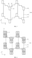
- a display substrate 1 includes a display region 11.
- the display region 11 includes a first display sub-region 111 and a second display sub-region 112.
- a light transmittance of the first display sub-region 111 is higher than that of the second display sub-region 112.
- the display substrate 1 includes: a plurality of first-type sub-pixels 21 and a plurality of power lines VDD.
- the plurality of first-type sub-pixels 21 and the plurality of power lines VDD are located in the first display sub-region 111.
- the plurality of first-type sub-pixels 21 are arranged in an array along a row direction X and a column direction Y.
- the first-type sub-pixel 21 includes a light emitting element and a pixel circuit for driving the light emitting element to emit light.
- a plurality of power lines 22 are connected to one another.
- the plurality of power lines 22 include at least one type of first-type power lines 221 or second-type power lines 222.
- the first-type power lines 221 are configured to be connected to pixel circuits of the first-type sub-pixels 21 arranged along the row direction X.
- first-type sub-pixels 21 there is at least one row of first-type sub-pixels 21 near which no first-type power lines 221 are disposed, and there is at least one column of first-type sub-pixels 21 near which no second-type power lines 222 are disposed, which can reduce the number and the occupied area of the power lines, and can be beneficial to improve the light transmittance of the first display sub-region 111.
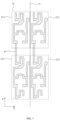
- the display substrate includes a display region.
- the display region includes a first display sub-region 111 and a second display sub-region 112.
- a light transmittance of the first display sub-region 111 is higher than that of the second display sub-region 112.
- the display substrate includes a plurality of first-type sub-pixels 21 and a plurality of power lines 22.
- the plurality of first-type sub-pixels 21 and the plurality of power lines 22 are located in the first display sub-region 111.
- the plurality of first-type sub-pixels 21 are arranged in an array along a row direction X and a column direction Y.
- Each first-type sub-pixel 21 includes a light emitting element and a pixel circuit for driving the light emitting element to emit light.
- the pixel circuit may include transistors, and may further include capacitors.
- the pixel circuit may be a 1T pixel circuit, a 2T1C pixel circuit, a 3T1C pixel circuit, a 4T1C pixel circuit, a 5T1C pixel circuit, or a 7T1C pixel circuit.
- the 7T1C pixel circuit will be taken as an example for illustration.
- each sub-pixel group 31 includes two adjacent first-type sub-pixels 21 in the row direction X, and two adjacent first-type sub-pixels 21 in the column direction Y. That is, each sub-pixel group 31 includes four first-type sub-pixels 21.
- each sub-pixel group 31 includes one red sub-pixel 211, two green sub-pixels 212 and one blue sub-pixel 213.
- the red sub-pixel 211 and the blue sub-pixel 213 may be located in the same column, and the two green sub-pixels 212 may be located in the same column, but they are not limited thereto.
- the second display sub-region 112 includes a plurality of second-type sub-pixels, and the plurality of second-type sub-pixels are arranged in an array along the row direction X and the column direction Y.
- a density of the first-type sub-pixels 21 in the first display sub-region 111 is smaller than that of the second-type sub-pixels in the second display sub-region 112.
- the density of the first-type sub-pixels 21 in the first display sub-region 111 may be 1/2 of that of the second-type sub-pixels in the second display sub-region 112.
- a distance S1 between two adjacent sub-pixel groups 31 is higher than a width W of the sub-pixel group 31 in the row direction X.
- the distance S1 between two adjacent sub-pixel groups 31 may be equal to the width W of the sub-pixel group 31 in the row direction X. In this way, the light transmittance of the first display sub-region 111 can be improved.
- a distance S2 between two adjacent sub-pixel groups 31 is equal to a length L of the sub-pixel group 31 in the column direction Y.
- the distance S2 between two adjacent sub-pixel groups 31 may be higher than the length L of the sub-pixel group 31 in the column direction Y. In this way, the light transmittance of the first display sub-region 111 can be improved.
- orthographic projections of sub-pixel groups 31 in an ( i +2) th row on sub-pixel groups 31 in an i th row are located outside orthographic projections of sub-pixel groups 31 in an ( i +1) th row on the sub-pixel groups 31 in the i th row
- orthographic projections of sub-pixel groups 31 in an ( i +3) th row on the sub-pixel groups 31 in the i th row overlaps the orthographic projections of sub-pixel groups 31 in the ( i +1) th row on the sub-pixel groups 31 in the i th row
- the orthographic projections of sub-pixel groups 31 in the ( i +3) th row on the sub-pixel groups 31 in the i th row are located outside the orthographic projections of sub-pixel groups 31 in the ( i +2) th row on the sub-pixel groups 31 in the i th row, where i is a positive integer.
- orthographic projections of sub-pixel groups 31 in a third row on sub-pixel groups 31 in a first row are located outside orthographic projections of sub-pixel groups 31 in a second row on the sub-pixel groups 31 in the first row
- orthographic projections of sub-pixel groups 31 in a fourth row on the sub-pixel groups 31 in the first row overlaps the orthographic projections of sub-pixel groups 31 in the second row on the sub-pixel groups 31 in the first row
- the orthographic projections of sub-pixel groups 31 in the fourth row on the sub-pixel groups 31 in the first row are located outside the orthographic projections of sub-pixel groups 31 in the third row on the sub-pixel groups 31 in the first row.
- orthographic projections of sub-pixel groups 31 in a ( j +2) th column on sub-pixel groups 31 in a j th column are located outside orthographic projections of sub-pixel groups 31 in a ( j +1) th column on the sub-pixel groups 31 in the j th column
- orthographic projections of sub-pixel groups 31 in a ( j +3) th column on the sub-pixel groups 31 in the j th column overlaps the orthographic projections of sub-pixel groups 31 in the ( j +1) th column on the sub-pixel groups 31 in the j th column
- the orthographic projections of sub-pixel groups 31 in the ( j +3) th column on the sub-pixel groups 31 in the j th column are located outside the orthographic projections of sub-pixel groups 31 in the ( j +2) th column on the sub-pixel groups 31 in the j th column, where j is a positive integer.
- orthographic projections of sub-pixel groups 31 in a third column on sub-pixel groups 31 in a first column are located outside orthographic projections of sub-pixel groups 31 in a second column on the sub-pixel groups 31 in the first column
- orthographic projections of sub-pixel groups 31 in a fourth column on the sub-pixel groups 31 in the first column overlaps the orthographic projections of sub-pixel groups 31 in the second column on the sub-pixel groups 31 in the first column
- the orthographic projections of sub-pixel groups 31 in the fourth column on the sub-pixel groups 31 in the first column are located outside the orthographic projections of sub-pixel groups 31 in the third column on the sub-pixel groups 31 in the first column.
- the plurality of power lines 22 are connected to one another. In this way, a resistance of the power lines can be reduced, and further, a voltage drop of power supply voltages in the column direction Y can be decreased.
- the plurality of power lines 22 include first-type power lines 221, second-type power lines 222 and third-type power lines 223.
- the first-type power lines 221, the second-type power lines 222 and the third-type power lines 223 are located in the first display sub-region 111.
- the first-type power lines 221 are configured to be connected to pixel circuits of the first-type sub-pixels 21 arranged along the row direction X.
- a number of the first-type power lines 221 is smaller than a number of rows of the array, the number of the first-type power lines 221 is equal to 0.25 time the number of rows of the array, and the number of the first-type power lines 221 is equal to 0.5 time a number of rows of the sub-pixel groups 31.
- FIG. 2 8 rows of first-type sub-pixels 21 and 4 rows of sub-pixel groups 31 are shown, and the number of first-type power lines 221 is 2.
- pixel circuits of four first-type sub-pixels 21 in the same sub-pixel group 31 are connected to just the same first-type power line 221, and the same first-type power line 221 is connected to pixel circuits of first-type sub-pixels 21 in sub-pixel groups 31 in two adjacent rows, that is, the same first-type power line 221 is connected to pixel circuits of first-type sub-pixels 21 in four adjacent rows.
- the second-type power lines 222 are configured to be connected to pixel circuits of the first-type sub-pixels 21 arranged along the column direction Y.
- a number of the second-type power lines 222 is smaller than a number of columns of the array, the number of the second-type power lines 222 is equal to 0.5 time the number of columns of the array, and the number of the second-type power lines 222 is equal to a number of columns of the sub-pixel groups 31.
- 8 columns of first-type sub-pixels 21 and 4 columns of sub-pixel groups 31 are shown, and the number of second-type power lines 222 is 4.
- pixel circuits of four first-type sub-pixels 21 in sub-pixel groups 31 in the same column are connected to the same second-type power line 222.
- the same second-type power line 222 is connected to pixel circuits of four first-type sub-pixels 21 in sub-pixel groups 31 in the same column.
- the third-type power lines 223 are connected to the first-type power lines 221 and the second-type power lines 222, and a number of the third-type power lines 223 is the same as a number of the sub-pixel groups 31. Pixel circuits of four first-type sub-pixels 21 in each sub-pixel group 31 are connected to the same third-type power line 223.
- the third-type power lines 223 may have a ring shape, for example, a rectangular ring shape, but they are not limited thereto.
- the third-type power line 223 includes a first conductive portion E1 and a second conductive portion E2.
- the first conductive portion E1 is connected to the second conductive portion E2.
- the first conductive portion E1 extends along the row direction X
- the second conductive portion E2 extends along the column direction Y.
- the first-type power line 221 includes a third conductive portion E3.
- the third conductive portion E3 extends along the row direction X
- the second-type power line 222 extends along the column direction Y.
- the first conductive portion E1 is connected to the third conductive portion E3
- a second-type power line 222 is connected to the second conductive portion E2.
- the first conductive portion E1 is connected to a second-type power line 222.
- a sum of the number of the first-type power lines 221 and the number of the second-type power lines 222 is smaller than a sum of the number of rows and the number of columns of the array. Therefore, there is at least one row of first-type sub-pixels 21 near which no first-type power lines 221 are disposed, and at least one column of first-type sub-pixels 21 near which no second-type power lines 222 are disposed, which reduces the number and an occupied area of the power lines, and is beneficial to improve the light transmittance of the first display sub-region 111.
- the plurality of power lines 22 further include fourth power lines and fifth power lines.
- the fourth power lines and the fifth power lines may be located in the second display sub-region 112.
- the first-type power lines 221, the second-type power lines 222, the third-type power lines 223, the fourth power lines, and the fifth power lines are connected to one another.
- a number of the fourth power lines is the same as a number of rows of the array. Pixel circuits of second-type sub-pixels in the same row are connected to the same fourth power line, and the same fourth power line is connected to pixel circuits of second-type sub-pixels in the same row.
- a number of the fifth source lines is the same as a number of columns of the array. Pixel circuits of second-type sub-pixels in the same column are connected to the same fifth power line, and the same fifth power line is connected to pixel circuits of second-type sub-pixels in the same column.
- a density of the power lines in the first display sub-region 111 is smaller than that in the second display sub-region 112. Since the density of the power lines in the first display sub-region 111 is smaller than that in the second display sub-region 112, the light transmittance of the first display sub-region 111 can be improved.
- FIGS. 2-4 A structure of the display substrate in this example has been shown above briefly in FIGS. 2-4 . The structure of the display substrate in the example will be further described below.
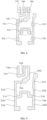
- a pixel circuit 51 is connected to a light emitting element D for driving the light emitting element D to emit light.
- the pixel circuit 51 is connected to a power line VDD, and a negative electrode of the light emitting element D is connected to a power line VSS.
- the pixel circuit 51 may include a drive transistor T1, a data writing transistor T2, a threshold compensation transistor T3, a second light emission control transistor T4, a first light emission control transistor T5, a first reset transistor T6, a second reset transistor T7 and a storage capacitor C.
- the threshold compensation transistor T3 and the first reset transistor T6 may be double-gate transistors.
- the drive transistor T1 is used to provide a drive current for the light emitting element D.
- a gate electrode of the drive transistor T1 is connected to a first electrode of the capacitor C, a first electrode of the threshold compensation transistor T3, and a second electrode of the first reset transistor T6.
- a first electrode of the drive transistor T1 is connected to a second electrode of the threshold compensation transistor T3 and a second electrode of the first light emission control transistor T5.
- a second electrode of the drive transistor T1 is connected to a first electrode of the second light emission control transistor T4 and a second electrode of the data writing transistor T2.
- a first electrode of the data writing transistor T2 is configured to be electrically connected to a data line Vd to receive data signals.
- a gate electrode of the data writing transistor T2 is electrically connected to a first scan signal line Ga1 to receive scan signals, and the first electrode of the data writing transistor T2 is electrically connected to the data line Vd to receive the data signals.
- a gate electrode of the threshold compensation transistor T3 is electrically connected to a second scan signal line Ga2 to receive compensation control signals.
- a gate electrode of the second light emission control transistor T4 is electrically connected to a first light emission control signal line EM1 to receive first light emission control signals, and a second electrode of the second light emission control transistor T4 is connected to a second electrode of the capacitor and the power line VDD.
- a gate electrode of the first light emission control transistor T5 is electrically connected to a second light emission control signal line EM2 to receive second light emission control signals, and a first electrode of the first light emission control transistor T5 is connected to a first electrode of the second reset transistor T7 and a positive electrode of the light emitting element D.
- a gate electrode of the first reset transistor T6 is electrically connected to a first reset control signal line Rst1 to receive first sub-reset control signals, and a first electrode of the first reset transistor T6 is electrically connected to a first reset power supply terminal Vinit1 to receive first reset signals.
- a gate electrode of the second reset transistor T7 is electrically connected to a second reset control signal line Rst2 to receive second sub-reset control signals, and a second electrode of the second reset transistor T7 is electrically connected to a second reset power supply terminal Vinit2 to receive second reset signals.
- the drive transistor T1, the data writing transistor T2, the threshold compensation transistor T3, the second light emission control transistor T4, the first light emission control transistor T5, the first reset transistor T6, and the second reset transistor T7 are P-type transistors, their first electrodes are source electrodes, and their second electrodes are drain electrodes.
- one or more of the drive transistor T1, the data writing transistor T2, the threshold compensation transistor T3, the second light emission control transistor T4, the first light emission control transistor T5, the first reset transistor T6, and the second reset transistor T7 may be N-type transistors.
- a voltage of power supply signals provided by the power line VDD is higher than that provided by the power line VSS.
- the voltage of the power supply signals provided by the power line VDD is a positive voltage, and the voltage of the power supply signals provided by the power line VSS may be 0 or a negative voltage.
- a voltage of power supply signals provided by the power line VSS when being grounded is 0.
- the voltage of the power supply signals provided by the power line VDD may be smaller than that provided by the power line VSS.
- the first light emission control signals may be the same as the second light emission control signals, and the gate electrode of the second light emission control transistor T4 and the gate electrode of the first light emission control transistor T5 may be connected to the same light emission control signal line EM, where the light emission control signal line EM is the first light emission control signal line EM1 or the second light emission control signal line EM2.
- the first sub-reset control signals may be the same as the second sub-reset control signals, and the gate electrode of the first reset transistor T6 and the gate electrode of the second reset transistor T7 may be connected to the same reset control signal line Rst, where the reset control signal line Rst may be the first reset control signal line Rst1 or the second reset control signal line Rst2.
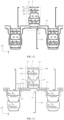
- FIGS. 6 to 14 show structures of layers of pixel circuits of 4 rows and 6 columns of first-type sub-pixels 21, or structures of layers of pixel circuits of first-type sub-pixels 21 in 2 rows and 3 columns of sub-pixel groups 31.
- FIGS. 6 to 11 show structures of an active semiconductor layer 61 in a pixel circuit.
- the active semiconductor layer 61 may be formed by patterning semiconductor material.
- the active semiconductor layer 61 may be used to manufacture active layers of drive transistors T1, data writing transistors T2, threshold compensation transistors T3, second light emission control transistors T4, first light emission control transistors T5, first reset transistors T6, and second reset transistors T7.
- An active semiconductor layer 61 includes active layer patterns and doped region patterns of transistors of the sub-pixels, where a doped region pattern includes a source region and a drain region. Active layer patterns and doped region patterns of transistors in the same pixel circuit are integrally disposed.
- a drive transistor T1 includes an active layer T1C, a source region T1S, and a drain region T1D;
- a data writing transistor T2 includes an active layer T2C, a source region T2S, and a drain region T2D;
- a threshold compensation transistor T3 includes an active layer T3C, a source region T3S, and a drain region T3D;
- a second light emission control transistor T4 includes an active layer T4C, a source region T4S, and a drain region T4D;
- a first light emission control transistor T5 includes an active layer T5C, a source region T5S, and a drain region T5D;
- a first reset transistor T6 includes an active layer T6C, a source region T6S, and a drain region T6D; and
- a second reset transistor T7 includes an active layer T7C, a source region T7S, and a drain region T7D.
- an active layer may include an integrally formed low-temperature polysilicon layer, and a source region and a drain region may be subjected to conductor processing by doping or the like to achieve electrical connection between structures. That is, an active semiconductor layer of transistors of each first-type sub-pixel 21 is an overall pattern formed of p-silicon, and each transistor in the same pixel circuit includes a doped region pattern (i.e., a source region and a drain region) and an active layer pattern. Active layers of different transistors are separated by doped structures.
- the active semiconductor layers 61 may be made of amorphous silicon, polysilicon, oxide semiconductor materials, or the like. It should be noted that the source regions and the drain regions may be regions doped with N-type or P-type impurities.
- each sub-pixel group 31 active semiconductor layers 61 are symmetrical about a symmetry axis 71, and the symmetry axis 71 extends along a column direction Y, that is, active semiconductor layers 61 of pixel circuits of a red sub-pixel 211 and a green sub-pixel 212 located in the same row are symmetrical about the symmetry axis 71, and active semiconductor layers 61 of pixel circuits of a blue sub-pixel 213 and a green sub-pixel 212 located in the same row are symmetrical about the symmetry axis 71. It should be noted that each sub-pixel group 31 is also symmetrical about the symmetry axis 71.
- FIG. 7 in each sub-pixel group 31, active semiconductor layers 61 of pixel circuits of first-type sub-pixels 21 located in the same column are connected to one another.
- active semiconductor layers 61 of pixel circuits of two first-type sub-pixels 21 located in the same column have substantially the same structure, but also have different portions.
- FIGS. 8 to 11 show a structure of an active semiconductor layer 61 of a pixel circuit of a red sub-pixel 211.
- FIGS. 10 and 11 show a structure of an active semiconductor layer 61 of a pixel circuit of a blue sub-pixel 213.
- FIG. 12 shows a structure of a first conductive layer 121 in a pixel circuit.
- the first conductive layer 121 is located on a gate insulation layer.
- the first conductive layer 121 is located on the gate insulation layer and insulated from an active semiconductor layer 61. As shown in FIG.
- the first conductive layer 121 may include a first electrode CC1 of a storage capacitor C, a first scan signal line Ga1, a reset control signal line Rst, a light emission control signal line EM, and a first vertical conductive portion 2221, and the first conductive layer 121 may include gate electrodes of a drive transistor T1, a data writing transistor T2, a threshold compensation transistor T3, a second light emission control transistor T4, a first light emission control transistor T5, a first reset transistor T6, and a second reset transistor T7.
- the first electrode CC1 of the storage capacitor C is also the gate electrode of the drive transistor T1.
- the gate electrode of the data writing transistor T2 may be a portion where the first scan signal line Ga1 overlaps the active semiconductor layer 61;
- the gate electrode of the second light emission control transistor T4 may be a first portion where the light emission control signal line EM overlaps the active semiconductor layer 61, and the gate electrode of the first light emission control transistor T5 may be a second portion where the light emission control signal line EM overlaps the active semiconductor layer 61;
- the gate electrode of the first reset transistor T6 is a first portion where the reset control signal line Rst overlaps the active semiconductor layer 61, and the gate electrode of the second reset transistor T7 is a second portion where the reset control signal line Rst overlaps the active semiconductor layer 61;
- the threshold compensation transistor T3 may be a thin film transistor with a double-gate structure, a first gate electrode of the threshold compensation transistor T3 may be a portion where the first scan signal line Ga1 overlaps the active semiconductor layer 61, and a second gate electrode of the threshold compensation transistor T3 may be a portion where a pro
- the first vertical conductive portion 2221 extends along a column direction Y, and constitutes a part of a second-type power line 222.
- the first vertical conductive portion 2221 includes connecting portions 122 for connecting with other portions of power lines through via holes.
- FIG. 13 shows a structure of a second conductive layer 131 in a pixel circuit.
- the second conductive layer 131 includes a reset signal line VINIT, a second electrode CC2 of a storage capacitor C, a second vertical conductive portion 2222, a first horizontal conductive portion 2211, a second horizontal conductive portion 2212, and a light shielding portion SHL.
- Reset signal lines VINIT of pixel circuits of all first-type sub-pixels 21 are connected together.
- a horizontal conductive portion does not refer to that the conductive portion extends along a row direction X, but is used to be connected with pixel circuits of first-type sub-pixels 21 arranged along the row direction X.
- a vertical conductive portion may refer to that the conductive portion extends along a column direction Y.
- the second vertical conductive portion 2222 includes connecting portions 132 for connecting with other portions of power lines through via holes.
- the first horizontal conductive portion 2211 includes a connecting portion 133 for connecting with the second horizontal conductive portion 2212 through a via hole
- the second horizontal conductive portion 2212 includes a connecting portion 134 for connecting with the first horizontal conductive portion 2211 through a via hole.
- FIG. 14 shows a structure of a third conductive layer 141 in a pixel circuit.
- the third conductive layer 141 includes a data line Vd, a third vertical conductive portion 2231, a fourth vertical conductive portion 2232, and connecting portions 142.
- the third vertical conductive portion 2231 and the fourth vertical conductive portion 2232 extend along a column direction Y respectively.
- the third vertical conductive portion 2231 and the fourth vertical conductive portion 2232 are second conductive portions E2.
- the third vertical conductive portion 2231 and the fourth vertical conductive portion 2232 are respectively connected to a second electrode CC2 through via holes to realize a ring-shaped structure of a third-type power line 223.
- the connecting portions 142 are respectively connected to a connecting portion 133 of the first horizontal conductive portion 2211 and a connecting portion 134 of the second horizontal conductive portion 2212 through via holes to form a first-type power line 221.
- a plurality of power lines 22 include only first-type power lines 221 and third-type power lines 223, but do not include second-type power lines 222, that is, a number of the second-type power lines 222 is 0, and a density of the first-type power lines 221 is higher than that in the above examples.
- a first-type power line 221 exists between pixel circuits of first-type sub-pixels 21 in sub-pixel groups 31 in two adjacent rows, and the pixel circuits of the first-type sub-pixels 21 in the sub-pixel groups 31 in two adjacent rows are connected to the same first-type power line 221, that is, pixel circuits of first-type sub-pixels 21 in four adjacent rows are connected to the same first-type power line 221. Also, pixel circuits of first-type sub-pixels 21 in the same sub-pixel group 31 are connected to two adjacent first-type power lines 221.
- each third-type power line 223 includes two first conductive portions E1, and the first conductive portions E1 extend along a row direction X.
- Each first-type power line 221 includes third conductive portions E3, and the third conductive portions E3 extend along the row direction X.
- First conductive portions of third-type power lines 223 are connected to third conductive portions of first-type power lines 221.
- a third-type power line 223 is respectively connected to two first-type power lines 221 through two first conductive portions.
- a density of power lines in a first display sub-region 111 is smaller than that in a second display sub-region 112. Since the density of the power lines in the first display sub-region 111 is smaller than that in the second display sub-region 112, a light transmittance of the first display sub-region 111 can be improved.
- each sub-pixel group 31 includes three adjacent first-type sub-pixels 21 in a row direction X.
- each sub-pixel group 31 includes adjacent red sub-pixel 211, green sub-pixel 212 and blue sub-pixel 213 in the row direction X.
- a density of first-type sub-pixels 21 in a first display sub-region 111 is smaller than that of second-type sub-pixels in a second display sub-region 112. In this way, a light transmittance of the first display sub-region 111 can be improved.
- a number of first-type power lines 221 is equal to a number of rows of the array. Pixel circuits of first-type sub-pixels 21 in sub-pixel groups 31 in the same row are connected to just the same first-type power line 221, and the same first-type power line 221 is connected to just pixel circuits of first-type sub-pixels 21 in sub-pixel groups 31 in the same row.
- a number of second-type power lines 222 is smaller than a number of columns of the array. In this way, the number of second-type power lines 222 can be reduced, and the light transmittance of the first display sub-region 111 can be improved.
- the number of second-type power lines 222 is equal to 1/3 times a number of columns of the array, and the number of second-type power lines 222 is equal to a number of columns of sub-pixel groups 31.
- FIG. 20 shows 9 columns of first-type sub-pixels 21, 3 columns of sub-pixel groups 31, and the number of second-type power lines 222 is equal to 3.
- pixel circuits of first-type sub-pixels 21 in sub-pixel groups 31 in the same column are connected to the same second-type power line 222, and the same second-type power line 222 is connected to pixel circuits of first-type sub-pixels 21 in sub-pixel groups 31 in the same column.
- An example of the present disclosure provides a display device, which includes one or more photosensitive elements, and further includes a display substrate according to any of the above examples. Projection of the photosensitive element on the display substrate is located within a first display sub-region 111.
- the photosensitive element may be an image sensor, an ambient light sensor or a distance sensor, but they are not limited thereto.
- the display device in this example may be any product or component having a display function, such as electronic paper, a mobile phone, a tablet computer, a television, a notebook computer, a digital photo frame, or a navigator.
- a display function such as electronic paper, a mobile phone, a tablet computer, a television, a notebook computer, a digital photo frame, or a navigator.
Landscapes
- Engineering & Computer Science (AREA)
- Microelectronics & Electronic Packaging (AREA)
- Physics & Mathematics (AREA)
- Computer Hardware Design (AREA)
- General Physics & Mathematics (AREA)
- Theoretical Computer Science (AREA)
- Electroluminescent Light Sources (AREA)
- Devices For Indicating Variable Information By Combining Individual Elements (AREA)
Priority Applications (1)
| Application Number | Priority Date | Filing Date | Title |
|---|---|---|---|
| EP25162388.0A EP4543178A3 (de) | 2021-05-31 | 2021-05-31 | Anzeigesubstrate und anzeigevorrichtungen |
Applications Claiming Priority (3)
| Application Number | Priority Date | Filing Date | Title |
|---|---|---|---|
| EP25162388.0A EP4543178A3 (de) | 2021-05-31 | 2021-05-31 | Anzeigesubstrate und anzeigevorrichtungen |
| EP21943440.4A EP4207160B1 (de) | 2021-05-31 | 2021-05-31 | Anzeigesubstrat und anzeigevorrichtung |
| PCT/CN2021/097448 WO2022252064A1 (zh) | 2021-05-31 | 2021-05-31 | 显示基板和显示装置 |
Related Parent Applications (2)
| Application Number | Title | Priority Date | Filing Date |
|---|---|---|---|
| EP21943440.4A Division EP4207160B1 (de) | 2021-05-31 | 2021-05-31 | Anzeigesubstrat und anzeigevorrichtung |
| EP21943440.4A Division-Into EP4207160B1 (de) | 2021-05-31 | 2021-05-31 | Anzeigesubstrat und anzeigevorrichtung |
Publications (2)
| Publication Number | Publication Date |
|---|---|
| EP4543178A2 true EP4543178A2 (de) | 2025-04-23 |
| EP4543178A3 EP4543178A3 (de) | 2025-07-02 |
Family
ID=84322628
Family Applications (2)
| Application Number | Title | Priority Date | Filing Date |
|---|---|---|---|
| EP21943440.4A Active EP4207160B1 (de) | 2021-05-31 | 2021-05-31 | Anzeigesubstrat und anzeigevorrichtung |
| EP25162388.0A Pending EP4543178A3 (de) | 2021-05-31 | 2021-05-31 | Anzeigesubstrate und anzeigevorrichtungen |
Family Applications Before (1)
| Application Number | Title | Priority Date | Filing Date |
|---|---|---|---|
| EP21943440.4A Active EP4207160B1 (de) | 2021-05-31 | 2021-05-31 | Anzeigesubstrat und anzeigevorrichtung |
Country Status (4)
| Country | Link |
|---|---|
| US (2) | US12213356B2 (de) |
| EP (2) | EP4207160B1 (de) |
| CN (2) | CN115836340A (de) |
| WO (1) | WO2022252064A1 (de) |
Families Citing this family (1)
| Publication number | Priority date | Publication date | Assignee | Title |
|---|---|---|---|---|
| US20250098450A1 (en) * | 2023-02-13 | 2025-03-20 | Chengdu Boe Optoelectronics Technology Co., Ltd. | Display Substrate and Display Apparatus |
Family Cites Families (26)
| Publication number | Priority date | Publication date | Assignee | Title |
|---|---|---|---|---|
| JP5365098B2 (ja) | 2008-08-26 | 2013-12-11 | カシオ計算機株式会社 | 表示装置及びその表示駆動方法 |
| JP5136350B2 (ja) | 2008-10-14 | 2013-02-06 | カシオ計算機株式会社 | 液晶表示装置 |
| KR102098161B1 (ko) * | 2013-06-28 | 2020-04-07 | 엘지디스플레이 주식회사 | 액정표시장치용 어레이 기판 |
| KR20160082546A (ko) | 2014-12-26 | 2016-07-08 | 삼성디스플레이 주식회사 | 표시 장치 및 그 구동 방법 |
| CN107204352B (zh) * | 2016-03-16 | 2020-06-16 | 昆山工研院新型平板显示技术中心有限公司 | Oled显示面板以及oled显示面板的制造方法 |
| KR102839232B1 (ko) | 2017-01-04 | 2025-07-30 | 삼성디스플레이 주식회사 | 표시 장치 |
| CN209056269U (zh) * | 2018-10-31 | 2019-07-02 | 北京小米移动软件有限公司 | 终端屏幕、屏幕结构及终端 |
| CN109859690B (zh) * | 2019-02-27 | 2021-03-16 | 武汉天马微电子有限公司 | 异形显示面板和显示装置 |
| CN111697025B (zh) | 2019-03-12 | 2023-11-17 | 上海和辉光电股份有限公司 | Oled显示器件、显示面板、显示装置以及制造方法 |
| CN111180483B (zh) * | 2019-04-04 | 2021-02-26 | 昆山国显光电有限公司 | Oled阵列基板、显示面板及显示装置 |
| CN110061014B (zh) * | 2019-04-30 | 2021-06-08 | 武汉天马微电子有限公司 | 一种显示面板及显示装置 |
| KR20200136549A (ko) * | 2019-05-27 | 2020-12-08 | 삼성디스플레이 주식회사 | 표시 장치 및 표시 장치의 제조 방법 |
| CN110767141B (zh) * | 2019-05-31 | 2022-08-30 | 昆山国显光电有限公司 | 显示基板、显示面板及显示装置 |
| CN110767662B (zh) * | 2019-05-31 | 2020-10-27 | 昆山国显光电有限公司 | 显示基板、显示面板及显示装置 |
| CN110444125B (zh) * | 2019-06-25 | 2022-03-08 | 荣耀终端有限公司 | 显示屏、终端 |
| CN210052743U (zh) | 2019-06-28 | 2020-02-11 | 昆山国显光电有限公司 | 显示基板、显示面板及显示装置 |
| CN110288915B (zh) * | 2019-06-28 | 2021-09-28 | 武汉天马微电子有限公司 | 一种显示面板和显示装置 |
| KR20210009479A (ko) * | 2019-07-16 | 2021-01-27 | 삼성디스플레이 주식회사 | 표시 장치, 표시 장치의 제조장치 및 표시 장치의 제조방법 |
| CN110400535B (zh) | 2019-08-27 | 2022-04-19 | 武汉天马微电子有限公司 | 显示面板及显示装置 |
| KR20210052656A (ko) * | 2019-10-29 | 2021-05-11 | 삼성디스플레이 주식회사 | 표시 패널 및 표시 장치 |
| CN110728921B (zh) * | 2019-10-31 | 2022-01-07 | Oppo广东移动通信有限公司 | 显示装置及电子设备 |
| CN110648622A (zh) | 2019-10-31 | 2020-01-03 | Oppo广东移动通信有限公司 | 显示装置及电子设备 |
| CN110767097B (zh) * | 2019-11-27 | 2021-12-31 | 武汉天马微电子有限公司 | 一种显示面板及显示装置 |
| CN111446262A (zh) | 2020-04-08 | 2020-07-24 | 深圳市华星光电半导体显示技术有限公司 | 一种阵列基板及其制造方法、显示面板 |
| CN111833791B (zh) * | 2020-04-14 | 2022-09-20 | 昆山国显光电有限公司 | 伽马调试方法及伽马调试装置 |
| CN111489681B (zh) * | 2020-05-18 | 2023-03-10 | Oppo广东移动通信有限公司 | 显示面板及电子设备 |
-
2021
- 2021-05-31 EP EP21943440.4A patent/EP4207160B1/de active Active
- 2021-05-31 CN CN202180001369.2A patent/CN115836340A/zh active Pending
- 2021-05-31 EP EP25162388.0A patent/EP4543178A3/de active Pending
- 2021-05-31 WO PCT/CN2021/097448 patent/WO2022252064A1/zh not_active Ceased
- 2021-05-31 CN CN202411808603.4A patent/CN119654013A/zh active Pending
- 2021-05-31 US US17/771,170 patent/US12213356B2/en active Active
-
2025
- 2025-01-07 US US19/011,789 patent/US20250151556A1/en active Pending
Also Published As
| Publication number | Publication date |
|---|---|
| CN115836340A (zh) | 2023-03-21 |
| CN119654013A (zh) | 2025-03-18 |
| WO2022252064A1 (zh) | 2022-12-08 |
| EP4207160B1 (de) | 2026-04-15 |
| US20240155890A1 (en) | 2024-05-09 |
| US20250151556A1 (en) | 2025-05-08 |
| EP4207160A4 (de) | 2024-01-10 |
| US12213356B2 (en) | 2025-01-28 |
| EP4207160A1 (de) | 2023-07-05 |
| EP4543178A3 (de) | 2025-07-02 |
Similar Documents
| Publication | Publication Date | Title |
|---|---|---|
| US11910678B1 (en) | Display panel and display device | |
| CN113196495B (zh) | 显示基板及显示装置 | |
| EP4068260B1 (de) | Anzeigesubstrat und anzeigevorrichtung | |
| JP7474786B2 (ja) | ディスプレイパネルおよびディスプレイデバイス | |
| US12367833B2 (en) | Pixel circuit, display substrate, display panel, and display device | |
| US12268062B2 (en) | Display panel and display device with light- emitting devices overlapping winding area | |
| CN115066755A (zh) | 显示基板及显示装置 | |
| US12029073B2 (en) | Display substrate and display apparatus | |
| US20240284737A1 (en) | Display panel, driving method and display apparatus | |
| US20240365619A1 (en) | Display panel and display device | |
| US12232374B2 (en) | Display substrate and display device | |
| WO2022041227A1 (zh) | 显示面板及显示装置 | |
| US20260123222A1 (en) | Display panel and display apparatus | |
| WO2022160801A1 (zh) | 显示面板及其制造方法、显示装置 | |
| CN116312353A (zh) | 一种显示面板和显示装置 | |
| US20250151556A1 (en) | Display substrates and display devices | |
| US12020642B2 (en) | Display panel and display device | |
| US20240431159A1 (en) | Array substrate, display panel and display apparatus | |
| US20250160151A1 (en) | Array Substrate, Display Panel, and Display Apparatus | |
| US12550560B2 (en) | Display panel and display device | |
| CN116157856A (zh) | 显示基板及显示装置 | |
| US20240324368A1 (en) | Display panel, method for manufacturing the same, and display device | |
| EP4336558A1 (de) | Anzeigetafel und anzeigevorrichtung | |
| CN118555871A (zh) | 显示基板、显示面板及显示装置 | |
| WO2025200802A9 (zh) | 像素电路及驱动方法、显示面板和显示装置 |
Legal Events
| Date | Code | Title | Description |
|---|---|---|---|
| PUAI | Public reference made under article 153(3) epc to a published international application that has entered the european phase |
Free format text: ORIGINAL CODE: 0009012 |
|
| STAA | Information on the status of an ep patent application or granted ep patent |
Free format text: STATUS: THE APPLICATION HAS BEEN PUBLISHED |
|
| AC | Divisional application: reference to earlier application |
Ref document number: 4207160 Country of ref document: EP Kind code of ref document: P |
|
| AK | Designated contracting states |
Kind code of ref document: A2 Designated state(s): AL AT BE BG CH CY CZ DE DK EE ES FI FR GB GR HR HU IE IS IT LI LT LU LV MC MK MT NL NO PL PT RO RS SE SI SK SM TR |
|
| REG | Reference to a national code |
Ref country code: DE Ref legal event code: R079 Free format text: PREVIOUS MAIN CLASS: H10K0059131000 Ipc: G09G0003320000 |
|
| PUAL | Search report despatched |
Free format text: ORIGINAL CODE: 0009013 |
|
| AK | Designated contracting states |
Kind code of ref document: A3 Designated state(s): AL AT BE BG CH CY CZ DE DK EE ES FI FR GB GR HR HU IE IS IT LI LT LU LV MC MK MT NL NO PL PT RO RS SE SI SK SM TR |
|
| RIC1 | Information provided on ipc code assigned before grant |
Ipc: H10K 59/35 20230101ALI20250527BHEP Ipc: H10K 59/131 20230101ALI20250527BHEP Ipc: G09G 3/32 20160101AFI20250527BHEP |
|
| STAA | Information on the status of an ep patent application or granted ep patent |
Free format text: STATUS: REQUEST FOR EXAMINATION WAS MADE |
|
| 17P | Request for examination filed |
Effective date: 20251223 |