EP4534612A1 - Beschichtungsmittel zur bildung einer grossflächigen perowskit-dünnschicht und verfahren zur bildung einer perowskit-dünnschicht damit - Google Patents
Beschichtungsmittel zur bildung einer grossflächigen perowskit-dünnschicht und verfahren zur bildung einer perowskit-dünnschicht damit Download PDFInfo
- Publication number
- EP4534612A1 EP4534612A1 EP23816264.8A EP23816264A EP4534612A1 EP 4534612 A1 EP4534612 A1 EP 4534612A1 EP 23816264 A EP23816264 A EP 23816264A EP 4534612 A1 EP4534612 A1 EP 4534612A1
- Authority
- EP
- European Patent Office
- Prior art keywords
- chemical formula
- perovskite
- thin film
- coating
- coating agent
- Prior art date
- Legal status (The legal status is an assumption and is not a legal conclusion. Google has not performed a legal analysis and makes no representation as to the accuracy of the status listed.)
- Pending
Links
Images


Classifications
-
- C—CHEMISTRY; METALLURGY
- C01—INORGANIC CHEMISTRY
- C01G—COMPOUNDS CONTAINING METALS NOT COVERED BY SUBCLASSES C01D OR C01F
- C01G21/00—Compounds of lead
- C01G21/006—Compounds containing lead, with or without oxygen or hydrogen, and containing two or more other elements
-
- B—PERFORMING OPERATIONS; TRANSPORTING
- B05—SPRAYING OR ATOMISING IN GENERAL; APPLYING FLUENT MATERIALS TO SURFACES, IN GENERAL
- B05D—PROCESSES FOR APPLYING FLUENT MATERIALS TO SURFACES, IN GENERAL
- B05D1/00—Processes for applying liquids or other fluent materials
- B05D1/02—Processes for applying liquids or other fluent materials performed by spraying
-
- B—PERFORMING OPERATIONS; TRANSPORTING
- B05—SPRAYING OR ATOMISING IN GENERAL; APPLYING FLUENT MATERIALS TO SURFACES, IN GENERAL
- B05D—PROCESSES FOR APPLYING FLUENT MATERIALS TO SURFACES, IN GENERAL
- B05D1/00—Processes for applying liquids or other fluent materials
- B05D1/28—Processes for applying liquids or other fluent materials performed by transfer from the surfaces of elements carrying the liquid or other fluent material, e.g. brushes, pads, rollers
-
- B—PERFORMING OPERATIONS; TRANSPORTING
- B05—SPRAYING OR ATOMISING IN GENERAL; APPLYING FLUENT MATERIALS TO SURFACES, IN GENERAL
- B05D—PROCESSES FOR APPLYING FLUENT MATERIALS TO SURFACES, IN GENERAL
- B05D7/00—Processes, other than flocking, specially adapted for applying liquids or other fluent materials to particular surfaces or for applying particular liquids or other fluent materials
- B05D7/50—Multilayers
- B05D7/52—Two layers
- B05D7/53—Base coat plus clear coat type
- B05D7/534—Base coat plus clear coat type the first layer being let to dry at least partially before applying the second layer
-
- C—CHEMISTRY; METALLURGY
- C01—INORGANIC CHEMISTRY
- C01G—COMPOUNDS CONTAINING METALS NOT COVERED BY SUBCLASSES C01D OR C01F
- C01G21/00—Compounds of lead
-
- C—CHEMISTRY; METALLURGY
- C09—DYES; PAINTS; POLISHES; NATURAL RESINS; ADHESIVES; COMPOSITIONS NOT OTHERWISE PROVIDED FOR; APPLICATIONS OF MATERIALS NOT OTHERWISE PROVIDED FOR
- C09D—COATING COMPOSITIONS, e.g. PAINTS, VARNISHES OR LACQUERS; FILLING PASTES; CHEMICAL PAINT OR INK REMOVERS; INKS; CORRECTING FLUIDS; WOODSTAINS; PASTES OR SOLIDS FOR COLOURING OR PRINTING; USE OF MATERIALS THEREFOR
- C09D1/00—Coating compositions, e.g. paints, varnishes or lacquers, based on inorganic substances
-
- C—CHEMISTRY; METALLURGY
- C09—DYES; PAINTS; POLISHES; NATURAL RESINS; ADHESIVES; COMPOSITIONS NOT OTHERWISE PROVIDED FOR; APPLICATIONS OF MATERIALS NOT OTHERWISE PROVIDED FOR
- C09D—COATING COMPOSITIONS, e.g. PAINTS, VARNISHES OR LACQUERS; FILLING PASTES; CHEMICAL PAINT OR INK REMOVERS; INKS; CORRECTING FLUIDS; WOODSTAINS; PASTES OR SOLIDS FOR COLOURING OR PRINTING; USE OF MATERIALS THEREFOR
- C09D5/00—Coating compositions, e.g. paints, varnishes or lacquers, characterised by their physical nature or the effects produced; Filling pastes
- C09D5/32—Radiation-absorbing paints
-
- C—CHEMISTRY; METALLURGY
- C09—DYES; PAINTS; POLISHES; NATURAL RESINS; ADHESIVES; COMPOSITIONS NOT OTHERWISE PROVIDED FOR; APPLICATIONS OF MATERIALS NOT OTHERWISE PROVIDED FOR
- C09D—COATING COMPOSITIONS, e.g. PAINTS, VARNISHES OR LACQUERS; FILLING PASTES; CHEMICAL PAINT OR INK REMOVERS; INKS; CORRECTING FLUIDS; WOODSTAINS; PASTES OR SOLIDS FOR COLOURING OR PRINTING; USE OF MATERIALS THEREFOR
- C09D7/00—Features of coating compositions, not provided for in group C09D5/00; Processes for incorporating ingredients in coating compositions
- C09D7/20—Diluents or solvents
-
- C—CHEMISTRY; METALLURGY
- C09—DYES; PAINTS; POLISHES; NATURAL RESINS; ADHESIVES; COMPOSITIONS NOT OTHERWISE PROVIDED FOR; APPLICATIONS OF MATERIALS NOT OTHERWISE PROVIDED FOR
- C09D—COATING COMPOSITIONS, e.g. PAINTS, VARNISHES OR LACQUERS; FILLING PASTES; CHEMICAL PAINT OR INK REMOVERS; INKS; CORRECTING FLUIDS; WOODSTAINS; PASTES OR SOLIDS FOR COLOURING OR PRINTING; USE OF MATERIALS THEREFOR
- C09D7/00—Features of coating compositions, not provided for in group C09D5/00; Processes for incorporating ingredients in coating compositions
- C09D7/40—Additives
- C09D7/60—Additives non-macromolecular
- C09D7/61—Additives non-macromolecular inorganic
-
- C—CHEMISTRY; METALLURGY
- C09—DYES; PAINTS; POLISHES; NATURAL RESINS; ADHESIVES; COMPOSITIONS NOT OTHERWISE PROVIDED FOR; APPLICATIONS OF MATERIALS NOT OTHERWISE PROVIDED FOR
- C09D—COATING COMPOSITIONS, e.g. PAINTS, VARNISHES OR LACQUERS; FILLING PASTES; CHEMICAL PAINT OR INK REMOVERS; INKS; CORRECTING FLUIDS; WOODSTAINS; PASTES OR SOLIDS FOR COLOURING OR PRINTING; USE OF MATERIALS THEREFOR
- C09D7/00—Features of coating compositions, not provided for in group C09D5/00; Processes for incorporating ingredients in coating compositions
- C09D7/40—Additives
- C09D7/60—Additives non-macromolecular
- C09D7/63—Additives non-macromolecular organic
-
- C—CHEMISTRY; METALLURGY
- C09—DYES; PAINTS; POLISHES; NATURAL RESINS; ADHESIVES; COMPOSITIONS NOT OTHERWISE PROVIDED FOR; APPLICATIONS OF MATERIALS NOT OTHERWISE PROVIDED FOR
- C09K—MATERIALS FOR MISCELLANEOUS APPLICATIONS, NOT PROVIDED FOR ELSEWHERE
- C09K11/00—Luminescent, e.g. electroluminescent, chemiluminescent materials
- C09K11/02—Use of particular materials as binders, particle coatings or suspension media therefor
-
- C—CHEMISTRY; METALLURGY
- C09—DYES; PAINTS; POLISHES; NATURAL RESINS; ADHESIVES; COMPOSITIONS NOT OTHERWISE PROVIDED FOR; APPLICATIONS OF MATERIALS NOT OTHERWISE PROVIDED FOR
- C09K—MATERIALS FOR MISCELLANEOUS APPLICATIONS, NOT PROVIDED FOR ELSEWHERE
- C09K11/00—Luminescent, e.g. electroluminescent, chemiluminescent materials
- C09K11/08—Luminescent, e.g. electroluminescent, chemiluminescent materials containing inorganic luminescent materials
- C09K11/66—Luminescent, e.g. electroluminescent, chemiluminescent materials containing inorganic luminescent materials containing germanium, tin or lead
- C09K11/664—Halogenides
- C09K11/665—Halogenides with alkali or alkaline earth metals
-
- H—ELECTRICITY
- H10—SEMICONDUCTOR DEVICES; ELECTRIC SOLID-STATE DEVICES NOT OTHERWISE PROVIDED FOR
- H10K—ORGANIC ELECTRIC SOLID-STATE DEVICES
- H10K30/00—Organic devices sensitive to infrared radiation, light, electromagnetic radiation of shorter wavelength or corpuscular radiation
- H10K30/10—Organic devices sensitive to infrared radiation, light, electromagnetic radiation of shorter wavelength or corpuscular radiation comprising heterojunctions between organic semiconductors and inorganic semiconductors
-
- H—ELECTRICITY
- H10—SEMICONDUCTOR DEVICES; ELECTRIC SOLID-STATE DEVICES NOT OTHERWISE PROVIDED FOR
- H10K—ORGANIC ELECTRIC SOLID-STATE DEVICES
- H10K30/00—Organic devices sensitive to infrared radiation, light, electromagnetic radiation of shorter wavelength or corpuscular radiation
- H10K30/30—Organic devices sensitive to infrared radiation, light, electromagnetic radiation of shorter wavelength or corpuscular radiation comprising bulk heterojunctions, e.g. interpenetrating networks of donor and acceptor material domains
-
- H—ELECTRICITY
- H10—SEMICONDUCTOR DEVICES; ELECTRIC SOLID-STATE DEVICES NOT OTHERWISE PROVIDED FOR
- H10K—ORGANIC ELECTRIC SOLID-STATE DEVICES
- H10K85/00—Organic materials used in the body or electrodes of devices covered by this subclass
- H10K85/50—Organic perovskites; Hybrid organic-inorganic perovskites [HOIP], e.g. CH3NH3PbI3
-
- H—ELECTRICITY
- H10—SEMICONDUCTOR DEVICES; ELECTRIC SOLID-STATE DEVICES NOT OTHERWISE PROVIDED FOR
- H10K—ORGANIC ELECTRIC SOLID-STATE DEVICES
- H10K30/00—Organic devices sensitive to infrared radiation, light, electromagnetic radiation of shorter wavelength or corpuscular radiation
- H10K30/40—Organic devices sensitive to infrared radiation, light, electromagnetic radiation of shorter wavelength or corpuscular radiation comprising a p-i-n structure, e.g. having a perovskite absorber between p-type and n-type charge transport layers
-
- H—ELECTRICITY
- H10—SEMICONDUCTOR DEVICES; ELECTRIC SOLID-STATE DEVICES NOT OTHERWISE PROVIDED FOR
- H10K—ORGANIC ELECTRIC SOLID-STATE DEVICES
- H10K71/00—Manufacture or treatment specially adapted for the organic devices covered by this subclass
- H10K71/10—Deposition of organic active material
- H10K71/12—Deposition of organic active material using liquid deposition, e.g. spin coating
-
- Y—GENERAL TAGGING OF NEW TECHNOLOGICAL DEVELOPMENTS; GENERAL TAGGING OF CROSS-SECTIONAL TECHNOLOGIES SPANNING OVER SEVERAL SECTIONS OF THE IPC; TECHNICAL SUBJECTS COVERED BY FORMER USPC CROSS-REFERENCE ART COLLECTIONS [XRACs] AND DIGESTS
- Y02—TECHNOLOGIES OR APPLICATIONS FOR MITIGATION OR ADAPTATION AGAINST CLIMATE CHANGE
- Y02E—REDUCTION OF GREENHOUSE GAS [GHG] EMISSIONS, RELATED TO ENERGY GENERATION, TRANSMISSION OR DISTRIBUTION
- Y02E10/00—Energy generation through renewable energy sources
- Y02E10/50—Photovoltaic [PV] energy
- Y02E10/549—Organic PV cells
Definitions
- the present invention relates to a method for forming a large-area perovskite thin film that can prepare a large-area uniform perovskite thin film without using an anti-solvent, a coating agent used therefor and a perovskite solar cell including the same as a light absorption layer.
- n-p diode-type silicon (Si) single crystal-based solar cells with a light energy conversion efficiency of over 20% can be manufactured and are used in actual solar power generation, and there are solar cells that use compound semiconductors such as gallium arsenide (GaAs) with even better conversion efficiency.
- GaAs gallium arsenide
- these inorganic semiconductor-based solar cells require highly purified materials to achieve high efficiency, and thus, a lot of energy is consumed in purifying the raw materials, and expensive process equipment is required in the process of turning the raw materials into single crystals or thin films.
- there are limitations to lowering the manufacturing cost of solar cells which has been an obstacle to the large-scale use thereof.
- the general structural formula of the perovskite structure is the AMX 3 structure, where an anion is located at the X site, a large cation is located at the A site, and a small cation is located at the M site.
- perovskite compounds have a wide range of applications due to their excellent electrical conductivity, charge mobility and optical properties, and have various features including a long lifespan, high absorption wavelength spectra due to small energy band gap, and wide charge-carrier diffusion length, while having the advantages of economical material price, solution production, low process cost and low-temperature process manufacturing. Therefore, they are attracting attention as a promising material for renewable energy applications, and particularly, research is ongoing to use the same as a light absorber for perovskite solar cells.
- the existing perovskite thin films through the large-area coating have poor thin film uniformity and thermal stability, and since it performs an anti-solvent treatment process, there are limitations to the mass production of perovskite, such as the generation of waste due to the use of anti-solvents.
- the present invention has been devised to overcome the above-described problems, and is directed to providing a method for forming a large-area perovskite thin film with excellent uniformity by introducing a coating agent having an optimal composition for forming a large-area perovskite thin film without performing an anti-solvent treatment process, and a coating agent used therefor.
- the present invention relates to a coating agent for forming a large-area perovskite thin film
- the perovskite thin film includes a perovskite compound represented by Chemical Formula 1 below, and includes a perovskite precursor, a crystallinity enhancer, a Lewis base and a solvent.
- Chemical Formula 1 A m A' 1-m B(X n X' 1-n ) 3
- the perovskite precursor may include an organic halide represented by Chemical Formula 2 below, a monovalent metal halide represented by Chemical Formula 3 below, a divalent metal halide represented by Chemical Formula 4 below and a divalent metal halide represented by Chemical Formula 5 below.
- A is formamidinium (FA), ethylamine (EA), guanidinium (GA) or ethylenediamine (EDA), and X is Br - or I - .
- A'X is formamidinium (FA), ethylamine (EA), guanidinium (GA) or ethylenediamine (EDA), and X is Br - or I - .
- B is Pb 2+ , Sn 2+ , Pd 2+ , Cu 2+ , Ge 2+ , Sr 2+ , Cd 2+ , Ca 2+ , Ni 2+ , Mn 2+ , Fe 2+ , Co 2+ , Sn 2+ , Yb 2+ or Eu 2+
- X and X' are each independently Cl - , Br - or I - , and X and X' are different halogen anions.
- the crystallization enhancer may include at least one selected from CH 3 NH 3 Cl, CH 3 NH 3 Br and CH 3 NH 3 I.
- the Lewis base may include at least one selected from N,N-dimethyl-propyleneurea (DMPU), hexamethylphosphoramide (HMPA) and N-methyl-2-pyrrolidone (NMP).
- DMPU N,N-dimethyl-propyleneurea
- HMPA hexamethylphosphoramide
- NMP N-methyl-2-pyrrolidone
- the solvent may include at least one selected from dimethylformamide (DMF), ⁇ -butyrolactone, 2-methoxyethanol, dimethyl sulfoxide (DMSO) and N-methyl-2-pyrrolidinone (NMP).
- DMF dimethylformamide
- DMSO dimethyl sulfoxide
- NMP N-methyl-2-pyrrolidinone
- the coating agent may include 15 to 30 mol% of the crystallinity enhancer and 40 to 100 mol% of the Lewis base based on 100 mol% of the perovskite precursor.
- the coating agent may include the solvent and the Lewis base in a volume ratio of 1:0.06 to 0.25.
- Another object of the present invention relates to a method for forming a large-area (an area of 200 cm 2 or more) perovskite thin film, and it may perform a process including step 1 of preparing a coating agent for forming a perovskite thin film; step 2 of performing a coating process and drying the coating agent on an upper part of a substrate to form a wet-thin film including a perovskite crystallized in an intermediate phase; and step 3 of performing an annealing process on the wet-thin film to form a large-area perovskite thin film including a perovskite compound represented by Chemical Formula 1 below.
- the coating process may be performed by blade coating, slot die coating, bar coating, inkjet coating or spray coating.
- the drying may be performed together with the coating process, or after the coating process is completed.
- the drying may be performed by an inert gas drying process such as N 2 or Ar, or a knife blowing process using an air knife to evaporate the solvent of the coating agent.
- the annealing may be performed by heat treatment at 120 to 180°C for 5 to 20 minutes.
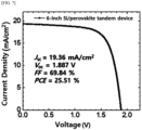
- the perovskite solar cell may be a tandem solar cell.
- it may be a tandem solar cell including an upper cell including a perovskite thin film formed with the coating agent for forming a large-area perovskite thin film described above as a light absorption layer; and a lower cell including Si, Cu(In,Ga)Se 3 , CdTe or a perovskite compound as a light absorption layer.
- the method of forming a perovskite thin film using the coating agent of the present invention does not perform an anti-solvent treatment process, and thus, it is environmentally friendly and has excellent mass productivity.
- the perovskite thin film prepared by using the coating agent and forming method of the present invention has excellent uniformity and thermal stability, and by introducing the same into the light absorption layer of a solar cell, it is possible to manufacture a perovskite solar cell with high energy conversion efficiency.
- the large area means an area of 200 cm 2 or more, and preferably, 250 cm 2 or more.
- the present invention may perform a process including step 1 of preparing a coating agent for forming a perovskite thin film; step 2 of performing a coating process and drying the coating agent on an upper part of a substrate to form a wet-thin film including a perovskite crystallized in an intermediate phase; and step 3 of performing an annealing process on the wet-thin film to form a large-area perovskite thin film including a perovskite compound represented by Chemical Formula 1 below, so as to form and obtain a large-area perovskite thin film.
- [Formula 1] A m A' 1-m B(X n X' 1-n ) 3
- B in Chemical Formula 1 is Pb 2+ , Sn 2+ , Pd 2+ , Cu 2+ , Ge 2+ , Sr 2+ , Cd 2+ , Ca 2+ , Ni 2+ , Mn 2+ , Fe 2+ , Co 2+ , Sn 2+ , Yb 2+ or Eu 2+ , preferably, Pb 2+ , Sn 2+ , Pd 2+ or Cu 2+ , and more preferably, Pb 2+ or Sn 2+ .
- X and X' in Chemical Formula 1 are each independently Cl - , Br - or I - , and preferably, X is I - and X' is Br - .
- m and n in Chemical Formula 1 are rational numbers satisfying 0 ⁇ m ⁇ 1 and 0 ⁇ n ⁇ 1, and are preferably rational numbers satisfying 0.7 ⁇ m ⁇ 0.9 and 0.1 ⁇ n ⁇ 0.3.
- the A m A' 1-m site is formed by mixing a monovalent organic cation with a monovalent inorganic cation to form a monovalent cation.
- A may include amines, ammonium, Group 1 metals, Group 2 metals and/or other cations or cation-like compounds, such as formamidinium (hereinafter, "FA”), methylammonium (hereinafter, “MA”) and FAMA.
- FA formamidinium
- MA methylammonium
- FA-based perovskite which is currently recording the highest efficiency, has low phase stability, and thus, anti-solvent free processes are limited, and uniform large-area thin film coating is difficult.
- the inventors of the present invention attempted to solve the phase stability issue of FA-based perovskite by optimizing the mixing composition. Specifically, the present invention sought to secure phase stability by stabilizing the crystal structure without reducing the thermal stability of the perovskite by introducing a small amount of Group 1 metal cations into the MA Free-based metal halide perovskite.
- the composition (1-m) of the Group 1 metal cation may be controlled to 0.1 or more, and considering the band gap of the tandem device, the composition (1-m) of the metal cation may be controlled to 0.3 or less. Accordingly, the band gap of the perovskite material may be 1.50 eV to 1.80 eV, and preferably, 1.55 eV to 1.72 eV.
- the coating agent for forming a perovskite thin film of the present invention includes a perovskite precursor, a crystallinity enhancer, a Lewis base and a solvent.
- the perovskite precursor includes an organic halide represented by Chemical Formula 2 below, a monovalent metal halide represented by Chemical Formula 3 below, a divalent metal halide represented by Chemical Formula 4 below (a first divalent metal halide) and a divalent metal halide (a second divalent metal halide) represented by Chemical Formula 5 below.
- A is formamidinium (FA), ethylamine (EA), guanidinium (GA) or ethylenediamine (EDA), preferably FA, GA or EDA, and more preferably FA.
- EDA ethylenediamine
- X in Chemical Formula 2 is Br - or I - .
- A' is Cs + , Na + , K + , NH 4 + or Rb + , preferably, Cs + , Na + or K + , and more preferably, Cs + .
- X in Chemical Formula 3 is Br - or I - .
- the crystallinity enhancer may include at least one selected from CH 3 NH 3 Cl (MACl), CH 3 NH 3 Br (MABr) and CH 3 NH 3 I (MAI), preferably, it may include at least one selected from MACl and MABr, and it may preferably include MACl.
- MACl CH 3 NH 3 Cl
- MABr CH 3 NH 3 Br
- MAI CH 3 NH 3 I
- the Lewis base serves to increase the phase stability of the perovskite and prevent the formation of pinholes in the thin film
- a polar aprotic compound may be used, and it may preferably include at least one selected from N,N-dimethyl-propyleneurea (DMPU), hexamethylphosphoramide (HMPA) and N-methyl-2-pyrrolidone (NMP), and preferably, it may include DMPU.
- DMPU N,N-dimethyl-propyleneurea
- HMPA hexamethylphosphoramide
- NMP N-methyl-2-pyrrolidone
- the Lewis base is preferably included in an amount of 40 to 100 mol%, preferably 40 to 90 mol%, and more preferably 50 to 85 mol%, based on 100 mol% of the perovskite precursor in the coating agent.
- the content of the Lewis base is less than 40 mol%, the binding energy of the perovskite crystal intermediate phase in the wet-thin film formed through drying in the thin film formation process is weak, and thus, the perovskite crystal phase may not be formed well, and the uniformity of the thin film may not be good.
- the content of the Lewis base in the coating agent was controlled within the above range.
- the solvent in the perovskite coating agent composition may include at least one selected from dimethylformamide (DMF), gamma-butyrolactone ( ⁇ -butyrolactone), 2-methoxyethanol, dimethyl sulfoxide (DMSO) and N-methyl-2 - pyrrolidinone (NMP), and preferably, it may include at least one selected from DMF, gamma-butyrolactone and 2-methoxyethanol, more preferably, it may include DMF.
- DMF dimethylformamide
- ⁇ -butyrolactone gamma-butyrolactone
- 2-methoxyethanol dimethyl sulfoxide
- NMP N-methyl-2 - pyrrolidinone
- the solvent and the Lewis base in a volume ratio of 1:0.06 to 0.25, preferably the solvent and the Lewis salt in a volume ratio of 1:0.10 to 0.22, and more preferably the solvent and the Lewis salt in a volume ratio of 1:0.10 to 0.18. If the solvent content compared to the Lewis base is too excessive, pinholes may occur in the thin film, and if the solvent content compared to the Lewis base is too small, coating properties may not be secured, and there may be a problem in that surface roughness decrease significantly. Therefore, in the present invention, the solvent content in the coating agent was controlled within the above range.
- step 2 may be performed by blade coating, slot die coating, bar coating, inkjet coating or spray coating, and preferably, it may be performed by blade coating, slot die coating or bar coating.
- the present invention may provide a perovskite solar cell with excellent power conversion efficiency (PCE) by forming a light absorption layer of a solar cell using the coating agent and method for forming a perovskite thin film described above.
- the solar cell of the present invention may be a fin structure-type perovskite solar cell, an inverted-structure perovskite solar cell, a tandem-type perovskite solar cell or a tandem-type silicon/perovskite heterojunction solar cell.
- the light absorption layer of the upper cell may also be formed as a perovskite light absorption layer using the coating agent and method of the present invention.
- the recombination layer is a layer that induces the recombination of electrons and holes generated in the lower cell and the light absorption layer to be described below, and it may be a transparent thin film on which ITO (Induim Tin Oxide), FTO (Fluorine doped Tin Oxide), ATO (Sb 2 O 3 doped Tin Oxide), GTO (Gallium doped Tin Oxide), ZTO (tin doped zinc oxide), ZTO:Ga (gallium doped ZTO), IGZO (Indium gallium zinc oxide, IZO (Indium doped zinc oxide) or AZO (Aluminum doped zinc oxide) is deposited
- the silicon solar cell doped with n- or p-type impurities when using a silicon solar cell doped with n- or p-type impurities as a lower cell, the silicon solar cell doped with n- or p-type impurities may be treated with hydrofluoric acid to remove a SiOx oxide film and then washed with ultrapure water to remove residual hydrofluoric acid, and a recombination layer may be formed on the top of the silicon solar cell from which the oxide film has been removed through a sputtering process.
- the organic hole transport material may include carbazole derivatives, polyarylalkane derivatives, phenylenediamine derivatives, arylamine derivatives, amino-substituted chalcone derivatives, styrylanthracene derivatives, fluorene derivatives, hydrazone derivatives, stilbene derivatives, silazane derivatives., aromatic tertiary amine compounds, styrylamine compounds, aromatic dimethylidine compounds, porphyrin compounds, phthalocyanine compounds, polythiophene derivatives, polypyrrole derivatives, polyparaphenylenevinylene derivatives, pentacene, coumarin 6(coumarin 6, 3-(2-benzothiazolyl)-7-(diethylamino)coumarin), ZnPC (zinc phthalocyanine), CuPC (copper phthalocyanine), TiOPC (titanium oxide phthalocyanine), Spiro-MeOTAD (2,2',7,7'-tetrakis
- methods for forming a hole transport layer may include coating and vacuum deposition methods, and the coating methods may include gravure coating, bar coating, printing, spraying, spin coating, dip and die coating methods.
- the light absorption layer is a large-area thin film layer formed through the coating agent and method of the present invention described above, and it may include a perovskite crystal represented by Chemical Formula 1 above.
- a protective layer may be further included between the hole transport layer and the light absorption layer.
- the protective layer may include a material having a carbazole body with strong hole collecting ability and a phosphonic acid group with strong bonding force with metal oxide, and preferably, it may include SAM materials such as 2-PACz, MeO-2PACz, Br-2PACz, Me-4PACz, MeO-4PACz, 6-PACz and the like.
- a buffer layer may be further included between the electron transport layer and the light absorption layer.
- the buffer layer is a layer formed to prevent interfacial defects and improve transport capacity, and it may include at least one selected from C60, PCBM and PC71BM.
- Methods for forming a buffer layer may include coating and/or vacuum deposition, and the coating methods may include gravure coating, bar coating, printing, spraying, spin coating, blade coating, dip and die coating, and according to one embodiment, a protective layer may be formed on one surface of the light absorption layer through a vacuum deposition method.
- the solar cell may further include a passivation layer between the light absorption layer and the electron transport layer.
- the perovskite precursor was composed of FAI powder (organic halide), CsBr powder (metal halide), PbI 2 powder and PbBr 2 powder at a molar ratio of 1 : 1 : 0.25 : 0.25.
- A is formamidinium (FA)
- A' is Cs +
- B is Pb 2+
- X is I -
- X' is Br -
- m 0.8
- n 0.8.
- a perovskite coating agent and a perovskite thin film using the same were formed on the glass substrate by the same method as in Example 1, except that no Lewis base was used in preparing the coating agent.
- a perovskite coating agent and a perovskite thin film using the same were formed on the glass substrate by the same method as in Example 1, except that as a Lewis base during the preparation of the coating agent, instead of DMPU, 50 mol% of dimethyl sulfoxide (DMSO), which is currently the substance with the highest efficiency in spin coating, was used.
- DMSO dimethyl sulfoxide
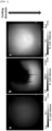
- a is a measurement image of the thin film surface of Comparative Example 1
- b is a measurement image of the thin film surface of Comparative Example 2
- c is a measurement image of the thin film surface of Example 1.
- the thin film surface appears uniform, but overall, the perovskite film was not formed and instead appears uniform.
- Example 2 It was confirmed that there was a problem in that there were areas where perovskite was well formed locally and coated (light-colored areas) and areas where perovskite was not well formed and coated (black areas). On the other hand, in Example 1, it was confirmed that a perovskite thin film with an overall uniform surface was formed.
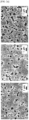
- the large-area perovskite thin film of Comparative Example 2 using DMSO as a Lewis base had a portion (f) where an excellent thin film is formed, but, like Comparative Example 1, there was a problem in that a large amount of pinholes were generated and the thin film was not formed (d,e).
- the large-area perovskite thin film of Example 1 had excellent thin film uniformity overall and did not generate pinholes. This is because the thin film was coated evenly by DMPU (Lewis base), which has a strong bonding energy with the perovskite precursor, and the perovskite crystallinity and bonding strength were improved, and thus, even when large-area coating was performed, it was confirmed that pinholes were not formed, and it was possible to form a uniform thin film.
- DMPU Lewis base
- UV-Vis measurements were performed on the perovskite thin film prepared in Example 1, and the results are shown in FIGS. 3a (absorbance) and FIG. 3b (energy band gap).
- the energy band gap was calculated based on absorbance measurements.
- the energy band gap (E g ) was 1.682 eV, which is a numerical value that satisfies the energy band gap (1.5 eV ⁇ E g ⁇ 1.8 eV) required for the perovskite light absorption layer for the upper cell device of a tandem silicon/perovskite heterojunction solar cell.
- Example 2 used 40 mol% of DMPU, which is a Lewis base
- Example 3 used 60 mol% of DMPU
- Example 4 used 80 mol% of DMPU
- Example 5 used 100 mol% of DMPU during the preparation of the coating agent.
- Comparative Example 3 used 20 mol% of DMPU.
- Perovskite coating agents and perovskite thin films using the same were formed on the glass substrate by the same method as in Example 1, except that as shown in Table 3 below, Examples 6, 7 and 8 used 30, 20 and 15 mol% of CH 3 NH 3 Cl which is a crystallinity enhancer, and Comparative Example 4 used 10 mol% of CH 3 NH 3 Cl which is a crystallinity enhancer to prepare perovskite thin films, respectively.
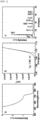
- An opaque device was manufactured by varying the content of MACl, which is a crystallinity enhancer, in a range of 30 to 10 mol%, and IV measurements were performed, and the results are shown in Table 4 and FIG. 5 .
- the average efficiency was generally similar from 15 to 30 mol% in Examples 6 to 8, and the smallest deviation was confirmed to be 18.35% at 25 mol%. Since this plays a role in helping particle growth, which is the role of a generally known crystallinity enhancer, it can be said that the perovskite characteristics are dense and large particles are formed.
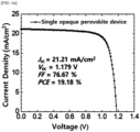
- a single opaque perovskite solar cell device was manufactured using the coating agent for forming a perovskite thin film prepared in Example 1 (Active area: 0.096 cm 2 ).
- the structure of the single opaque device was as follows: NiOx (17 nm), 2PACz (1 nm), a perovskite thin film (550 nm), LiF (1 nm), C60 (13 nm), BCP (8 nm) and a Ag electrode (200 nm) on an organic substrate deposited with ITO (100 nm).
- a single perovskite solar cell device was manufactured in the same manner as Manufacture Example 1, except that the coating agents of Examples 2 to 5, Comparative Example 1 and Comparative Example 3 were used instead of Example 1 to manufacture single opaque perovskite solar cell devices (Active area: 0.096 cm 2 ), so as to perform Manufacture Examples 1-2 to 1-5, Comparative Manufacture Example 1-1 and Comparative Manufacture Example 1-2, respectively (see Table 5 below).
- Comparative Manufacture Example 1-1 and Comparative Manufacture Example 1-2 in which a perovskite coating layer using less than 40 mol% of DMPU, which is a Lewis base, was introduced as a light absorption layer, had photoelectric conversion efficiencies of less than 10.50%. When compared to Manufacture Examples 1-1 to 1-5, it was confirmed that they had relatively very low photoelectric conversion efficiencies.
- Manufacture Examples 1-1 to 1-5 had photoelectric conversion efficiencies of 15.0% or more, preferably 16.0% or more, and Manufacture Example 1-1, which included a light absorption layer formed with the coating agent of Example 1 having a DMPU used amount of 50 mol%, exhibited the best solar cell performance.
Landscapes
- Chemical & Material Sciences (AREA)
- Organic Chemistry (AREA)
- Engineering & Computer Science (AREA)
- Materials Engineering (AREA)
- Life Sciences & Earth Sciences (AREA)
- Wood Science & Technology (AREA)
- Inorganic Chemistry (AREA)
- Physics & Mathematics (AREA)
- Electromagnetism (AREA)
- Photovoltaic Devices (AREA)
- Spectroscopy & Molecular Physics (AREA)
- Electroluminescent Light Sources (AREA)
- Paints Or Removers (AREA)
Applications Claiming Priority (2)
| Application Number | Priority Date | Filing Date | Title |
|---|---|---|---|
| KR1020220066577A KR20230167223A (ko) | 2022-05-31 | 2022-05-31 | 대면적 페로브스카이트 박막 형성용 코팅제 및 이를 이용한 대면적 페로브스카이트 박막 형성 방법 |
| PCT/KR2023/006674 WO2023234601A1 (ko) | 2022-05-31 | 2023-05-17 | 대면적 페로브스카이트 박막 형성용 코팅제 및 이를 이용한 대면적 페로브스카이트 박막 형성 방법 |
Publications (1)
| Publication Number | Publication Date |
|---|---|
| EP4534612A1 true EP4534612A1 (de) | 2025-04-09 |
Family
ID=89025325
Family Applications (1)
| Application Number | Title | Priority Date | Filing Date |
|---|---|---|---|
| EP23816264.8A Pending EP4534612A1 (de) | 2022-05-31 | 2023-05-17 | Beschichtungsmittel zur bildung einer grossflächigen perowskit-dünnschicht und verfahren zur bildung einer perowskit-dünnschicht damit |
Country Status (5)
| Country | Link |
|---|---|
| EP (1) | EP4534612A1 (de) |
| JP (1) | JP2025520038A (de) |
| KR (1) | KR20230167223A (de) |
| CN (1) | CN119213086A (de) |
| WO (1) | WO2023234601A1 (de) |
Families Citing this family (3)
| Publication number | Priority date | Publication date | Assignee | Title |
|---|---|---|---|---|
| DE102024102964A1 (de) * | 2024-02-02 | 2025-08-07 | Hanwha Q Cells Gmbh | Solarmodul |
| CN117881257B (zh) * | 2024-03-11 | 2024-05-28 | 浙江省白马湖实验室有限公司 | 一种高效率碳电极钙钛矿太阳能电池的制备方法 |
| CN118765146B (zh) * | 2024-09-05 | 2024-12-24 | 杭州柯能新能源有限公司 | 一种制作钙钛矿太阳能电池的方法 |
Family Cites Families (10)
| Publication number | Priority date | Publication date | Assignee | Title |
|---|---|---|---|---|
| KR101740654B1 (ko) | 2014-12-08 | 2017-05-26 | 주식회사 엘지화학 | 유무기 하이브리드 페로브스카이트 화합물, 이의 제조방법 및 이를 포함하는 태양전지 |
| KR102164354B1 (ko) * | 2015-06-12 | 2020-10-12 | 옥스퍼드 포토발테익스 리미티드 | 광기전 디바이스 |
| CN106750427B (zh) * | 2016-11-11 | 2020-08-11 | 致晶科技(北京)有限公司 | 一种钙钛矿量子点/聚合物复合荧光膜的制备方法 |
| WO2018152494A1 (en) * | 2017-02-17 | 2018-08-23 | Nutech Ventures | Passivation of defects in perovskite materials for improved solar cell efficiency and stability |
| CN110660911B (zh) * | 2018-06-28 | 2022-09-13 | 华中科技大学鄂州工业技术研究院 | 钙钛矿薄膜及其制备方法和应用 |
| CN109103338B (zh) * | 2018-07-23 | 2020-06-19 | 武汉理工大学 | 一种大面积钙钛矿薄膜及其电池组件的制备方法 |
| KR20200020346A (ko) | 2018-08-17 | 2020-02-26 | 한국화학연구원 | 인라인 연속코팅 페로브스카이트 광활성층 형성방법 및 인라인 연속코팅 장치 |
| GB201908046D0 (en) * | 2019-06-06 | 2019-07-24 | Savvy Science Ltd | Perovskite ink formulations |
| CN110518128B (zh) * | 2019-08-26 | 2023-05-19 | 陕西师范大学 | 一种aci型二维钙钛矿太阳电池及其制备方法 |
| KR102501662B1 (ko) * | 2020-09-08 | 2023-02-21 | 한국전력공사 | 페로브스카이트 전구체 용액, 이를 이용한 페로브스카이트 태양전지, 및 이의 제조방법 |
-
2022
- 2022-05-31 KR KR1020220066577A patent/KR20230167223A/ko active Pending
-
2023
- 2023-05-17 JP JP2024568729A patent/JP2025520038A/ja active Pending
- 2023-05-17 CN CN202380040629.6A patent/CN119213086A/zh active Pending
- 2023-05-17 EP EP23816264.8A patent/EP4534612A1/de active Pending
- 2023-05-17 WO PCT/KR2023/006674 patent/WO2023234601A1/ko not_active Ceased
Also Published As
| Publication number | Publication date |
|---|---|
| KR20230167223A (ko) | 2023-12-08 |
| JP2025520038A (ja) | 2025-07-01 |
| CN119213086A (zh) | 2024-12-27 |
| WO2023234601A1 (ko) | 2023-12-07 |
Similar Documents
| Publication | Publication Date | Title |
|---|---|---|
| KR101949641B1 (ko) | 페로브스카이트막, 이의 제조방법 및 이를 포함하는 태양전지 | |
| EP4534612A1 (de) | Beschichtungsmittel zur bildung einer grossflächigen perowskit-dünnschicht und verfahren zur bildung einer perowskit-dünnschicht damit | |
| CN105830228A (zh) | 无机/有机杂化钙钛矿化合物前体物质 | |
| KR20170026513A (ko) | 무 /유기 하이브리드 페로브스카이트 화합물 막의 제조방법 | |
| WO2017121984A1 (en) | Photoactive polymer-perovskite composite materials | |
| KR20180137431A (ko) | 와이드 밴드갭을 포함하는 페로브스카이트계 태양전지 및 이의 제조방법 | |
| US20250066623A1 (en) | Coating agent for electron transporting layer of inverted perovskite solar cell, and inverted perovskite solar cell containing the same | |
| KR102778499B1 (ko) | 고순도 세슘할라이드 제조방법 및 페로브스카이트 복합재 | |
| KR20230138732A (ko) | 페로브스카이트 박막의 제조방법, 이에 의해 제조된 페로브스카이트 박막을 포함하는 소자 및 이를 이용한 태양전지의 제조방법 | |
| KR102300107B1 (ko) | 페로브스카이트 광전 소자의 제조 방법 및 이를 통하여 제조된 페로브스카이트 광전 소자 | |
| KR102182388B1 (ko) | 와이드 밴드갭을 갖는 페로브스카이트 화합물 막의 후처리 방법 | |
| KR20230052558A (ko) | 페로브스카이트 태양전지용 전자전달층 형성 코팅제, 이를 이용한 페로브스카이트 태양전지용 전자전달층 및 이를 포함하는 페로브스카이트 태양전지의 제조방법 | |
| EP4465790A1 (de) | Perowskit-solarzelle und verfahren zu ihrer herstellung | |
| KR102585825B1 (ko) | 고내구성 페로브스카이트 광전소자 및 이의 제조방법 | |
| KR20240158582A (ko) | 페로브스카이트 박막의 제조방법 및 이를 이용한 페로브스카이트 광흡수층을 형성하기 위한 방법 | |
| EP4563582A1 (de) | Verfahren zur synthese eines delta-phasen-perowskitkristalls und dadurch hergestellter delta-phasen-perowskitkristall | |
| KR102850025B1 (ko) | 탠덤형 실리콘/페로브스카이트 이종접합 태양전지 및 이의 제조방법 | |
| EP4325589A1 (de) | Perowskit-solarzelle und herstellungsverfahren dafür | |
| KR102853063B1 (ko) | 페로브스카이트 광전소자 및 이의 제조 방법 | |
| KR20250121243A (ko) | 대면적 페로브스카이트 박막 형성용 코팅제 및 이를 이용한 대면적 페로브스카이트 박막 형성 방법 | |
| KR102736201B1 (ko) | 페로브스카이트 광전소자 및 이의 제조 방법 | |
| KR102901468B1 (ko) | 델타상 페로브스카이트 결정체 합성방법 및 이 방법으로 제조된 델타상 페로브스카이트 결정체 | |
| KR102766237B1 (ko) | 전자 전달층 용액의 제조 방법, 이를 이용한 전자 전달층의 제조 방법, 이를 통하여 제조된 전자 전달층, 이를 포함하는 페로브스카이트 태양전지의 제조 방법 및 이를 통하여 제조된 페로브스카이트 태양전지 | |
| EP4593564A1 (de) | Elektronenträger für elektronentransportschicht einer perowskitsolarzelle, elektronentransportschichtbeschichtungsmittel damit, elektronentransportschicht und perowskitsolarzelle | |
| KR20250104671A (ko) | 금속 할라이드 전구체의 제조 방법 및 이를 이용하여 제조된 금속 할라이드 전구체, 이를 포함하는 페로브스카이트 광전소자의 제조 방법 및 이를 이용하여 제조된 페로브스카이트 광전소자 |
Legal Events
| Date | Code | Title | Description |
|---|---|---|---|
| STAA | Information on the status of an ep patent application or granted ep patent |
Free format text: STATUS: THE INTERNATIONAL PUBLICATION HAS BEEN MADE |
|
| PUAI | Public reference made under article 153(3) epc to a published international application that has entered the european phase |
Free format text: ORIGINAL CODE: 0009012 |
|
| STAA | Information on the status of an ep patent application or granted ep patent |
Free format text: STATUS: REQUEST FOR EXAMINATION WAS MADE |
|
| 17P | Request for examination filed |
Effective date: 20241120 |
|
| AK | Designated contracting states |
Kind code of ref document: A1 Designated state(s): AL AT BE BG CH CY CZ DE DK EE ES FI FR GB GR HR HU IE IS IT LI LT LU LV MC ME MK MT NL NO PL PT RO RS SE SI SK SM TR |
|
| DAV | Request for validation of the european patent (deleted) | ||
| DAX | Request for extension of the european patent (deleted) |