EP4513487A2 - Dynamische spitzenleistungsverwaltung für mehrchipoperationen - Google Patents
Dynamische spitzenleistungsverwaltung für mehrchipoperationen Download PDFInfo
- Publication number
- EP4513487A2 EP4513487A2 EP25150447.8A EP25150447A EP4513487A2 EP 4513487 A2 EP4513487 A2 EP 4513487A2 EP 25150447 A EP25150447 A EP 25150447A EP 4513487 A2 EP4513487 A2 EP 4513487A2
- Authority
- EP
- European Patent Office
- Prior art keywords
- pull
- ppm
- current
- driver
- memory
- Prior art date
- Legal status (The legal status is an assumption and is not a legal conclusion. Google has not performed a legal analysis and makes no representation as to the accuracy of the status listed.)
- Granted
Links
Images



Classifications
-
- G—PHYSICS
- G11—INFORMATION STORAGE
- G11C—STATIC STORES
- G11C16/00—Erasable programmable read-only memories
- G11C16/02—Erasable programmable read-only memories electrically programmable
- G11C16/06—Auxiliary circuits, e.g. for writing into memory
-
- G—PHYSICS
- G06—COMPUTING OR CALCULATING; COUNTING
- G06F—ELECTRIC DIGITAL DATA PROCESSING
- G06F3/00—Input arrangements for transferring data to be processed into a form capable of being handled by the computer; Output arrangements for transferring data from processing unit to output unit, e.g. interface arrangements
- G06F3/06—Digital input from, or digital output to, record carriers, e.g. RAID, emulated record carriers or networked record carriers
- G06F3/0601—Interfaces specially adapted for storage systems
- G06F3/0602—Interfaces specially adapted for storage systems specifically adapted to achieve a particular effect
- G06F3/0625—Power saving in storage systems
-
- G—PHYSICS
- G06—COMPUTING OR CALCULATING; COUNTING
- G06F—ELECTRIC DIGITAL DATA PROCESSING
- G06F3/00—Input arrangements for transferring data to be processed into a form capable of being handled by the computer; Output arrangements for transferring data from processing unit to output unit, e.g. interface arrangements
- G06F3/06—Digital input from, or digital output to, record carriers, e.g. RAID, emulated record carriers or networked record carriers
- G06F3/0601—Interfaces specially adapted for storage systems
- G06F3/0628—Interfaces specially adapted for storage systems making use of a particular technique
- G06F3/0629—Configuration or reconfiguration of storage systems
-
- G—PHYSICS
- G06—COMPUTING OR CALCULATING; COUNTING
- G06F—ELECTRIC DIGITAL DATA PROCESSING
- G06F3/00—Input arrangements for transferring data to be processed into a form capable of being handled by the computer; Output arrangements for transferring data from processing unit to output unit, e.g. interface arrangements
- G06F3/06—Digital input from, or digital output to, record carriers, e.g. RAID, emulated record carriers or networked record carriers
- G06F3/0601—Interfaces specially adapted for storage systems
- G06F3/0668—Interfaces specially adapted for storage systems adopting a particular infrastructure
- G06F3/0671—In-line storage system
- G06F3/0673—Single storage device
- G06F3/0679—Non-volatile semiconductor memory device, e.g. flash memory, one time programmable memory [OTP]
-
- G—PHYSICS
- G11—INFORMATION STORAGE
- G11C—STATIC STORES
- G11C16/00—Erasable programmable read-only memories
- G11C16/02—Erasable programmable read-only memories electrically programmable
- G11C16/06—Auxiliary circuits, e.g. for writing into memory
- G11C16/30—Power supply circuits
-
- G—PHYSICS
- G11—INFORMATION STORAGE
- G11C—STATIC STORES
- G11C5/00—Details of stores covered by group G11C11/00
- G11C5/06—Arrangements for interconnecting storage elements electrically, e.g. by wiring
- G11C5/063—Voltage and signal distribution in integrated semi-conductor memory access lines, e.g. word-line, bit-line, cross-over resistance, propagation delay
-
- G—PHYSICS
- G11—INFORMATION STORAGE
- G11C—STATIC STORES
- G11C5/00—Details of stores covered by group G11C11/00
- G11C5/14—Power supply arrangements, e.g. power down, chip selection or deselection, layout of wirings or power grids, or multiple supply levels
-
- G—PHYSICS
- G11—INFORMATION STORAGE
- G11C—STATIC STORES
- G11C5/00—Details of stores covered by group G11C11/00
- G11C5/14—Power supply arrangements, e.g. power down, chip selection or deselection, layout of wirings or power grids, or multiple supply levels
- G11C5/147—Voltage reference generators, voltage or current regulators; Internally lowered supply levels; Compensation for voltage drops
-
- H—ELECTRICITY
- H10—SEMICONDUCTOR DEVICES; ELECTRIC SOLID-STATE DEVICES NOT OTHERWISE PROVIDED FOR
- H10D—INORGANIC ELECTRIC SEMICONDUCTOR DEVICES
- H10D84/00—Integrated devices formed in or on semiconductor substrates that comprise only semiconducting layers, e.g. on Si wafers or on GaAs-on-Si wafers
- H10D84/80—Integrated devices formed in or on semiconductor substrates that comprise only semiconducting layers, e.g. on Si wafers or on GaAs-on-Si wafers characterised by the integration of at least one component covered by groups H10D12/00 or H10D30/00, e.g. integration of IGFETs
- H10D84/811—Combinations of field-effect devices and one or more diodes, capacitors or resistors
-
- G—PHYSICS
- G11—INFORMATION STORAGE
- G11C—STATIC STORES
- G11C16/00—Erasable programmable read-only memories
- G11C16/02—Erasable programmable read-only memories electrically programmable
- G11C16/04—Erasable programmable read-only memories electrically programmable using variable threshold transistors, e.g. FAMOS
- G11C16/0483—Erasable programmable read-only memories electrically programmable using variable threshold transistors, e.g. FAMOS comprising cells having several storage transistors connected in series
Definitions
- the present disclosure generally relates to the field of semiconductor technology, and more particularly, to circuit designs and methods for peak power management in a storage system.
- a NAND storage system is widely used as the primary non-volatile storage device due to its high storage density and relatively low access latency.
- performance of a high density storage system for example, a three-dimensional (3D) NAND storage system, is often restricted by the maximum amount of power (or peak current) that it can use.
- peak power operations operations consuming high power (i.e., peak power operations) that are carried out by various memory dies of the NAND storage system can be staggered by a system controller. Only a limited number of peak power operations can be performed simultaneously. This approach can also result in increased system loading with unnecessary over-management. Communications between different memory dies can be established to coordinate the peak power operations.
- An aspect of the present disclosure is to provide effective peak power management for a memory storage system.
- the PPM system includes a PPM circuit on each of the multiple memory dies.
- Each PPM circuit includes a pull-up driver electrically connected to a power source and a PPM resistor; a pull-down driver electrically connected to the PPM resistor; and a PPM contact pad connected to the PPM resistor.
- PPM contact pads of the multiple memory dies are electrically connected with each other.
- the PPM system is configured to manage a peak power operation based on an electric potential of the PPM contact pads.
- the PPM system further includes a comparator with a first input terminal electrically connected to the PPM contact pads of the multiple memory dies and a second input terminal electrically connected to a reference voltage.
- an output terminal of the comparator is connected to an inverter.
- an RC filter is electrically connected to the PPM contact pads of the multiple memory dies and the first input terminal of the comparator.
- the reference voltage is based on a maximum total current allowed on the memory chip.
- the electric potential of the PPM contact pads is adjusted by a pull-down current flowing through the pull-down driver in the PPM circuit.
- the pull-down current includes a high current level, the high current level corresponding to a peak current of the peak power operation.
- the pull-up driver includes a p-channel metal oxide semiconductor field effect transistor (MOSFET).
- MOSFET metal oxide semiconductor field effect transistor
- the pull-down driver includes an n-channel metal oxide semiconductor field effect transistor (MOSFET).
- MOSFET metal oxide semiconductor field effect transistor
- the PPM contact pad, the PPM resistor and the pull-down driver are electrically connected.
- the PPM contact pad, the PPM resistor and the pull-up driver are electrically connected.
- the PPM contact pads are electrically connected through die-to-die connections, each die-to-die connection including a metal interconnect.
- the PPM contact pads are electrically connected through flip-chip bonding, die-to-die bonding, or wire-bonding.
- PPM peak power management
- the PPM method includes the following steps: switching on a pull-down driver of the PPM circuit on a selected memory die of the memory chip; verifying a PPM enablement signal regulated by a pull-down current flowing through the pull-down driver; and performing a peak power operation on the selected memory die when the PPM enablement signal indicates that a total current of the memory chip is less than a maximum total current allowed for the memory chip.
- the method further includes, after performing the peak power operation, setting the pull-down current flowing through the pull-down driver on the selected memory die to a low current level, wherein the low current level correspond to a base current on the selected memory die.
- the method further includes switching off the pull-down driver on the selected memory die if the PPM enablement signal indicates that the total current of the memory chip is more than the maximum total current allowed for the memory chip.
- the method also includes, after switching off the pull-down driver, waiting for a delay time period.
- the method further includes, prior to verifying the PPM enablement signal, generating the PPM enablement signal by comparing a reference voltage with an electric potential of the PPM contact pads.
- the reference voltage is selected according to the maximum total current allowed for the memory chip.
- the method also includes regulating the electric potential of the PPM contact pads through the pull-down current of the pull-down driver, wherein the total current of the memory chip corresponds to a sum of the pull-down current flowing through each pull-down driver on the memory chip.
- the PPM enablement signal is set to 0 if the electric potential of the PPM contact pads is higher than the reference voltage; and the PPM enablement signal is set to 1 if the electric potential of the PPM contact pads is lower than the reference voltage.
- references in the specification to "one embodiment,” “an embodiment,” “an example embodiment,” “some embodiments,” etc. indicate that the embodiment described can include a particular feature, structure, or characteristic, but every embodiment can not necessarily include the particular feature, structure, or characteristic. Moreover, such phrases do not necessarily refer to the same embodiment. Further, when a particular feature, structure or characteristic is described in connection with an embodiment, it would be within the knowledge of a person skilled in the pertinent art to affect such feature, structure or characteristic in connection with other embodiments whether or not explicitly described.
- terminology can be understood at least in part from usage in context.
- the term "one or more” as used herein, depending at least in part upon context can be used to describe any feature, structure, or characteristic in a singular sense or can be used to describe combinations of features, structures or characteristics in a plural sense.
- terms, such as “a,” “an,” or “the,” again, can be understood to convey a singular usage or to convey a plural usage, depending at least in part upon context.
- the term “based on” can be understood as not necessarily intended to convey an exclusive set of factors and may, instead, allow for existence of additional factors not necessarily expressly described, again, depending at least in part on context.
- the term "nominal/nominally” refers to a desired, or target, value of a characteristic or parameter for a component or a process step, set during the design phase of a product or a process, together with a range of values above and/or below the desired value.
- the range of values can be due to slight variations in manufacturing processes or tolerances.
- the term “about” indicates the value of a given quantity that can vary based on a particular technology node associated with the subject semiconductor device. Based on the particular technology node, the term “about” can indicate a value of a given quantity that varies within, for example, 10-30% of the value (e.g., ⁇ 10%, ⁇ 20%, or ⁇ 30% of the value).
- the host computer 15 sends data to be stored at the NAND storage system or SSD 10 or retrieves data by reading the SSD 10.
- the host controller 20 can handle I/O requests received from the host computer 15, ensure data integrity and efficient storage, and manage the memory chip 25.
- the memory channels 30 can provide data and control communication between the host controller 20 and each memory chip 25 via a data bus.
- the host controller 20 can select one of the memory chip 25 according to a chip enable signal.
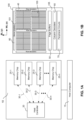
- the exemplary NAND flash memory 100 includes four memory planes 101 and each memory plane 101 includes six memory blocks 103.
- Each memory block 103 can include a plurality of memory cells, where each memory cell can be addressed through interconnections such as bit lines and word lines.
- the bit lines and word lines can be laid out perpendicularly (e.g., in rows and columns, respectively), forming an array of metal lines.
- the direction of bit lines and word lines are labeled as "BL" and "WL” in FIG. 1B .
- the memory block 103 is also referred to as the "memory array" or "array.”
- the memory array is the core area on a memory die, performing storage functions.
- the SSD 10 and the NAND flash memory 100 in FIGs. 1A and 1B are shown as examples.
- the SSD 10 and the NAND flash memory 100 can have other layout and can include additional components.
- the NAND flash memory 100 can also have high-voltage charge pumps, I/O circuits, etc.
- the SSD 10 can also include firmware, data scrambler, etc.
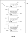
- FIG. 2 illustrates a peak power management system 200 of the memory chip 25, according to some embodiments of the present disclosure.
- the peak power management (PPM) system 200 can be implemented in each memory chip 25 of the NAND storage system 10 in FIG. 1A , where each memory chip 25 can include a plurality of memory dies 100-1, 100-2, 100-3, ..., 100- n , and each memory die can be similar to the NAND flash memory 100 discussed previously in reference with FIG. 1B .
- each NAND flash memory 100 can include a peak power management (PPM) circuit 202 where each PPM circuit 202 can include a PPM contact pad 204 (also referred to as PPM pin).
- PPM peak power management
- the PPM circuits 202-1, 202-2, 202-3, ..., 202- n on different NAND flash memories 100-1, 100-2, 100-3, ..., 100- n of the memory chip 25 can communicate with each other through the PPM pins 204-1, 204-2, 204-3, ..., 204- n .
- the PPM pins between different NAND flash memories 100 can be electrically connected with each other through a plurality of die-to-die connections 205.
- the PPM pin 204-2 on the NAND flash memory 100-2 can be electrically connected with the PPM pin 204-1 on the NAND flash memory 100-1 through the die-to-die connection 205-1 and can be electrically connected with the PPM pin 204-3 on the NAND flash memory 100-3 through the die-to-die connection 205-2.
- the die-to-die connections 205 can be a metal wire formed through wire-bonding.
- the die-to-die connections 205 can be metal wires or any suitable metal or conductive material formed through flip-chip bonding or any suitable die-to-die bonding.
- the die-to-die connections 205 can be formed by through-silicon VIAs (e.g, through-array structures).
- NAND flash memories 100-1, 100-2, 100-3, ..., 100-n can be established in the memory chip 25.
- the NAND storage system 10 can send operation commands to any number of memory dies at any time while the PPM circuits 202 can control the system's power consumption by selecting one or more memory dies.
- FIG. 3 illustrates an exemplary PPM circuit 202 on the NAND flash memory 100, according to some embodiments of the present disclosure.
- the PPM circuit 202 can include a pull-up driver 314, where one terminal of the pull-up driver 314 is connected to a power source 312 with a voltage V dd .
- the pull-up driver 314 can be a metal-oxide-semiconductor-field-effect-transistor (MOSFET).
- MOSFET metal-oxide-semiconductor-field-effect-transistor
- the pull-up driver 314 can be a p-channel MOSFET (i.e., pFET), where a source terminal of the pFET 314 can be connected to the power source 312 and a drain terminal of the pFET 314 can be connected to a PPM resistor 318 with a resistance R ppm .
- pFET p-channel MOSFET
- the PPM circuit 202 also includes a pull-down driver 336.
- the pull-down driver 336 can be a MOSFET.
- the pull-down driver 336 can be an n-channel MOSFET (i.e., nFET). A source terminal of the nFET 336 can be grounded, and a drain terminal of the nFET 336 can be connected to the PPM resistor 318.
- the PPM resistor 318 and the drain terminal of the nFET 336 are also electrically connected to the PPM contact pad 204 at a node 322.
- Some or all the PPM contact pads e.g., the PPM pins 204) can be electrically connected through the die-to-die connections 205 (see FIG. 2 ).
- the PPM contact pads 204 of the memory chip 25 can be held to an electrical potential V ppm at the node 322.
- the PPM circuit 202 can also include a comparator 328, with a first input terminal 324 at a reference voltage V ref and a second input terminal 326 connected to the node 322.
- the comparator 328 can be an operational amplifier used for comparing an input voltage V in at the second input terminal 326 with the reference voltage V ref at the first input terminal 324, where an output voltage V out at an output terminal 330 can indicate whether the input voltage V in is above or below the reference voltage V ref .
- the output voltage V out can be a positive voltage when the input voltage V in is larger than the reference voltage V ref .
- the output voltage V out can be a negative voltage when the input voltage V in is smaller than the reference voltage V ref .
- the PPM circuit 202 can further include an inverter 332 with an input terminal connected to the output terminal 330 of the comparator 328.
- RC filter 344 there can be an optional RC filter 344 connected between the node 322 and the second input terminal 326 of the comparator 328.
- the RC filter 344 can be used to filter out unwanted signals within a certain frequency range.
- the PPM pins on the same memory chip are electrically connected, i.e., all the PPM pins of the same PPM group have the same electrical potential V ppm . Therefore, each memory chip only needs one comparator 328 electrically connected at the node 322 to the PPM contact pads 204. And the PPM enablement signal enPPM indicates the electrical potential V ppm for multiple the memory dies on the memory chip.
- a first control signal 340 can be sent to a gate terminal 316 of the pFET 314 to switch the pFET 314 on or off.
- the pFET 314 can be switched on, and a conductive path can be formed from the power source 312 to the PPM resistor 318.
- the current flowing through the pull-up driver 314 and the PPM resistor 318 is also referred to as a pull-up current I pull_up . If the first control signal 340 has a voltage higher than the threshold voltage of the pFET 314, the pFET 314 can be switched off.
- the nFET 336 can be switched on or off. For example, if the second control signal 342 has a voltage higher than a threshold voltage of the nFET 336, the nFET 336 can be switched on, and a conductive path can be formed from the node 322 to the ground. If the second control signal 342 has a voltage less than the threshold voltage of the nFET 336, the nFET 336 can be switched off.
- the pull-down driver 336 can be operated as a current controller.
- the pull-down driver 336 when the pull-down driver 336 is switched on, the magnitude of the current flowing through the pull-down driver 336 from the node 322 to the ground (also referred to as pull-down current I pull_dn ) depends on the second control signal 342.
- the pull-down driver 336 is an nFET, as shown in FIG. 3 , the pull-down current I pull_dn can be determined by the voltage level of the second control signal 342 and the trans-conductance of the nFET 336.
- a current profile I cc of a memory die (e.g., the NAND flash memory 100-1) can correspond to the voltage level of the second control signal 342, and thereby correspond to the pull-down current I pull_dn . Therefore, the pull-down current I pull_dn can function as a current mirror of the current profile I cc of the memory die.
- the pull-down current I pull_dn can be proportional to a current level of the current profile I cc .
- the pull-down current I pull_dn can be scaled down proportionally from the current profile I cc .
- the pull-down current I pull_dn of the PPM circuit 202 can be 200 ⁇ A. Therefore, memory operations and corresponding current can be regulated for each memory die through the pull-down current I pull_dn .
- peak power operations throughout the entire memory chip can be coordinated between different memory dies.
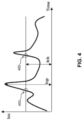
- FIG. 4 shows an exemplary current profile I cc of a memory die (e.g., the NAND flash memory 100 in FIG. 2 ), according to some embodiments of the present disclosure.
- the current profile I cc can include two defined current levels, a peak current I cp and a base current I cb .
- the peak current I cp corresponds to a current level when the memory die is performing a peak power operation.
- the base current I cb corresponds to an average current level when the memory die is performing regular operations.
- the current profile I cc of a memory die rises to the base current I cb , the memory die arrives at a break point 450. Due to an increasing trend of current, a PPM scheme can be implemented to control total current consumed by the memory chip among the multiple memory dies.
- the pull-down current I pull_dn can also be defined using two current levels, i.e., a high current level I H (or a first current level) and a low current level I L (or a second current level).
- the high current level I H of the pull-down current I pull_dn corresponds to the peak current I cp of a specific memory die.
- the low current level I L of the pull-down current I pull_dn corresponds to the base current I cb of the specific memory die.
- only one pull-up driver 314 is switched on (i.e., enabled) in a memory chip and the other pull-up drivers 314 on different memory dies of the same memory chip can be switched off.
- current only flows from the power source 312 through one PPM resistor 318 on each memory chip.
- the PPM circuits 202 on the same memory chip share a shared pull-up driver 314 and a shared PPM resistor 318.
- the pull-down driver 336 can be switched on or off depending on the status of the memory die, and can be independently controlled according to the PPM management scheme discussed below.
- the NAND flash memory 100-1 (in FIG. 2 ) can perform a peak power operation using the peak current I cp when the pull-down driver 336 of the PPM circuit 202-1 is switched on, where a conductive path can be formed through the pull-down driver 336 to the ground with the pull-down current I pull_dn at the high current level I H .
- the NAND flash memories 100-1 is prohibited from performing any peak power operation when the pull-down driver 336 of the PPM circuit 202-1 is switched off, where no current can flow through the pull-down driver 336 on the NAND flash memory 100-1.
- the electric potential V ppm of the node 322 depends on the number of pull-down drivers 336 that are switched on and depends on current levels of the pull-down current I pull_dn going through the pull-down drivers 336.
- a peak power operation can be performed on a memory die when the pull-down driver 336 is switched on and the pull-down current I pull_dn is at the high current level I H .
- a total current I total used by the memory chip can be controlled and the number of peak power operations performed in a memory chip having multiple memory dies can thereby be regulated.
- FIG. 5 shows an equivalent PPM circuit 500 on a memory chip of multiple memory dies, according to some embodiments of the present disclosure.
- the equivalent PPM circuit 500 represents the PPM circuits 202 across different memory dies, as shown in FIGs. 2 and 3 . Since only the pull-up driver 314 and the pull-down drivers 336 that are switched on can form conductive paths, Figure 5 omits those pull-up drivers 314 and pull-down drivers 336 that are switched off.
- the node 322 is electrically connected to the PPM pin 204 on the memory die (see FIG. 3 ), and all the PPM pins 204 in the same memory chip are electrically connected between different memory dies (see FIG. 2 ). Therefore, the node 322 can be held at the same electrical potential V ppm between different memory dies on the same memory chip, and is illustrated as one intersection point to the PPM resistor 318 in FIG. 5 .
- only one pull-up driver 314 can be switched on for peak power management across multiple memory dies on the same memory chip.
- the pull-down driver 336 can be switched on in the PPM circuit corresponding to the memory die performing the peak power operation, i.e., using the peak current I cp .
- pull-down drivers 336 there can be m number of pull-down drivers 336 that are switched on in a memory chip, where m can be any whole number.
- the pull-down drivers 336 are from the PPM circuits 202 of the memory dies, e.g., NAND flash memory 100-1, 100-2, ..., 100- m in FIG. 2 .
- the pull-down drivers 336 are connected in parallel with each other.
- the pull-down current I pull_dn can be set at either the high level current I H or the low level current I L , depending on the operations performed on the specific memory die.
- the pull-up current I pull_up can be a total current of the PPM circuits on the same memory chip.
- the pull-up current I pull_up can correspond to a total current I total of the memory chip.
- the pull-up current I pull_up (in Equation 1) and the total current I total of the memory chip can follow the same scaling ratio as the pull-down current I pull_dn (e.g., the high and low current level I H and I L ) of the PPM circuit 202 and the current profile I cc (e.g., the peak and base current I cp and I cb ) of the memory chip. For example, if the total current I total of a memory chip is 1000 mA, the pull-up current I pull_up of the PPM circuits 202 can be 1000 ⁇ A.
- the maximum pull-up current I pull_up_max of the PPM circuit 202 (in FIG.
- the maximum total current I total_max of the memory chip 25 follows the same scaling ratio as the pull-down current I pull_dn (e.g., the high and low current level I H and I L ) of the PPM circuit 202 and the current profile I cc (e.g., the peak and base current I cp and I cb ) of the memory chip.
- the maximum total current I total_max allowed on a memory chip is 1000 mA
- the maximum pull-up current I pull_up_max of the PPM circuit 202 can be 1000 ⁇ A.
- the pull-up current I pull_up when the pull-up current I pull_up is less than the maximum pull-up current I pull_up_max , based on the Equations (2) and (3), the electric potential V ppm is higher than the reference voltage V ref .
- the pull-up current I pull_up when the pull-up current I pull_up is more than the maximum pull-up current I pull_up_max , the electric potential V ppm is lower than the reference voltage V ref .
- the pull-down current I pull_dn on each memory die can be adjusted.
- the pull-up current I pull_up can be regulated accordingly.
- the PPM enablement signal enPPM can be set at 0 or 1.
- the reference voltage V ref can be programmed to correspond to the maximum total current I total_max allowed on the memory chip.
- the PPM enablement signal enPPM can be used to indicate whether there are still current or power budget to run additional peak power operations.
- the memory chip 25 can provide the peak current I cp to at least one of the memory dies, i.e., having enough power (or current) to provide at least one additional memory die to perform peak power operation.
- the PPM enablement signal enPPM 1
- the maximum pull-up current I pull_up_max of the PPM circuit 202 has been reached, indicating that the maximum total current I total_max of the memory chip 25 has been reached.
- the memory chip 25 has reached its power (or current) limit and cannot provide additional peak current I cp to any of the memory dies to perform any additional peak power operation.
- FIG. 6 illustrates a peak power check routine 600 associated with the peak power management system 200 in FIG. 2 and the PPM circuit 202 in FIG. 3 , according to some embodiments of the present disclosure.
- the PPM scheme described with reference with FIGs.2-5 is used to determine the reference voltage V ref and generate the PPM enablement signal enPPM to indicate whether the NAND storage system 10 is operating at a current level below the maximum total current I total_max allowed on the memory chip 25.
- the peak power check (PPC) routine 600 are not exhaustive and that other operation steps can be performed as well before, after, or between any of the illustrated operation steps. In some embodiments, some operation steps of the PPC routine 600 can be omitted or other operation steps can be included, which are not described here for simplicity. In some embodiments, operation steps of the PPC routine 600 can be performed in a different order and/or vary.
- the PPC routine 600 provides an exemplary method of managing peak power usage for a memory chip with one or more memory dies, where each memory die includes at least one PPM circuit.
- the example below is shown for a memory chip, e.g., the memory chip 25 in FIG. 2 , where each memory die includes the PPM circuit 202 for checking and regulating peak power operations performed by the memory dies.
- the method can be extended to a memory chip where each memory die includes two or more PPM circuits.
- the PPC routine 600 can be implemented before a memory die starts to perform a peak power operation such that the total power (or current) consumed by a memory chip can be regulated and controlled to below a predetermined value, e.g., the maximum total current I total_max .
- the PPC routine 600 starts at operation step S605, when a NAND storage system (e.g., the NAND storage system 10 in FIG. 1 ) determines that one of the memory dies (e.g., the NAND flash memory 100-1) on the memory chip 25 arrives at a break point (e.g., the break point 450 shown in FIG. 4 ). Compared with the current level prior to the break point 450, the increased current consumption on the memory die indicates that the memory die may perform a peak power operation subsequently.
- a NAND storage system e.g., the NAND storage system 10 in FIG. 1
- the memory dies e.g., the NAND flash memory 100-1
- the PPM circuit 202-1 on the NAND flash memory 100-1 can be at a reset state.
- the pull-down driver 336-1 is switched off.
- one of the pull-up drivers 314 of the PPM circuits 202 can be switched on as a shared pull-up driver among the multiple memory dies on the memory chip.
- the pull-down driver 336-1 on the NAND flash memory 100-1 can be switched on.
- the pull-down current I pull_dn_1 flowing through the pull-down driver 336-1 on the NAND flash memory 100-1 can be set to the high current level I H , which corresponds to the peak current I cp needed to perform the peak power operation on the NAND flash memory 100-1.
- the NAND flash memory 100-1 performs the peak power operation running at the peak current I cp .
- the NAND flash memory 100-1 can also perform any operation running at a current level less than the peak current I cp .
- the PPC routine 600 continues to operation step S630, where the pull-down driver 336-1 on the NAND flash memory 100-1 can be switched off.
- the PPC routine 600 is paused and waits for a delay time period t dl .
- the delay time period t dl is random.
- the delay time period t dl can be any suitable time period in a range between 0.1 ⁇ s to 100 ⁇ s.
- the delay time period t dl can be different for each memory die.
- the delay time period t dl is introduced in event that multiple memory dies enter the PPC routine 600 at the same time and multiple pull-down drivers are switched on and set at the high current level I H at the same time. If there is no current/power budget available to run the peak power operations for these memory dies at the same time, the PPM enablement signal enPPM indicates to the multiple memory dies at operation step S620. Then the corresponding pull-down drivers can be switched off on the multiple memory dies simultaneously at operations step S630.
- the multiple memory dies can return to operation step S620 one at a time, i.e., the requests for peak power operations from multiple memory dies can be de-synchronized. As such, the multiple memory dies can perform the peak power operation sequentially without exceeding the maximum total current I total_max allowed on the memory chip.
- the pull-down current I pull_dn_1 flowing through the pull-down driver 336-1 can be set to the low current level I L .
- the NAND flash memory 100-1 can continue operations with current less than the peak current I cp .
- the PPC routine 600 can return back via loop L2 to operation step S605, for example, when another break point is detected after the completion of the present peak power operation.
- the pull-down driver 336-1 of the PPM circuit 202-1 on the NAND flash memory 100-1 can be disabled (i.e., switched off), for example, when the current level of the NAND flash memory 100-1 falls below the base current I cb .
- the PPC routine 600 is finished and can be restarted again if the NAND storage system 10 determines that one of the memory dies on the memory chip enters one of the break points.
- the current/power budget can be temporary reserved for this specific memory die. Any other memory die on the same memory chip that runs the PPC routine 600 can be queued in the loop of operation steps S620, S630 and S635 unless the total current I total is less than the maximum total current I total_max or until the current/power budget is available on the memory chip, which can be verified at the operation step S620.
- the electric potential V ppm of the PPM contact pads 204 across multiple memory dies on the memory chip can be regulated because the PPM contact pads 204 on different memory dies can be electrically connected through the die-to-die connections 205 and can be held at the same electric potential V ppm .
- the PPM circuit and PPM scheme are not limited to the examples shown in FIGs. 3-6 . Variations of the PPM circuit 202 and the PPC routine 600 can provide similar peak power manage for a memory chip with multiple memory dies.
- FIG. 7 illustrates another exemplary PPM circuit 202' on the NAND flash memory 100, according to some embodiments of the present disclosure.
- the PPM circuit 202' is similar to the PPM circuit 202.
- the main difference is that the PPM resistor 318 can be connected between the node 322 and the pull-down driver 336.
- the pull-up driver 314 can be regulated according to the current profile I cc on the memory die.
- the pull-up current I pull_up of the PPM circuit 202' can be defined with two current levels, e.g., the high current level I H and the low current level I L , corresponding the peak current I cp and the base current I cb of the memory die.
- I pull_dn_max is a maximum pull-down current flowing through the pull-down driver 336, corresponding to the maximum total current I total_max allowed on a memory chip.
- PPC routing 600 can be modified by switching the pull-down driver / pull-down current to pull-up driver / pull-up current.
- the devices and configurations used for the exemplary PPM circuit 202 in FIG. 3 and the PPM circuit 202' in FIG. 7 are only for illustration purpose and for simplicity to demonstrate the functionality of the PPM circuit and PPM scheme.
- the pull-down driver 336 in FIG. 3 can be replaced by a suitable current source to set the current levels of the pull-down current I pull_dn .
- Dynamic peak power management of a memory chip discussed above can also be implemented to closely follow the current profile I cc of a memory die.
- the pull-down current I pull_dn can be adjusted to be proportional to the peak current I i of each phase P;.
- the break point 450 can be inserted at the beginning of phase P 1 and each phase P i if the peak current I i is larger than the peak current I i - 1 of the previous phase P i-1 .
- break points 450 can be inserted at the beginning of phase P 1 , P 2 and P 4 in FIG. 8 .
- operation step S605 can be started.
- the pull-down driver 336 on the memory die can be enabled at operation step S610, and the pull-down current I pull_dn flowing through the pull-down driver 336 can be set at a current level reflecting the peak current I 2 in phase P 2 .
- the pull-down current I pull_dn can be adjusted to a lower level to be proportional to the next peak current of the memory die. For example, when the peak power operation is completed for phase P 2 , the pull-down current I pull_dn of the memory die can be adjusted to be proportional to the peak current I 3 and continues to execute the operations in phase P 3 .
- phase P 4 At the beginning of phase P 4 , another break point 450 is detected.
- the PPC routine 600 returns back to operation step S605 and the PPM enablement signal enPPM is checked again at operation step S620.
- the present disclosure provides a peak power management (PPM) system for a memory chip with multiple memory dies.
- the PPM system includes a PPM circuit on each of the multiple memory dies.
- Each PPM circuit includes a pull-up driver electrically connected to a power source and a PPM resistor; a pull-down driver electrically connected to the PPM resistor; and a PPM contact pad connected to the PPM resistor.
- PPM contact pads of the multiple memory dies are electrically connected with each other.
- the PPM system is configured to manage a peak power operation based on an electric potential of the PPM contact pads.
- the present disclosure also provides a method of peak power management (PPM) for a memory chip with multiple memory dies, wherein each of the multiple memory dies includes a PPM circuit having a PPM contact pad. PPM contact pads of the multiple memory dies are electrically connected.
- the PPM method includes the following steps: switching on a pull-down driver of the PPM circuit on a selected memory die of the memory chip; verifying a PPM enablement signal regulated by a pull-down current flowing through the pull-down driver; and performing a peak power operation on the selected memory die when the PPM enablement signal indicates that a total current of the memory chip is less than a maximum total current allowed for the memory chip.
Landscapes
- Engineering & Computer Science (AREA)
- Power Engineering (AREA)
- Theoretical Computer Science (AREA)
- Physics & Mathematics (AREA)
- General Engineering & Computer Science (AREA)
- General Physics & Mathematics (AREA)
- Human Computer Interaction (AREA)
- Read Only Memory (AREA)
- Microelectronics & Electronic Packaging (AREA)
- Memory System (AREA)
- Dram (AREA)
- Semiconductor Memories (AREA)
- Techniques For Improving Reliability Of Storages (AREA)
- For Increasing The Reliability Of Semiconductor Memories (AREA)
Priority Applications (2)
| Application Number | Priority Date | Filing Date | Title |
|---|---|---|---|
| EP25150447.8A EP4513487B1 (de) | 2020-11-26 | 2020-11-26 | Dynamische spitzenleistungsverwaltung für mehrchipoperationen |
| EP26155704.5A EP4734113A2 (de) | 2020-11-26 | 2020-11-26 | Dynamische spitzenleistungsverwaltung für mehrchipoperationen |
Applications Claiming Priority (3)
| Application Number | Priority Date | Filing Date | Title |
|---|---|---|---|
| EP25150447.8A EP4513487B1 (de) | 2020-11-26 | 2020-11-26 | Dynamische spitzenleistungsverwaltung für mehrchipoperationen |
| PCT/CN2020/131692 WO2022109901A1 (en) | 2020-11-26 | 2020-11-26 | Dynamic peak power management for multi-die operations |
| EP20962792.6A EP4147238B1 (de) | 2020-11-26 | 2020-11-26 | Dynamische spitzenleistungsverwaltung für mehrchipoperationen |
Related Parent Applications (1)
| Application Number | Title | Priority Date | Filing Date |
|---|---|---|---|
| EP20962792.6A Division EP4147238B1 (de) | 2020-11-26 | 2020-11-26 | Dynamische spitzenleistungsverwaltung für mehrchipoperationen |
Related Child Applications (1)
| Application Number | Title | Priority Date | Filing Date |
|---|---|---|---|
| EP26155704.5A Division EP4734113A2 (de) | 2020-11-26 | 2020-11-26 | Dynamische spitzenleistungsverwaltung für mehrchipoperationen |
Publications (3)
| Publication Number | Publication Date |
|---|---|
| EP4513487A2 true EP4513487A2 (de) | 2025-02-26 |
| EP4513487A3 EP4513487A3 (de) | 2025-05-21 |
| EP4513487B1 EP4513487B1 (de) | 2026-02-18 |
Family
ID=75145395
Family Applications (3)
| Application Number | Title | Priority Date | Filing Date |
|---|---|---|---|
| EP20962792.6A Active EP4147238B1 (de) | 2020-11-26 | 2020-11-26 | Dynamische spitzenleistungsverwaltung für mehrchipoperationen |
| EP26155704.5A Pending EP4734113A2 (de) | 2020-11-26 | 2020-11-26 | Dynamische spitzenleistungsverwaltung für mehrchipoperationen |
| EP25150447.8A Active EP4513487B1 (de) | 2020-11-26 | 2020-11-26 | Dynamische spitzenleistungsverwaltung für mehrchipoperationen |
Family Applications Before (2)
| Application Number | Title | Priority Date | Filing Date |
|---|---|---|---|
| EP20962792.6A Active EP4147238B1 (de) | 2020-11-26 | 2020-11-26 | Dynamische spitzenleistungsverwaltung für mehrchipoperationen |
| EP26155704.5A Pending EP4734113A2 (de) | 2020-11-26 | 2020-11-26 | Dynamische spitzenleistungsverwaltung für mehrchipoperationen |
Country Status (7)
| Country | Link |
|---|---|
| US (4) | US11467741B2 (de) |
| EP (3) | EP4147238B1 (de) |
| JP (2) | JP7467692B2 (de) |
| KR (2) | KR102901824B1 (de) |
| CN (2) | CN117577152A (de) |
| TW (2) | TWI835209B (de) |
| WO (1) | WO2022109901A1 (de) |
Families Citing this family (10)
| Publication number | Priority date | Publication date | Assignee | Title |
|---|---|---|---|---|
| US12400717B2 (en) * | 2020-11-11 | 2025-08-26 | Yangtze Memory Technologies Co., Ltd. | Analog peak power management for multi-die operations |
| WO2022099493A1 (en) | 2020-11-11 | 2022-05-19 | Yangtze Memory Technologies Co., Ltd. | Analog peak power management for multi-die operations |
| CN117577152A (zh) | 2020-11-26 | 2024-02-20 | 长江存储科技有限责任公司 | 用于多管芯操作的动态峰值功率管理 |
| US11990197B2 (en) * | 2020-12-21 | 2024-05-21 | Micron Technology, Inc. | Peak power management connectivity check in a memory device |
| US12333145B2 (en) * | 2021-12-21 | 2025-06-17 | Micron Technology, Inc. | Peak power management in a memory device during suspend status |
| US12436692B2 (en) | 2022-08-19 | 2025-10-07 | Micron Technology, Inc. | Peak power management data burst communication |
| US12455817B2 (en) | 2022-10-27 | 2025-10-28 | Micron Technology, Inc. | Dual data channel peak power management |
| US12455608B2 (en) * | 2022-11-18 | 2025-10-28 | Micron Technology, Inc. | Peak power management extensions to application-specific integrated circuits |
| US12585780B2 (en) * | 2023-06-22 | 2026-03-24 | Winbond Electronics Corporation | Secure stacking of memory dies |
| KR20250127940A (ko) * | 2024-02-20 | 2025-08-27 | 삼성전자주식회사 | 링크 스타트업 모드 결정 패드를 포함하는 저장 장치 및 그것의 링크 스타트업 모드 결정 패드의 레벨 제어 방법 |
Family Cites Families (37)
| Publication number | Priority date | Publication date | Assignee | Title |
|---|---|---|---|---|
| KR100375986B1 (ko) * | 2000-11-27 | 2003-03-15 | 삼성전자주식회사 | 프로그래머블 임피던스 제어회로 |
| US20030093702A1 (en) * | 2001-03-30 | 2003-05-15 | Zheng Luo | System on a chip with multiple power planes and associate power management methods |
| KR101471554B1 (ko) * | 2007-07-23 | 2014-12-11 | 삼성전자주식회사 | 파워 업시 피크 전류를 줄이는 멀티칩 패키지 |
| KR101626468B1 (ko) * | 2009-02-10 | 2016-06-02 | 삼성전자주식회사 | 누설 전류 차단기능을 갖는 데이터 처리장치의 메모리 모듈 |
| US8829918B2 (en) * | 2009-04-30 | 2014-09-09 | Hewlett-Packard Development Company, L.P. | Die connection monitoring system and method |
| US8144496B2 (en) * | 2009-06-30 | 2012-03-27 | Sandisk Technologies Inc. | Memory system with multi-level status signaling and method for operating the same |
| US8555095B2 (en) * | 2010-07-26 | 2013-10-08 | Apple Inc. | Methods and systems for dynamically controlling operations in a non-volatile memory to limit power consumption |
| JP2012058860A (ja) * | 2010-09-06 | 2012-03-22 | Toshiba Corp | メモリシステム |
| KR101161994B1 (ko) * | 2010-12-03 | 2012-07-03 | 에스케이하이닉스 주식회사 | 멀티 칩 패키지 장치 및 그의 동작 방법 |
| KR20120080360A (ko) * | 2011-01-07 | 2012-07-17 | 에스케이하이닉스 주식회사 | 반도체 메모리 장치 및 이를 포함하는 메모리 시스템 |
| KR101964403B1 (ko) * | 2012-05-21 | 2019-08-01 | 에스케이하이닉스 주식회사 | 멀티 칩 패키지 및 그 동작 방법 |
| US8854900B2 (en) * | 2012-07-26 | 2014-10-07 | SanDisk Technologies, Inc. | Non-volatile memory and method with peak current control |
| KR20140029815A (ko) * | 2012-08-30 | 2014-03-11 | 에스케이하이닉스 주식회사 | 멀티 칩 반도체 장치 |
| US9417685B2 (en) * | 2013-01-07 | 2016-08-16 | Micron Technology, Inc. | Power management |
| US9218859B2 (en) * | 2013-03-20 | 2015-12-22 | Kabushiki Kaisha Toshiba | Semiconductor memory device |
| US9443600B2 (en) * | 2013-03-28 | 2016-09-13 | Intel Corporation | Auto-suspend and auto-resume operations for a multi-die NAND memory device to reduce peak power consumption |
| CN103617966A (zh) * | 2013-11-27 | 2014-03-05 | 苏州贝克微电子有限公司 | 一种单片集成电路管芯的加热方法 |
| US9293176B2 (en) * | 2014-02-18 | 2016-03-22 | Micron Technology, Inc. | Power management |
| US9377804B2 (en) | 2014-04-10 | 2016-06-28 | Qualcomm Incorporated | Switchable package capacitor for charge conservation and series resistance |
| US20160162214A1 (en) | 2014-12-08 | 2016-06-09 | James A McCall | Adjustable low swing memory interface |
| US9881654B2 (en) | 2015-01-14 | 2018-01-30 | Macronix International Co., Ltd. | Power source for memory circuitry |
| US9496042B1 (en) * | 2015-05-21 | 2016-11-15 | Kabushiki Kaisha Toshiba | Semiconductor device with control of maximum value of current capable of being supplied |
| KR20170042121A (ko) * | 2015-10-08 | 2017-04-18 | 삼성전자주식회사 | 파워-업 시퀀스를 제어하는 반도체 장치 |
| KR20170080845A (ko) * | 2015-12-30 | 2017-07-11 | 에스케이하이닉스 주식회사 | 데이터 출력 회로 |
| US20170256955A1 (en) * | 2016-03-02 | 2017-09-07 | Sandisk Technologies Inc. | Efficient Peak Current Management In A Multi-Die Stack |
| GB2547939B (en) | 2016-03-04 | 2020-04-22 | Advanced Risc Mach Ltd | Cache power management |
| US9947401B1 (en) | 2016-12-22 | 2018-04-17 | Sandisk Technologies Llc | Peak current management in non-volatile storage |
| KR102631350B1 (ko) * | 2017-10-12 | 2024-01-31 | 삼성전자주식회사 | 메모리 플레인들을 포함하는 비휘발성 메모리 장치 및 상기 비휘발성 메모리 장치의 동작 방법 |
| KR102553266B1 (ko) * | 2017-11-03 | 2023-07-07 | 삼성전자 주식회사 | 온-다이-터미네이션 회로를 포함하는 메모리 장치 |
| KR102433040B1 (ko) * | 2017-12-12 | 2022-08-18 | 삼성전자주식회사 | 메모리 모듈, 메모리 시스템 및 메모리 모듈의 동작 방법 |
| US10803962B1 (en) | 2019-04-01 | 2020-10-13 | Micron Technology, Inc. | Current monitoring in semiconductor packages |
| US10923199B2 (en) | 2019-05-01 | 2021-02-16 | Micron Technology, Inc. | Peak current management in a memory array |
| US10884480B1 (en) * | 2019-08-22 | 2021-01-05 | Micron Technology, Inc. | Current summing monitoring circuit in a multi-chip package to control power |
| KR102761995B1 (ko) * | 2020-05-27 | 2025-02-05 | 에스케이하이닉스 주식회사 | 저장 장치 및 그 동작 방법 |
| WO2022027403A1 (en) * | 2020-08-06 | 2022-02-10 | Yangtze Memory Technologies Co., Ltd. | Multi-die peak power management for three-dimensional memory |
| WO2022099493A1 (en) | 2020-11-11 | 2022-05-19 | Yangtze Memory Technologies Co., Ltd. | Analog peak power management for multi-die operations |
| CN117577152A (zh) | 2020-11-26 | 2024-02-20 | 长江存储科技有限责任公司 | 用于多管芯操作的动态峰值功率管理 |
-
2020
- 2020-11-26 CN CN202311574015.4A patent/CN117577152A/zh active Pending
- 2020-11-26 WO PCT/CN2020/131692 patent/WO2022109901A1/en not_active Ceased
- 2020-11-26 EP EP20962792.6A patent/EP4147238B1/de active Active
- 2020-11-26 KR KR1020227044887A patent/KR102901824B1/ko active Active
- 2020-11-26 KR KR1020257041223A patent/KR20260003374A/ko active Pending
- 2020-11-26 CN CN202080003887.3A patent/CN112585681B/zh active Active
- 2020-11-26 EP EP26155704.5A patent/EP4734113A2/de active Pending
- 2020-11-26 EP EP25150447.8A patent/EP4513487B1/de active Active
- 2020-11-26 JP JP2022578918A patent/JP7467692B2/ja active Active
- 2020-12-18 US US17/127,405 patent/US11467741B2/en active Active
-
2021
- 2021-01-14 TW TW111126893A patent/TWI835209B/zh active
- 2021-01-14 TW TW110101369A patent/TWI775272B/zh active
-
2022
- 2022-07-14 US US17/864,850 patent/US11797195B2/en active Active
-
2023
- 2023-09-12 US US18/367,120 patent/US12379857B2/en active Active
-
2024
- 2024-04-02 JP JP2024059406A patent/JP7673284B2/ja active Active
-
2025
- 2025-07-10 US US19/266,143 patent/US20260086725A1/en active Pending
Also Published As
| Publication number | Publication date |
|---|---|
| US20260086725A1 (en) | 2026-03-26 |
| US20220350505A1 (en) | 2022-11-03 |
| US20230418480A1 (en) | 2023-12-28 |
| KR20230013129A (ko) | 2023-01-26 |
| TWI835209B (zh) | 2024-03-11 |
| KR20260003374A (ko) | 2026-01-06 |
| EP4513487B1 (de) | 2026-02-18 |
| US12379857B2 (en) | 2025-08-05 |
| TWI775272B (zh) | 2022-08-21 |
| US20220164117A1 (en) | 2022-05-26 |
| JP2023530509A (ja) | 2023-07-18 |
| KR102901824B1 (ko) | 2025-12-17 |
| JP2024071746A (ja) | 2024-05-24 |
| EP4147238A4 (de) | 2023-11-01 |
| EP4147238A1 (de) | 2023-03-15 |
| EP4147238B1 (de) | 2025-01-22 |
| EP4734113A2 (de) | 2026-04-29 |
| CN112585681B (zh) | 2023-12-19 |
| US11467741B2 (en) | 2022-10-11 |
| CN117577152A (zh) | 2024-02-20 |
| US11797195B2 (en) | 2023-10-24 |
| TW202221453A (zh) | 2022-06-01 |
| CN112585681A (zh) | 2021-03-30 |
| JP7673284B2 (ja) | 2025-05-08 |
| WO2022109901A1 (en) | 2022-06-02 |
| JP7467692B2 (ja) | 2024-04-15 |
| EP4513487A3 (de) | 2025-05-21 |
| TW202242604A (zh) | 2022-11-01 |
Similar Documents
| Publication | Publication Date | Title |
|---|---|---|
| EP4513487B1 (de) | Dynamische spitzenleistungsverwaltung für mehrchipoperationen | |
| US11676670B2 (en) | Analog peak power management for multi-die operations | |
| US11670341B2 (en) | Multi-die peak power management for three-dimensional memory | |
| US11880257B2 (en) | Memory system and peak power management for memory dies of the memory system | |
| US20250356929A1 (en) | Analog peak power management for multi-die operations | |
| US11709535B2 (en) | Memory system and peak power management for memory dies of the memory system |
Legal Events
| Date | Code | Title | Description |
|---|---|---|---|
| PUAI | Public reference made under article 153(3) epc to a published international application that has entered the european phase |
Free format text: ORIGINAL CODE: 0009012 |
|
| STAA | Information on the status of an ep patent application or granted ep patent |
Free format text: STATUS: REQUEST FOR EXAMINATION WAS MADE |
|
| 17P | Request for examination filed |
Effective date: 20250107 |
|
| AC | Divisional application: reference to earlier application |
Ref document number: 4147238 Country of ref document: EP Kind code of ref document: P |
|
| AK | Designated contracting states |
Kind code of ref document: A2 Designated state(s): AL AT BE BG CH CY CZ DE DK EE ES FI FR GB GR HR HU IE IS IT LI LT LU LV MC MK MT NL NO PL PT RO RS SE SI SK SM TR |
|
| REG | Reference to a national code |
Ref country code: DE Ref legal event code: R079 Free format text: PREVIOUS MAIN CLASS: G11C0005060000 Ipc: G11C0016300000 Ref country code: DE Ref legal event code: R079 Ref document number: 602020067362 Country of ref document: DE Free format text: PREVIOUS MAIN CLASS: G11C0005060000 Ipc: G11C0016300000 |
|
| PUAL | Search report despatched |
Free format text: ORIGINAL CODE: 0009013 |
|
| AK | Designated contracting states |
Kind code of ref document: A3 Designated state(s): AL AT BE BG CH CY CZ DE DK EE ES FI FR GB GR HR HU IE IS IT LI LT LU LV MC MK MT NL NO PL PT RO RS SE SI SK SM TR |
|
| RIC1 | Information provided on ipc code assigned before grant |
Ipc: G11C 16/04 20060101ALN20250415BHEP Ipc: G11C 5/06 20060101ALI20250415BHEP Ipc: G11C 5/14 20060101ALI20250415BHEP Ipc: G11C 16/30 20060101AFI20250415BHEP |
|
| GRAP | Despatch of communication of intention to grant a patent |
Free format text: ORIGINAL CODE: EPIDOSNIGR1 |
|
| STAA | Information on the status of an ep patent application or granted ep patent |
Free format text: STATUS: GRANT OF PATENT IS INTENDED |
|
| RIC1 | Information provided on ipc code assigned before grant |
Ipc: G11C 16/30 20060101AFI20250911BHEP Ipc: G11C 5/14 20060101ALI20250911BHEP Ipc: G11C 5/06 20060101ALI20250911BHEP Ipc: G11C 16/04 20060101ALN20250911BHEP |
|
| RIC1 | Information provided on ipc code assigned before grant |
Ipc: G11C 16/30 20060101AFI20250923BHEP Ipc: G11C 5/14 20060101ALI20250923BHEP Ipc: G11C 5/06 20060101ALI20250923BHEP Ipc: G11C 16/04 20060101ALN20250923BHEP |
|
| INTG | Intention to grant announced |
Effective date: 20251009 |
|
| RAP3 | Party data changed (applicant data changed or rights of an application transferred) |
Owner name: YANGTZE MEMORY TECHNOLOGIES CO., LTD. |
|
| GRAS | Grant fee paid |
Free format text: ORIGINAL CODE: EPIDOSNIGR3 |
|
| GRAA | (expected) grant |
Free format text: ORIGINAL CODE: 0009210 |
|
| STAA | Information on the status of an ep patent application or granted ep patent |
Free format text: STATUS: THE PATENT HAS BEEN GRANTED |
|
| AC | Divisional application: reference to earlier application |
Ref document number: 4147238 Country of ref document: EP Kind code of ref document: P |
|
| AK | Designated contracting states |
Kind code of ref document: B1 Designated state(s): AL AT BE BG CH CY CZ DE DK EE ES FI FR GB GR HR HU IE IS IT LI LT LU LV MC MK MT NL NO PL PT RO RS SE SI SK SM TR |
|
| REG | Reference to a national code |
Ref country code: CH Ref legal event code: F10 Free format text: ST27 STATUS EVENT CODE: U-0-0-F10-F00 (AS PROVIDED BY THE NATIONAL OFFICE) Effective date: 20260218 Ref country code: GB Ref legal event code: FG4D |
|
| REG | Reference to a national code |
Ref country code: IE Ref legal event code: FG4D |
|
| REG | Reference to a national code |
Ref country code: DE Ref legal event code: R096 Ref document number: 602020067362 Country of ref document: DE |