EP4498765A1 - Circuit board, circuit board assembly and electronic device - Google Patents
Circuit board, circuit board assembly and electronic device Download PDFInfo
- Publication number
- EP4498765A1 EP4498765A1 EP23848955.3A EP23848955A EP4498765A1 EP 4498765 A1 EP4498765 A1 EP 4498765A1 EP 23848955 A EP23848955 A EP 23848955A EP 4498765 A1 EP4498765 A1 EP 4498765A1
- Authority
- EP
- European Patent Office
- Prior art keywords
- solder pad
- common
- type
- sub
- pad
- Prior art date
- Legal status (The legal status is an assumption and is not a legal conclusion. Google has not performed a legal analysis and makes no representation as to the accuracy of the status listed.)
- Pending
Links
Images



Classifications
-
- H—ELECTRICITY
- H05—ELECTRIC TECHNIQUES NOT OTHERWISE PROVIDED FOR
- H05K—PRINTED CIRCUITS; CASINGS OR CONSTRUCTIONAL DETAILS OF ELECTRIC APPARATUS; MANUFACTURE OF ASSEMBLAGES OF ELECTRICAL COMPONENTS
- H05K1/00—Printed circuits
- H05K1/18—Printed circuits structurally associated with non-printed electric components
- H05K1/181—Printed circuits structurally associated with non-printed electric components associated with surface mounted components
-
- H—ELECTRICITY
- H05—ELECTRIC TECHNIQUES NOT OTHERWISE PROVIDED FOR
- H05K—PRINTED CIRCUITS; CASINGS OR CONSTRUCTIONAL DETAILS OF ELECTRIC APPARATUS; MANUFACTURE OF ASSEMBLAGES OF ELECTRICAL COMPONENTS
- H05K1/00—Printed circuits
- H05K1/02—Details
- H05K1/11—Printed elements for providing electric connections to or between printed circuits
- H05K1/111—Pads for surface mounting, e.g. lay-out
-
- H—ELECTRICITY
- H05—ELECTRIC TECHNIQUES NOT OTHERWISE PROVIDED FOR
- H05K—PRINTED CIRCUITS; CASINGS OR CONSTRUCTIONAL DETAILS OF ELECTRIC APPARATUS; MANUFACTURE OF ASSEMBLAGES OF ELECTRICAL COMPONENTS
- H05K1/00—Printed circuits
- H05K1/02—Details
-
- H—ELECTRICITY
- H05—ELECTRIC TECHNIQUES NOT OTHERWISE PROVIDED FOR
- H05K—PRINTED CIRCUITS; CASINGS OR CONSTRUCTIONAL DETAILS OF ELECTRIC APPARATUS; MANUFACTURE OF ASSEMBLAGES OF ELECTRICAL COMPONENTS
- H05K1/00—Printed circuits
- H05K1/02—Details
- H05K1/0286—Programmable, customizable or modifiable circuits
- H05K1/0295—Programmable, customizable or modifiable circuits adapted for choosing between different types or different locations of mounted components
-
- H—ELECTRICITY
- H05—ELECTRIC TECHNIQUES NOT OTHERWISE PROVIDED FOR
- H05K—PRINTED CIRCUITS; CASINGS OR CONSTRUCTIONAL DETAILS OF ELECTRIC APPARATUS; MANUFACTURE OF ASSEMBLAGES OF ELECTRICAL COMPONENTS
- H05K2201/00—Indexing scheme relating to printed circuits covered by H05K1/00
- H05K2201/09—Shape and layout
- H05K2201/09209—Shape and layout details of conductors
- H05K2201/09372—Pads and lands
- H05K2201/09381—Shape of non-curved single flat metallic pad, land or exposed part thereof; Shape of electrode of leadless component
-
- H—ELECTRICITY
- H05—ELECTRIC TECHNIQUES NOT OTHERWISE PROVIDED FOR
- H05K—PRINTED CIRCUITS; CASINGS OR CONSTRUCTIONAL DETAILS OF ELECTRIC APPARATUS; MANUFACTURE OF ASSEMBLAGES OF ELECTRICAL COMPONENTS
- H05K2201/00—Indexing scheme relating to printed circuits covered by H05K1/00
- H05K2201/09—Shape and layout
- H05K2201/09209—Shape and layout details of conductors
- H05K2201/09372—Pads and lands
- H05K2201/094—Array of pads or lands differing from one another, e.g. in size, pitch or thickness; Using different connections on the pads
-
- H—ELECTRICITY
- H05—ELECTRIC TECHNIQUES NOT OTHERWISE PROVIDED FOR
- H05K—PRINTED CIRCUITS; CASINGS OR CONSTRUCTIONAL DETAILS OF ELECTRIC APPARATUS; MANUFACTURE OF ASSEMBLAGES OF ELECTRICAL COMPONENTS
- H05K2201/00—Indexing scheme relating to printed circuits covered by H05K1/00
- H05K2201/09—Shape and layout
- H05K2201/09209—Shape and layout details of conductors
- H05K2201/09372—Pads and lands
- H05K2201/09427—Special relation between the location or dimension of a pad or land and the location or dimension of a terminal
-
- H—ELECTRICITY
- H05—ELECTRIC TECHNIQUES NOT OTHERWISE PROVIDED FOR
- H05K—PRINTED CIRCUITS; CASINGS OR CONSTRUCTIONAL DETAILS OF ELECTRIC APPARATUS; MANUFACTURE OF ASSEMBLAGES OF ELECTRICAL COMPONENTS
- H05K2201/00—Indexing scheme relating to printed circuits covered by H05K1/00
- H05K2201/09—Shape and layout
- H05K2201/09209—Shape and layout details of conductors
- H05K2201/09372—Pads and lands
- H05K2201/09463—Partial lands, i.e. lands or conductive rings not completely surrounding the hole
-
- H—ELECTRICITY
- H05—ELECTRIC TECHNIQUES NOT OTHERWISE PROVIDED FOR
- H05K—PRINTED CIRCUITS; CASINGS OR CONSTRUCTIONAL DETAILS OF ELECTRIC APPARATUS; MANUFACTURE OF ASSEMBLAGES OF ELECTRICAL COMPONENTS
- H05K2201/00—Indexing scheme relating to printed circuits covered by H05K1/00
- H05K2201/09—Shape and layout
- H05K2201/09818—Shape or layout details not covered by a single group of H05K2201/09009 - H05K2201/09809
- H05K2201/09954—More mounting possibilities, e.g. on same place of PCB, or by using different sets of edge pads
-
- H—ELECTRICITY
- H05—ELECTRIC TECHNIQUES NOT OTHERWISE PROVIDED FOR
- H05K—PRINTED CIRCUITS; CASINGS OR CONSTRUCTIONAL DETAILS OF ELECTRIC APPARATUS; MANUFACTURE OF ASSEMBLAGES OF ELECTRICAL COMPONENTS
- H05K2203/00—Indexing scheme relating to apparatus or processes for manufacturing printed circuits covered by H05K3/00
- H05K2203/17—Post-manufacturing processes
- H05K2203/173—Adding connections between adjacent pads or conductors, e.g. for modifying or repairing
-
- H—ELECTRICITY
- H05—ELECTRIC TECHNIQUES NOT OTHERWISE PROVIDED FOR
- H05K—PRINTED CIRCUITS; CASINGS OR CONSTRUCTIONAL DETAILS OF ELECTRIC APPARATUS; MANUFACTURE OF ASSEMBLAGES OF ELECTRICAL COMPONENTS
- H05K3/00—Apparatus or processes for manufacturing printed circuits
- H05K3/30—Assembling printed circuits with electric components, e.g. with resistors
- H05K3/32—Assembling printed circuits with electric components, e.g. with resistors electrically connecting electric components or wires to printed circuits
- H05K3/34—Assembling printed circuits with electric components, e.g. with resistors electrically connecting electric components or wires to printed circuits by soldering
- H05K3/341—Surface mounted components
- H05K3/3431—Leadless components
Definitions
- This application relates to the field of communication technologies, and in particular, to a circuit board, a circuit board assembly, and an electronic device.
- a main board In an electronic device such as a mobile phone, a main board is generally in elastic conduction with electronic components such as a motor and a speaker through elastic pieces, and positions of a solder pad and the elastic piece on the main board and a corresponding electronic component are relatively fixed in matching positions.
- electronic components such as a motor and a speaker
- positions of a solder pad and the elastic piece on the main board and a corresponding electronic component are relatively fixed in matching positions.
- This application provides a circuit board, a circuit board assembly, and an electronic device, to resolve a technical problem of low utilization of a main board in the related art.
- the circuit board is configured to arrange a first component or a second component.
- the circuit board includes a main board, a first type of solder pad, and a second type of solder pad. Both the first type of solder pad and the second type of solder pad are formed on a surface of the main board, and are electrically connected to the main board.
- the first type of solder pad includes a first solder pad and a first common solder pad
- the second type of solder pad includes a second solder pad and the first common solder pad.
- the first common solder pad includes a first side and a second side, and the first solder pad and the second solder pad are respectively located on the first side and the second side, and are spaced apart from the first common solder pad.
- the first solder pad and the first common solder pad are configured to be simultaneously connected to the first component, and the second solder pad and the first common solder pad are configured to be simultaneously connected to the second component.
- the first common solder pad is arranged, and the first common solder pad is used as both a part of the first type of solder pad and a part of the second type of solder pad, so that an area of a solder pad area can be reduced.
- the first common solder pad and the first solder pad may be configured to be connected to the first component, and when jointly used, the first common solder pad and the second solder pad may be configured to be connected to the second component, so that a same main board can be electrically connected to two different electronic components, and utilization of the main board is improved, thereby reducing costs.
- the first common solder pad is spaced apart from both the first solder pad and the second solder pad, so that a large deviation in a soldering position caused by solder floating during soldering can be avoided, accuracy of a soldering position of the elastic piece is improved, and stability of elastic connection of the elastic piece is ensured.
- the second solder pad when the first solder pad and the first common solder pad are configured to be simultaneously connected to the first component, the second solder pad is vacant, and when the second solder pad and the first common solder pad are configured to be simultaneously connected to the second component, the first solder pad is vacant.
- the first common solder pad and the first solder pad when jointly used, may be configured to be connected to the first component, and when jointly used, the first common solder pad and the second solder pad may be configured to be connected to the second component, so that a same main board can be electrically connected to two different electronic components, and utilization of the main board is improved, thereby reducing costs.
- a first gap is provided between the first solder pad and the first common solder pad, and an area of the first gap is less than or equal to 20% of a total area of the first solder pad, the first gap, and the first common solder pad.
- the total area of the first solder pad, the first common solder pad, and the first gap is an original area of the first type of solder pad, and a total area of the first solder pad and the first common solder pad is an area occupied by a solder after the first type of solder pad is separated, that is, a soldering area.
- the area of the first gap is less than or equal to 80% of the original area of the first type of solder pad.
- the soldering area of the first type of solder pad is set to be at least 80% of the original area of the first type of solder pad, thereby ensuring soldering strength.
- a width of the first gap ranges from 0.15 mm to 0.25 mm.
- the first gap is provided between the first solder pad and the first common solder pad, to prevent the solder from flowing between the first solder pad and the first common solder pad.
- the first common solder pad is used as the second type of solder pad
- the elastic piece is soldered onto the second type of solder pad, a large deviation in a soldering position caused by drifting of the elastic piece toward the first solder pad can also be avoided. Therefore, the accuracy of the soldering position of the elastic piece is improved, and the stability of the elastic connection of the elastic piece is ensured, so that stability of an electrical connection between the electronic component and the main board is ensured.
- a solder resist is arranged on the surface of the main board, and the solder resist is located in the first gap.
- the first gap is filled with the solder resist, to prevent the solder from flowing between the first solder pad and the first common solder pad.
- a length direction of the first type of solder pad intersects with a length direction of the second type of solder pad.
- the length direction of the first type of solder pad intersects with the length direction of the second type of solder pad, so that the solder pad can be applied to two electronic components with different electrode directions, thereby further improving utilization of the circuit board.
- the first solder pad includes a first sub-solder pad and a second sub-solder pad, the first sub-solder pad.
- the first common solder pad, and the second sub-solder pad are arranged side by side and spaced apart in the length direction of the first type of solder pad.
- the first common solder pad is located between the first sub-solder pad and the second sub-solder pad.
- the first side includes a first sub-side and a second sub-side.
- the first sub-solder pad is located on the first sub-side, and the second sub-solder pad is located on the second sub-side.
- the first solder pad is segmented into the first sub-solder pad and the second sub-solder pad, so that a distribution range of the first solder pad is increased, thereby improving adaptability of the first solder pad to the first component.
- both the first sub-solder pad and the second sub-solder pad are spaced apart from the first common solder pad, so that the large deviation in the soldering position caused by solder floating during soldering can be avoided, the accuracy of the soldering position of the elastic piece is improved, and the stability of the elastic connection of the elastic piece is ensured.
- the second solder pad includes a third sub-solder pad and a fourth sub-solder pad.
- the third sub-solder pad, the first common solder pad, and the fourth sub-solder pad are arranged side by side and spaced apart in the length direction of the second type of solder pad.
- the first common solder pad is located between the third sub-solder pad and the fourth sub-solder pad.
- the second side includes a third sub-side and a fourth sub-side.
- the third sub-solder pad is located on the third sub-side, and the fourth sub-solder pad is located on the fourth sub-side.
- the second solder pad is segmented into the third sub-solder pad and the fourth sub-solder pad, so that a distribution range of the second solder pad can be increased, thereby improving adaptability of the second solder pad to the second component.
- a length direction of the first type of solder pad is parallel to a length direction of the second type of solder pad; and the first solder pad, the first common solder pad, and the second solder pad are arranged side by side and spaced apart in the length direction of the first type of solder pad, and the first common solder pad is located between the first solder pad and the second solder pad.
- the first solder pad, the first common solder pad, and the second solder pad are arranged in a straight line, so that the first type of solder pad and the second type of solder pad are applicable to two electronic components having a same electrode extension direction and different positions.
- the main board includes a positive electrode circuit and a negative electrode circuit
- the first common solder pad is electrically connected to the positive electrode circuit, and both the first solder pad and the second solder pad are insulated from the main board; or the first common solder pad is electrically connected to the negative electrode circuit, and both the first solder pad and the second solder pad are insulated from the main board.
- the first common solder pad is used as an electrical connection region, and other regions are only used as fixed connection regions, so that when jointly used, the first common solder pad and the first solder pad can be electrically connected to the first component, and when jointly used, the first common solder pad and the second solder pad can be electrically connected to the second component, thereby simplifying a structure of the solder pad.
- the main board includes a positive electrode circuit and a negative electrode circuit
- the first solder pad is electrically connected to the positive electrode circuit
- the second solder pad is electrically connected to the negative electrode circuit
- the first common solder pad is insulated from the main board; or the first solder pad is electrically connected to the negative electrode circuit, the second solder pad is electrically connected to the positive electrode circuit, and the first common solder pad is insulated from the main board.
- the first common solder pad is set to be insulated from the main board, so that the first common solder pad is only used for fixed connection, and is not conductive, thereby avoiding a short circuit when the first type of solder pad and the second type of solder pad are separately connected to circuits of different polarities.
- the second type of solder pad further includes a second common solder pad.
- the second common solder pad is spaced apart from the second solder pad and the first common solder pad.
- the second common solder pad, the second solder pad, and the first common solder pad are configured to be simultaneously connected to the second component.
- the circuit board further includes a third type of solder pad.
- the third type of solder pad is formed on the surface of the main board, and is arranged side by side with and spaced apart from the first type of solder pad.
- the third type of common solder pad includes a third solder pad and the second common solder pad.
- the third solder pad is spaced apart from the second common solder pad, and the second common solder pad and the third solder pad are configured to be simultaneously connected to the first component.
- a third gap is provided between the first common solder pad and the second solder pad, and a fourth gap is provided between the second solder pad and the second common solder pad; and a total area of the third gap and the third gap is less than or equal to 20% of a total area of the first common solder pad, the second solder pad, the second common solder pad, the third gap, and the fourth gap.
- a total area of the second solder pad, the first common solder pad, and the second common solder pad is an actual soldering area of the second type of solder pad.
- the total area of the second solder pad, the first common solder pad, the second common solder pad, the third gap, and the fourth gap is an original area of the second type of solder pad.
- a total area of the third gap and the third gap is less than or equal to 20% of the total area of the first common solder pad, the second solder pad, the second common solder pad, the third gap, and the fourth gap.
- a soldering area of the second type of solder pad is at least 80% of the original area of the second type of solder pad, thereby ensuring strength of soldering between the elastic piece and the second type of solder pad.
- a region in which the first solder pad and the first common solder pad are located is a first region.
- a region in which the second solder pad, the first common solder pad, and the second common solder pad are located is a second region. At least one of a length and a width of the first region is different from a length of the second region, or is different from a width of the second region.
- sizes of the first region and the second region are different, so that the first region and the second region can be adapted to elastic pieces of different sizes, so that the first type of solder pad and the second type of solder pad can be used for soldering different electronic components, thereby improving applicability of the circuit board.
- the third type of solder pad further includes a third common solder pad.
- the third common solder pad is spaced apart from the third solder pad and the second common solder pad.
- the third common solder pad, the third solder pad, and the second common solder pad are configured to be simultaneously connected to the first component.
- the circuit board further includes a fourth type of solder pad.
- the fourth type of solder pad is formed on the surface of the main board, and is arranged side by side with and spaced apart from the second type of solder pad.
- the fourth type of solder pad includes a fourth solder pad and the third common solder pad.
- the fourth solder pad is spaced apart from the third common solder pad, and the third common solder pad and the fourth solder pad are configured to be simultaneously connected to the second component.
- the fourth type of solder pad is arranged, and the fourth type of solder pad and the second type of solder pad may be simultaneously connected to the second component.
- the fourth type of solder pad and the second type of solder pad may be electrically connected to a positive electrode and a negative electrode of the second component respectively.
- a current loop is formed between the second component and the main board, so that the second component is electrically connected to the main board.
- the third common solder pad is arranged, so that the third common solder pad is used as both a part of the third type of solder pad and a part of the fourth type of solder pad, thereby further reducing the area of the solder pad, saving the space, and saving the materials.
- the main board includes a positive electrode circuit and a negative electrode circuit
- the first common solder pad is electrically connected to the positive electrode circuit
- the third common solder pad is electrically connected to the negative electrode circuit
- the first solder pad, the second solder pad, the third solder pad, the fourth solder pad, and the third common solder pad are all insulated from the main board; or the first common solder pad is electrically connected to the negative electrode circuit
- the third common solder pad is electrically connected to the positive electrode circuit
- the first solder pad, the second solder pad, the third solder pad, the fourth solder pad, and the third common solder pad are all insulated from the main board.
- the first common solder pad and the third common solder pad are used as electrical connection regions, and other regions are only used as fixed connection regions, so that the first component is electrically connected to the main board, and the second component is electrically connected to the main board, thereby simplifying the structure of the solder pad.
- the main board includes a positive electrode circuit and a negative electrode circuit
- the first solder pad, the first common solder pad, and the second solder pad are all electrically connected to the positive electrode circuit
- the third solder pad, the fourth solder pad, and the third common solder pad are all electrically connected to the negative electrode circuit
- the second common solder pad is insulated from the main board; or the first solder pad, the first common solder pad, and the second solder pad are all electrically connected to the negative electrode circuit
- the third solder pad, the fourth solder pad, and the third common solder pad are all electrically connected to the positive electrode circuit
- the second common solder pad is insulated from the main board.
- the first component when the first component is connected to the first type of solder pad and the third type of solder pad, the first component is electrically connected to the main board through the first solder pad, the first common solder pad, and the third solder pad.
- the second component when the second component is connected to the second type of solder pad and the fourth type of solder pad, the second component is electrically connected to the main board through the second solder pad, the first common solder pad, and the fourth solder pad.
- the second common solder pad is set to be insulated from the main board, to avoid a short circuit when the second type of solder pad and the third type of solder pad are separately connected to circuits of different polarities.
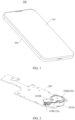
- the electronic device 500 includes a housing 300, a display screen 310, a circuit board assembly 200, and an electronic component 320.
- the display screen 310 is mounted on the housing 300, and encloses an accommodating space (not shown in the figure) with the housing 300.
- Both the circuit board assembly 200 and the electronic component 320 are located in the accommodating space and fixedly connected to the housing 300, and the electronic component 320 is electrically connected to the circuit board assembly 200.
- the electronic component 320 is a motor.
- the electronic component 320 may alternatively be a speaker or another electronic component.
- the electronic component 320 may be a first component (not shown in the figure), or may be a second component 320b.
- the electronic component 320 shown in FIG. 2 is the second component 320b.
- the first component includes a first body, a first circuit board, and a first electrode (not shown in the figure).
- the first circuit board is a flexible printed circuit (Flexible Printed Circuit, FPC).
- the first electrode includes a first positive electrode and a first negative electrode. The first positive electrode and the first negative electrode are arranged side by side and spaced apart, and both the first positive electrode and the first negative electrode are arranged on the first circuit board and electrically connected to the first circuit board.
- the first circuit board is fixedly connected and electrically connected to the first body.
- the first electrode is configured to be electrically connected to the main board, so that the first component is electrically connected to the main board.
- the second component 320b includes a second body 3201b, a second circuit board 3202b, and a second electrode (not marked in the figure).
- the second electrode includes a second positive electrode and a second negative electrode.
- the second positive electrode and the second negative electrode are arranged side by side and spaced apart, and both the second positive electrode and the second negative electrode are arranged on the second circuit board 3202b, and electrically connected to the second circuit board 3202b.
- the second circuit board 3202b is fixedly connected and electrically connected to the second body 3201b.
- the second electrode is configured to be electrically connected to the main board, so that the second component 320b is electrically connected to the main board.
- the second component 320b and the first component may be a same type of electronic component in which a circuit board direction is inconsistent with an electrode direction, or may be different types of electronic components.
- a difference between the second component 320b and the first component lies in that a position of the first circuit board relative to the first body is different from a position of the second circuit board 3202b relative to the second body 3201b, and orientations of the first electrode and the second electrode are different.
- the first circuit board and the second circuit board 3202b are mirror symmetrical structures, and the first electrode and the second electrode are mirror symmetrical structures. In other words, when the first component and the second component 320b are mounted on the circuit board assembly 200, the first electrode and the second electrode correspond to different positions on the circuit board.
- the circuit board assembly 200 includes a circuit board 100 and an elastic piece 110.
- the circuit board 100 includes a main board 101 and a solder pad 102.
- the solder pad 102 is arranged on a surface of the main board 101, and is electrically connected to the main board 101.
- the elastic piece 110 is soldered onto the solder pad 102, and is fixedly connected and electrically connected to the solder pad 102.
- the elastic piece 110 is configured to be electrically connected to the electronic component 320, so that the electronic component 320 is electrically connected to the main board 101.
- the elastic piece 110 may be a first elastic piece 110a or a second elastic piece 110b.
- the electronic component 320 is the second component 320b
- the elastic piece 110 is the second elastic piece 110b.
- the second elastic piece 110b includes a second positive elastic piece 1103 and a second negative elastic piece 1104. Both the second positive elastic piece 1103 and the second negative elastic piece 1104 are fixedly connected and electrically connected to the solder pad 102, and the second positive elastic piece 1103 and the second negative elastic piece 1104 are arranged side by side and spaced apart.
- the second positive elastic piece 1103 is configured to be electrically connected to the second positive electrode of the second component 320b
- the second negative elastic piece 1104 is configured to be electrically connected to the second negative electrode, so that the second component 320b is electrically connected to the main board 101.
- the electronic component 320 is the first component
- the elastic piece 110 is the first elastic piece 110a.
- the first elastic piece 110a includes a first positive elastic piece 1101 and a first negative elastic piece 1102. Both the first positive elastic piece 1101 and the first negative elastic piece 1102 are fixedly connected and electrically connected to the solder pad 102, and the first positive elastic piece 1101 and the first negative elastic piece 1102 are arranged side by side and spaced apart.
- the first positive elastic piece 1101 is configured to be electrically connected to the first positive electrode of the first component
- the first negative elastic piece 1102 is configured to be electrically connected to the first negative electrode, so that the first component is electrically connected to the main board 101.
- circuit board 100 The following specifically describes the structure of the circuit board 100.
- the circuit board 100 includes the main board 101 and the solder pad 102.
- the solder pad 102 is arranged on the main board 101, and is fixedly connected and electrically connected to the main board 101.
- the main board 101 is a printed circuit board (Printed Circuit Board, PCB).
- the main board 101 may alternatively be a flexible circuit board.
- the main board 101 includes a first surface 103 and a second surface 104.
- the first surface 103 is arranged opposite to the second surface 104.
- the main board 101 is provided with a mounting groove 105.
- the mounting groove 105 is provided on a side surface of the main board 101, and runs through the first surface 103 and the second surface 104.
- the mounting groove 105 is configured to mount the electronic component 320.
- a circuit is arranged on the main board 101.
- the circuit includes a positive electrode circuit and a negative electrode circuit (which are not shown in the figure).
- the solder pad 102 is arranged on the first surface 103 of the main board 101, and is electrically connected to the circuit of the main board 101.
- the solder pad 102 includes a first type of solder pad 10, a second type of solder pad 20, a third type of solder pad 30, and a fourth type of solder pad 40.
- the first type of solder pad 10 and the third type of solder pad 30 are arranged side by side and spaced apart. In this embodiment, both an outer contour of the first type of solder pad 10 and an outer contour of the third type of solder pad 30 are rectangular. In other embodiments, the outer contour of the first type of solder pad 10 and the outer contour of the third type of solder pad 30 may alternatively be elliptical, circular, T-shaped, or may be in another shape.
- the first type of solder pad 10 and the third type of solder pad 30 are configured to be simultaneously connected to the first component.
- the second type of solder pad 20 and the fourth type of solder pad 40 are arranged side by side and spaced apart. In this embodiment, both an outer contour of the second type of solder pad 20 and an outer contour of the fourth type of solder pad 40 are T-shaped. In other implementations, the outer contour of the second type of solder pad 20 and the outer contour of the fourth type of solder pad 40 may alternatively be rectangular, elliptical, or may be in another shape. The second type of solder pad 20 and the fourth type of solder pad 40 are configured to be simultaneously connected to the second component 320b.
- the first common solder pad 1 is located between the first sub-solder pad 111 and the second sub-solder pad 112, and is spaced apart from the first sub-solder pad 111 and the second sub-solder pad 112.
- a first gap is provided between the first solder pad 11 and the first common solder pad 1.
- the first gap includes a first sub-gap 13 and a second sub-gap 14.
- the first sub-gap 13 is a gap between the first sub-solder pad 111 and the first common solder pad 1.
- a width of the first sub-gap 13 ranges from 0.15 mm to 0.25 mm.
- the second sub-gap 14 is a gap between the second sub-solder pad 112 and the first common solder pad 1, and a width of the second sub-gap 14 ranges from 0.15 mm to 0.25 mm.
- the first sub-gap 13 and the second sub-gap 14 surround the first side 1a of the first common solder pad 1. It may be understood that the first sub-gap 13 and the second sub-gap 14 separate the first type of solder pad 10 into the first sub-solder pad 111, the second sub-solder pad 112, and the first common solder pad 1.
- Both the first solder pad 11 and the first common solder pad 1 are solders.
- the solder is a tin solder.
- a material of the solder may alternatively be copper or silver.
- Both the first sub-gap 13 and the second sub-gap 14 are filled with a solder resist.
- the gaps are provided between the first solder pad 11 and the first common solder pad 1, and the solder resist is arranged in the gaps, so that the first solder pad 11 can be separated from the first common solder pad 1, thereby preventing the solder from flowing between the first solder pad 11 and the first common solder pad 1.
- a proportion of a total area of the first solder pad 11 and the first common solder pad 1 to a total area of the first solder pad 11, the first common solder pad 1, the first sub-gap 13, and the second sub-gap 14 is greater than or equal to 80%.
- a total area of the first sub-gap 13 and the second sub-gap 14 is less than or equal to 20% of the total area of the first solder pad 11, the first common solder pad 1, the first sub-gap 13, and the second sub-gap 14.
- the total area of the first solder pad 11, the first common solder pad 1, the first sub-gap 13, and the second sub-gap 14 is an original area of the first type of solder pad 10
- the total area of the first solder pad 11 and the first common solder pad 1 is an area occupied by the solder after the first type of solder pad 10 is separated, that is, a soldering area.
- the soldering area of the first type of solder pad 10 is set to at least 80% of the original area of the first type of solder pad 10, so that soldering strength can be ensured.
- the second type of solder pad 20 includes the first common solder pad 1, a second common solder pad 2, and a second solder pad 21.
- the second solder pad 21 is located on the second side 1b of the first common solder pad 1, and is spaced apart from the first common solder pad 1.
- the second solder pad 21 includes a first extending body 211 and a second extending body 212.
- the first extending body 211 is fixedly connected to the second extending body 212.
- the first common solder pad 1 and the second common solder pad 2 are arranged side by side and spaced apart in a length direction of the second type of solder pad 20, the second common solder pad 2 and the first extending body 211 are arranged side by side in a width direction of the third type of solder pad 30, and the second extending body 212 is located between the first common solder pad 1 and the second common solder pad 2.
- a third gap 22 is provided between the second solder pad 21 and the first common solder pad 1.
- a width of the third gap 22 ranges from 0.15 mm to 0.25 mm.
- a fourth gap 23 is provided between the second solder pad 21 and the second common solder pad 2.
- a width of the fourth gap 23 ranges from 0.15 mm to 0.25 mm. It may be understood that the third gap 22 and the fourth gap 23 separate the second type of solder pad 20 into the second solder pad 21, the first common solder pad 1, and the second common solder pad 2.
- the first common solder pad 1, the second common solder pad 2, and the second solder pad 21 are all solders. Both the third gap 22 and the fourth gap 23 are filled with the solder resist.
- gaps are provided between the second solder pad 21 and the first common solder pad 1 and between the second solder pad 21 and the second common solder pad 2, and the solder resist is arranged in the gaps, so that the second solder pad 21 can be separated from the first common solder pad 1 and the second common solder pad 2, thereby preventing the solder from flowing between the second solder pad 21 and the first common solder pad 1 or flowing between the second solder pad 21 and the second common solder pad 2.
- a total area of the second solder pad 21, the first common solder pad 1, and the second common solder pad 2 is an actual soldering area of the second type of solder pad 20.
- a total area of the second solder pad 21, the first common solder pad 1, the second common solder pad 2, the third gap 22, and the fourth gap 23 is an original area of the second type of solder pad 20.
- a soldering area of the second type of solder pad 20 is at least 80% of the original area of the second type of solder pad 20, so that the soldering strength can be ensured.
- a total area of the third gap 22 and the fourth gap 23 is less than or equal to 20% of the total area of the first common solder pad 1, the second solder pad 21, the second common solder pad 2, the third gap 22, and the fourth gap 23.
- the first common solder pad 1 is arranged, and the first common solder pad 1 is used as both a part of the first type of solder pad 10 and a part of the second type of solder pad 20, so that an area of the solder pad 102 can be reduced.
- a region in which the first solder pad 11 and the first common solder pad 1 are located is a first region, and a region in which the second solder pad 21, the first common solder pad 1, and the second common solder pad 2 are located is a second region.
- the first region and the second region have different lengths and widths. In other embodiments, the first region and the second region may have different lengths and a same width; or have a same width and different lengths.
- the third type of solder pad 30 includes a third solder pad 31, the second common solder pad 2, and a third common solder pad 3.
- the third solder pad 31 includes a seventh sub-solder pad 311 and an eighth sub-solder pad 312.
- the seventh sub-solder pad 311, the third common solder pad 3, the eighth sub-solder pad 312, and the second common solder pad 2 are spaced apart in a length direction of the third type of solder pad 30.
- a first clearance 32 is provided between the seventh sub-solder pad 311 and the third common solder pad 3.
- a width of the first clearance 32 ranges from 0.15 mm to 0.25 mm.
- a second clearance 33 is provided between the eighth sub-solder pad 312 and the third common solder pad 3.
- a width of the second clearance 33 ranges from 0.15 mm to 0.25 mm.
- a third clearance 34 is provided between the second common solder pad 2, and the third common solder pad 3 and the eighth sub-solder pad 312.
- a width of the third clearance 34 ranges from 0.15 mm to 0.25 mm. It may be understood that, the first clearance 32, the second clearance 33, and the third clearance 34 separate the third type of solder pad 30 into four parts: the seventh sub-solder pad 311, the second common solder pad 2, the eighth sub-solder pad 312, and the third common solder pad 3.
- the third solder pad 31, the second common solder pad 2, and the third common solder pad 3 are all solders. All the first clearance 32, the second clearance 33, and the third clearance 34 are filled with the solder resist.
- the clearances are arranged between the third solder pad 31, the second common solder pad 2, and the third common solder pad 3, and the solder resist is arranged in the clearances, so that the third solder pad 31, the second common solder pad 2, and the third common solder pad 3 can be separated, thereby preventing the solder from flowing between any two adjacent regions of the third solder pad 31, the second common solder pad 2, and the third common solder pad 3.
- a total area of the first clearance 32, the second clearance 33, and the third clearance 34 is less than or equal to 20% of the total area of the third solder pad 31, the second common solder pad 2, the third common solder pad 3, the first clearance 32, the second clearance 33, and the third clearance 34.
- the length direction of the third type of solder pad 30 is parallel to the length direction of the first type of solder pad 10, and is arranged side by side with and spaced apart from the first type of solder pad 10.
- the length direction of the third type of solder pad 30 intersects with the length direction of the second type of solder pad 20.
- the second common solder pad 2 is the solder pad 102 shared by the second type of solder pad 20 and the third type of solder pad 30. In other words, the second common solder pad 2 is used as both a part of the second type of solder pad 20 and a part of the third type of solder pad 30.
- the second common solder pad 2, the first common solder pad 1, and the second solder pad 21 are configured to be simultaneously connected to the second component 320b.
- the second common solder pad 2, the third common solder pad 3, and the third solder pad 31 are configured to be simultaneously connected to the first component.
- the second common solder pad 102 is arranged, and the second common solder pad 102 is used as both a part of the second type of solder pad 20 and a part of the third type of solder pad 30, so that the area of the solder pad 102 can be reduced.
- the fourth type of solder pad 40 includes the third common solder pad 3 and a fourth solder pad 41.
- the fourth solder pad 41 includes a fifth sub-solder pad 411 and a sixth sub-solder pad 412.
- the fifth sub-solder pad 411, the third common solder pad 3, and the sixth sub-solder pad 412 are spaced apart in a length direction of the fourth type of solder pad 40, and the third common solder pad 3 is located between the fifth sub-solder pad 411 and the sixth sub-solder pad 412.
- a fourth clearance 42 is provided between the fifth sub-solder pad 411 and the third common solder pad 3.
- a width of the fourth clearance 42 ranges from 0.15 mm to 0.25 mm.
- a fifth clearance 43 is provided between the sixth sub-solder pad 412 and the third common solder pad 3. The width of the fifth clearance 43 ranges from 0.15 mm to 0.25 mm.
- Both the third common solder pad 3 and the fourth solder pad 41 are solders. Both the fourth clearance 42 and the fifth clearance 43 are filled with the solder resist.
- the clearances are provided between the fourth solder pad 41 and the third common solder pad 3, and the solder resist is arranged in the clearances, so that the fourth solder pad 41 and the third common solder pad 3 can be separated, thereby preventing the solder from flowing between the fourth solder pad 41 and the third common solder pad 3.
- a total area of the fourth solder pad 41 and the third common solder pad 3 is an actual soldering area of the fourth type of solder pad 40.
- a total area of the fourth solder pad 41, the third common solder pad 3, the fourth clearance 42, and the fifth clearance 43 is an original area of the fourth type of solder pad 40.
- a soldering area of the fourth type of solder pad 40 is at least 80% of the original area of the fourth type of solder pad 40, so that the soldering strength can be ensured.
- a total area of the fourth clearance 42 and the fifth clearance 43 is less than or equal to 20% of the total area of the fourth solder pad 41, the third common solder pad 3, the fourth clearance 42, and the fifth clearance 43.
- the length direction of the fourth type of solder pad 40 is parallel to the length direction of the second type of solder pad 20, and is arranged side by side with and spaced apart from the second type of solder pad 20.
- the length direction of the fourth type of solder pad 40 intersects with the length direction of the third type of solder pad 30.
- the third common solder pad 3 is the solder pad 102 shared by the third type of solder pad 30 and the fourth type of solder pad 40. In other words, the third common solder pad 3 is used as both a part of the third type of solder pad 30 and a part of the fourth type of solder pad 40.
- the third common solder pad 3 and the fourth solder pad 41 are configured to be simultaneously connected to the second component 320b.
- the third common solder pad 3, the second common solder pad 2, and the third solder pad 31 are configured to be simultaneously connected to the first component.
- the third common solder pad 3 is arranged, and the third common solder pad 3 is used as both a part of the third type of solder pad 30 and a part of the fourth type of solder pad 40, so that the area of the solder pad 102 can be reduced.
- the first type of solder pad 10 and the third type of solder pad 30 are configured to be simultaneously connected to the first component.
- the second solder pad 21 and the fourth solder pad 41 are vacant.
- the second type of solder pad 20 and the fourth type of solder pad 40 are configured to be simultaneously connected to the second component 320b.
- the first solder pad 11 and the third solder pad 31 are vacant.
- This embodiment may be implemented in the following implementations.
- the elastic piece 110 is the first elastic piece 110a.
- the first positive elastic piece 1101 is soldered onto the first type of solder pad 10, and the first negative elastic piece 1102 is soldered onto the third type of solder pad 30.
- the first positive electrode of the first component is electrically connected to the first positive elastic piece 1101, and the first negative electrode is electrically connected to the first negative elastic piece 1102.
- the first positive elastic piece 1101 is simultaneously soldered onto the first sub-solder pad 111, the first common solder pad 1, and the second sub-solder pad 112 of the first type of solder pad 10.
- the positive electrode circuit of the main board 101 is conducted to the first positive elastic piece 1101 simultaneously through the first sub-solder pad 111, the second sub-solder pad 112, and the first common solder pad 1, to be conducted to the first positive electrode of the first component.
- the first negative elastic piece 1102 is simultaneously soldered onto the seventh sub-solder pad 311, the eighth sub-solder pad 312, the second common solder pad 2, and the third common solder pad 3 of the third type of solder pad 30.
- the negative electrode circuit of the main board 101 is conducted to the first negative elastic piece 1102 simultaneously through the seventh sub-solder pad 311, the eighth sub-solder pad 312, and the third common solder pad 3, to be conducted to the first negative electrode of the first component, so that the first component is electrically connected to the main board 101.
- the positive electrode circuit of the main board 101 is conducted to the second positive elastic piece 1103 simultaneously through the first common solder pad 1 and the second solder pad 21, to be conducted to the second positive electrode of the second component 320b.
- the second negative elastic piece 1104 is simultaneously soldered onto the fifth sub-solder pad 411, the third common solder pad 3, and the sixth sub-solder pad 412 of the fourth type of solder pad 40.
- the negative electrode circuit of the main board 101 is conducted to the second negative elastic piece 1104 simultaneously through the fifth sub-solder pad 411, the third common solder pad 3, and the sixth sub-solder pad 412, to be conducted to the second negative electrode of the second component 320b, so that the second component 320b is electrically connected to the main board 101.
- the first common solder pad 1, the second common solder pad 2, and the third common solder pad 3 are arranged.
- the first type of solder pad 10 and the second type of solder pad 20 share the first common solder pad 1
- the second type of solder pad 20 and the third type of solder pad 30 share the second common solder pad 2
- the third type of solder pad 30 and the fourth type of solder pad 40 share the third common solder pad 3.
- the solder pad 102 is segmented, so that two different elastic pieces 110 can be soldered onto the solder pad 102. In this way, the same main board 101 can be electrically connected to two different electronic components 320, the area of the solder pad 102 is reduced, and utilization of the main board 101 is improved, thereby reducing costs.
- an area of each type of solder pad 102 is approximately the same as an area of the corresponding elastic piece 110, and the solder pad 102 is separated, so that a large deviation in a soldering position caused by solder floating during soldering can be avoided, accuracy of a soldering position of the elastic piece 110 is improved, and stability of elastic connection of the elastic piece 110 is ensured.
- the second common solder pad 2 is set to be insulated from the main board 101, so that the second common solder pad 2 is used only for fixed connection, and is not conductive, thereby avoiding a short circuit in the second common solder pad 2 when the second type of solder pad 20 is electrically connected to the positive electrode circuit, and the third type of solder pad 30 is electrically connected to the negative electrode circuit.
- a difference between this implementation and the first implementation lies in that the first sub-solder pad 111, the second sub-solder pad 112, the first common solder pad 1, and the second solder pad 21 are all electrically connected to the negative electrode circuit of the main board 101, and are used as the negative electrode of the main board 101.
- the seventh sub-solder pad 311, the eighth sub-solder pad 312, the fifth sub-solder pad 411, the sixth sub-solder pad 412, and the third common solder pad 3 are all electrically connected to the positive electrode circuit of the main board 101, and are used as the positive electrode of the main board 101.
- the second common solder pad 2 is insulated from the main board 101.
- the first positive elastic piece 1101 is soldered onto the third type of solder pad 30, and the first negative elastic piece 1102 is soldered onto the first type of solder pad 10.
- the second positive elastic piece 1103 is soldered onto the fourth type of solder pad 40, and the second negative elastic piece 1104 is soldered onto the second type of solder pad 20.
- the first common solder pad 1 is electrically connected to the positive electrode circuit of the main board 101, and is used as the positive electrode of the main board 101.
- the third common solder pad 3 is electrically connected to the negative electrode circuit of the main board 101, and is used as the negative electrode of the main board 101.
- the first solder pad 11, the second solder pad 21, the third solder pad 31, the fourth solder pad 41, and the second common solder pad 2 are all insulated from the main board 101, are neither used as the positive electrode of the main board 101 nor used as the negative electrode of the main board 101, and is used for fixed connection.
- the first positive elastic piece 1101 is soldered onto the first type of solder pad 10
- the first negative elastic piece 1102 is soldered onto the third type of solder pad 30.
- the positive electrode circuit of the main board 101 is conducted to the first positive elastic piece 1101 through the first common solder pad 1, to be conducted to the first positive electrode of the first component.
- the negative electrode circuit of the main board 101 is conducted to the first negative elastic piece 1102 through the third common solder pad 3, to be conducted to the first negative electrode of the first component, so that the first component is electrically connected to the main board 101.
- the second positive elastic piece 1103 is soldered onto the second type of solder pad 20, and the second negative elastic piece 1104 is soldered onto the fourth type of solder pad 40.
- the positive electrode circuit of the main board 101 is conducted to the second positive elastic piece 1103 through the first common solder pad 1, to be conducted to the second positive electrode of the second component 320b.
- the negative electrode circuit of the main board 101 is conducted to the second negative elastic piece 1104 through the third common solder pad 3, to be conducted to the second negative electrode of the second component 320b, so that the second component 320b is electrically connected to the main board 101.
- the first common solder pad 1 and the third common solder pad 3 are used as electrical connection regions, and other regions are only used as fixed connection regions, so that the first common solder pad 1 can electrically connect the first positive elastic piece 1101 to the main board 101, and electrically connect the second positive elastic piece 1103 to the main board 101.
- the third common solder pad 3 can electrically connect the first negative elastic piece 1102 to the main board 101 and electrically connect the second negative elastic piece 1104 to the main board 101, thereby simplifying the structure of the solder pad 102.
- FIG. 7 is a schematic diagram of a partial structure of a circuit board 100 according to Embodiment 2 of this application.
- solder pad 102 includes the first type of solder pad 10 and the second type of solder pad 20.
- the first type of solder pad 10 includes the first solder pad 11 and the first common solder pad 1.
- the second type of solder pad 20 includes the first common solder pad 1 and the second solder pad 21.
- the length direction of the first type of solder pad 10 is parallel to the length direction of the second type of solder pad 20.
- the first common solder pad 1 includes the first side 1a and the second side 1b. The first side 1a and the second side 1b are arranged oppositely.
- the first solder pad 11, the first common solder pad 1, and the second solder pad 21 are arranged side by side and spaced apart in the length direction of the first type of solder pad 10, and the first common solder pad 1 is located between the first solder pad 11 and the second solder pad 21.
- the first solder pad 11 is located on the first side 1a
- the second solder pad 21 is located on the second side 1b. That is, the first solder pad 11, the first common solder pad 1, and the second solder pad 21 are arranged in a straight line.
- a width of a gap between the first common solder pad 1 and the first solder pad 11 ranges from 0.15 mm to 0.25 mm
- a width of a gap between the first common solder pad 1 and the second solder pad 21 ranges from 0.15 mm to 0.25 mm.
- Both the gap between the first common solder pad 1 and the first solder pad 11 and the gap between the first common solder pad 1 and the second solder pad 21 are filled with the solder resist, to separate the first common solder pad 1 from the first solder pad 11 and the second solder pad 21, preventing the solder from flowing between the first common solder pad 1 and the first solder pad 11 and between the first common solder pad 1 and the second solder pad 21.
- the second positive elastic piece 1103 is simultaneously soldered onto and electrically connected to the second solder pad 21 and the first common solder pad 1, and the second positive electrode of the second component 320b is conducted to the second negative elastic piece 1104, so that the second component 320b is electrically connected to the main board 101.
- the first common solder pad 1 is arranged, and the first common solder pad 1 is used as both a part of the first type of solder pad 10 and a part of the second type of solder pad 20, so that the area of the solder pad 102 can be reduced.
- the first common solder pad 1 and the first solder pad 11 may be configured to be connected to the first component
- the first common solder pad 1 and the second solder pad 21 may be configured to be connected to the second component 320b, so that the same main board 101 can be electrically connected to two different electronic components 320, and utilization of the main board 101 is improved, thereby reducing costs.
- first common solder pad 1 is spaced apart from both the first solder pad 11 and the second solder pad 21, so that the large deviation in the soldering position caused by the solder floating during soldering can be avoided, the accuracy of the soldering position of the elastic piece 110 is improved, and the stability of the elastic connection of the elastic piece 110 is ensured.
- a difference between this implementation and the first implementation lies in that the first solder pad 11, the first common solder pad 1, and the second solder pad 21 are all electrically connected to the negative electrode circuit of the main board 101, and are used as the negative electrode of the main board 101.
- the first negative elastic piece 1102 is simultaneously soldered onto and electrically connected to the first solder pad 11 and the first common solder pad 1.
- the second negative elastic piece 1104 is simultaneously soldered onto and electrically connected to the second solder pad 21 and the first common solder pad 1.
- the first common solder pad 1 is electrically connected to the positive electrode circuit of the main board 101, and is used as the positive electrode of the main board 101. Both the first solder pad 11 and the second solder pad 21 are insulated from the main board 101.
- the first positive elastic piece 1101 is soldered onto the first type of solder pad 10, and is electrically connected to the first common solder pad 1, so that the main board 101 is conducted to the first positive electrode of the first component.
- the second positive elastic piece 1103 is soldered onto the second type of solder pad 20, and is electrically connected to the first common solder pad 1, so that the main board 101 is conducted to the second positive electrode of the second component 320b.
- a difference between this implementation and the third implementation lies in that the first common solder pad 1 is electrically connected to the negative electrode circuit of the main board 101, and is used as the negative electrode of the main board 101. Both the first solder pad 11 and the second solder pad 21 are insulated from the main board 101.
- the first solder pad 11 is electrically connected to the positive electrode circuit of the main board 101, and is used as the positive electrode of the main board 101.
- the second solder pad 21 is electrically connected to the negative electrode circuit of the main board 101, and is used as the negative electrode of the main board 101.
- the first common solder pad 1 is insulated from the main board 101.
- the second negative elastic piece 1104 is soldered onto the second solder pad 21 and the second common solder pad 2, and is electrically connected to the second solder pad 21.
- the second negative electrode of the second component 320b is electrically connected to the second negative elastic piece 1104, so that the second component 320b is electrically connected to the main board 101.
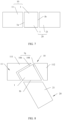
- FIG. 8 is a schematic diagram of a partial structure of a circuit board 100 according to Embodiment 3 of this application.
- a difference between this embodiment and Embodiment 2 lies in that, in this embodiment, the length direction of the first type of solder pad 10 intersects with the length direction of the second type of solder pad 20.
- the first type of solder pad 10 includes the first sub-solder pad 111 and the second sub-solder pad 112.
- the first common solder pad 1 includes the first side 1a and the second side 1b.
- the first side 1a includes a first sub-side 106 and a second sub-side 108.
- the first sub-solder pad 111 is located on the first sub-side 106
- the second sub-solder pad 112 is located on the second sub-side 108.
- the first positive elastic piece 1101 is electrically connected to the first positive electrode of the first component, so that the first component is electrically connected to the main board 101.
- the second positive elastic piece 1103 is simultaneously soldered onto and electrically connected to the second solder pad 21 and the first common solder pad 1.
- the second positive elastic piece 1103 is electrically connected to the second positive electrode of the second component 320b, so that the second component 320b is electrically connected to the main board 101.
- the first sub-solder pad 111, the second sub-solder pad 112, the first common solder pad 1, and the second solder pad 21 may alternatively be all electrically connected to the negative electrode circuit of the main board 101.
- the first common solder pad 1 is electrically connected to the positive electrode circuit or the negative electrode circuit of the main board 101, and the first sub-solder pad 111, the second sub-solder pad 112, and the second solder pad 21 are insulated from the main board 101.
- both the first sub-solder pad 111 and the second sub-solder pad 112 are electrically connected to the positive electrode circuit of the main board 101
- the second solder pad 21 is electrically connected to the negative electrode circuit of the main board 101
- the first common solder pad 1 is insulated from the main board 101
- the first type of solder pad 10 is configured to be connected to the first positive elastic piece 1101
- the second type of solder pad 20 is configured to be connected to the second negative elastic piece 1104.
- the first common solder pad 1 is arranged, and the first common solder pad 1 is used as both a part of the first type of solder pad 10 and a part of the second type of solder pad 20, so that the area of the solder pad 102 can be reduced.
- the first common solder pad 1 and the first solder pad 11 may be configured to be connected to the first component
- the first common solder pad 1 and the second solder pad 21 may be configured to be connected to the second component 320b, so that the same main board 101 can be electrically connected to two different electronic components 320, and utilization of the main board 101 is improved, thereby reducing costs.
- the length direction of the first type of solder pad 10 intersects with the length direction of the second type of solder pad 20, so that the solder pad 102 can be applied to two different electronic components 320, thereby improving utilization of the circuit board 100.
- FIG. 9 is a schematic diagram of a partial structure of a circuit board 100 according to Embodiment 4 of this application.
- the second sub-solder pad 112 is located on a side close to the second sub-side 108, and is spaced apart from the second sub-side 108.
- the third sub-solder pad 213, the first common solder pad 1, and the fourth sub-solder pad 214 are arranged side by side and spaced apart.
- the third sub-solder pad 213 is located on a side of the first common solder pad 1 close to the third sub-side 107, and is spaced apart from the third sub-side 107.
- the fourth sub-solder pad 214 is located on a side close to the fourth sub-side 109, and is spaced apart from the fourth sub-side 109.
- the first sub-solder pad 111, the first common solder pad 1, and the second sub-solder pad 112 are configured to be simultaneously connected to the first component.
- the third sub-solder pad 213 and the fourth sub-solder pad 214 are vacant.
- the third sub-solder pad 213, the fourth sub-solder pad 214, and the first common solder pad 1 are configured to be simultaneously connected to the second component 320b.
- the first sub-solder pad 111 and the second sub-solder pad 112 are vacant.
- the first common solder pad 1 is arranged, and the first common solder pad 1 is used as both a part of the first type of solder pad 10 and a part of the second type of solder pad 20, so that the area of the solder pad 102 can be reduced.
- the first common solder pad 1 and the first solder pad 11 may be configured to be connected to the first component
- the first common solder pad 1 and the second solder pad 21 may be configured to be connected to the second component 320b, so that the same main board 101 can be electrically connected to two different electronic components 320, and utilization of the main board 101 is improved, thereby reducing costs.
- the length direction of the first type of solder pad 10 intersects with the length direction of the second type of solder pad 20, so that the solder pad 102 can be applied to two different electronic components 320, thereby improving utilization of the circuit board 100.
- the first common solder pad 1 is spaced apart from both the first solder pad 11 and the second solder pad 21, so that the large deviation in the soldering position caused by the solder floating during soldering can be avoided, the accuracy of the soldering position of the elastic piece 110 is improved, and the stability of the elastic connection of the elastic piece 110 is ensured.
Landscapes
- Engineering & Computer Science (AREA)
- Microelectronics & Electronic Packaging (AREA)
- Combinations Of Printed Boards (AREA)
- Electric Connection Of Electric Components To Printed Circuits (AREA)
Abstract
Description
- This application claims priority to Patent Application No.
202210938637.X, filed with the China National Intellectual Property Administration on August 5, 2022 - This application relates to the field of communication technologies, and in particular, to a circuit board, a circuit board assembly, and an electronic device.
- In an electronic device such as a mobile phone, a main board is generally in elastic conduction with electronic components such as a motor and a speaker through elastic pieces, and positions of a solder pad and the elastic piece on the main board and a corresponding electronic component are relatively fixed in matching positions. When two electronic components such as motors are provided and have different directions, corresponding positions of the elastic pieces on the main board are different, so that different main boards are required to adapt to different electronic components, resulting in low utilization of the main board.
- This application provides a circuit board, a circuit board assembly, and an electronic device, to resolve a technical problem of low utilization of a main board in the related art.
- This application provides a circuit board. The circuit board is configured to arrange a first component or a second component. The circuit board includes a main board, a first type of solder pad, and a second type of solder pad. Both the first type of solder pad and the second type of solder pad are formed on a surface of the main board, and are electrically connected to the main board. The first type of solder pad includes a first solder pad and a first common solder pad, and the second type of solder pad includes a second solder pad and the first common solder pad. The first common solder pad includes a first side and a second side, and the first solder pad and the second solder pad are respectively located on the first side and the second side, and are spaced apart from the first common solder pad. The first solder pad and the first common solder pad are configured to be simultaneously connected to the first component, and the second solder pad and the first common solder pad are configured to be simultaneously connected to the second component.
- In this embodiment, the first common solder pad is arranged, and the first common solder pad is used as both a part of the first type of solder pad and a part of the second type of solder pad, so that an area of a solder pad area can be reduced. In addition, when jointly used, the first common solder pad and the first solder pad may be configured to be connected to the first component, and when jointly used, the first common solder pad and the second solder pad may be configured to be connected to the second component, so that a same main board can be electrically connected to two different electronic components, and utilization of the main board is improved, thereby reducing costs. In addition, the first common solder pad is spaced apart from both the first solder pad and the second solder pad, so that a large deviation in a soldering position caused by solder floating during soldering can be avoided, accuracy of a soldering position of the elastic piece is improved, and stability of elastic connection of the elastic piece is ensured.
- In a possible implementation, when the first solder pad and the first common solder pad are configured to be simultaneously connected to the first component, the second solder pad is vacant, and when the second solder pad and the first common solder pad are configured to be simultaneously connected to the second component, the first solder pad is vacant.
- In this embodiment, when jointly used, the first common solder pad and the first solder pad may be configured to be connected to the first component, and when jointly used, the first common solder pad and the second solder pad may be configured to be connected to the second component, so that a same main board can be electrically connected to two different electronic components, and utilization of the main board is improved, thereby reducing costs.
- In a possible implementation, a first gap is provided between the first solder pad and the first common solder pad, and an area of the first gap is less than or equal to 20% of a total area of the first solder pad, the first gap, and the first common solder pad.
- It may be understood that the total area of the first solder pad, the first common solder pad, and the first gap is an original area of the first type of solder pad, and a total area of the first solder pad and the first common solder pad is an area occupied by a solder after the first type of solder pad is separated, that is, a soldering area. In this embodiment, the area of the first gap is less than or equal to 80% of the original area of the first type of solder pad. In other words, the soldering area of the first type of solder pad is set to be at least 80% of the original area of the first type of solder pad, thereby ensuring soldering strength.
- In a possible implementation, a width of the first gap ranges from 0.15 mm to 0.25 mm. In this embodiment, the first gap is provided between the first solder pad and the first common solder pad, to prevent the solder from flowing between the first solder pad and the first common solder pad. In addition, when the first common solder pad is used as the second type of solder pad, when the elastic piece is soldered onto the second type of solder pad, a large deviation in a soldering position caused by drifting of the elastic piece toward the first solder pad can also be avoided. Therefore, the accuracy of the soldering position of the elastic piece is improved, and the stability of the elastic connection of the elastic piece is ensured, so that stability of an electrical connection between the electronic component and the main board is ensured.
- In a possible implementation, a solder resist is arranged on the surface of the main board, and the solder resist is located in the first gap. In this embodiment, the first gap is filled with the solder resist, to prevent the solder from flowing between the first solder pad and the first common solder pad.
- In a possible implementation, a length direction of the first type of solder pad intersects with a length direction of the second type of solder pad. In this embodiment, the length direction of the first type of solder pad intersects with the length direction of the second type of solder pad, so that the solder pad can be applied to two electronic components with different electrode directions, thereby further improving utilization of the circuit board.
- In a possible implementation, the first solder pad includes a first sub-solder pad and a second sub-solder pad, the first sub-solder pad. The first common solder pad, and the second sub-solder pad are arranged side by side and spaced apart in the length direction of the first type of solder pad. The first common solder pad is located between the first sub-solder pad and the second sub-solder pad. The first side includes a first sub-side and a second sub-side. The first sub-solder pad is located on the first sub-side, and the second sub-solder pad is located on the second sub-side.
- In this embodiment, the first solder pad is segmented into the first sub-solder pad and the second sub-solder pad, so that a distribution range of the first solder pad is increased, thereby improving adaptability of the first solder pad to the first component. In addition, in this embodiment, both the first sub-solder pad and the second sub-solder pad are spaced apart from the first common solder pad, so that the large deviation in the soldering position caused by solder floating during soldering can be avoided, the accuracy of the soldering position of the elastic piece is improved, and the stability of the elastic connection of the elastic piece is ensured.
- In a possible implementation, the second solder pad includes a third sub-solder pad and a fourth sub-solder pad. The third sub-solder pad, the first common solder pad, and the fourth sub-solder pad are arranged side by side and spaced apart in the length direction of the second type of solder pad. The first common solder pad is located between the third sub-solder pad and the fourth sub-solder pad. The second side includes a third sub-side and a fourth sub-side. The third sub-solder pad is located on the third sub-side, and the fourth sub-solder pad is located on the fourth sub-side.
- In this embodiment, the second solder pad is segmented into the third sub-solder pad and the fourth sub-solder pad, so that a distribution range of the second solder pad can be increased, thereby improving adaptability of the second solder pad to the second component.
- In a possible implementation, a length direction of the first type of solder pad is parallel to a length direction of the second type of solder pad; and the first solder pad, the first common solder pad, and the second solder pad are arranged side by side and spaced apart in the length direction of the first type of solder pad, and the first common solder pad is located between the first solder pad and the second solder pad.
- In this embodiment, the first solder pad, the first common solder pad, and the second solder pad are arranged in a straight line, so that the first type of solder pad and the second type of solder pad are applicable to two electronic components having a same electrode extension direction and different positions.
- In a possible implementation, the main board includes a positive electrode circuit and a negative electrode circuit, the first common solder pad is electrically connected to the positive electrode circuit, and both the first solder pad and the second solder pad are insulated from the main board; or the first common solder pad is electrically connected to the negative electrode circuit, and both the first solder pad and the second solder pad are insulated from the main board.
- In this embodiment, the first common solder pad is used as an electrical connection region, and other regions are only used as fixed connection regions, so that when jointly used, the first common solder pad and the first solder pad can be electrically connected to the first component, and when jointly used, the first common solder pad and the second solder pad can be electrically connected to the second component, thereby simplifying a structure of the solder pad.
- In a possible implementation, the main board includes a positive electrode circuit and a negative electrode circuit, the first solder pad is electrically connected to the positive electrode circuit, the second solder pad is electrically connected to the negative electrode circuit, and the first common solder pad is insulated from the main board; or the first solder pad is electrically connected to the negative electrode circuit, the second solder pad is electrically connected to the positive electrode circuit, and the first common solder pad is insulated from the main board.
- In this embodiment, the first common solder pad is set to be insulated from the main board, so that the first common solder pad is only used for fixed connection, and is not conductive, thereby avoiding a short circuit when the first type of solder pad and the second type of solder pad are separately connected to circuits of different polarities.
- In a possible implementation, the second type of solder pad further includes a second common solder pad. The second common solder pad is spaced apart from the second solder pad and the first common solder pad. The second common solder pad, the second solder pad, and the first common solder pad are configured to be simultaneously connected to the second component. The circuit board further includes a third type of solder pad. The third type of solder pad is formed on the surface of the main board, and is arranged side by side with and spaced apart from the first type of solder pad. The third type of common solder pad includes a third solder pad and the second common solder pad. The third solder pad is spaced apart from the second common solder pad, and the second common solder pad and the third solder pad are configured to be simultaneously connected to the first component.
- In this embodiment, the third type of solder pad is arranged, and the third type of solder pad and the first type of solder pad may be simultaneously connected to the first component. In actual application, the third type of solder pad and the first type of solder pad may be electrically connected to a positive electrode and a negative electrode of the first component respectively. In this way, a current loop is formed between the first component and the main board, so that the first component is electrically connected to the main board. In addition, in this embodiment, the second common solder pad is arranged, so that the second common solder pad is used as both a part of the second type of solder pad and a part of the third type of solder pad, thereby further reducing the area of the solder pad, saving space, and saving materials.
- In a possible implementation, a third gap is provided between the first common solder pad and the second solder pad, and a fourth gap is provided between the second solder pad and the second common solder pad; and a total area of the third gap and the third gap is less than or equal to 20% of a total area of the first common solder pad, the second solder pad, the second common solder pad, the third gap, and the fourth gap.
- In this embodiment, a total area of the second solder pad, the first common solder pad, and the second common solder pad is an actual soldering area of the second type of solder pad. The total area of the second solder pad, the first common solder pad, the second common solder pad, the third gap, and the fourth gap is an original area of the second type of solder pad. In this embodiment, a total area of the third gap and the third gap is less than or equal to 20% of the total area of the first common solder pad, the second solder pad, the second common solder pad, the third gap, and the fourth gap. In other words, a soldering area of the second type of solder pad is at least 80% of the original area of the second type of solder pad, thereby ensuring strength of soldering between the elastic piece and the second type of solder pad.
- In a possible implementation, a region in which the first solder pad and the first common solder pad are located is a first region. A region in which the second solder pad, the first common solder pad, and the second common solder pad are located is a second region. At least one of a length and a width of the first region is different from a length of the second region, or is different from a width of the second region.
- In this embodiment, sizes of the first region and the second region are different, so that the first region and the second region can be adapted to elastic pieces of different sizes, so that the first type of solder pad and the second type of solder pad can be used for soldering different electronic components, thereby improving applicability of the circuit board.
- In a possible implementation, the third type of solder pad further includes a third common solder pad. The third common solder pad is spaced apart from the third solder pad and the second common solder pad. The third common solder pad, the third solder pad, and the second common solder pad are configured to be simultaneously connected to the first component. The circuit board further includes a fourth type of solder pad. The fourth type of solder pad is formed on the surface of the main board, and is arranged side by side with and spaced apart from the second type of solder pad. The fourth type of solder pad includes a fourth solder pad and the third common solder pad. The fourth solder pad is spaced apart from the third common solder pad, and the third common solder pad and the fourth solder pad are configured to be simultaneously connected to the second component.
- In this embodiment, the fourth type of solder pad is arranged, and the fourth type of solder pad and the second type of solder pad may be simultaneously connected to the second component. In actual application, the fourth type of solder pad and the second type of solder pad may be electrically connected to a positive electrode and a negative electrode of the second component respectively. In this way, a current loop is formed between the second component and the main board, so that the second component is electrically connected to the main board. In addition, in this embodiment, the third common solder pad is arranged, so that the third common solder pad is used as both a part of the third type of solder pad and a part of the fourth type of solder pad, thereby further reducing the area of the solder pad, saving the space, and saving the materials.
- In a possible implementation, the main board includes a positive electrode circuit and a negative electrode circuit, the first common solder pad is electrically connected to the positive electrode circuit, the third common solder pad is electrically connected to the negative electrode circuit, and the first solder pad, the second solder pad, the third solder pad, the fourth solder pad, and the third common solder pad are all insulated from the main board; or the first common solder pad is electrically connected to the negative electrode circuit, the third common solder pad is electrically connected to the positive electrode circuit, and the first solder pad, the second solder pad, the third solder pad, the fourth solder pad, and the third common solder pad are all insulated from the main board.
- In this embodiment, the first common solder pad and the third common solder pad are used as electrical connection regions, and other regions are only used as fixed connection regions, so that the first component is electrically connected to the main board, and the second component is electrically connected to the main board, thereby simplifying the structure of the solder pad.
- In a possible implementation, the main board includes a positive electrode circuit and a negative electrode circuit, the first solder pad, the first common solder pad, and the second solder pad are all electrically connected to the positive electrode circuit, the third solder pad, the fourth solder pad, and the third common solder pad are all electrically connected to the negative electrode circuit, and the second common solder pad is insulated from the main board; or the first solder pad, the first common solder pad, and the second solder pad are all electrically connected to the negative electrode circuit, the third solder pad, the fourth solder pad, and the third common solder pad are all electrically connected to the positive electrode circuit, and the second common solder pad is insulated from the main board.
- In this embodiment, when the first component is connected to the first type of solder pad and the third type of solder pad, the first component is electrically connected to the main board through the first solder pad, the first common solder pad, and the third solder pad. When the second component is connected to the second type of solder pad and the fourth type of solder pad, the second component is electrically connected to the main board through the second solder pad, the first common solder pad, and the fourth solder pad. In addition, in this embodiment, the second common solder pad is set to be insulated from the main board, to avoid a short circuit when the second type of solder pad and the third type of solder pad are separately connected to circuits of different polarities.
- In an embodiment, this application provides a circuit board assembly, including an elastic piece and the foregoing circuit board. The elastic piece is a first elastic piece or a second elastic piece. When the elastic piece is the first elastic piece, the first elastic piece is soldered onto the first solder pad and the first common solder pad; or when the elastic piece is the second elastic piece, the second elastic piece is soldered onto the second solder pad and the first common solder pad.
- In this embodiment, when jointly used, the first common solder pad and the first solder pad can be used for soldering the first elastic piece, and when jointly used, the first common solder pad and the second solder pad can be used for soldering the second elastic piece. In other words, the circuit board provided in this embodiment can be used for soldering both the first elastic piece and the second elastic piece, so that utilization of the circuit board can be improved.
- In an embodiment, this application provides an electronic device, including an electronic component and the foregoing circuit board assembly. The electronic component is a first component or a second component. When the elastic piece is the first elastic piece, the electronic component is the first component, and the first component is electrically connected to the first elastic piece; or when the elastic piece is the second elastic piece, the electronic component is the second component, and the second component is electrically connected to the second elastic piece.
- The circuit board in the electronic device provided in this embodiment can be soldered with both the first elastic piece and the second elastic piece, so that the electronic device can select the different first component and second component according to different use scenarios, thereby improving applicability of the electronic device, to improve utilization of the circuit board assembly and reduce costs.
- In conclusion, in this application, a first common solder pad is arranged, and a first common solder pad is used as both a part of a first type of solder pad and a part of a second type of solder pad, so that an area of a solder pad can be reduced. In addition, when jointly used, the first common solder pad and the first solder pad may be configured to be connected to the first component, and when jointly used, the first common solder pad and the second solder pad may be configured to be connected to the second component, so that a same main board can be electrically connected to two different electronic components, and utilization of the main board is improved, thereby reducing costs. In addition, the first common solder pad is spaced apart from both the first solder pad and the second solder pad, so that a large deviation in a soldering position caused by solder floating during soldering can be avoided, accuracy of a soldering position of the elastic piece is improved, and stability of elastic connection of the elastic piece is ensured.
- To describe the technical solutions in the embodiments of this application or the background more clearly, the following briefly describes the accompanying drawings required for describing the embodiments of this application or the background.
-
FIG. 1 is a schematic diagram of a structure of an electronic device according to an embodiment of this application; -
FIG. 2 is a schematic diagram of a partial structure of the electronic device shown inFIG. 1 ; -
FIG. 3 is a schematic diagram of a structure of a circuit board assembly in the electronic device shown inFIG. 1 in a first scenario; -
FIG. 4 is a schematic diagram of a structure of the circuit board assembly shown inFIG. 3 in a second scenario; -
FIG. 5 is a schematic diagram of a structure of a circuit board in the circuit board assembly shown inFIG. 3 ; -
FIG. 6 is a schematic enlarged view of a structure of a solder pad in the circuit board shown inFIG. 5 ; -
FIG. 7 is a schematic diagram of a partial structure of a circuit board according toEmbodiment 2 of this application; -
FIG. 8 is a schematic diagram of a partial structure of a circuit board according toEmbodiment 3 of this application; and -
FIG. 9 is a schematic diagram of a partial structure of a circuit board according to Embodiment 4 of this application. - The following describes the embodiments of this application with reference to the accompanying drawings in the embodiments of this application.
- Refer to
FIG. 1 and FIG. 2. FIG. 1 is a schematic diagram of a structure of anelectronic device 500 according to an embodiment of this application, andFIG. 2 is a schematic diagram of a partial structure of theelectronic device 500 shown inFIG. 1 . - This application provides an
electronic device 500. Theelectronic device 500 includes, but is not limited to, electronic products such as a cellphone (cellphone), a notebook computer (noteBook computer), a tablet personal computer (tablet personal computer), a laptop computer (laptop computer), a personal digital assistant (personal digital assistant, PDA), or a wearable device (wearable device). Descriptions are provided below by using an example in which theelectronic device 500 is a cellphone. - The
electronic device 500 includes ahousing 300, adisplay screen 310, acircuit board assembly 200, and anelectronic component 320. Thedisplay screen 310 is mounted on thehousing 300, and encloses an accommodating space (not shown in the figure) with thehousing 300. Both thecircuit board assembly 200 and theelectronic component 320 are located in the accommodating space and fixedly connected to thehousing 300, and theelectronic component 320 is electrically connected to thecircuit board assembly 200. In this embodiment, theelectronic component 320 is a motor. In other embodiments, theelectronic component 320 may alternatively be a speaker or another electronic component. Theelectronic component 320 may be a first component (not shown in the figure), or may be asecond component 320b. Theelectronic component 320 shown inFIG. 2 is thesecond component 320b. - The first component includes a first body, a first circuit board, and a first electrode (not shown in the figure). The first circuit board is a flexible printed circuit (Flexible Printed Circuit, FPC). The first electrode includes a first positive electrode and a first negative electrode. The first positive electrode and the first negative electrode are arranged side by side and spaced apart, and both the first positive electrode and the first negative electrode are arranged on the first circuit board and electrically connected to the first circuit board. The first circuit board is fixedly connected and electrically connected to the first body. The first electrode is configured to be electrically connected to the main board, so that the first component is electrically connected to the main board.
- The
second component 320b includes asecond body 3201b, asecond circuit board 3202b, and a second electrode (not marked in the figure). The second electrode includes a second positive electrode and a second negative electrode. The second positive electrode and the second negative electrode are arranged side by side and spaced apart, and both the second positive electrode and the second negative electrode are arranged on thesecond circuit board 3202b, and electrically connected to thesecond circuit board 3202b. Thesecond circuit board 3202b is fixedly connected and electrically connected to thesecond body 3201b. The second electrode is configured to be electrically connected to the main board, so that thesecond component 320b is electrically connected to the main board. - The
second component 320b and the first component may be a same type of electronic component in which a circuit board direction is inconsistent with an electrode direction, or may be different types of electronic components. In this embodiment, a difference between thesecond component 320b and the first component lies in that a position of the first circuit board relative to the first body is different from a position of thesecond circuit board 3202b relative to thesecond body 3201b, and orientations of the first electrode and the second electrode are different. In this embodiment, the first circuit board and thesecond circuit board 3202b are mirror symmetrical structures, and the first electrode and the second electrode are mirror symmetrical structures. In other words, when the first component and thesecond component 320b are mounted on thecircuit board assembly 200, the first electrode and the second electrode correspond to different positions on the circuit board. - Refer to
FIG. 3 and FIG. 4. FIG. 3 is a schematic diagram of a structure of thecircuit board assembly 200 in theelectronic device 500 shown inFIG. 1 in a first scenario, andFIG. 4 is a schematic diagram of a structure of thecircuit board assembly 200 shown inFIG. 3 in a second scenario. - The
circuit board assembly 200 includes acircuit board 100 and anelastic piece 110. Thecircuit board 100 includes amain board 101 and asolder pad 102. Thesolder pad 102 is arranged on a surface of themain board 101, and is electrically connected to themain board 101. Theelastic piece 110 is soldered onto thesolder pad 102, and is fixedly connected and electrically connected to thesolder pad 102. Theelastic piece 110 is configured to be electrically connected to theelectronic component 320, so that theelectronic component 320 is electrically connected to themain board 101. Theelastic piece 110 may be a firstelastic piece 110a or a secondelastic piece 110b. - As shown in
FIG. 3 , in the first scenario, theelectronic component 320 is thesecond component 320b, and theelastic piece 110 is the secondelastic piece 110b. In this embodiment, the secondelastic piece 110b includes a second positiveelastic piece 1103 and a second negativeelastic piece 1104. Both the second positiveelastic piece 1103 and the second negativeelastic piece 1104 are fixedly connected and electrically connected to thesolder pad 102, and the second positiveelastic piece 1103 and the second negativeelastic piece 1104 are arranged side by side and spaced apart. The second positiveelastic piece 1103 is configured to be electrically connected to the second positive electrode of thesecond component 320b, and the second negativeelastic piece 1104 is configured to be electrically connected to the second negative electrode, so that thesecond component 320b is electrically connected to themain board 101. - As shown in
FIG. 4 , in the second scenario, theelectronic component 320 is the first component, and theelastic piece 110 is the firstelastic piece 110a. In this embodiment, the firstelastic piece 110a includes a first positiveelastic piece 1101 and a first negativeelastic piece 1102. Both the first positiveelastic piece 1101 and the first negativeelastic piece 1102 are fixedly connected and electrically connected to thesolder pad 102, and the first positiveelastic piece 1101 and the first negativeelastic piece 1102 are arranged side by side and spaced apart. The first positiveelastic piece 1101 is configured to be electrically connected to the first positive electrode of the first component, and the first negativeelastic piece 1102 is configured to be electrically connected to the first negative electrode, so that the first component is electrically connected to themain board 101. - The following specifically describes the structure of the
circuit board 100. - Refer to
FIG. 5 and FIG. 6. FIG. 5 is a schematic diagram of the structure of thecircuit board 100 in thecircuit board assembly 200 shown inFIG. 3 , andFIG. 6 is a schematic enlarged view of a structure of thesolder pad 102 in thecircuit board 100 shown inFIG. 5 . - The
circuit board 100 includes themain board 101 and thesolder pad 102. Thesolder pad 102 is arranged on themain board 101, and is fixedly connected and electrically connected to themain board 101. In this embodiment, themain board 101 is a printed circuit board (Printed Circuit Board, PCB). In other embodiments, themain board 101 may alternatively be a flexible circuit board. Themain board 101 includes afirst surface 103 and asecond surface 104. Thefirst surface 103 is arranged opposite to thesecond surface 104. Themain board 101 is provided with a mountinggroove 105. The mountinggroove 105 is provided on a side surface of themain board 101, and runs through thefirst surface 103 and thesecond surface 104. The mountinggroove 105 is configured to mount theelectronic component 320. A circuit is arranged on themain board 101. The circuit includes a positive electrode circuit and a negative electrode circuit (which are not shown in the figure). Thesolder pad 102 is arranged on thefirst surface 103 of themain board 101, and is electrically connected to the circuit of themain board 101. - The
solder pad 102 includes a first type ofsolder pad 10, a second type ofsolder pad 20, a third type ofsolder pad 30, and a fourth type ofsolder pad 40. The first type ofsolder pad 10 and the third type ofsolder pad 30 are arranged side by side and spaced apart. In this embodiment, both an outer contour of the first type ofsolder pad 10 and an outer contour of the third type ofsolder pad 30 are rectangular. In other embodiments, the outer contour of the first type ofsolder pad 10 and the outer contour of the third type ofsolder pad 30 may alternatively be elliptical, circular, T-shaped, or may be in another shape. The first type ofsolder pad 10 and the third type ofsolder pad 30 are configured to be simultaneously connected to the first component. The second type ofsolder pad 20 and the fourth type ofsolder pad 40 are arranged side by side and spaced apart. In this embodiment, both an outer contour of the second type ofsolder pad 20 and an outer contour of the fourth type ofsolder pad 40 are T-shaped. In other implementations, the outer contour of the second type ofsolder pad 20 and the outer contour of the fourth type ofsolder pad 40 may alternatively be rectangular, elliptical, or may be in another shape. The second type ofsolder pad 20 and the fourth type ofsolder pad 40 are configured to be simultaneously connected to thesecond component 320b. - The first type of
solder pad 10 includes afirst solder pad 11 and a firstcommon solder pad 1. The firstcommon solder pad 1 includes a first side 1a and a second side 1b. Thefirst solder pad 11 is located on the first side 1a. The first side 1a includes afirst sub-side 106 and asecond sub-side 108. Thefirst solder pad 11 includes a firstsub-solder pad 111 and a secondsub-solder pad 112. The firstsub-solder pad 111 is located on thefirst sub-side 106, and the secondsub-solder pad 112 is located on thesecond sub-side 108. The firstcommon solder pad 1 is located between the firstsub-solder pad 111 and the secondsub-solder pad 112, and is spaced apart from the firstsub-solder pad 111 and the secondsub-solder pad 112. A first gap is provided between thefirst solder pad 11 and the firstcommon solder pad 1. The first gap includes afirst sub-gap 13 and asecond sub-gap 14. Thefirst sub-gap 13 is a gap between the firstsub-solder pad 111 and the firstcommon solder pad 1. A width of thefirst sub-gap 13 ranges from 0.15 mm to 0.25 mm. Thesecond sub-gap 14 is a gap between the secondsub-solder pad 112 and the firstcommon solder pad 1, and a width of thesecond sub-gap 14 ranges from 0.15 mm to 0.25 mm. Thefirst sub-gap 13 and thesecond sub-gap 14 surround the first side 1a of the firstcommon solder pad 1. It may be understood that thefirst sub-gap 13 and thesecond sub-gap 14 separate the first type ofsolder pad 10 into the firstsub-solder pad 111, the secondsub-solder pad 112, and the firstcommon solder pad 1. - Both the
first solder pad 11 and the firstcommon solder pad 1 are solders. In this embodiment, the solder is a tin solder. In other embodiments, a material of the solder may alternatively be copper or silver. Both thefirst sub-gap 13 and thesecond sub-gap 14 are filled with a solder resist. In this embodiment, the gaps are provided between thefirst solder pad 11 and the firstcommon solder pad 1, and the solder resist is arranged in the gaps, so that thefirst solder pad 11 can be separated from the firstcommon solder pad 1, thereby preventing the solder from flowing between thefirst solder pad 11 and the firstcommon solder pad 1. - In this embodiment, a proportion of a total area of the
first solder pad 11 and the firstcommon solder pad 1 to a total area of thefirst solder pad 11, the firstcommon solder pad 1, thefirst sub-gap 13, and thesecond sub-gap 14 is greater than or equal to 80%. In other words, a total area of thefirst sub-gap 13 and thesecond sub-gap 14 is less than or equal to 20% of the total area of thefirst solder pad 11, the firstcommon solder pad 1, thefirst sub-gap 13, and thesecond sub-gap 14. It may be understood that the total area of thefirst solder pad 11, the firstcommon solder pad 1, thefirst sub-gap 13, and thesecond sub-gap 14 is an original area of the first type ofsolder pad 10, and the total area of thefirst solder pad 11 and the firstcommon solder pad 1 is an area occupied by the solder after the first type ofsolder pad 10 is separated, that is, a soldering area. In this embodiment, the soldering area of the first type ofsolder pad 10 is set to at least 80% of the original area of the first type ofsolder pad 10, so that soldering strength can be ensured. - The second type of
solder pad 20 includes the firstcommon solder pad 1, a secondcommon solder pad 2, and asecond solder pad 21. Thesecond solder pad 21 is located on the second side 1b of the firstcommon solder pad 1, and is spaced apart from the firstcommon solder pad 1. Thesecond solder pad 21 includes a first extendingbody 211 and a second extendingbody 212. The first extendingbody 211 is fixedly connected to the second extendingbody 212. The firstcommon solder pad 1 and the secondcommon solder pad 2 are arranged side by side and spaced apart in a length direction of the second type ofsolder pad 20, the secondcommon solder pad 2 and the first extendingbody 211 are arranged side by side in a width direction of the third type ofsolder pad 30, and the second extendingbody 212 is located between the firstcommon solder pad 1 and the secondcommon solder pad 2. Athird gap 22 is provided between thesecond solder pad 21 and the firstcommon solder pad 1. A width of thethird gap 22 ranges from 0.15 mm to 0.25 mm. Afourth gap 23 is provided between thesecond solder pad 21 and the secondcommon solder pad 2. A width of thefourth gap 23 ranges from 0.15 mm to 0.25 mm. It may be understood that thethird gap 22 and thefourth gap 23 separate the second type ofsolder pad 20 into thesecond solder pad 21, the firstcommon solder pad 1, and the secondcommon solder pad 2. - The first
common solder pad 1, the secondcommon solder pad 2, and thesecond solder pad 21 are all solders. Both thethird gap 22 and thefourth gap 23 are filled with the solder resist. In this embodiment, gaps are provided between thesecond solder pad 21 and the firstcommon solder pad 1 and between thesecond solder pad 21 and the secondcommon solder pad 2, and the solder resist is arranged in the gaps, so that thesecond solder pad 21 can be separated from the firstcommon solder pad 1 and the secondcommon solder pad 2, thereby preventing the solder from flowing between thesecond solder pad 21 and the firstcommon solder pad 1 or flowing between thesecond solder pad 21 and the secondcommon solder pad 2. - In this embodiment, a total area of the
second solder pad 21, the firstcommon solder pad 1, and the secondcommon solder pad 2 is an actual soldering area of the second type ofsolder pad 20. A total area of thesecond solder pad 21, the firstcommon solder pad 1, the secondcommon solder pad 2, thethird gap 22, and thefourth gap 23 is an original area of the second type ofsolder pad 20. In this embodiment, a soldering area of the second type ofsolder pad 20 is at least 80% of the original area of the second type ofsolder pad 20, so that the soldering strength can be ensured. In other words, a total area of thethird gap 22 and thefourth gap 23 is less than or equal to 20% of the total area of the firstcommon solder pad 1, thesecond solder pad 21, the secondcommon solder pad 2, thethird gap 22, and thefourth gap 23. - The length direction of the second type of
solder pad 20 intersects with a length direction of the first type ofsolder pad 10. The firstcommon solder pad 1 is a solder pad shared by the first type ofsolder pad 10 and the second type ofsolder pad 20. In other words, the firstcommon solder pad 1 is used as both a part of the first type ofsolder pad 10 and a part of the second type ofsolder pad 20. The firstcommon solder pad 1 and thefirst solder pad 11 are configured to be simultaneously connected to the first component. The firstcommon solder pad 1, the secondcommon solder pad 2, and thesecond solder pad 21 are configured to be simultaneously connected to thesecond component 320b. In this embodiment, the firstcommon solder pad 1 is arranged, and the firstcommon solder pad 1 is used as both a part of the first type ofsolder pad 10 and a part of the second type ofsolder pad 20, so that an area of thesolder pad 102 can be reduced. - A region in which the
first solder pad 11 and the firstcommon solder pad 1 are located is a first region, and a region in which thesecond solder pad 21, the firstcommon solder pad 1, and the secondcommon solder pad 2 are located is a second region. In this embodiment, the first region and the second region have different lengths and widths. In other embodiments, the first region and the second region may have different lengths and a same width; or have a same width and different lengths. - Still refer to
FIG. 6 . The third type ofsolder pad 30 includes athird solder pad 31, the secondcommon solder pad 2, and a thirdcommon solder pad 3. Thethird solder pad 31 includes a seventhsub-solder pad 311 and an eighthsub-solder pad 312. The seventhsub-solder pad 311, the thirdcommon solder pad 3, the eighthsub-solder pad 312, and the secondcommon solder pad 2 are spaced apart in a length direction of the third type ofsolder pad 30. Afirst clearance 32 is provided between the seventhsub-solder pad 311 and the thirdcommon solder pad 3. A width of thefirst clearance 32 ranges from 0.15 mm to 0.25 mm. Asecond clearance 33 is provided between the eighthsub-solder pad 312 and the thirdcommon solder pad 3. A width of thesecond clearance 33 ranges from 0.15 mm to 0.25 mm. Athird clearance 34 is provided between the secondcommon solder pad 2, and the thirdcommon solder pad 3 and the eighthsub-solder pad 312. A width of thethird clearance 34 ranges from 0.15 mm to 0.25 mm. It may be understood that, thefirst clearance 32, thesecond clearance 33, and thethird clearance 34 separate the third type ofsolder pad 30 into four parts: the seventhsub-solder pad 311, the secondcommon solder pad 2, the eighthsub-solder pad 312, and the thirdcommon solder pad 3. - The
third solder pad 31, the secondcommon solder pad 2, and the thirdcommon solder pad 3 are all solders. All thefirst clearance 32, thesecond clearance 33, and thethird clearance 34 are filled with the solder resist. In this embodiment, the clearances are arranged between thethird solder pad 31, the secondcommon solder pad 2, and the thirdcommon solder pad 3, and the solder resist is arranged in the clearances, so that thethird solder pad 31, the secondcommon solder pad 2, and the thirdcommon solder pad 3 can be separated, thereby preventing the solder from flowing between any two adjacent regions of thethird solder pad 31, the secondcommon solder pad 2, and the thirdcommon solder pad 3. - In this embodiment, a total area of the
third solder pad 31, the secondcommon solder pad 2, and the thirdcommon solder pad 3 is an actual soldering area of the third type ofsolder pad 30. A total area of thethird solder pad 31, the secondcommon solder pad 2, the thirdcommon solder pad 3, thefirst clearance 32, thesecond clearance 33, and thethird clearance 34 is an original area of the third type ofsolder pad 30. In this embodiment, a soldering area of the third type ofsolder pad 30 is at least 80% of the original area of the third type ofsolder pad 30, so that the soldering strength can be ensured. In other words, a total area of thefirst clearance 32, thesecond clearance 33, and thethird clearance 34 is less than or equal to 20% of the total area of thethird solder pad 31, the secondcommon solder pad 2, the thirdcommon solder pad 3, thefirst clearance 32, thesecond clearance 33, and thethird clearance 34. - As shown in
FIG. 6 , the length direction of the third type ofsolder pad 30 is parallel to the length direction of the first type ofsolder pad 10, and is arranged side by side with and spaced apart from the first type ofsolder pad 10. The length direction of the third type ofsolder pad 30 intersects with the length direction of the second type ofsolder pad 20. The secondcommon solder pad 2 is thesolder pad 102 shared by the second type ofsolder pad 20 and the third type ofsolder pad 30. In other words, the secondcommon solder pad 2 is used as both a part of the second type ofsolder pad 20 and a part of the third type ofsolder pad 30. The secondcommon solder pad 2, the firstcommon solder pad 1, and thesecond solder pad 21 are configured to be simultaneously connected to thesecond component 320b. The secondcommon solder pad 2, the thirdcommon solder pad 3, and thethird solder pad 31 are configured to be simultaneously connected to the first component. In this embodiment, the secondcommon solder pad 102 is arranged, and the secondcommon solder pad 102 is used as both a part of the second type ofsolder pad 20 and a part of the third type ofsolder pad 30, so that the area of thesolder pad 102 can be reduced. - The fourth type of
solder pad 40 includes the thirdcommon solder pad 3 and afourth solder pad 41. Thefourth solder pad 41 includes a fifthsub-solder pad 411 and a sixthsub-solder pad 412. The fifthsub-solder pad 411, the thirdcommon solder pad 3, and the sixthsub-solder pad 412 are spaced apart in a length direction of the fourth type ofsolder pad 40, and the thirdcommon solder pad 3 is located between the fifthsub-solder pad 411 and the sixthsub-solder pad 412. Afourth clearance 42 is provided between the fifthsub-solder pad 411 and the thirdcommon solder pad 3. A width of thefourth clearance 42 ranges from 0.15 mm to 0.25 mm. Afifth clearance 43 is provided between the sixthsub-solder pad 412 and the thirdcommon solder pad 3. The width of thefifth clearance 43 ranges from 0.15 mm to 0.25 mm. - Both the third
common solder pad 3 and thefourth solder pad 41 are solders. Both thefourth clearance 42 and thefifth clearance 43 are filled with the solder resist. In this embodiment, the clearances are provided between thefourth solder pad 41 and the thirdcommon solder pad 3, and the solder resist is arranged in the clearances, so that thefourth solder pad 41 and the thirdcommon solder pad 3 can be separated, thereby preventing the solder from flowing between thefourth solder pad 41 and the thirdcommon solder pad 3. - In this embodiment, a total area of the
fourth solder pad 41 and the thirdcommon solder pad 3 is an actual soldering area of the fourth type ofsolder pad 40. A total area of thefourth solder pad 41, the thirdcommon solder pad 3, thefourth clearance 42, and thefifth clearance 43 is an original area of the fourth type ofsolder pad 40. In this embodiment, a soldering area of the fourth type ofsolder pad 40 is at least 80% of the original area of the fourth type ofsolder pad 40, so that the soldering strength can be ensured. In other words, a total area of thefourth clearance 42 and thefifth clearance 43 is less than or equal to 20% of the total area of thefourth solder pad 41, the thirdcommon solder pad 3, thefourth clearance 42, and thefifth clearance 43. - The length direction of the fourth type of
solder pad 40 is parallel to the length direction of the second type ofsolder pad 20, and is arranged side by side with and spaced apart from the second type ofsolder pad 20. The length direction of the fourth type ofsolder pad 40 intersects with the length direction of the third type ofsolder pad 30. The thirdcommon solder pad 3 is thesolder pad 102 shared by the third type ofsolder pad 30 and the fourth type ofsolder pad 40. In other words, the thirdcommon solder pad 3 is used as both a part of the third type ofsolder pad 30 and a part of the fourth type ofsolder pad 40. The thirdcommon solder pad 3 and thefourth solder pad 41 are configured to be simultaneously connected to thesecond component 320b. The thirdcommon solder pad 3, the secondcommon solder pad 2, and thethird solder pad 31 are configured to be simultaneously connected to the first component. In this embodiment, the thirdcommon solder pad 3 is arranged, and the thirdcommon solder pad 3 is used as both a part of the third type ofsolder pad 30 and a part of the fourth type ofsolder pad 40, so that the area of thesolder pad 102 can be reduced. - The first type of
solder pad 10 and the third type ofsolder pad 30 are configured to be simultaneously connected to the first component. In this case, thesecond solder pad 21 and thefourth solder pad 41 are vacant. The second type ofsolder pad 20 and the fourth type ofsolder pad 40 are configured to be simultaneously connected to thesecond component 320b. In this case, thefirst solder pad 11 and thethird solder pad 31 are vacant. This embodiment may be implemented in the following implementations. - In a first implementation, the first
sub-solder pad 111, the secondsub-solder pad 112, the firstcommon solder pad 1, and thesecond solder pad 21 are all electrically connected to the positive electrode circuit of themain board 101, and are used as a positive electrode of themain board 101. The seventhsub-solder pad 311, the eighthsub-solder pad 312, the fifthsub-solder pad 411, the sixthsub-solder pad 412, and the thirdcommon solder pad 3 are all electrically connected to the negative electrode circuit of themain board 101, and are used as a negative electrode of themain board 101. The secondcommon solder pad 2 is insulated from themain board 101, and is not electrically connected to the positive electrode circuit of themain board 101 nor electrically connected to the negative electrode circuit of themain board 101. In other words, the secondcommon solder pad 2 is used for fixed connection, and is neither used as the positive electrode of themain board 101 nor used as the negative electrode of themain board 101. - Refer to
FIG. 4 andFIG. 6 together. When theelectronic component 320 is the first component, theelastic piece 110 is the firstelastic piece 110a. The first positiveelastic piece 1101 is soldered onto the first type ofsolder pad 10, and the first negativeelastic piece 1102 is soldered onto the third type ofsolder pad 30. The first positive electrode of the first component is electrically connected to the first positiveelastic piece 1101, and the first negative electrode is electrically connected to the first negativeelastic piece 1102. The first positiveelastic piece 1101 is simultaneously soldered onto the firstsub-solder pad 111, the firstcommon solder pad 1, and the secondsub-solder pad 112 of the first type ofsolder pad 10. The positive electrode circuit of themain board 101 is conducted to the first positiveelastic piece 1101 simultaneously through the firstsub-solder pad 111, the secondsub-solder pad 112, and the firstcommon solder pad 1, to be conducted to the first positive electrode of the first component. The first negativeelastic piece 1102 is simultaneously soldered onto the seventhsub-solder pad 311, the eighthsub-solder pad 312, the secondcommon solder pad 2, and the thirdcommon solder pad 3 of the third type ofsolder pad 30. The negative electrode circuit of themain board 101 is conducted to the first negativeelastic piece 1102 simultaneously through the seventhsub-solder pad 311, the eighthsub-solder pad 312, and the thirdcommon solder pad 3, to be conducted to the first negative electrode of the first component, so that the first component is electrically connected to themain board 101. - Refer to
FIG. 3 andFIG. 6 together. When theelectronic component 320 is thesecond component 320b, theelastic piece 110 is the secondelastic piece 110b. The second positiveelastic piece 1103 is soldered onto the second type ofsolder pad 20, and the second negativeelastic piece 1104 is soldered onto the fourth type ofsolder pad 40. The second positive electrode of thesecond component 320b is electrically connected to the second positiveelastic piece 1103, and the second negative electrode is electrically connected to the second negativeelastic piece 1104. The second positiveelastic piece 1103 is simultaneously soldered onto the firstcommon solder pad 1, thesecond solder pad 21, and the secondcommon solder pad 2 of the second type ofsolder pad 20. The positive electrode circuit of themain board 101 is conducted to the second positiveelastic piece 1103 simultaneously through the firstcommon solder pad 1 and thesecond solder pad 21, to be conducted to the second positive electrode of thesecond component 320b. The second negativeelastic piece 1104 is simultaneously soldered onto the fifthsub-solder pad 411, the thirdcommon solder pad 3, and the sixthsub-solder pad 412 of the fourth type ofsolder pad 40. The negative electrode circuit of themain board 101 is conducted to the second negativeelastic piece 1104 simultaneously through the fifthsub-solder pad 411, the thirdcommon solder pad 3, and the sixthsub-solder pad 412, to be conducted to the second negative electrode of thesecond component 320b, so that thesecond component 320b is electrically connected to themain board 101. - In this embodiment, the first
common solder pad 1, the secondcommon solder pad 2, and the thirdcommon solder pad 3 are arranged. The first type ofsolder pad 10 and the second type ofsolder pad 20 share the firstcommon solder pad 1, the second type ofsolder pad 20 and the third type ofsolder pad 30 share the secondcommon solder pad 2, and the third type ofsolder pad 30 and the fourth type ofsolder pad 40 share the thirdcommon solder pad 3. Thesolder pad 102 is segmented, so that two differentelastic pieces 110 can be soldered onto thesolder pad 102. In this way, the samemain board 101 can be electrically connected to two differentelectronic components 320, the area of thesolder pad 102 is reduced, and utilization of themain board 101 is improved, thereby reducing costs. In addition, an area of each type ofsolder pad 102 is approximately the same as an area of the correspondingelastic piece 110, and thesolder pad 102 is separated, so that a large deviation in a soldering position caused by solder floating during soldering can be avoided, accuracy of a soldering position of theelastic piece 110 is improved, and stability of elastic connection of theelastic piece 110 is ensured. - In addition, in this embodiment, the second
common solder pad 2 is set to be insulated from themain board 101, so that the secondcommon solder pad 2 is used only for fixed connection, and is not conductive, thereby avoiding a short circuit in the secondcommon solder pad 2 when the second type ofsolder pad 20 is electrically connected to the positive electrode circuit, and the third type ofsolder pad 30 is electrically connected to the negative electrode circuit. - In a second implementation, a difference between this implementation and the first implementation lies in that the first
sub-solder pad 111, the secondsub-solder pad 112, the firstcommon solder pad 1, and thesecond solder pad 21 are all electrically connected to the negative electrode circuit of themain board 101, and are used as the negative electrode of themain board 101. The seventhsub-solder pad 311, the eighthsub-solder pad 312, the fifthsub-solder pad 411, the sixthsub-solder pad 412, and the thirdcommon solder pad 3 are all electrically connected to the positive electrode circuit of themain board 101, and are used as the positive electrode of themain board 101. The secondcommon solder pad 2 is insulated from themain board 101. When theelectronic component 320 is the first component, the first positiveelastic piece 1101 is soldered onto the third type ofsolder pad 30, and the first negativeelastic piece 1102 is soldered onto the first type ofsolder pad 10. When theelectronic component 320 is thesecond component 320b, the second positiveelastic piece 1103 is soldered onto the fourth type ofsolder pad 40, and the second negativeelastic piece 1104 is soldered onto the second type ofsolder pad 20. - In a third implementation, the first
common solder pad 1 is electrically connected to the positive electrode circuit of themain board 101, and is used as the positive electrode of themain board 101. The thirdcommon solder pad 3 is electrically connected to the negative electrode circuit of themain board 101, and is used as the negative electrode of themain board 101. Thefirst solder pad 11, thesecond solder pad 21, thethird solder pad 31, thefourth solder pad 41, and the secondcommon solder pad 2 are all insulated from themain board 101, are neither used as the positive electrode of themain board 101 nor used as the negative electrode of themain board 101, and is used for fixed connection. - When the
electronic component 320 is the first component, the first positiveelastic piece 1101 is soldered onto the first type ofsolder pad 10, and the first negativeelastic piece 1102 is soldered onto the third type ofsolder pad 30. The positive electrode circuit of themain board 101 is conducted to the first positiveelastic piece 1101 through the firstcommon solder pad 1, to be conducted to the first positive electrode of the first component. The negative electrode circuit of themain board 101 is conducted to the first negativeelastic piece 1102 through the thirdcommon solder pad 3, to be conducted to the first negative electrode of the first component, so that the first component is electrically connected to themain board 101. - When the
electronic component 320 is thesecond component 320b, the second positiveelastic piece 1103 is soldered onto the second type ofsolder pad 20, and the second negativeelastic piece 1104 is soldered onto the fourth type ofsolder pad 40. The positive electrode circuit of themain board 101 is conducted to the second positiveelastic piece 1103 through the firstcommon solder pad 1, to be conducted to the second positive electrode of thesecond component 320b. The negative electrode circuit of themain board 101 is conducted to the second negativeelastic piece 1104 through the thirdcommon solder pad 3, to be conducted to the second negative electrode of thesecond component 320b, so that thesecond component 320b is electrically connected to themain board 101. - In this embodiment, the first
common solder pad 1 and the thirdcommon solder pad 3 are used as electrical connection regions, and other regions are only used as fixed connection regions, so that the firstcommon solder pad 1 can electrically connect the first positiveelastic piece 1101 to themain board 101, and electrically connect the second positiveelastic piece 1103 to themain board 101. The thirdcommon solder pad 3 can electrically connect the first negativeelastic piece 1102 to themain board 101 and electrically connect the second negativeelastic piece 1104 to themain board 101, thereby simplifying the structure of thesolder pad 102. - In a fourth implementation, a difference between this implementation and the third implementation lies in that the first
common solder pad 1 is electrically connected to the negative electrode circuit of themain board 101, and is used as the negative electrode of themain board 101. The thirdcommon solder pad 3 is electrically connected to the positive electrode circuit of themain board 101, and is used as the positive electrode of themain board 101. Thefirst solder pad 11, thesecond solder pad 21, thethird solder pad 31, thefourth solder pad 41, and the secondcommon solder pad 2 are all insulated from themain board 101. When theelectronic component 320 is the first component, the first positiveelastic piece 1101 is soldered onto the third type ofsolder pad 30, and the first negativeelastic piece 1102 is soldered onto the first type ofsolder pad 10. When theelectronic component 320 is thesecond component 320b, the second positiveelastic piece 1103 is soldered onto the fourth type ofsolder pad 40, and the second negativeelastic piece 1104 is soldered onto the second type ofsolder pad 20. - Refer to
FIG. 7. FIG. 7 is a schematic diagram of a partial structure of acircuit board 100 according toEmbodiment 2 of this application. - A difference between this embodiment and the embodiment shown in
FIG. 5 lies in that thesolder pad 102 includes the first type ofsolder pad 10 and the second type ofsolder pad 20. The first type ofsolder pad 10 includes thefirst solder pad 11 and the firstcommon solder pad 1. The second type ofsolder pad 20 includes the firstcommon solder pad 1 and thesecond solder pad 21. The length direction of the first type ofsolder pad 10 is parallel to the length direction of the second type ofsolder pad 20. The firstcommon solder pad 1 includes the first side 1a and the second side 1b. The first side 1a and the second side 1b are arranged oppositely. Thefirst solder pad 11, the firstcommon solder pad 1, and thesecond solder pad 21 are arranged side by side and spaced apart in the length direction of the first type ofsolder pad 10, and the firstcommon solder pad 1 is located between thefirst solder pad 11 and thesecond solder pad 21. Thefirst solder pad 11 is located on the first side 1a, and thesecond solder pad 21 is located on the second side 1b. That is, thefirst solder pad 11, the firstcommon solder pad 1, and thesecond solder pad 21 are arranged in a straight line. A width of a gap between the firstcommon solder pad 1 and thefirst solder pad 11 ranges from 0.15 mm to 0.25 mm, and a width of a gap between the firstcommon solder pad 1 and thesecond solder pad 21 ranges from 0.15 mm to 0.25 mm. Both the gap between the firstcommon solder pad 1 and thefirst solder pad 11 and the gap between the firstcommon solder pad 1 and thesecond solder pad 21 are filled with the solder resist, to separate the firstcommon solder pad 1 from thefirst solder pad 11 and thesecond solder pad 21, preventing the solder from flowing between the firstcommon solder pad 1 and thefirst solder pad 11 and between the firstcommon solder pad 1 and thesecond solder pad 21. - The
first solder pad 11 and the firstcommon solder pad 1 are configured to be simultaneously connected to the first component. In this case, thesecond solder pad 21 is vacant. Thesecond solder pad 21 and the firstcommon solder pad 1 are configured to be simultaneously connected to thesecond component 320b. In this case, thefirst solder pad 11 is vacant. This embodiment may be implemented in the following implementations. - In a first implementation, the
first solder pad 11, the firstcommon solder pad 1, and thesecond solder pad 21 are all electrically connected to the positive electrode circuit of themain board 101, and are used as the positive electrode of themain board 101. When theelectronic component 320 is the first component, the first positiveelastic piece 1101 is simultaneously soldered onto and electrically connected to thefirst solder pad 11 and the firstcommon solder pad 1, and the first positive electrode of the first component is conducted to the first positiveelastic piece 1101, so that the first component is electrically connected to themain board 101. When theelectronic component 320 is thesecond component 320b, the second positiveelastic piece 1103 is simultaneously soldered onto and electrically connected to thesecond solder pad 21 and the firstcommon solder pad 1, and the second positive electrode of thesecond component 320b is conducted to the second negativeelastic piece 1104, so that thesecond component 320b is electrically connected to themain board 101. - In this embodiment, the first
common solder pad 1 is arranged, and the firstcommon solder pad 1 is used as both a part of the first type ofsolder pad 10 and a part of the second type ofsolder pad 20, so that the area of thesolder pad 102 can be reduced. In addition, when jointly used, the firstcommon solder pad 1 and thefirst solder pad 11 may be configured to be connected to the first component, and when jointly used, the firstcommon solder pad 1 and thesecond solder pad 21 may be configured to be connected to thesecond component 320b, so that the samemain board 101 can be electrically connected to two differentelectronic components 320, and utilization of themain board 101 is improved, thereby reducing costs. In addition, the firstcommon solder pad 1 is spaced apart from both thefirst solder pad 11 and thesecond solder pad 21, so that the large deviation in the soldering position caused by the solder floating during soldering can be avoided, the accuracy of the soldering position of theelastic piece 110 is improved, and the stability of the elastic connection of theelastic piece 110 is ensured. - In a second implementation, a difference between this implementation and the first implementation lies in that the
first solder pad 11, the firstcommon solder pad 1, and thesecond solder pad 21 are all electrically connected to the negative electrode circuit of themain board 101, and are used as the negative electrode of themain board 101. When theelectronic component 320 is the first component, the first negativeelastic piece 1102 is simultaneously soldered onto and electrically connected to thefirst solder pad 11 and the firstcommon solder pad 1. When theelectronic component 320 is thesecond component 320b, the second negativeelastic piece 1104 is simultaneously soldered onto and electrically connected to thesecond solder pad 21 and the firstcommon solder pad 1. - In a third implementation, the first
common solder pad 1 is electrically connected to the positive electrode circuit of themain board 101, and is used as the positive electrode of themain board 101. Both thefirst solder pad 11 and thesecond solder pad 21 are insulated from themain board 101. When theelectronic component 320 is the first component, the first positiveelastic piece 1101 is soldered onto the first type ofsolder pad 10, and is electrically connected to the firstcommon solder pad 1, so that themain board 101 is conducted to the first positive electrode of the first component. When theelectronic component 320 is thesecond component 320b, the second positiveelastic piece 1103 is soldered onto the second type ofsolder pad 20, and is electrically connected to the firstcommon solder pad 1, so that themain board 101 is conducted to the second positive electrode of thesecond component 320b. - In a fourth implementation, a difference between this implementation and the third implementation lies in that the first
common solder pad 1 is electrically connected to the negative electrode circuit of themain board 101, and is used as the negative electrode of themain board 101. Both thefirst solder pad 11 and thesecond solder pad 21 are insulated from themain board 101. - In a fifth implementation, the
first solder pad 11 is electrically connected to the positive electrode circuit of themain board 101, and is used as the positive electrode of themain board 101. Thesecond solder pad 21 is electrically connected to the negative electrode circuit of themain board 101, and is used as the negative electrode of themain board 101. The firstcommon solder pad 1 is insulated from themain board 101. When theelectronic component 320 is the first component, the first positiveelastic piece 1101 is soldered onto thefirst solder pad 11 and the firstcommon solder pad 1, and is electrically connected to thefirst solder pad 11. The first positive electrode of the first component is electrically connected to the first positiveelastic piece 1101, so that the first component is electrically connected to themain board 101. When theelectronic component 320 is thesecond component 320b, the second negativeelastic piece 1104 is soldered onto thesecond solder pad 21 and the secondcommon solder pad 2, and is electrically connected to thesecond solder pad 21. The second negative electrode of thesecond component 320b is electrically connected to the second negativeelastic piece 1104, so that thesecond component 320b is electrically connected to themain board 101. - In other implementations, the
first solder pad 11 may alternatively be electrically connected to the negative electrode circuit of themain board 101, thesecond solder pad 21 is electrically connected to the positive electrode circuit of themain board 101, and the first common solder pad is insulated from themain board 101. In conclusion, when polarities of thefirst solder pad 11 and thesecond solder pad 21 are different, the firstcommon solder pad 1 only needs to be insulated from themain board 101. - Refer to
FIG. 8. FIG. 8 is a schematic diagram of a partial structure of acircuit board 100 according toEmbodiment 3 of this application. - A difference between this embodiment and
Embodiment 2 lies in that, in this embodiment, the length direction of the first type ofsolder pad 10 intersects with the length direction of the second type ofsolder pad 20. The first type ofsolder pad 10 includes the firstsub-solder pad 111 and the secondsub-solder pad 112. The firstcommon solder pad 1 includes the first side 1a and the second side 1b. The first side 1a includes afirst sub-side 106 and asecond sub-side 108. The firstsub-solder pad 111 is located on thefirst sub-side 106, and the secondsub-solder pad 112 is located on thesecond sub-side 108. In the length direction of the first type ofsolder pad 10, the firstsub-solder pad 111, the firstcommon solder pad 1, and the secondsub-solder pad 112 are arranged side by side and spaced apart. Thesecond solder pad 21 is located on the second side 1b of the firstcommon solder pad 1, and is arranged side by side with and spaced apart from the firstcommon solder pad 1. - The first
sub-solder pad 111, the firstcommon solder pad 1, and the secondsub-solder pad 112 are configured to be simultaneously connected to the first component, and thesecond solder pad 21 and the firstcommon solder pad 1 are configured to be simultaneously connected to thesecond component 320b. In an implementation, the firstsub-solder pad 111, the secondsub-solder pad 112, the firstcommon solder pad 1, and thesecond solder pad 21 are all electrically connected to the positive electrode circuit of themain board 101. When theelectronic component 320 is the first component, the first positiveelastic piece 1101 is simultaneously soldered onto and electrically connected to the firstsub-solder pad 111, the firstcommon solder pad 1, and the secondsub-solder pad 112. The first positiveelastic piece 1101 is electrically connected to the first positive electrode of the first component, so that the first component is electrically connected to themain board 101. When theelectronic component 320 is thesecond component 320b, the second positiveelastic piece 1103 is simultaneously soldered onto and electrically connected to thesecond solder pad 21 and the firstcommon solder pad 1. The second positiveelastic piece 1103 is electrically connected to the second positive electrode of thesecond component 320b, so that thesecond component 320b is electrically connected to themain board 101. - In other implementations, the first
sub-solder pad 111, the secondsub-solder pad 112, the firstcommon solder pad 1, and thesecond solder pad 21 may alternatively be all electrically connected to the negative electrode circuit of themain board 101. Alternatively, the firstcommon solder pad 1 is electrically connected to the positive electrode circuit or the negative electrode circuit of themain board 101, and the firstsub-solder pad 111, the secondsub-solder pad 112, and thesecond solder pad 21 are insulated from themain board 101. Alternatively, both the firstsub-solder pad 111 and the secondsub-solder pad 112 are electrically connected to the positive electrode circuit of themain board 101, thesecond solder pad 21 is electrically connected to the negative electrode circuit of themain board 101, the firstcommon solder pad 1 is insulated from themain board 101, the first type ofsolder pad 10 is configured to be connected to the first positiveelastic piece 1101, and the second type ofsolder pad 20 is configured to be connected to the second negativeelastic piece 1104. Alternatively, both the secondsub-solder pad 112 and the secondsub-solder pad 112 are electrically connected to the negative electrode circuit of themain board 101, thesecond solder pad 21 is electrically connected to the positive electrode circuit of themain board 101, the firstcommon solder pad 1 is insulated from themain board 101, the first type ofsolder pad 10 is configured to be connected to the first negativeelastic piece 1102, and the second type ofsolder pad 20 is configured to be connected to the second positiveelastic piece 1103. - In this embodiment, the first
common solder pad 1 is arranged, and the firstcommon solder pad 1 is used as both a part of the first type ofsolder pad 10 and a part of the second type ofsolder pad 20, so that the area of thesolder pad 102 can be reduced. In addition, when jointly used, the firstcommon solder pad 1 and thefirst solder pad 11 may be configured to be connected to the first component, and when jointly used, the firstcommon solder pad 1 and thesecond solder pad 21 may be configured to be connected to thesecond component 320b, so that the samemain board 101 can be electrically connected to two differentelectronic components 320, and utilization of themain board 101 is improved, thereby reducing costs. In addition, in this embodiment, the length direction of the first type ofsolder pad 10 intersects with the length direction of the second type ofsolder pad 20, so that thesolder pad 102 can be applied to two differentelectronic components 320, thereby improving utilization of thecircuit board 100. - Refer to
FIG. 9. FIG. 9 is a schematic diagram of a partial structure of acircuit board 100 according to Embodiment 4 of this application. - A difference between this embodiment and
Embodiment 3 lies in that, in this embodiment, thesecond solder pad 21 includes a thirdsub-solder pad 213 and a fourthsub-solder pad 214. The length direction of the first type ofsolder pad 10 intersects with the length direction of the second type ofsolder pad 20, jointly forming an X-shaped structure. The firstcommon solder pad 1 is a parallelogram. The firstcommon solder pad 1 includes the first side 1a and the second side 1b. The first side 1a includes thefirst sub-side 106 and thesecond sub-side 108. The second side 1b includes athird sub-side 107 and afourth sub-side 109. Thefirst sub-side 106, thethird sub-side 107, thesecond sub-side 108, and thefourth sub-side 109 are connected end to end. Thefirst sub-side 106 is arranged opposite to thesecond sub-side 108, and thethird sub-side 107 is arranged opposite to thefourth sub-side 109. The seventhsub-solder pad 311, the firstcommon solder pad 1, and the secondsub-solder pad 112 are arranged side by side and spaced apart, and the firstsub-solder pad 111 is located on a side of the firstcommon solder pad 1 close to thefirst sub-side 106, and is spaced apart from thefirst sub-side 106. The secondsub-solder pad 112 is located on a side close to thesecond sub-side 108, and is spaced apart from thesecond sub-side 108. The thirdsub-solder pad 213, the firstcommon solder pad 1, and the fourthsub-solder pad 214 are arranged side by side and spaced apart. The thirdsub-solder pad 213 is located on a side of the firstcommon solder pad 1 close to thethird sub-side 107, and is spaced apart from thethird sub-side 107. The fourthsub-solder pad 214 is located on a side close to thefourth sub-side 109, and is spaced apart from thefourth sub-side 109. - The first
sub-solder pad 111, the firstcommon solder pad 1, and the secondsub-solder pad 112 are configured to be simultaneously connected to the first component. In this case, the thirdsub-solder pad 213 and the fourthsub-solder pad 214 are vacant. The thirdsub-solder pad 213, the fourthsub-solder pad 214, and the firstcommon solder pad 1 are configured to be simultaneously connected to thesecond component 320b. In this case, the firstsub-solder pad 111 and the secondsub-solder pad 112 are vacant. - In this embodiment, the first
common solder pad 1 is arranged, and the firstcommon solder pad 1 is used as both a part of the first type ofsolder pad 10 and a part of the second type ofsolder pad 20, so that the area of thesolder pad 102 can be reduced. In addition, when jointly used, the firstcommon solder pad 1 and thefirst solder pad 11 may be configured to be connected to the first component, and when jointly used, the firstcommon solder pad 1 and thesecond solder pad 21 may be configured to be connected to thesecond component 320b, so that the samemain board 101 can be electrically connected to two differentelectronic components 320, and utilization of themain board 101 is improved, thereby reducing costs. In addition, in this embodiment, the length direction of the first type ofsolder pad 10 intersects with the length direction of the second type ofsolder pad 20, so that thesolder pad 102 can be applied to two differentelectronic components 320, thereby improving utilization of thecircuit board 100. In addition, the firstcommon solder pad 1 is spaced apart from both thefirst solder pad 11 and thesecond solder pad 21, so that the large deviation in the soldering position caused by the solder floating during soldering can be avoided, the accuracy of the soldering position of theelastic piece 110 is improved, and the stability of the elastic connection of theelastic piece 110 is ensured. - The above descriptions are merely some embodiments and implementations of this application, and are not intended to limit the protection scope of this application. Any variation or replacement readily figured out by a person skilled in the art within the technical scope disclosed in this application shall fall within the protection scope of this application. Therefore, the protection scope of this application shall be subject to the protection scope of the claims.
Claims (19)
- A circuit board, wherein the circuit board is configured to arrange a first component or a second component, wherein the circuit board comprises a main board, a first type of solder pad, and a second type of solder pad;both the first type of solder pad and the second type of solder pad are formed on a surface of the main board, and are electrically connected to the main board;the first type of solder pad comprises a first solder pad and a first common solder pad, and the second type of solder pad comprises a second solder pad and the first common solder pad; and the first common solder pad comprises a first side and a second side, and the first solder pad and the second solder pad are respectively located on the first side and the second side, and are spaced apart from the first common solder pad; andthe first solder pad and the first common solder pad are configured to be simultaneously connected to the first component, and the second solder pad and the first common solder pad are configured to be simultaneously connected to the second component.
- The circuit board according to claim 1, wherein when the first solder pad and the first common solder pad are configured to be simultaneously connected to the first component, the second solder pad is vacant, and when the second solder pad and the first common solder pad are configured to be simultaneously connected to the second component, the first solder pad is vacant.
- The circuit board according to claim 1, wherein a first gap is provided between the first solder pad and the first common solder pad, and an area of the first gap is less than or equal to 20% of a total area of the first solder pad, the first gap, and the first common solder pad.
- The circuit board according to claim 3, wherein a width of the first gap ranges from 0.15 mm to 0.25 mm.
- The circuit board according to claim 4, wherein a solder resist is arranged on the surface of the main board, and the solder resist is located in the first gap.
- The circuit board according to any one of claims 1 to 5, wherein a length direction of the first type of solder pad intersects with a length direction of the second type of solder pad.
- The circuit board according to claim 6, wherein the first solder pad comprises a first sub-solder pad and a second sub-solder pad, the first sub-solder pad, the first common solder pad, and the second sub-solder pad are arranged side by side and spaced apart in the length direction of the first type of solder pad, the first common solder pad is located between the first sub-solder pad and the second sub-solder pad, the first side comprises a first sub-side and a second sub-side, the first sub-solder pad is located on the first sub-side, and the second sub-solder pad is located on the second sub-side.
- The circuit board according to claim 7, wherein the second solder pad comprises a third sub-solder pad and a fourth sub-solder pad, and the third sub-solder pad, the first common solder pad, and the fourth sub-solder pad are arranged side by side and spaced apart in the length direction of the second type of solder pad, the first common solder pad is located between the third sub-solder pad and the fourth sub-solder pad, the second side comprises a third sub-side and a fourth sub-side, the third sub-solder pad is located on the third sub-side, and the fourth sub-solder pad is located on the fourth sub-side.
- The circuit board according to any one of claims 1 to 5, wherein a length direction of the first type of solder pad is parallel to a length direction of the second type of solder pad; and the first solder pad, the first common solder pad, and the second solder pad are arranged side by side and spaced apart in the length direction of the first type of solder pad, and the first common solder pad is located between the first solder pad and the second solder pad.
- The circuit board according to any one of claims 1 to 5, wherein the main board comprises a positive electrode circuit and a negative electrode circuit, the first common solder pad is electrically connected to the positive electrode circuit, and both the first solder pad and the second solder pad are insulated from the main board; or the first common solder pad is electrically connected to the negative electrode circuit, and both the first solder pad and the second solder pad are insulated from the main board.
- The circuit board according to any one of claims 1 to 5, wherein the main board comprises a positive electrode circuit and a negative electrode circuit, the first solder pad is electrically connected to the positive electrode circuit, the second solder pad is electrically connected to the negative electrode circuit, and the first common solder pad is insulated from the main board; or the first solder pad is electrically connected to the negative electrode circuit, the second solder pad is electrically connected to the positive electrode circuit, and the first common solder pad is insulated from the main board.
- The circuit board according to any one of claims 1 to 5, wherein the second type of solder pad further comprises a second common solder pad, the second common solder pad is spaced apart from the second solder pad and the first common solder pad, and the second common solder pad, the second solder pad, and the first common solder pad are configured to be simultaneously connected to the second component; and
the circuit board further comprises a third type of solder pad, the third type of solder pad is formed on the surface of the main board, and is arranged side by side with and spaced apart from the first type of solder pad, the third type of solder pad comprises a third solder pad and the second common solder pad, the third solder pad is spaced apart from the second common solder pad, and the second common solder pad and the third solder pad are configured to be simultaneously connected to the first component. - The circuit board according to claim 12, wherein a third gap is provided between the first common solder pad and the second solder pad, and a fourth gap is provided between the second solder pad and the second common solder pad; and a total area of the third gap and the third gap is less than or equal to 20% of a total area of the first common solder pad, the second solder pad, the second common solder pad, the third gap, and the fourth gap.
- The circuit board according to claim 12, wherein a region in which the first solder pad and the first common solder pad are located is a first region, a region in which the second solder pad, the first common solder pad, and the second common solder pad are located is a second region, and at least one of a length and a width of the first region is different from a length of the second region, or is different from a width of the second region.
- The circuit board according to claim 12, wherein the third type of solder pad further comprises a third common solder pad, the third common solder pad is spaced apart from the third solder pad and the second common solder pad, and the third common solder pad, the third solder pad, and the second common solder pad are configured to be simultaneously connected to the first component; and
the circuit board further comprises a fourth type of solder pad, the fourth type of solder pad is formed on the surface of the main board, and is arranged side by side with and spaced apart from the second type of solder pad, the fourth type of solder pad comprises a fourth solder pad and the third common solder pad, the fourth solder pad is spaced apart from the third common solder pad, and the third common solder pad and the fourth solder pad are configured to be simultaneously connected to the second component. - The circuit board according to claim 15, wherein the main board comprises a positive electrode circuit and a negative electrode circuit, the first common solder pad is electrically connected to the positive electrode circuit, the third common solder pad is electrically connected to the negative electrode circuit, and the first solder pad, the second solder pad, the third solder pad, the fourth solder pad, and the third common solder pad are all insulated from the main board; or the first common solder pad is electrically connected to the negative electrode circuit, the third common solder pad is electrically connected to the positive electrode circuit, and the first solder pad, the second solder pad, the third solder pad, the fourth solder pad, and the third common solder pad are all insulated from the main board.
- The circuit board according to claim 15, wherein the main board comprises a positive electrode circuit and a negative electrode circuit, the first solder pad, the first common solder pad, and the second solder pad are all electrically connected to the positive electrode circuit, the third solder pad, the fourth solder pad, and the third common solder pad are all electrically connected to the negative electrode circuit, and the second common solder pad is insulated from the main board; or the first solder pad, the first common solder pad, and the second solder pad are all electrically connected to the negative electrode circuit, the third solder pad, the fourth solder pad, and the third common solder pad are all electrically connected to the positive electrode circuit, and the second common solder pad is insulated from the main board.
- A circuit board assembly, comprising an elastic piece and the circuit board according to any one of claims 1 to 17, wherein the elastic piece is a first elastic piece or a second elastic piece; and when the elastic piece is the first elastic piece, the first elastic piece is soldered onto the first solder pad and the first common solder pad; or when the elastic piece is the second elastic piece, the second elastic piece is soldered onto the second solder pad and the first common solder pad.
- An electronic device, comprising an electronic component and the circuit board assembly according to claim 18, wherein the electronic component is a first component or a second component; and when the elastic piece is the first elastic piece, the electronic component is the first component, and the first component is electrically connected to the first elastic piece; or when the elastic piece is the second elastic piece, the electronic component is the second component, and the second component is electrically connected to the second elastic piece.
Applications Claiming Priority (2)
| Application Number | Priority Date | Filing Date | Title |
|---|---|---|---|
| CN202210938637.XA CN116056321B (en) | 2022-08-05 | 2022-08-05 | Circuit board, circuit board assembly and electronic equipment |
| PCT/CN2023/091770 WO2024027244A1 (en) | 2022-08-05 | 2023-04-28 | Circuit board, circuit board assembly and electronic device |
Publications (2)
| Publication Number | Publication Date |
|---|---|
| EP4498765A1 true EP4498765A1 (en) | 2025-01-29 |
| EP4498765A4 EP4498765A4 (en) | 2025-08-20 |
Family
ID=86122382
Family Applications (1)
| Application Number | Title | Priority Date | Filing Date |
|---|---|---|---|
| EP23848955.3A Pending EP4498765A4 (en) | 2022-08-05 | 2023-04-28 | Printed circuit board, printed circuit board assembly and electronic device |
Country Status (4)
| Country | Link |
|---|---|
| US (1) | US20250318050A1 (en) |
| EP (1) | EP4498765A4 (en) |
| CN (3) | CN117615504A (en) |
| WO (1) | WO2024027244A1 (en) |
Family Cites Families (13)
| Publication number | Priority date | Publication date | Assignee | Title |
|---|---|---|---|---|
| JP2004022734A (en) * | 2002-06-14 | 2004-01-22 | Matsushita Electric Ind Co Ltd | Component mounting board |
| JP5870303B2 (en) * | 2010-08-06 | 2016-02-24 | パナソニックIpマネジメント株式会社 | Circuit board and manufacturing method thereof |
| CN104284517A (en) * | 2014-11-04 | 2015-01-14 | 深圳市华星光电技术有限公司 | Printed circuit board |
| CN206210831U (en) * | 2016-10-20 | 2017-05-31 | 佛山市国星光电股份有限公司 | A kind of LED support, LED component and LED display |
| CN106455306A (en) * | 2016-11-30 | 2017-02-22 | 努比亚技术有限公司 | Pad shared structure, PCB (printed circuit board) and mobile terminal |
| CN206413247U (en) * | 2016-12-26 | 2017-08-15 | 北京小鸟看看科技有限公司 | A kind of electronic circuit |
| CN109445649B (en) * | 2018-10-08 | 2020-11-10 | 武汉华星光电半导体显示技术有限公司 | Touch display panel and binding method |
| JP2020188174A (en) * | 2019-05-15 | 2020-11-19 | 富士通株式会社 | How to design wiring boards, electronic devices and wiring boards |
| CN110519918B (en) * | 2019-09-11 | 2020-12-04 | 广东虹勤通讯技术有限公司 | A circuit board and electronic equipment |
| CN211630498U (en) * | 2020-02-13 | 2020-10-02 | 东莞市金锐显数码科技有限公司 | PCB and common bonding pad thereof |
| CN112020213B (en) * | 2020-09-01 | 2022-04-08 | 上海创功通讯技术有限公司 | Printed circuit board and electronic equipment |
| CN113125850B (en) * | 2021-04-08 | 2025-02-11 | 科陆国际技术有限公司 | Pad short-circuit structure, power supply circuit and smart electric meter |
| CN113395828A (en) * | 2021-05-27 | 2021-09-14 | 合肥鑫晟光电科技有限公司 | Printed circuit board, display panel and electronic equipment |
-
2022
- 2022-08-05 CN CN202311434239.5A patent/CN117615504A/en active Pending
- 2022-08-05 CN CN202210938637.XA patent/CN116056321B/en active Active
-
2023
- 2023-04-28 EP EP23848955.3A patent/EP4498765A4/en active Pending
- 2023-04-28 CN CN202380054773.5A patent/CN119547571A/en active Pending
- 2023-04-28 WO PCT/CN2023/091770 patent/WO2024027244A1/en not_active Ceased
- 2023-04-28 US US18/863,441 patent/US20250318050A1/en active Pending
Also Published As
| Publication number | Publication date |
|---|---|
| CN116056321A (en) | 2023-05-02 |
| US20250318050A1 (en) | 2025-10-09 |
| CN119547571A (en) | 2025-02-28 |
| CN116056321B (en) | 2023-10-20 |
| EP4498765A4 (en) | 2025-08-20 |
| CN117615504A (en) | 2024-02-27 |
| WO2024027244A1 (en) | 2024-02-08 |
Similar Documents
| Publication | Publication Date | Title |
|---|---|---|
| US6456504B1 (en) | Surface mounted grounding clip for shielded enclosures | |
| US6257905B1 (en) | Surface mounted contact block | |
| CA3143077C (en) | Printed circuit board assembly and terminal | |
| US20250318050A1 (en) | Circuit board, circuit board assembly, and electronic device | |
| US6625031B2 (en) | Module part and electronic device | |
| US10854362B2 (en) | Guide-connected contactor and portable electronic device comprising same | |
| US11109480B2 (en) | Flexible printed circuit and optical device | |
| CN113556867B (en) | Flexible circuit board, display panel and preparation method of display panel | |
| EP4307851A1 (en) | Electrical equipment | |
| US11289982B2 (en) | Circuit board, motor, controller, and electric pump | |
| CN118475062B (en) | Electronic equipment | |
| US6693243B1 (en) | Surface mounting component and mounted structure of surface mounting component | |
| JP2904449B2 (en) | Mounting structure in electronic equipment | |
| JP2013179157A (en) | Printed wiring board and printed wiring board with electronic component | |
| CN214381599U (en) | Circuit board and communication module | |
| CN220674010U (en) | Circuit boards, circuit board assemblies and electronic equipment | |
| CN219919033U (en) | Circuit board assembly, camera module and electronic equipment | |
| CN113597160B (en) | Shell frame and electronic equipment | |
| CN217849775U (en) | Circuit board and electronic equipment | |
| CN220067801U (en) | Electronic device and power supply device | |
| CN217719933U (en) | Antenna components and electronic equipment | |
| JP5285303B2 (en) | Electronics | |
| JP2003218618A (en) | Antenna element and its mount method | |
| CN207283931U (en) | The inclined shrapnel of anti-glued, printed circuit board (PCB) and mobile terminal | |
| CN119233523A (en) | Circuit boards and electronic devices |
Legal Events
| Date | Code | Title | Description |
|---|---|---|---|
| STAA | Information on the status of an ep patent application or granted ep patent |
Free format text: STATUS: THE INTERNATIONAL PUBLICATION HAS BEEN MADE |
|
| PUAI | Public reference made under article 153(3) epc to a published international application that has entered the european phase |
Free format text: ORIGINAL CODE: 0009012 |
|
| STAA | Information on the status of an ep patent application or granted ep patent |
Free format text: STATUS: REQUEST FOR EXAMINATION WAS MADE |
|
| 17P | Request for examination filed |
Effective date: 20241023 |
|
| AK | Designated contracting states |
Kind code of ref document: A1 Designated state(s): AL AT BE BG CH CY CZ DE DK EE ES FI FR GB GR HR HU IE IS IT LI LT LU LV MC ME MK MT NL NO PL PT RO RS SE SI SK SM TR |
|
| A4 | Supplementary search report drawn up and despatched |
Effective date: 20250721 |
|
| RIC1 | Information provided on ipc code assigned before grant |
Ipc: H05K 1/11 20060101AFI20250715BHEP Ipc: H05K 1/02 20060101ALI20250715BHEP Ipc: H05K 1/18 20060101ALI20250715BHEP Ipc: H05K 3/34 20060101ALN20250715BHEP |
|
| DAV | Request for validation of the european patent (deleted) | ||
| DAX | Request for extension of the european patent (deleted) | ||
| GRAP | Despatch of communication of intention to grant a patent |
Free format text: ORIGINAL CODE: EPIDOSNIGR1 |
|
| STAA | Information on the status of an ep patent application or granted ep patent |
Free format text: STATUS: GRANT OF PATENT IS INTENDED |
|
| RIC1 | Information provided on ipc code assigned before grant |
Ipc: H05K 1/11 20060101AFI20251218BHEP Ipc: H05K 1/02 20060101ALI20251218BHEP Ipc: H05K 1/18 20060101ALI20251218BHEP Ipc: H05K 3/34 20060101ALN20251218BHEP |
|
| RIC1 | Information provided on ipc code assigned before grant |
Ipc: H05K 1/11 20060101AFI20251222BHEP Ipc: H05K 1/02 20060101ALI20251222BHEP Ipc: H05K 1/18 20060101ALI20251222BHEP Ipc: H05K 3/34 20060101ALN20251222BHEP |
|
| INTG | Intention to grant announced |
Effective date: 20260120 |
|
| RIC1 | Information provided on ipc code assigned before grant |
Ipc: H05K 1/11 20060101AFI20260112BHEP Ipc: H05K 1/02 20060101ALI20260112BHEP Ipc: H05K 1/18 20060101ALI20260112BHEP Ipc: H05K 1/181 20260101ALI20260112BHEP Ipc: H05K 3/34 20060101ALN20260112BHEP Ipc: H05K 3/341 20260101ALN20260112BHEP |
|
| GRAS | Grant fee paid |
Free format text: ORIGINAL CODE: EPIDOSNIGR3 |
|
| GRAA | (expected) grant |
Free format text: ORIGINAL CODE: 0009210 |
|
| STAA | Information on the status of an ep patent application or granted ep patent |
Free format text: STATUS: THE PATENT HAS BEEN GRANTED |