EP4495992A1 - Halbleiteranordnung - Google Patents
Halbleiteranordnung Download PDFInfo
- Publication number
- EP4495992A1 EP4495992A1 EP23770479.6A EP23770479A EP4495992A1 EP 4495992 A1 EP4495992 A1 EP 4495992A1 EP 23770479 A EP23770479 A EP 23770479A EP 4495992 A1 EP4495992 A1 EP 4495992A1
- Authority
- EP
- European Patent Office
- Prior art keywords
- recess
- semiconductor
- peltier effect
- package
- semiconductor device
- Prior art date
- Legal status (The legal status is an assumption and is not a legal conclusion. Google has not performed a legal analysis and makes no representation as to the accuracy of the status listed.)
- Withdrawn
Links
Images







Classifications
-
- H—ELECTRICITY
- H10—SEMICONDUCTOR DEVICES; ELECTRIC SOLID-STATE DEVICES NOT OTHERWISE PROVIDED FOR
- H10F—INORGANIC SEMICONDUCTOR DEVICES SENSITIVE TO INFRARED RADIATION, LIGHT, ELECTROMAGNETIC RADIATION OF SHORTER WAVELENGTH OR CORPUSCULAR RADIATION
- H10F77/00—Constructional details of devices covered by this subclass
- H10F77/60—Arrangements for cooling, heating, ventilating or compensating for temperature fluctuations
-
- H—ELECTRICITY
- H10—SEMICONDUCTOR DEVICES; ELECTRIC SOLID-STATE DEVICES NOT OTHERWISE PROVIDED FOR
- H10F—INORGANIC SEMICONDUCTOR DEVICES SENSITIVE TO INFRARED RADIATION, LIGHT, ELECTROMAGNETIC RADIATION OF SHORTER WAVELENGTH OR CORPUSCULAR RADIATION
- H10F39/00—Integrated devices, or assemblies of multiple devices, comprising at least one element covered by group H10F30/00, e.g. radiation detectors comprising photodiode arrays
- H10F39/80—Constructional details of image sensors
- H10F39/804—Containers or encapsulations
-
- H—ELECTRICITY
- H10—SEMICONDUCTOR DEVICES; ELECTRIC SOLID-STATE DEVICES NOT OTHERWISE PROVIDED FOR
- H10W—GENERIC PACKAGES, INTERCONNECTIONS, CONNECTORS OR OTHER CONSTRUCTIONAL DETAILS OF DEVICES COVERED BY CLASS H10
- H10W40/00—Arrangements for thermal protection or thermal control
- H10W40/20—Arrangements for cooling
- H10W40/28—Arrangements for cooling comprising Peltier coolers
Definitions
- the present disclosure relates to a semiconductor device.
- an airtight sealing package including built-in Peltier effect elements As means for cooling a solid-state imaging element, an airtight sealing package including built-in Peltier effect elements is known (see, for example, PTL 1).
- the airtight sealing package disclosed in PTL 1 includes Peltier effect elements disposed between the solid-state imaging elements and a protrusion of a base front surface.
- Peltier effect elements improvement of cooling efficiency of Peltier elements (hereinafter, also referred to as Peltier effect elements) is desired.
- an object of the present disclosure is to provide a semiconductor device that can improve cooling efficiency of Peltier effect elements.
- a semiconductor device includes: a semiconductor element; a Peltier effect element that is attached to a first surface of the semiconductor element without a wiring substrate; and a package substrate to which the semiconductor element is attached.
- a region of the package substrate facing the first surface of the semiconductor element is provided with a first recess or a through hole.
- the Peltier effect element is disposed in the first recess or in the through hole.
- the Peltier effect elements are accommodated in the first recess or the through hole, so that it is easy to secure the heights of the Peltier effect elements. It is possible to increase a distance between first electrodes that are a heat absorption side and second electrodes that are a heat discharge side, and suppress heat transfer from the heat discharge side to the heat absorption side. Consequently, it is possible to improve cooling efficiency of the Peltier effect elements of cooling the semiconductor element.
- a semiconductor device includes: a semiconductor element; and a Peltier effect element that is attached to a first surface of the semiconductor element without a wiring substrate.
- the first surface of the semiconductor element is provided with a second recess.
- the Peltier effect element is disposed in the second recess.
- the Peltier effect elements are accommodated in the second recess, so that it is easy to secure the heights of the Peltier effect elements. It is possible to increase a distance between first electrodes that are the heat absorption side and second electrodes that are the heat discharge side, and suppress heat transfer from the heat discharge side to the heat absorption side. Consequently, it is possible to improve cooling efficiency of the Peltier effect elements of cooling the semiconductor element.
- a semiconductor device includes: a semiconductor element; a Peltier effect element that is attached to a first surface of the semiconductor element without a wiring substrate; and a motherboard that faces the semiconductor element with the Peltier effect element interposed therebetween.
- the motherboard is provided with a third recess.
- the Peltier effect element is disposed in the third recess.
- the Peltier effect elements are accommodated in the third recess, so that it is easy to secure the heights of the Peltier effect elements. It is possible to increase a distance between first electrodes that are the heat absorption side and second electrodes that are the heat discharge side, and suppress heat transfer from the heat discharge side to the heat absorption side. Consequently, it is possible to improve cooling efficiency of the Peltier effect elements of cooling the semiconductor element.
- a direction may be described using the words "X-axis direction,” “Y-axis direction,” and “Z-axis direction.”
- the Z-axis direction is a thickness direction of a semiconductor substrate 10 described later, and a normal direction of an upper surface 10a or a lower surface 10b of the semiconductor substrate 10.
- the X-axis direction and the Y-axis direction are directions orthogonal to the Z-axis direction.
- the X-axis direction, the Y-axis direction, and the Z-axis direction are orthogonal to each other.
- plane view means a view in the Z-axis direction.
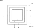
- Fig. 1 is a plan view illustrating a configuration example of a sensor package 100 according to Embodiment 1 of the present disclosure.
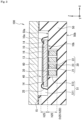
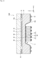
- Fig. 2 is a cross-sectional view illustrating a configuration example of the sensor package 100 according to Embodiment 1 of the present disclosure.
- Fig. 2 illustrates a cross-section of the plan view illustrated in Fig. 1 cut along a line X1-X1' parallel to the X-axis direction.
- the sensor package 100 (an example of a "semiconductor device" according to the present disclosure) includes Peltier effect elements 20, sensor elements 40 (an example of “semiconductor elements” according to the present disclosure), a package substrate 50, wires 25 (an example of "wirings” according to the present disclosure) that connect the sensor elements 40 and the package substrate 50, a seal ring 15 that is provided on an upper surface 50a side of an outer circumference of the package substrate 50, and a sealing glass 60 that is bonded to the package substrate 50 with the seal ring 15 interposed therebetween.
- the package substrate 50, and the seal ring 15 and the sealing glass 60 constitute a package that accommodates and airtightly seals the sensor elements 40 and the Peltier effect elements 20.
- the sensor element 40 is, for example, Complementary Metal Oxide Semiconductor (CMOS) image sensor or a Charge Coupled Device (CCD) image sensor.
- CMOS Complementary Metal Oxide Semiconductor
- CCD Charge Coupled Device
- the sensor element 40 may be referred to as a sensor chip.
- the sensor element 40 includes the semiconductor substrate 10, a color filter layer 13 that is provided on an upper surface 10a side of the semiconductor substrate 10 and in a pixel region, and a microlens layer 16 that is provided on the color filter layer 13.
- the sensor element 40 detects light by photoelectric conversion in the pixel region in which the color filter layer 13 and the microlens layer 16 are disposed.
- the light detected by the sensor element 40 is not limited to visible light, and may be, for example, infrared light or ultraviolet light.
- the semiconductor substrate 10 is, for example, a silicon substrate.
- the semiconductor substrate 10 includes a photoelectric conversion element that is provided in the pixel region, a readout circuit that reads a signal charge generated by the photoelectric conversion element, a signal processing circuit that processes a signal output from the readout circuit, and the like.
- the upper surface 10a (e.g., back surface) side of the semiconductor substrate 10 is provided with an inter-layer insulating film (not illustrated) or the like, and the color filter layer 13 is provided on the inter-layer insulating film. Furthermore, external connection terminals 14 are provided on the upper surface 10a side of the semiconductor substrate 10 and on an outer side of the pixel region.
- a lower surface 10b (e.g., front surface) side of the semiconductor substrate 10 is provided with a rewiring layer 30.
- the rewiring layer 30 is a thin layer formed by a semiconductor process (e.g., Chemical Vapor Deposition (CVD) or spattering).
- the rewiring layer 30 has a structure that thin insulating films and thin wiring layers are alternately laminated, and the wiring layers of the respective layers have inter-layer connection via through holes (vias) or the like.
- the sensor element 40 is provided not on a wiring substrate that has the thickness like, for example, a rigid substrate, but on the lower surface 10b of the semiconductor substrate 10 with the thin rewiring layer 30 formed by the semiconductor process interposed therebetween.
- the external connection terminals 14 are, for example, bonding pads.
- the external connection terminals 14 are connected to the package substrate 50 via the wires 25 such as gold wires.
- the external connection terminals 14 may be connected to the Peltier effect elements 20 via the wirings provided inside the semiconductor substrate 10 and the rewiring layer 30.
- the sensor element 40 includes a pair of the external connection terminals 14.
- the one external connection terminal 14 of the pair of external connection terminals 14 may be used as a positive electrode side terminal that applies a positive potential to the Peltier effect element 20, and the other external connection terminal 14 may be used as a negative electrode side terminal that applies a ground potential or a negative potential to the Peltier effect element 20.
- the voltage is applied between the pair of external connection terminals 14
- the current flows from the one external connection terminal 14 to the other external connection terminal 14 through the Peltier effect element 20.
- Fig. 3 is a plan view illustrating a configuration example of the Peltier effect element 20 according to Embodiment 1 of the present disclosure.
- Fig. 4 is a cross-sectional view illustrating the configuration example of the Peltier effect element 20 according to Embodiment 1 of the present disclosure.
- Fig. 4 illustrates a cross-section of the plan view illustrated in Fig. 3 cut along a line Y1-Y1' parallel to the Y-axis direction.
- the Peltier effect element 20 includes a first electrode 21, a second electrode 22, and a thermoelectric semiconductor 23.
- the first electrode 21 is located between the sensor element 40 and the thermoelectric semiconductor 23, and is connected to the thermoelectric semiconductor 23.
- the second electrode 22 is located on the side opposite to the first electrode 21 with the thermoelectric semiconductor 23 interposed therebetween, and is connected to the thermoelectric semiconductor 23.
- the thermoelectric semiconductor 23 includes a p-type thermoelectric semiconductor 23p and an n-type thermoelectric semiconductor 23n.
- the p-type thermoelectric semiconductor 23p and the n-type thermoelectric semiconductor 23n are alternately aligned and disposed at intervals in one direction.
- the p-type thermoelectric semiconductor 23p and the n-type thermoelectric semiconductor 23n are alternately connected in series via the first electrode 21 and the second electrode 22.
- the first electrode 21 is provided between the rewiring layer 30 and the p-type thermoelectric semiconductor 23p, and between the rewiring layer 30 and the n-type thermoelectric semiconductor 23n.
- the first electrode 21 connects the upper end of the p-type thermoelectric semiconductor 23p and the upper end of the n-type thermoelectric semiconductor 23n.
- the first electrode 21 is made of copper (Cu) or a Cu film formed of a Cu alloy whose main component is Cu, and a conductive adhesive that is coated on the front surface of the Cu film.
- the conductive adhesive is, for example, a solder (e.g., SnAg) or silver (Ag) paste.
- the upper end of the p-type thermoelectric semiconductor 23p and the upper end of the n-type thermoelectric semiconductor 23n are bonded to the first electrode 21 with this conductive adhesive interposed therebetween.
- the second electrode 22 is provided between the package substrate 50 and the p-type thermoelectric semiconductor 23p, and between the package substrate 50 and the n-type thermoelectric semiconductor 23n.
- the second electrode 22 connects the lower end of the p-type thermoelectric semiconductor 23p and the lower end of the n-type thermoelectric semiconductor 23n.
- the second electrode 22 is made of Cu or a Cu film formed of a Cu alloy whose main component is Cu, and a conductive adhesive that is coated on the front surface of the Cu film.
- the conductive adhesive is, for example, a solder (e.g., SnAg) or silver (Ag) paste.
- the lower end of the p-type thermoelectric semiconductor 23p and the lower end of the n-type thermoelectric semiconductor 23n are bonded to the second electrode 22 with this conductive adhesive interposed therebetween.
- the thicknesses of the first electrode 21 and the second electrode 22 are, for example, several ten nanometers or more to several hundred nanometers or less.
- the conductive films that constitute the first electrode 21 and the second electrode 22 are not limited to Cu or the Cu alloy.
- the first electrode 21 and the second electrode 22 may be made of, for example, a single material of titanium (Ti), tungsten (W), titanium nitride (TiN), platinum (Pt), gold (Au), germanium (Ge), palladium (Pd), zinc (Zn), nickel (Ni), or aluminum (Al), or an alloy containing at least one of these materials.
- Each of the first electrode 21 and the second electrode 22 may be a single film of such constituent materials, or may be a laminated film formed by combining two or more types of the constituent materials.
- each of the first electrode 21 and the second electrode 22 may be made of a laminated film of titanium and tungsten.
- the semiconductor substrate 10 absorbs heat T1 (performs heat absorption), and the package substrate 50 discharges heat T2 (performs heat discharge).
- the Peltier effect element 20 enables heat produced in the sensor element 40 to escape to the outside of the sensor package 100 through the package substrate 50.
- the package substrate 50 illustrated in Fig. 2 is a multilayer substrate formed by laminating an insulation layer and a wiring layer, and is, for example, a ceramic substrate made of alumina (or aluminum oxide) or the like, or an organic substrate made of epoxy glass.
- the package substrate 50 is, for example, a Pin Grid Array (PGA) substrate, may be a Ball Grid Array (BGA), or may be a Land Grid Array (LGA).
- An interior located between the upper surface 50a and a bottom surface 50b of the package substrate 50 is provided with multiple layers of a plurality of wirings. These wirings connect a plurality of terminals (not illustrated; e.g., solder balls) provided in the bottom surface 50b of the package substrate 50.
- the upper surface 50a side of the package substrate 50 is provided with a cavity 51.
- the cavity 51 includes an upper recess 511 and a lower recess 512 (an example of a "first recess" according to the present disclosure) provided on a bottom surface side of the upper recess 511.
- the shapes of the upper recess 511 and the lower recess 512 in plan view are, for example, rectangular shapes.
- the diameter of the opening plane of the upper recess 511 is greater than that of the lower recess 512.
- the sensor elements 40 are disposed in the upper recess 511, and the Peltier effect elements 20 are disposed in the lower recess 512.
- the second electrodes 22 (see Fig. 4 ) of the Peltier effect elements 20 are provided on the bottom surface of the lower recess 512.
- the depth of the lower recess 512 is the same as or is substantially the same as heights (e.g., a height from the upper end of the first electrode 21 to the lower end of the second electrode 22) h20 of the Peltier effect elements 20 disposed in the lower recess 512.
- substantially all the Peltier effect elements 20 are disposed in the lower recess 512.
- loop heights h25 of the wires 25 are lower than the heights h20 of the Peltier effect elements 20 (h25 ⁇ h20).
- the wire 25 has a smaller diameter and cross-sectional area than those of wires (not illustrated) provided inside the package substrate 50, and therefore has a high wiring resistance and inductance.
- h25 ⁇ h20 as described above, it is possible to reduce the wiring resistance and the inductance of the wires 25.
- the wirings e.g., a power supply wiring, a reference potential (e.g., ground potential GND) wiring, and a signal wiring
- the wirings e.g., a power supply wiring, a reference potential (e.g., ground potential GND) wiring, and a signal wiring
- a resin having the insulation property may be filled between the sensor elements 40 and the bottom surface of the lower recess 512.
- a resin having the insulation property may be filled between the sensor elements 40 and the bottom surface of the lower recess 512.
- a manufacturing method for the sensor package 100 illustrated in Figs. 1 and 2 will be described.
- various devices such as a device that manufactures a wafer (hereinafter, sensor wafer) 10' on which the sensor elements 40 have been multiply imposed and formed, a device that dices the sensor wafer, a device that attaches the thermoelectric semiconductor 23 to the first electrode 21 and the second electrode 22, and a wire bonding device are used.
- these devices will be collectively referred to as a manufacturing device in the embodiments of the present disclosure.
- at least part of work performed by the manufacturing device may be performed by a worker.
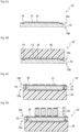
- Figs. 5A to 5F are cross-sectional views illustrating the manufacturing method for the sensor package 100 according to Embodiment 1 of the present disclosure.
- the manufacturing device manufactures the sensor wafer 10'.
- the sensor wafer 10' is the semiconductor substrate 10 on which the sensor elements 40 have been multiply imposed and formed and that is not yet diced.
- the color filter layer 13 and the microlens layer 16 are attached to the upper surface 10a side of the semiconductor substrate 10.
- the rewiring layer 30 and the first electrodes 21 are not yet formed.
- the rewiring layer 30 and the first electrodes 21 are formed by a process in Fig. 5C described later.
- the manufacturing device bonds the support substrate 26 on the upper surface 10a side of the semiconductor substrate 10.
- the support substrate 26 protects the upper surface 10a side of the semiconductor substrate 10 including the color filter layer 13 and the microlens layer 16.
- the manufacturing device turns the semiconductor substrate 10 upside down such that the lower surface 10b side of the semiconductor substrate 10 faces upward. In this state, the manufacturing device forms the rewiring layer 30 on the lower surface 10b side of the semiconductor substrate 10.
- the manufacturing device forms through holes (vias) H1 that penetrate between the lower surface 10b and the upper surface 10a of the semiconductor substrate 10 from the lower surface 10b side of the semiconductor substrate 10. Furthermore, the manufacturing device forms through electrodes 27 inside the through holes H1. The through electrodes 27 and the rewiring layer 30 lead part of the wirings included in the sensor elements 40 to the lower surface 10b side.
- the manufacturing device forms the first electrodes 21 of the Peltier effect elements 20 (see Fig. 2 ) on the lower surface 10b side of the semiconductor substrate 10.
- the manufacturing device forms the copper (Cu) film on the lower surface 10b side of the semiconductor substrate 10 using a deposition method, a spattering method, or a CVD method.
- the manufacturing device forms a resist pattern of a predetermined shape on the Cu film using photolithography.
- the manufacturing device etches the Cu film using the resist pattern as a mask.
- the manufacturing device forms the first electrodes 21 from the Cu film.
- the manufacturing device may form the first electrodes 21 from the Cu film using a lift-off method.
- the manufacturing device may form the first electrodes 21 by an arbitrary method.
- the manufacturing device attaches the p-type thermoelectric semiconductors 23p and the n-type thermoelectric semiconductors 23n on the first electrodes 21.
- the manufacturing device presses against the lower surface 10b side of the semiconductor substrate 10 a sheet to which the p-type thermoelectric semiconductors 23p and the n-type thermoelectric semiconductors 23n are adhered in advance, solders and connects the p-type thermoelectric semiconductors 23p and the n-type thermoelectric semiconductors 23n to the first electrodes 21, then removes only the sheet, and thereby attaches the p-type thermoelectric semiconductors 23p and the n-type thermoelectric semiconductors 23n on the first electrodes 21.
- the p-type thermoelectric semiconductors 23p and the n-type thermoelectric semiconductors 23n may be attached on the first electrode 21 by other methods.
- the p-type thermoelectric semiconductor 23p and the n-type thermoelectric semiconductor 23n may be attached one by one on the first electrode 21.
- the manufacturing device dices (not illustrated) and singulates the sensor wafer 10' and the support substrate 26. Subsequently, the manufacturing device detaches the support substrate 26 from the upper surface 10a side of the semiconductor substrate 10.
- the manufacturing device disposes in the cavity 51 of the package substrate 50 the semiconductor substrate 10 to which the p-type thermoelectric semiconductors 23p and the n-type thermoelectric semiconductors 23n have been attached, and mounts the lower surface 10b side of the semiconductor substrate 10 on the bottom surface of the cavity 51 by solder connection.
- electrodes of the rewiring layer 30 provided to the semiconductor substrate 10 are soldered and connected to the bottom surface of the upper recess 511, and the p-type thermoelectric semiconductors 23p and the n-type thermoelectric semiconductors 23n are soldered and connected to the bottom surface of the lower recess 512 with the second electrodes 22 interposed therebetween.
- the second electrodes 22 are provided in advance to the lower ends of the p-type thermoelectric semiconductors 23p and the n-type thermoelectric semiconductor 23n.
- solder connection fixes the positions of the semiconductor substrate 10 and the Peltier effect elements 20 in the cavity 51.
- a conductive material used for this connection is not limited to a solder, and may be a material (e.g., Ag paste) other than the solder.
- the manufacturing device connects the external connection terminals 14 of the sensor elements 40 and the bonding pads (not illustrated) of the package substrate 50 by the wires 25. Subsequently, the manufacturing device attaches the sealing glass 60 (see Fig. 2 ) to the package substrate 50 by means such as the seal ring 15 (see Fig. 2 ) or a thermosetting adhesive in a state where the positions of the sealing glass 60 and the package substrate 50 are adjusted. Consequently, a space (i.e., cavity 51) between the sealing glass 60 and the package substrate 50 is sealed airtightly.
- the sensor package 100 illustrated in Figs. 1 and 2 is finished.
- the second electrodes 22 may be provided in advance on the bottom surface of the lower recess 512 of the package substrate 50 instead of the lower ends of the p-type thermoelectric semiconductors 23p and the n-type thermoelectric semiconductors 23n.
- the lower ends of the p-type thermoelectric semiconductors 23p and the n-type thermoelectric semiconductors 23n are bonded to the second electrodes 22 provided in advance on the bottom surface of the lower recess 512.
- a conductive adhesive such as a solder or Ag paste may be used.
- Such a method can also manufacture the sensor package 100 illustrated in Figs. 1 and 2 .
- Fig. 6 is a cross-sectional view illustrating a configuration example of a semiconductor device 200 according to Embodiment 1 of the present disclosure.
- the semiconductor device 200 includes the sensor package 100 and a motherboard 150.
- the motherboard 150 is a multilayer substrate formed by laminating an insulation layer and a wiring layer, and is, for example, a ceramic substrate made of alumina (aluminum oxide) or the like or an organic substrate made of epoxy glass.
- the sensor package 100 is mounted on a front surface 150a of the motherboard 150.
- the sensor elements 40 and the Peltier effect elements 20 included in the sensor package 100 are connected to wirings of the motherboard 150 via a plurality of terminals 70 provided in the bottom surface 50b of the package substrate 50.
- the plurality of terminals 70 may be, for example, ball-shaped terminals (e.g., solder balls), may be planar terminals, or may be pin-shaped terminals. In a case where the plurality of terminals 70 are the planar terminals or the pin-shaped terminals, the sensor package 100 may be attached to the motherboard 150 via a socket (not illustrated).
- ball-shaped terminals e.g., solder balls
- the sensor package 100 may be attached to the motherboard 150 via a socket (not illustrated).
- the sensor package 100 includes the sensor elements 40, the Peltier effect elements 20 that are attached to the lower surface 10b of the sensor elements 40 without the wiring substrate, and the package substrate 50 to which the sensor elements 40 are attached.
- a region of the package substrate 50 that faces the lower surface 10b of the sensor elements 40 is provided with the lower recess 512.
- the Peltier effect elements 20 are disposed in the lower recess 512.
- the Peltier effect elements 20 are accommodated in the lower recess 512, so that it is easy to secure the heights of the Peltier effect elements 20. It is possible to increase a distance between the lower surface 10b of the sensor elements 40 that are the heat absorption side and the bottom surface of the lower recess 512 of the package substrate 50 that is a heat discharge side, and suppress heat transfer from the heat discharge side to the heat discharge side. Consequently, it is possible to improve the cooling efficiency of the Peltier effect elements 20 of cooling the sensor elements 40.
- the Peltier effect elements 20 are accommodated in the lower recess 512, so that it is possible to reduce the height of the sensor package 100 compared to a case where there is no lower recess 512. Consequently, it is possible to achieve both of improvement of the cooling efficiency for the sensor elements 40 and reduction of the height of the sensor package 100.
- the loop heights h25 of the wires 25 are lower than the heights h20 of the Peltier effect elements 20 (h25 ⁇ h20). Consequently, it is possible to reduce the wiring resistance and the inductance of the wirings (e.g., the power supply wiring, the GND wiring, and the signal wiring) including the wires 25 among the wires included in the sensor elements 40, so that it is possible to improve the electrical characteristics of the sensor elements 40.
- the wirings e.g., the power supply wiring, the GND wiring, and the signal wiring
- Embodiment 1 has described that the Peltier effect elements 20 are disposed in the lower recess 512 of the package substrate 50.
- the region in which the Peltier effect elements 20 are disposed is not limited to a recess.
- the region in which the Peltier effect elements 20 are disposed may be a through hole.
- Fig. 7 is a cross-sectional view illustrating a configuration example of a sensor package 100A according to Embodiment 2 of the present disclosure.
- the package substrate 50 included in the sensor package 100A (the example of the "semiconductor device" according to the present disclosure) includes a cavity 51A.
- the cavity 51A includes the upper recess 511 and through holes 512A provided in the bottom surface of the upper recess 511.
- the Peltier effect elements 20 are disposed in the through holes 512A of the cavity 51A.
- the lower ends of the Peltier effect elements 20 e.g., the lower ends of the second electrodes 22
- the second electrodes 22 may be, for example, the ball-shaped terminals, may be the planar terminals, or may be the pin-shaped terminals.
- Fig. 7 illustrates a case where the second electrodes 22 are the planar terminals.
- an adhesive 18 is disposed between the lower surface 10b of the semiconductor substrate 10 and the bottom surface of the upper recess 511 of the cavity 51.
- the adhesive 18 fixes the semiconductor substrate 10 to the package substrate 50.
- Fig. 8 is a cross-sectional view illustrating a configuration example of a semiconductor device 200A according to Embodiment 2 of the present disclosure.
- the semiconductor device 200A includes the sensor package 100A and the motherboard 150.
- the sensor package 100A is mounted on the front surface 150a of the motherboard 150.
- the sensor elements 40 are connected to the wirings of the motherboard 150 via the plurality of terminals 70 provided in the bottom surface 50b of the package substrate 50.
- the Peltier effect elements 20 are connected to the wirings of the motherboard 150 via the second electrodes 22.
- the plurality of terminals 70 and the second electrodes 22 are connected to the wirings or the like using the conductive adhesive such as the solder or Ag paste.
- the second electrodes 22 of the Peltier effect elements 20 may be provided in advance on the front surface 150a of the motherboard 150 instead of the lower ends of the p-type thermoelectric semiconductors 23p and the n-type thermoelectric semiconductors 23n.
- the second electrodes 22 may be provided in advance on the front surface 150a as part of the wirings of the motherboard 150.
- the sensor package 100A includes the sensor elements 40, the Peltier effect elements 20 that are attached to the lower surface 10b of the sensor elements 40 without the wiring substrate, and the package substrate 50 to which the sensor elements 40 are attached.
- the region of the package substrate 50 that faces the lower surface 10b of the sensor elements 40 is provided with the through holes 512A.
- the Peltier effect elements 20 are disposed in the through holes 512A.
- Embodiment 2 provides the same effect as that of Embodiment 1. That is, the Peltier effect elements 20 are accommodated in the through hole 512A, so that it is easy to secure the heights of the Peltier effect elements 20. Consequently, it is possible to improve the cooling efficiency of the Peltier effect elements 20 of cooling the sensor elements 40.
- the Peltier effect elements 20 are accommodated in the through holes 512A, so that it is possible to reduce the height of the sensor package 100. It is possible to achieve both of improvement of the cooling efficiency for the sensor elements 40 and reduction of the height of the sensor package 100.
- the loop heights h25 of the wires 25 are lower than the heights h20 of the Peltier effect elements 20 (h25 ⁇ h20). Consequently, it is possible to reduce the wiring resistance and the inductance of the wirings (e.g., the power supply wiring, the GND wiring, and the signal wiring) including the wires 25, so that it is possible to improve the electrical characteristics of the sensor elements 40.
- the wirings e.g., the power supply wiring, the GND wiring, and the signal wiring
- Embodiment 2 has described that the lower ends of the Peltier effect elements 20 disposed in the through holes 512A of the cavity 51 and the bottom surface 50b of the package substrate 50 match or substantially match in the Z-axis direction.
- the Peltier effect elements 20 may protrude from the bottom surface 50b of the package substrate 50.
- Fig. 9 is a cross-sectional view illustrating a configuration example of a sensor package 100B according to Embodiment 3 of the present disclosure.
- the sensor package 100B the example of the "semiconductor device" according to the present disclosure
- the lower portions of the thermoelectric semiconductors 23 and the second electrodes 22 of the Peltier effect elements 20 protrude from the bottom surface 50b of the package substrate 50.
- the second electrodes 22 may be, for example, the ball-shaped terminals, may be the planar terminals, or may be the pin-shaped terminals.
- Fig. 9 illustrates a case where the second electrodes 22 are the planar terminals.
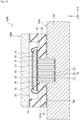
- Fig. 10 is a cross-sectional view illustrating a configuration example of a semiconductor device 200B according to Embodiment 3 of the present disclosure.
- the semiconductor device 200B (the example of the "semiconductor device" according to the present disclosure) includes the sensor package 100B, and the motherboard 150.
- the sensor package 100B is mounted on the front surface 150a of the motherboard 150.
- a front surface 150a side of the motherboard 150 is provided with a recess 151 (an example of a "third recess" according to the present disclosure).
- the lower portions and the second electrodes 22 of the Peltier effect elements 20 protruding from the bottom surface 50b of the package substrate 50 are disposed in the recess 151 of the motherboard 150.
- the second electrodes 22 of the Peltier effect elements 20 are connected to wirings or the like provided in the bottom surface of the recess 151 of the motherboard 150.
- the second electrodes 22 are connected to the wirings or the like using the conductive adhesive such as the solder or Ag paste.
- the semiconductor device 200B includes the sensor package 100B, and the motherboard 150 to which the package substrate 50 of the sensor package 100B is attached.
- the motherboard 150 is provided with the recess 151 that faces the through holes 512A of the package substrate 50.
- the Peltier effect elements 20 are disposed in the through holes 512A and the recess 151.
- Embodiment 3 provides the same effect as that of Embodiments 1 and 2. That is, the Peltier effect elements 20 are accommodated in the through holes 512A of the package substrate 50 and the recess 151 of the motherboard 150, so that it is easy to secure the heights of the Peltier effect elements 20. Consequently, it is possible to improve the cooling efficiency of the Peltier effect elements 20 of cooling the sensor elements 40.
- the Peltier effect elements 20 are accommodated in the through holes 512A of the package substrate 50 and the recess 151 of the motherboard 150, so that it is possible to reduce the height of the semiconductor device 200B including the sensor package 100B. It is possible to achieve both of improvement of the cooling efficiency for the sensor elements 40 and reduction of the height of the semiconductor device 200B.
- the sensor packages 100, 100A, and 100B include the package substrate 50.
- the configuration of the sensor package is not limited thereto.
- the package format of the sensor package may employ a configuration from which the package substrate 50 is omitted, and may be, for example, a Wafer Level Chip Size Package (WLCSP).
- WLCSP Wafer Level Chip Size Package
- Fig. 11 is a cross-sectional view illustrating a configuration example of a sensor package 100C according to Embodiment 4 of the present disclosure.
- the package format of the sensor package 100C is, for example, a WLCSP.
- the WLCSP is, for example, a package formed by exposing part of a semiconductor substrate (a diced wafer) without performing wiring using bonding wires.
- the WLCSP is a package formed by substantially reducing the size of the Ball Grid Array (BGA) to the same size as that of a sensor chip. It is possible to provide an effect of reduction of the weight, the thickness, and the length of electronic devices such as digital cameras and mobile telephones.
- BGA Ball Grid Array
- the lower surface 10b side of the semiconductor substrate 10 is provided with external connection terminals 19 of the WLCSP and the Peltier effect elements 20 with the rewiring layer 30 interposed therebetween.
- FIG. 11 illustrates a case where the external connection terminals 19 and the second electrodes 22 of the Peltier effect elements 20 are the ball-shaped terminals (e.g., solder balls), this case is merely an example.
- the external connection terminals 19 of the WLCSP and the second electrodes 22 of the Peltier effect elements 20 may be the planar terminals.
- Fig. 12 is a cross-sectional view illustrating a configuration example of a semiconductor device 200C according to Embodiment 4 of the present disclosure.
- the semiconductor device 200C (the example of the "semiconductor device" according to the present disclosure) includes the sensor package 100C whose package format is the WLCSP, and the motherboard 150.
- the sensor package 100C is mounted on the front surface 150a of the motherboard 150.
- the front surface 150a side of the motherboard 150 is provided with the recess 151.
- the Peltier effect elements 20 provided on a lower surface side of the sensor package 100C are disposed in the recess 151 of the motherboard 150.
- the second electrodes 22 of the Peltier effect elements 20 are connected to the wirings or the like provided in the bottom surface of the recess 151 of the motherboard 150.
- the second electrodes 22 are connected to the wirings or the like using the conductive adhesive such as the solder or Ag paste.
- the external connection terminals 19 of a sensor package 100D are connected to wirings or the like provided on the front surface 150a side of the motherboard 150 and in a region other than the recess 151.
- Embodiment 4 provides the same effect as that of Embodiments 1 to 3. That is, the Peltier effect elements 20 are accommodated in the recess 151 of the motherboard 150, so that it is easy to secure the heights of the Peltier effect elements 20. Consequently, it is possible to improve the cooling efficiency for the sensor elements 40.
- the Peltier effect elements 20 are accommodated in the recess 151 of the motherboard 150, so that it is possible to reduce the height of the semiconductor device 200C. It is possible to achieve both of improvement of the cooling efficiency for the sensor elements 40 and reduction of the height of the semiconductor device 200C.
- the package format of the sensor package 100C is, for example, a WLCSP. Consequently, it is possible to narrow pitches of the power supply terminal, the GND terminal, and the signal terminal of the sensor package 100C (miniaturize the package).
- Fig. 13 is a cross-sectional view illustrating a configuration example of a sensor package 100D according to Embodiment 5 of the present disclosure.
- a difference of the sensor package 100D (the example of the "semiconductor device" according to the present disclosure) illustrated in Fig. 13 from the sensor package 100C illustrated in Fig. 11 is that a recess 11 (an example of a "second recess” according to the present disclosure) is provided on the lower surface 10b side of the semiconductor substrate 10.
- the Peltier effect elements 20 are disposed in the recess 11.
- Fig. 14 is a cross-sectional view illustrating a configuration example of a semiconductor device 200D according to Embodiment 5 of the present disclosure.
- the semiconductor device 200D includes the sensor package 100D and the motherboard 150.
- the sensor package 100D is mounted on the front surface 150a of the motherboard 150.
- the external connection terminals 19 of the sensor package 100D and the second electrodes 22 of the Peltier effect elements 20 are connected to the wirings or the like provided on the front surface 150a side of the motherboard 150.
- the external connection terminals 19 and the second electrodes 22 are connected to the wirings or the like using the conductive adhesive such as the solder or Ag paste.
- the sensor package 100D according to Embodiment 5 of the present disclosure includes the sensor elements 40, and the Peltier effect elements 20 that are attached to the lower surface 10b of the sensor elements 40 without the wiring substrate.
- the recess 11 is provided in the lower surface 10b of sensor elements 40.
- the Peltier effect elements 20 are disposed in the recess 11.
- Embodiment 5 provides the same effect as that of Embodiments 1 to 4. That is, the Peltier effect elements 20 are accommodated in the recess 11 of the sensor elements 40, so that it is easy to secure the heights of the Peltier effect elements 20. Consequently, it is possible to improve the cooling efficiency for the sensor elements 40.
- the Peltier effect elements 20 are accommodated in the recess 11 of the sensor elements 40, so that it is possible to reduce the height of the sensor package 100D. It is possible to achieve both of improvement of the cooling efficiency for the sensor elements 40 and reduction of the height of the sensor package 100D.
- the package format of the semiconductor device 200D is, for example, the WLCSP. Consequently, it is possible to narrow pitches of the power supply terminal, the GND terminal, and the signal terminal of the sensor package 100D (miniaturize the package).
- Fig. 15 is a cross-sectional view illustrating a configuration example of a sensor package 100E according to Embodiment 6 of the present disclosure.
- a difference of the sensor package 100E (the example of the "semiconductor device" according to the present disclosure) illustrated in Fig. 15 from the sensor package 100D illustrated in Fig. 13 is that part of the Peltier effect elements 20 protrude from the lower surface 10b of the semiconductor substrate 10.
- Fig. 15 illustrates a case where the second electrodes 22 are the ball-shaped terminals (e.g., solder balls).
- the second electrodes 22 are not limited to the ball-shaped terminals, and may be, for example, the planar terminals.
- Fig. 16 is a cross-sectional view illustrating a configuration example of a semiconductor device 200E according to Embodiment 6 of the present disclosure.
- the semiconductor device 200E (the example of the "semiconductor device" according to the present disclosure) includes the sensor package 100E and the motherboard 150.
- the sensor package 100E is mounted on the front surface 150a of the motherboard 150.
- the front surface 150a side of the motherboard 150 is provided with the recess 151.
- the lower portions of the Peltier effect elements 20 and the second electrodes 22 protruding from the lower surface 10b of the semiconductor substrate 10 are disposed in the recess 151 of the motherboard 150.
- the second electrodes 22 of the Peltier effect elements 20 are connected to the wirings or the like provided in the bottom surface of the recess 151 of the motherboard 150.
- the second electrodes 22 are connected to the wirings or the like using the conductive adhesive such as the solder or Ag paste.
- the semiconductor device 200E includes the sensor package 100E, and the motherboard 150 to which the sensor package 100E is attached.
- the motherboard 150 is provided with the recess 151 that faces the recess 11 of the lower surface 10b of the sensor elements 40.
- the Peltier effect elements 20 are disposed in the recess 11 and in the recess 151.
- Embodiment 6 provides the same effect as that of Embodiments 1 to 5.
- the Peltier effect elements 20 are accommodated in the recess 11 and in the recess 151, so that it is easy to secure the heights of the Peltier effect elements 20. Consequently, it is possible to improve the cooling efficiency of the Peltier effect elements 20 of cooling the sensor elements 40.
- the Peltier effect elements 20 are disposed in the recess 11 and in the recess 151, so that it is possible to reduce the height of the semiconductor device 200E including the sensor package 100E. It is possible to achieve both of improvement of the cooling efficiency for the sensor elements 40 and reduction of the height of the semiconductor device 200E.
- the semiconductor elements according to the present disclosure are not limited to the semiconductor elements.
- the semiconductor elements according to the present disclosure may be, for example, various IC elements such as Large Scale Integrated (LSI) circuits or memory elements.
- LSI Large Scale Integrated
- Fig. 17 is a cross-sectional view illustrating a configuration example of an IC element 140 according to Embodiment 7 of the present disclosure.
- the IC element 140 illustrated in Fig. 17 is, for example, an LSI element, and a package format thereof is the WLCSP.
- the lower surface 10b side of the semiconductor substrate 10 is provided with the external connection terminals 19 of the WLCSP and the Peltier effect elements 20 with the rewiring layer 30 interposed therebetween.
- FIG. 17 illustrates a case where the external connection terminals 19 and the second electrodes 22 of the Peltier effect elements 20 are the ball-shaped terminals (e.g., solder balls), this case is merely an example.
- the external connection terminals 19 of the WLCSP and the second electrodes 22 of the Peltier effect elements 20 may be the planar terminals.
- Fig. 18 is a cross-sectional view illustrating a configuration example of a semiconductor device 200F according to Embodiment 7 of the present disclosure.
- the semiconductor device 200F (the example of the "semiconductor device" according to the present disclosure) includes the IC element 140 and the motherboard 150.
- the IC element 140 is mounted on the front surface 150a of the motherboard 150.
- the front surface 150a side of the motherboard 150 is provided with the recess 151.
- the Peltier effect elements 20 provided on the lower surface 10b side of the IC element 140 are disposed in the recess 151 of the motherboard 150.
- the second electrodes 22 of the Peltier effect elements 20 are connected to the wirings or the like provided in the bottom surface of the recess 151 of the motherboard 150.
- the second electrodes 22 are connected to the wirings or the like using the conductive adhesive such as the solder or Ag paste.
- the external connection terminals 19 of the IC element 140 are connected to wirings or the like provided on the front surface 150a side of the motherboard 150 and in a region other than the recess 151.
- the semiconductor device 200F includes the IC element 140, the Peltier effect elements 20 that are attached to the lower surface 10b of the IC elements 140 without the wiring substrate, and the motherboard 150 that faces the IC element 140 with the Peltier effect elements 20 interposed therebetween.
- the motherboard 150 is provided with the recess 151.
- the Peltier effect elements 20 are disposed in the recess 151.
- Embodiment 7 provides the same effect as that of Embodiments 1 to 6.
- the Peltier effect elements 20 are accommodated in the recess 151 of the motherboard 150, so that it is easy to secure the heights of the Peltier effect elements 20. Consequently, it is possible to improve the cooling efficiency for the IC element 140.
- the Peltier effect elements 20 are accommodated in the recess 151 of the motherboard 150, so that it is possible to reduce the height of the semiconductor device 200F. It is possible to achieve both of improvement of the cooling efficiency for the IC element 140 and reduction of the height of the semiconductor device 200F.
- the IC element 140 is the WLCSP. Consequently, it is possible to narrow pitches of the power supply terminal, the GND terminal, and the signal terminal of the IC element 140 (miniaturize the package).
- Embodiment 7 has described a case where the IC element 140 is mounted on the motherboard in a bare state.
- the IC element 140 may be sealed with a resin.
- Fig. 19 is a cross-sectional view illustrating a configuration example of an IC package 100G according to Embodiment 8 of the present disclosure.
- the IC package 100G includes the IC element 140, and a sealing resin 90 that seals the upper surface 10a (e.g., back surface) and the side surfaces of the IC element 140.
- a package format of the IC package 100G is, for example, a Fan Out Wafer Level Package (FOWLP) or a Fan Out Panel Level Package (FOPLP).
- a material of the sealing resin 90 is an epoxy resin, a phenol resin, or the like.
- the lower surface 10b (e.g., front surface) side of the semiconductor substrate 10 is provided with the external connection terminals 19 of the IC package 100G and the Peltier effect elements 20 with the rewiring layer 30 interposed therebetween.
- FIG. 19 illustrates a case where the external connection terminals 19 and the second electrodes 22 of the Peltier effect elements 20 are the ball-shaped terminals (e.g., solder balls), this case is merely an example.
- the external connection terminals 19 and the second electrodes 22 of the Peltier effect elements 20 may be the planar terminals.
- Fig. 20 is a cross-sectional view illustrating a configuration example of a semiconductor device 200G according to Embodiment 8 of the present disclosure.
- the semiconductor device 200F (the example of the "semiconductor device" according to the present disclosure) includes the IC package 100G whose package format is the FOWLP or the FOPLP, and the motherboard 150.
- the IC package 100G is mounted on the front surface 150a of the motherboard 150.
- the front surface 150a side of the motherboard 150 is provided with the recess 151.
- the Peltier effect elements 20 provided on a lower surface side of the IC package 100G are disposed in the recess 151 of the motherboard 150.
- the second electrodes 22 of the Peltier effect elements 20 are connected to the wirings or the like provided in the bottom surface of the recess 151 of the motherboard 150.
- the second electrodes 22 are connected to the wirings or the like using the conductive adhesive such as the solder or Ag paste.
- the external connection terminals 19 of the IC package 100G are connected to wirings or the like provided on the front surface 150a side of the motherboard 150 and in a region other than the recess 151.
- Embodiment 8 provides the same effect as that of Embodiments 1 to 7. That is, the Peltier effect elements 20 are accommodated in the recess 151 of the motherboard 150, so that it is easy to secure the heights of the Peltier effect elements 20. Consequently, it is possible to improve the cooling efficiency for the IC element 140.
- the Peltier effect elements 20 are accommodated in the recess 151 of the motherboard 150, so that it is possible to reduce the height of the semiconductor device 200G. It is possible to achieve both of improvement of the cooling efficiency for the IC element 140 and reduction of the height of the semiconductor device 200G.
- the package format of the IC package 100G is, a FOWLP or a FOPLP. Consequently, it is possible to narrow pitches of the power supply terminal, the GND terminal, and the signal terminal of the IC package 100G (miniaturize the package).
- Fig. 21 is a block diagram illustrating a schematic configuration example of an imaging system according to Embodiment 9 of the present disclosure.
- an imaging system 1000 according to Embodiment 9 of the present disclosure includes a sensor package 1100, a Field-Programmable Gate Array (FPGA) 1200, and a temperature controller 1300.
- FPGA Field-Programmable Gate Array
- the FPGA 1200 is, for example, a control device for controlling the sensor package 1100.
- the FPGA 1200 inputs a control signal for controlling the sensor package 1100 to the sensor package 1100 via the pin-shaped terminal or the like.
- an Inter-Integrated Circuit (I2C) As an interface that connects the FPGA 1200 and the sensor package 1100, an Inter-Integrated Circuit (I2C), a Serial Peripheral Interface (SPI), or the like can be used.
- I2C Inter-Integrated Circuit
- SPI Serial Peripheral Interface
- an information processing device such as an Image Signal Processor (ISP) may be used instead of the FPGA 1200.
- ISP Image Signal Processor
- the sensor package 1100 includes, for example, a thermometer circuit 120 and an AD conversion circuit 121. Temperature data (detection result) detected by the thermometer circuit 120 and converted into a digital value by the AD conversion circuit 121 is output to the FPGA 1200 via, for example, the same interface as an interface such as the I2C or the SPI that connects the FPGA 1200 and the sensor package 1100.
- a dedicated line or a dedicated terminal for outputting the temperature data to an outside of the sensor package can be omitted.
- the temperature controller 1300 controls the Peltier effect elements 20 according to, for example, a control signal from the FPGA 1200. More specifically, the temperature controller 1300 forms a current waveform to be given to the Peltier effect elements 20 according to the control signal from the FPGA 1200, and supplies the current waveform to the Peltier effect elements 20 via the pin-shaped terminals or the like.
- thermometer circuit 120 is disposed inside the sensor package 1100, so that it is possible to directly measure the temperature of the sensor package 1100 itself. Consequently, it is possible to enhance accuracy of the measured sensor chip temperature.
- thermometer circuit 120 an analog value output from the thermometer circuit 120 is converted into a digital value by the AD conversion circuit 121 in the sensor package 1100, so that it is possible to reduce an influence of noise of the measurement result detected by the thermometer circuit 120. Consequently, it is possible to enhance robustness of the measured temperature.
- a measurement result By converting a measurement result into a digital value, it is possible to output a measurement result to the outside of the sensor package using a control signal of the I2C, the SPI, or the like. It is not necessary to provide a dedicated terminal for outputting the measurement result to the outside of the sensor package. Consequently, it is possible to output the measurement result to the outside without restriction of the number of terminals on the sensor package.
- a separate part is not attached to the sensor package 1100 unlike a discrete thermistor element, so that it is also possible to suppress a decrease in a yield rate due to a failure of the thermistor element, an attachment failure, or the like.
- the technology of the present disclosure can be applied to various products.
- the technique according to the present disclosure may be realized as a device mounted on any type of moving body such as an automobile, an electric automobile, a hybrid electric automobile, a motorcycle, a bicycle, a personal mobility device, an airplane, a drone, a ship, a robot, or the like.
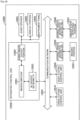
- Fig. 22 is a block diagram illustrating a schematic configuration example of a vehicle control system, which is an example of a moving body control system to which the technique according to the present disclosure can be applied.
- the vehicle control system 12000 includes a plurality of electronic control units connected thereto via a communication network 12001.
- the vehicle control system 12000 includes a drive system control unit 12010, a body system control unit 12020, an external vehicle information detecting unit 12030, an internal vehicle information detecting unit 12040, and an integrated control unit 12050.
- a microcomputer 12051, an audio/image output portion 12052, and an in-vehicle network interface (I/F) 12053 are illustrated as a functional configuration of the integrated control unit 12050.
- the drive system control unit 12010 controls an operation of an apparatus related to a drive system of a vehicle according to various programs.
- the drive system control unit 12010 functions as a driving force generator for generating a driving force of a vehicle such as an internal combustion engine or a driving motor, a driving force transmission mechanism for transmitting a driving force to wheels, a steering mechanism for adjusting a turning angle of a vehicle, and a control apparatus such as a braking apparatus that generates a braking force of a vehicle.
- the body system control unit 12020 controls operations of various devices mounted in the vehicle body according to various programs.
- the body system control unit 12020 functions as a control device of a keyless entry system, a smart key system, a power window device, or various lamps such as a headlamp, a back lamp, a brake lamp, a turn signal, and a fog lamp.
- radio waves transmitted from a portable device that substitutes for a key or signals of various switches may be input to the body system control unit 12020.
- the body system control unit 12020 receives inputs of the radio waves or signals and controls a door lock device, a power window device, and a lamp of the vehicle.
- the external vehicle information detecting unit 12030 detects information on the outside of the vehicle having the vehicle control system 12000 mounted thereon.
- an imaging portion 12031 is connected to the external vehicle information detecting unit 12030.
- the external vehicle information detecting unit 12030 causes the imaging portion 12031 to capture an image of the outside of the vehicle and receives the captured image.
- the external vehicle information detecting unit 12030 may perform object detection processing or distance detection processing for peoples, cars, obstacles, signs, and letters on the road on the basis of the received image.
- the imaging portion 12031 is an optical sensor that receives light and outputs an electrical signal according to the amount of the received light.
- the imaging portion 12031 can also output the electrical signal as an image or distance measurement information.
- the light received by the imaging portion 12031 may be visible light or invisible light such as infrared light.
- the internal vehicle information detecting unit 12040 detects information on the inside of the vehicle.
- a driver state detecting unit 12041 that detects a driver's state is connected to the internal vehicle information detecting unit 12040.
- the driver state detecting unit 12041 includes, for example, a camera that captures an image of a driver, and the internal vehicle information detecting unit 12040 may calculate a degree of fatigue or concentration of the driver or may determine whether or not the driver is dozing on the basis of detection information input from the driver state detecting unit 12041.
- the microcomputer 12051 can calculate a control target value of the driving force generation device, the steering mechanism, or the braking device on the basis of the information on the outside or the inside of the vehicle acquired by the external vehicle information detecting unit 12030 or the internal vehicle information detecting unit 12040 and output a control command to the drive system control unit 12010.
- the microcomputer 12051 can perform cooperative control for the purpose of obtaining functions of an Advanced Driver Assistance System (ADAS) including collision avoidance or impact mitigation of a vehicle, following traveling based on inter-vehicle distance, vehicle speed maintenance driving, vehicle collision warning, vehicle lane deviation warning, or the like.
- ADAS Advanced Driver Assistance System
- the microcomputer 12051 can perform cooperative control for the purpose of automated driving or the like in which autonomous travel is performed without depending on operations of the driver, by controlling the driving force generator, the steering mechanism, or the braking device and the like on the basis of information about the surroundings of the vehicle, the information being acquired by the external vehicle information detecting unit 12030 or the internal vehicle information detecting unit 12040.
- the microcomputer 12051 can output a control command to the body system control unit 12020 based on the information acquired by the external vehicle information detecting unit 12030 outside the vehicle.
- the microcomputer 12051 can perform cooperative control for the purpose of preventing glare, such as switching from a high beam to a low beam, by controlling the headlamp according to the position of a preceding vehicle or an oncoming vehicle detected by the external vehicle information detecting unit 12030.
- the audio/image output portion 12052 transmits an output signal of at least one of sound and an image to an output device capable of visually or audibly notifying a passenger or the outside of the vehicle of information.
- an audio speaker 12061, a display portion 12062, and an instrument panel 12063 are illustrated as examples of the output device.
- the display portion 12062 may include at least one of an on-board display and a head-up display, for example.
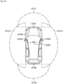
- Fig. 23 is a diagram illustrating an example of an installation position of the imaging portion 12031.
- a vehicle 12100 includes imaging portions 12101, 12102, 12103, 12104, and 12105 as the imaging portion 12031.
- the imaging portions 12101, 12102, 12103, 12104, and 12105 are provided at positions such as a front nose, side-view mirrors, a rear bumper, a back door, and an upper portion of a windshield in a vehicle interior of the vehicle 12100, for example.
- the imaging portion 12101 provided on the front nose and the imaging portion 12105 provided in the upper portion of the windshield in the vehicle interior mainly acquire images of the front of the vehicle 12100.
- the imaging portions 12102 and 12103 provided on the side-view mirrors mainly acquire images of a lateral side of the vehicle 12100.
- the imaging portion 12104 provided on the rear bumper or the back door mainly acquires images of the rear of the vehicle 12100.
- Front view images acquired by the imaging portions 12101 and 12105 are mainly used for detection of preceding vehicles, pedestrians, obstacles, traffic lights, traffic signs, lanes, and the like.
- Fig. 23 illustrates an example of imaging ranges of the imaging portions 12101 to 12104.
- An imaging range 12111 indicates an imaging range of the imaging portion 12101 provided at the front nose
- imaging ranges 12112 and 12113 respectively indicate the imaging ranges of the imaging portions 12102 and 12103 provided at the side-view mirrors
- an imaging range 12114 indicates the imaging range of the imaging portion 12104 provided at the rear bumper or the back door.
- At least one of the imaging portions 12101 to 12104 may have a function for obtaining distance information.
- at least one of the imaging portions 12101 to 12104 may be a stereo camera constituted by a plurality of imaging elements or may be an imaging element that has pixels for phase difference detection.
- the microcomputer 12051 can extract, particularly, the closest three-dimensional object on a path along which the vehicle 12100 is traveling, which is a three-dimensional object traveling at a predetermined speed (for example, 0 km/h or higher) in the substantially same direction as the vehicle 12100, as a vehicle ahead by acquiring a distance to each three-dimensional object in the imaging ranges 12111 to 12114 and a temporal change of this distance (a relative speed with respect to the vehicle 12100) on the basis of the distance information obtained from the imaging portions 12101 to 12104.
- a predetermined speed for example, 0 km/h or higher
- the microcomputer 12051 can set an inter-vehicle distance to be secured from a vehicle ahead in advance with respect to the vehicle ahead and can perform automated brake control (also including following stop control) or automated acceleration control (also including following start control). In this way, cooperative control can be performed for the purpose of automated traveling or the like in which a vehicle automatedly travels without the operations of the driver.
- the microcomputer 12051 can classify and extract three-dimensional data regarding three-dimensional objects into two-wheeled vehicles, normal vehicles, large vehicles, pedestrians, and other three-dimensional objects such as electric poles based on distance information obtained from the imaging portions 12101 to 12104 and can use the three-dimensional data to perform automated avoidance of obstacles.
- the microcomputer 12051 differentiates surrounding obstacles of the vehicle 12100 into obstacles which can be viewed by the driver of the vehicle 12100 and obstacles which are difficult to view.
- the microcomputer 12051 determines a collision risk indicating the degree of risk of collision with each obstacle, and when the collision risk is equal to or higher than a set value and there is a possibility of collision, an alarm is output to the driver through the audio speaker 12061 or the display portion 12062, forced deceleration or avoidance steering is performed through the drive system control unit 12010, and thus it is possible to perform driving support for collision avoidance.
- At least one of the imaging portions 12101 to 12104 may be an infrared camera that detects infrared rays.
- the microcomputer 12051 can recognize a pedestrian by determining whether there is a pedestrian in the captured image of the imaging portions 12101 to 12104.
- pedestrian recognition is performed by, for example, a procedure in which feature points in the captured images of the imaging portions 12101 to 12104 as infrared cameras are extracted and a procedure in which pattern matching processing is performed on a series of feature points indicating an outline of an object to determine whether or not the object is a pedestrian.
- the audio/image output portion 12052 controls the display portion 12062 so that a square contour line for emphasis is superimposed and displayed with the recognized pedestrian.
- the audio/image output portion 12052 may control the display portion 12062 so that an icon indicating a pedestrian or the like is displayed at a desired position.
- the technique according to the present disclosure may be applied to the imaging portion 12031 and the like among the above-described configurations.
- one of the semiconductor devices 200 to 200G described in Embodiments 1 to 8, or the imaging system described in Embodiment 9 are applicable to the imaging portion 12031.
- the technique according to the present disclosure it is possible to improve, for example, the cooling efficiency of the sensor element 40, and obtain a high-quality photographed image, so that the moving body control system can perform accurate control using the photographed image.
- the technology according to the present disclosure for example, it is possible to improve the cooling efficiency for the sensor elements 40, reduce noise or the like caused by the temperature, and obtain a clearer photographed image, so that it is possible to reduce a driver's fatigue.
Landscapes
- Cooling Or The Like Of Semiconductors Or Solid State Devices (AREA)
Applications Claiming Priority (2)
| Application Number | Priority Date | Filing Date | Title |
|---|---|---|---|
| JP2022040650 | 2022-03-15 | ||
| PCT/JP2023/008131 WO2023176522A1 (ja) | 2022-03-15 | 2023-03-03 | 半導体装置 |
Publications (1)
| Publication Number | Publication Date |
|---|---|
| EP4495992A1 true EP4495992A1 (de) | 2025-01-22 |
Family
ID=88022992
Family Applications (1)
| Application Number | Title | Priority Date | Filing Date |
|---|---|---|---|
| EP23770479.6A Withdrawn EP4495992A1 (de) | 2022-03-15 | 2023-03-03 | Halbleiteranordnung |
Country Status (4)
| Country | Link |
|---|---|
| US (1) | US20250194292A1 (de) |
| EP (1) | EP4495992A1 (de) |
| JP (1) | JPWO2023176522A1 (de) |
| WO (1) | WO2023176522A1 (de) |
Families Citing this family (1)
| Publication number | Priority date | Publication date | Assignee | Title |
|---|---|---|---|---|
| CN118510362B (zh) * | 2024-07-18 | 2024-10-29 | 四川科尔威光电科技有限公司 | 一种高集成小型化半导体制冷器及其制备方法 |
Family Cites Families (9)
| Publication number | Priority date | Publication date | Assignee | Title |
|---|---|---|---|---|
| JPH06334197A (ja) * | 1993-05-26 | 1994-12-02 | Matsushita Electric Ind Co Ltd | 半導体装置およびその製造方法 |
| JP4146032B2 (ja) * | 1999-05-31 | 2008-09-03 | 東芝エレベータ株式会社 | 半導体スイッチ装置およびこの半導体スイッチ装置を用いた電力変換装置 |
| JP3608998B2 (ja) * | 2000-03-03 | 2005-01-12 | Necエレクトロニクス株式会社 | 回路装置、パッケージ部材、回路試験方法および装置 |
| JP2008306227A (ja) * | 2008-09-25 | 2008-12-18 | Panasonic Electric Works Co Ltd | 凹凸多層回路板モジュール及びその製造方法 |
| JP5367413B2 (ja) * | 2009-03-02 | 2013-12-11 | ラピスセミコンダクタ株式会社 | 半導体装置 |
| JP6083554B2 (ja) * | 2012-08-07 | 2017-02-22 | 国立大学法人静岡大学 | 撮像モジュール |
| JP2016162781A (ja) * | 2015-02-26 | 2016-09-05 | 京セラ株式会社 | 撮像素子、撮像装置、および撮像素子の製造方法 |
| JP6633151B2 (ja) * | 2018-08-10 | 2020-01-22 | 太陽誘電株式会社 | 回路モジュール |
| JP7566790B2 (ja) * | 2020-01-08 | 2024-10-15 | ソニーセミコンダクタソリューションズ株式会社 | 固体撮像装置、撮像装置及び撮像システム |
-
2023
- 2023-03-03 US US18/843,745 patent/US20250194292A1/en active Pending
- 2023-03-03 EP EP23770479.6A patent/EP4495992A1/de not_active Withdrawn
- 2023-03-03 JP JP2024507745A patent/JPWO2023176522A1/ja active Pending
- 2023-03-03 WO PCT/JP2023/008131 patent/WO2023176522A1/ja not_active Ceased
Also Published As
| Publication number | Publication date |
|---|---|
| WO2023176522A1 (ja) | 2023-09-21 |
| US20250194292A1 (en) | 2025-06-12 |
| JPWO2023176522A1 (de) | 2023-09-21 |
Similar Documents
| Publication | Publication Date | Title |
|---|---|---|
| JP7123813B2 (ja) | 半導体装置、固体撮像素子、並びに電子機器 | |
| US20250194292A1 (en) | Semiconductor device | |
| EP4542647A1 (de) | Verpackung, halbleiterbauelement und verfahren zur herstellung der verpackung | |
| US20240222410A1 (en) | Solid-state imaging apparatus, manufacturing method thereof, and electronic equipment | |
| WO2023248974A1 (ja) | 光検出素子および光検出素子の製造方法 | |
| EP4361670A1 (de) | Lichtempfangselement | |
| US20230361146A1 (en) | Semiconductor apparatus and semiconductor apparatus manufacturing method | |
| US20240413187A1 (en) | Semiconductor apparatus | |
| JP2019161046A (ja) | 半導体装置、撮像装置、および電子機器 | |
| CN116134686A (zh) | 发光装置及其制造方法 | |
| EP4539098A1 (de) | Halbleiterbauelement und bildgebungsvorrichtung | |
| US20260026125A1 (en) | Semiconductor device and electronic apparatus | |
| US20250132237A1 (en) | Semiconductor device and method for manufacturing semiconductor device | |
| US12080636B2 (en) | Semiconductor package and manufacturing method of semiconductor package | |
| WO2024100994A1 (ja) | ペルチェ素子および半導体パッケージ | |
| EP4611042A1 (de) | Verpackung und verfahren zur herstellung der verpackung | |
| EP4693401A1 (de) | Substratvorrichtung, elektronische vorrichtung, elektronische vorrichtung, verfahren zur herstellung einer elektronischen vorrichtung und verfahren zur herstellung einer elektronischen vorrichtung | |
| US12132063B2 (en) | Semiconductor package and method for manufacturing semiconductor package | |
| WO2026083699A1 (ja) | 半導体パッケージ、半導体装置、および、半導体パッケージの製造方法 | |
| WO2024024278A1 (ja) | パッケージおよびパッケージの製造方法 | |
| WO2025115391A1 (ja) | パッケージおよびパッケージの製造方法 | |
| WO2026004347A1 (ja) | 光学パッケージ、モジュール、および、光学パッケージの製造方法 | |
| WO2026034000A1 (ja) | 半導体パッケージ、撮像装置、電子機器、および、半導体パッケージの製造方法 | |
| WO2024224807A1 (ja) | 半導体パッケージ、および、半導体パッケージの製造方法 | |
| WO2026078991A1 (ja) | 半導体装置および半導体装置の製造方法 |
Legal Events
| Date | Code | Title | Description |
|---|---|---|---|
| STAA | Information on the status of an ep patent application or granted ep patent |
Free format text: STATUS: THE INTERNATIONAL PUBLICATION HAS BEEN MADE |
|
| PUAI | Public reference made under article 153(3) epc to a published international application that has entered the european phase |
Free format text: ORIGINAL CODE: 0009012 |
|
| STAA | Information on the status of an ep patent application or granted ep patent |
Free format text: STATUS: REQUEST FOR EXAMINATION WAS MADE |
|
| 17P | Request for examination filed |
Effective date: 20240920 |
|
| AK | Designated contracting states |
Kind code of ref document: A1 Designated state(s): AL AT BE BG CH CY CZ DE DK EE ES FI FR GB GR HR HU IE IS IT LI LT LU LV MC ME MK MT NL NO PL PT RO RS SE SI SK SM TR |
|
| STAA | Information on the status of an ep patent application or granted ep patent |
Free format text: STATUS: THE APPLICATION HAS BEEN WITHDRAWN |
|
| 18W | Application withdrawn |
Effective date: 20250417 |