EP4481472A2 - Antireflexbeschichtungen für metaoberflächen - Google Patents
Antireflexbeschichtungen für metaoberflächen Download PDFInfo
- Publication number
- EP4481472A2 EP4481472A2 EP24211615.0A EP24211615A EP4481472A2 EP 4481472 A2 EP4481472 A2 EP 4481472A2 EP 24211615 A EP24211615 A EP 24211615A EP 4481472 A2 EP4481472 A2 EP 4481472A2
- Authority
- EP
- European Patent Office
- Prior art keywords
- nanostructures
- light
- metasurface
- antireflection coating
- waveguide
- Prior art date
- Legal status (The legal status is an assumption and is not a legal conclusion. Google has not performed a legal analysis and makes no representation as to the accuracy of the status listed.)
- Granted
Links
Images





Classifications
-
- G—PHYSICS
- G02—OPTICS
- G02B—OPTICAL ELEMENTS, SYSTEMS OR APPARATUS
- G02B1/00—Optical elements characterised by the material of which they are made; Optical coatings for optical elements
- G02B1/002—Optical elements characterised by the material of which they are made; Optical coatings for optical elements made of materials engineered to provide properties not available in nature, e.g. metamaterials
-
- G—PHYSICS
- G02—OPTICS
- G02B—OPTICAL ELEMENTS, SYSTEMS OR APPARATUS
- G02B1/00—Optical elements characterised by the material of which they are made; Optical coatings for optical elements
- G02B1/10—Optical coatings produced by application to, or surface treatment of, optical elements
- G02B1/11—Anti-reflection coatings
- G02B1/111—Anti-reflection coatings using layers comprising organic materials
-
- G—PHYSICS
- G02—OPTICS
- G02B—OPTICAL ELEMENTS, SYSTEMS OR APPARATUS
- G02B27/00—Optical systems or apparatus not provided for by any of the groups G02B1/00 - G02B26/00, G02B30/00
- G02B27/0093—Optical systems or apparatus not provided for by any of the groups G02B1/00 - G02B26/00, G02B30/00 with means for monitoring data relating to the user, e.g. head-tracking, eye-tracking
-
- G—PHYSICS
- G02—OPTICS
- G02B—OPTICAL ELEMENTS, SYSTEMS OR APPARATUS
- G02B27/00—Optical systems or apparatus not provided for by any of the groups G02B1/00 - G02B26/00, G02B30/00
- G02B27/01—Head-up displays
- G02B27/017—Head mounted
- G02B27/0172—Head mounted characterised by optical features
-
- G—PHYSICS
- G02—OPTICS
- G02B—OPTICAL ELEMENTS, SYSTEMS OR APPARATUS
- G02B27/00—Optical systems or apparatus not provided for by any of the groups G02B1/00 - G02B26/00, G02B30/00
- G02B27/42—Diffraction optics, i.e. systems including a diffractive element being designed for providing a diffractive effect
- G02B27/4205—Diffraction optics, i.e. systems including a diffractive element being designed for providing a diffractive effect having a diffractive optical element [DOE] contributing to image formation, e.g. whereby modulation transfer function MTF or optical aberrations are relevant
-
- G—PHYSICS
- G02—OPTICS
- G02B—OPTICAL ELEMENTS, SYSTEMS OR APPARATUS
- G02B27/00—Optical systems or apparatus not provided for by any of the groups G02B1/00 - G02B26/00, G02B30/00
- G02B27/42—Diffraction optics, i.e. systems including a diffractive element being designed for providing a diffractive effect
- G02B27/4272—Diffraction optics, i.e. systems including a diffractive element being designed for providing a diffractive effect having plural diffractive elements positioned sequentially along the optical path
-
- G—PHYSICS
- G02—OPTICS
- G02B—OPTICAL ELEMENTS, SYSTEMS OR APPARATUS
- G02B5/00—Optical elements other than lenses
- G02B5/18—Diffraction gratings
- G02B5/1814—Diffraction gratings structurally combined with one or more further optical elements, e.g. lenses, mirrors, prisms or other diffraction gratings
-
- G—PHYSICS
- G02—OPTICS
- G02B—OPTICAL ELEMENTS, SYSTEMS OR APPARATUS
- G02B5/00—Optical elements other than lenses
- G02B5/18—Diffraction gratings
- G02B5/1847—Manufacturing methods
-
- G—PHYSICS
- G02—OPTICS
- G02B—OPTICAL ELEMENTS, SYSTEMS OR APPARATUS
- G02B27/00—Optical systems or apparatus not provided for by any of the groups G02B1/00 - G02B26/00, G02B30/00
- G02B27/01—Head-up displays
- G02B27/0101—Head-up displays characterised by optical features
- G02B2027/014—Head-up displays characterised by optical features comprising information/image processing systems
-
- G—PHYSICS
- G02—OPTICS
- G02B—OPTICAL ELEMENTS, SYSTEMS OR APPARATUS
- G02B27/00—Optical systems or apparatus not provided for by any of the groups G02B1/00 - G02B26/00, G02B30/00
- G02B27/01—Head-up displays
- G02B27/017—Head mounted
- G02B27/0172—Head mounted characterised by optical features
- G02B2027/0174—Head mounted characterised by optical features holographic
-
- G—PHYSICS
- G02—OPTICS
- G02B—OPTICAL ELEMENTS, SYSTEMS OR APPARATUS
- G02B27/00—Optical systems or apparatus not provided for by any of the groups G02B1/00 - G02B26/00, G02B30/00
- G02B27/01—Head-up displays
- G02B27/017—Head mounted
- G02B2027/0178—Eyeglass type
-
- G—PHYSICS
- G02—OPTICS
- G02B—OPTICAL ELEMENTS, SYSTEMS OR APPARATUS
- G02B27/00—Optical systems or apparatus not provided for by any of the groups G02B1/00 - G02B26/00, G02B30/00
- G02B27/01—Head-up displays
- G02B27/0179—Display position adjusting means not related to the information to be displayed
- G02B2027/0185—Displaying image at variable distance
-
- G—PHYSICS
- G02—OPTICS
- G02B—OPTICAL ELEMENTS, SYSTEMS OR APPARATUS
- G02B2207/00—Coding scheme for general features or characteristics of optical elements and systems of subclass G02B, but not including elements and systems which would be classified in G02B6/00 and subgroups
- G02B2207/101—Nanooptics
Definitions
- 62/451,608 entitled “DIFFRACTION GRATINGS FORMED BY METASURFACES HAVING DIFFERENTLY ORIENTED NANOBEAMS,” filed on January 27, 2017 (attorney docket no. MLEAP.092PR); and U.S. Provisional Application No. 62/451,615, entitled “DIFFRACTION GRATINGS BASED ON METASURFACES HAVING ASYMMETRIC OPTICAL ELEMENTS,” filed on January 27, 2017 (attorney docket no. MLEAP.103PR).
- the present disclosure relates to optical systems such as display systems, including augmented reality systems.
- a virtual reality, or "VR” scenario typically involves the presentation of digital or virtual image information without transparency to other actual real-world visual input;
- an augmented reality, or "AR” scenario typically involves presentation of digital or virtual image information as an augmentation to visualization of the actual world around the user.
- a mixed reality, or "MR”, scenario is a type of AR scenario and typically involves virtual objects that are integrated into, and responsive to, the natural world.
- an MR scenario may include AR image content that appears to be blocked by or is otherwise perceived to interact with objects in the real world.
- an augmented reality scene 10 is depicted.
- the user of an AR technology sees a real-world park-like setting 20 featuring people, trees, buildings in the background, and a concrete platform 30.
- the user also perceives that he/she "sees" "virtual content” such as a robot statue 40 standing upon the real-world platform 30, and a flying cartoon-like avatar character 50 which seems to be a personification of a bumble bee.
- These elements 50, 40 are "virtual” in that they do not exist in the real world.
- the human visual perception system is complex, it is challenging to produce AR technology that facilitates a comfortable, natural-feeling, rich presentation of virtual image elements amongst other virtual or real-world imagery elements.
- an optical system may comprise an optically transmissive substrate, a metasurface overlying the substrate, the metasurface comprising a plurality of nanostructures, and an antireflection coating comprising an optically transparent material conformally disposed over the nanostructures of the metasurface, wherein the optically transparent material has a refractive index less than a refractive index of the nanostructures.
- the antireflection coating is an interference coating.
- the metasurface comprises a diffraction grating.
- the metasurface comprises an asymmetric diffraction grating.
- the metasurface comprises a Pancharatnam-Berry phase optical element (PBOE).
- PBOE Pancharatnam-Berry phase optical element
- the metasurface comprises multi-tier nanostructures.
- the optically transparent material comprises a polymer.
- the optically transparent material comprises photoresist.
- the optically transparent material has a refractive index from about 1.2 to about 2.
- a distance from a topmost surface of the nanostructures to a topmost surface of the antireflection coating is from about 10 nm to about 1 micron. In some embodiments, a distance from a topmost surface of the nanostructures to a topmost surface of the antireflection coating is from about 30 nm to about 250 nm. In some embodiments, the antireflection coating forms a planarization layer extending between and over the nanostructures.
- optical systems comprising an antireflection coating for an optical element comprising a metasurface, the antireflection coating comprising a layer of an optically transparent material having a refractive index greater than 1 and less than a refractive index of a material comprising the metasurface, wherein the layer of polymer material layer is conformally disposed over the metasurface.
- the optically transparent material comprises a polymer. In some embodiments, the optically transparent material comprises photoresist. In some embodiments, the optically transparent material has a refractive index from about 1.2 to about 2. In some embodiments, a distance from a topmost surface of the metasurface to a topmost surface of the antireflection coating is from about 10 nm to about 1 micron. In some embodiments, the antireflection coating reduces an amount of incident light reflected by the metasurface by more than about 50% as compared to an amount of incident light reflected by a substantially similar metasurface that does not include the antireflection coating. In some embodiments, the incident light has an incident angle from about -50° to 50°.
- a method may comprise providing an optically transmissive substrate comprising a metasurface, the metasurface comprising a plurality of nanostructures, depositing a layer of an optically transparent material over the plurality of nanostructures, wherein the layer of optically transparent material forms the antireflection coating.
- the optically transparent material comprises a polymer. In some embodiments, the optically transparent material comprises photoresist. In some embodiments, a distance from a topmost surface of the nanostructures to a topmost surface of the formed antireflection coating is from about 10 nm to about 1 micron. In some embodiments, conformally depositing the optically transparent material comprises spin coating the optically transparent material over the nanostructures. In some embodiments, conformally depositing the optically transparent material comprises performing a chemical vapor deposition (CVD) process.
- CVD chemical vapor deposition
- Metasurfaces also referred to as metamaterial surfaces, provide opportunities to realize virtually flat, aberration-free optics on much smaller scales, in comparison with geometrical optics.
- metasurfaces include dense arrangements of surface structures, or nanostructures, that function as resonant optical antennas. The resonant nature of the light-surface structure interaction provides the ability to manipulate optical wave-fronts.
- the metasurfaces may allow the replacement of bulky or difficult to manufacture optical components with thin, planar elements formed by simple patterning processes.
- optical elements formed of metasurfaces may function in the reflective and/or transmissive mode.
- the metasurface In the reflective mode, the metasurface may reflect light at desired angles.
- the metasurface In the transmissive mode, the metasurface may transmit light through the body of the metasurface while also deflecting that light at desired angles.
- metasurfaces working in the transmissive mode may also reflect incident light, e.g., due to Fresnel reflections at interfaces with other materials.
- the angles at which the metasurfaces are configured to reflect light may be different from the angles at which light is reflected off of interfaces.
- metasurfaces may cause optical artifacts.
- image content e.g., light modified by a spatial light modulator
- the reflections may cause ghost images due to the reflection of some of the light back and forth along an optical path before reaching the user.
- metasurfaces may form incoupling optical elements for incoupling light into a waveguide, which in turn is configured to output image content to a user.
- the reflected light may propagate back to a light projector or light source, which may then reflect the light back to the metasurface for incoupling into the waveguide, and ultimately output to a user. Due to this back-and-forth reflection, light from prior video image frames may be provided to the waveguide along with light encoding current image frames. The light encoding prior image frames may be visible to the user as a ghost image that decreases the image quality of the display device.
- an antireflection coating may reduce or eliminate the reflection of light from metasurfaces.
- the antireflection coating may be formed of an optically transmissive layer of material, such as a polymer layer, e.g., a layer of photoresist.
- no air or other material may be present between the metasurface and the antireflection coating; the antireflection coating may directly contact the metasurface.
- the material forming the antireflection coating may have a refractive index lower than the refractive index of the nanostructures of the metasurface, but higher than the refractive index of the material or medium (e.g., air) forming an interface with the antireflective coating opposite the metasurface.
- the antireflection coating may be an interference coating and the thickness of the layer of material is selected to provide destructive interference between light reflecting off the top and bottom surfaces of the layer. Preferably, the thickness of the layer is selected to provide this interference for light of visible wavelengths.
- the metasurfaces may be part of a color display utilizing a plurality of component colors. As a result, a particular metasurface may only be exposed to light of an associated limited range of wavelengths corresponding to a particular component color, and the antireflection coating may have a thickness selected to provide interference for light having this associated limited range of wavelengths.
- the antireflection coating may be a planar layer extending over and between the nanostructures forming the metasurfaces, and forming a planar surface of the nanostructures. Such a planar layer may advantageously provide antireflection properties over a wide range of angles of incident light.
- the antireflection coating may be a conformal layer disposed on the surfaces of the nanostructures forming the metasurfaces. The conformal layer may be continuous and extend over and in between multiple nanostructures, or may be isolated on individual ones of the nanostructures.
- an antireflection coating may reduce the amount of light reflected by a metasurface, relative to identical structure without the antireflection coating, by about 50%, 75%, 85%, 90%, 95%, 99%, or more.
- the antireflection coating may be particularly advantageously applied to metasurfaces operating in the transmissive mode, for which reflections are not part of the design of the metasurface.
- the metasurfaces may advantageously be applied to form optical elements in display devices, such as display devices for AR or VR display systems.
- display systems may display virtual content to a user, or viewer, and AR systems may also allow the user to see the world around them by transmitting light from the surrounding environment to the user's eyes.
- this virtual content is displayed on a wearable head-mounted display, e.g., as part of eyewear, that projects image information to the user's eyes.
- a "head-mounted" display is a display that may be mounted on the head of a viewer.
- FIG. 2 illustrates an example of wearable display system 80.
- the display system 80 includes a head-mounted display 62, and various mechanical and electronic modules and systems to support the functioning of that display 62.
- the display 62 may be coupled to a frame 64, which is wearable by a display system user or viewer 60 and which is configured to position the display 62 in front of the eyes of the user 60.
- the display 62 may be considered eyewear in some embodiments.
- a speaker 66 is coupled to the frame 64 and positioned adj acent the ear canal of the user 60 (in some embodiments, another speaker, not shown, is positioned adjacent the other ear canal of the user to provide for stereo/shapeable sound control).
- the display system may also include one or more microphones 67 or other devices to detect sound.
- the microphone is configured to allow the user to provide inputs or commands to the system 80 (e.g., the selection of voice menu commands, natural language questions, etc.), and/or may allow audio communication with other persons (e.g., with other users of similar display systems.
- the microphone may further be configured as a peripheral sensor to continuously collect audio data (e.g., to passively collect from the user and/or environment).
- Such audio data may include user sounds such as heavy breathing, or environmental sounds, such as a loud bang indicative of a nearby event.
- the display system may also include a peripheral sensor 30a, which may be separate from the frame 64 and attached to the body of the user 60 (e.g., on the head, torso, an extremity, etc. of the user 60).
- the peripheral sensor 30a may be configured to acquire data characterizing the physiological state of the user 60 in some embodiments, as described further herein.
- the sensor 30a may be an electrode.
- FIG. 2 illustrates an example of wearable display system 60.
- the display system 60 includes a display 70, and various mechanical and electronic modules and systems to support the functioning of that display 70.
- the display 70 may be coupled to a frame 80, which is wearable by a display system user or viewer 90 and which is configured to position the display 70 in front of the eyes of the user 90.
- the display 70 may be considered eyewear in some embodiments.
- a speaker 100 is coupled to the frame 80 and configured to be positioned adjacent the ear canal of the user 90 (in some embodiments, another speaker, not shown, may optionally be positioned adjacent the other ear canal of the user to provide stereo/shapeable sound control).
- the display system may also include one or more microphones 110 or other devices to detect sound.
- the microphone is configured to allow the user to provide inputs or commands to the system 60 (e.g., the selection of voice menu commands, natural language questions, etc.), and/or may allow audio communication with other persons (e.g., with other users of similar display systems.
- the microphone may further be configured as a peripheral sensor to collect audio data (e.g., sounds from the user and/or environment).
- the display system may also include a peripheral sensor 120a, which may be separate from the frame 80 and attached to the body of the user 90 (e.g., on the head, torso, an extremity, etc. of the user 90).
- the peripheral sensor 120a may be configured to acquire data characterizing a physiological state of the user 90 in some embodiments.
- the sensor 120a may be an electrode.
- the display 70 is operatively coupled by communications link 130, such as by a wired lead or wireless connectivity, to a local data processing module 140 which may be mounted in a variety of configurations, such as fixedly attached to the frame 80, fixedly attached to a helmet or hat worn by the user, embedded in headphones, or otherwise removably attached to the user 90 (e.g., in a backpack-style configuration, in a belt-coupling style configuration).
- the sensor 120a may be operatively coupled by communications link 120b, e.g., a wired lead or wireless connectivity, to the local processor and data module 140.
- the local processing and data module 140 may comprise a hardware processor, as well as digital memory, such as non-volatile memory (e.g., flash memory or hard disk drives), both of which may be utilized to assist in the processing, caching, and storage of data.
- the data include data a) captured from sensors (which may be, e.g., operatively coupled to the frame 80 or otherwise attached to the user 90), such as image capture devices (such as cameras), microphones, inertial measurement units, accelerometers, compasses, GPS units, radio devices, gyros, and/or other sensors disclosed herein; and/or b) acquired and/or processed using remote processing module 150 and/or remote data repository 160 (including data relating to virtual content), possibly for passage to the display 70 after such processing or retrieval.
- sensors which may be, e.g., operatively coupled to the frame 80 or otherwise attached to the user 90
- image capture devices such as cameras
- microphones such as cameras
- inertial measurement units such as cameras
- accelerometers compasses
- the local processing and data module 140 may be operatively coupled by communication links 170, 180, such as via a wired or wireless communication links, to the remote processing module 150 and remote data repository 160 such that these remote modules 150, 160 are operatively coupled to each other and available as resources to the local processing and data module 140.
- the local processing and data module 140 may include one or more of the image capture devices, microphones, inertial measurement units, accelerometers, compasses, GPS units, radio devices, and/or gyros. In some other embodiments, one or more of these sensors may be attached to the frame 80, or may be standalone structures that communicate with the local processing and data module 140 by wired or wireless communication pathways.
- the remote processing module 150 may comprise one or more processors configured to analyze and process data and/or image information.
- the remote data repository 160 may comprise a digital data storage facility, which may be available through the internet or other networking configuration in a "cloud" resource configuration.
- the remote data repository 160 may include one or more remote servers, which provide information, e.g., information for generating augmented reality content, to the local processing and data module 140 and/or the remote processing module 150.
- all data is stored and all computations are performed in the local processing and data module, allowing fully autonomous use from a remote module.
- the curvature increases with decreasing distance between the object and the eye 210. Consequently, at different depth planes, the degree of divergence of light rays is also different, with the degree of divergence increasing with decreasing distance between depth planes and the viewer's eye 210. While only a single eye 210 is illustrated for clarity of illustration in Figures 5A-5C and other figures herein, it will be appreciated that the discussions regarding eye 210 may be applied to both eyes 210 and 220 of a viewer.
- FIG. 6 illustrates an example of a waveguide stack for outputting image information to a user.
- a display system 250 includes a stack of waveguides, or stacked waveguide assembly, 260 that may be utilized to provide three-dimensional perception to the eye/brain using a plurality of waveguides 270, 280, 290, 300, 310.
- the display system 250 is the system 60 of Figure 2 , with Figure 6 schematically showing some parts of that system 60 in greater detail.
- the waveguide assembly 260 may be part of the display 70 of Figure 2 . It will be appreciated that the display system 250 may be considered a light field display in some embodiments.
- a single waveguide may be configured to output light with a set amount of wavefront divergence corresponding to a single or limited number of depth planes and/or the waveguide may be configured to output light of a limited range of wavelengths. Consequently, in some embodiments, a plurality or stack of waveguides may be utilized to provide different amounts of wavefront divergence for different depth planes and/or to output light of different ranges of wavelengths.
- a depth plane may follow the contours of a flat or a curved surface. In some embodiments, advantageously for simplicity, the depth planes may follow the contours of flat surfaces.
- the waveguide assembly 260 may also include a plurality of features 320, 330, 340, 350 between the waveguides.
- the features 320, 330, 340, 350 may be one or more lenses.
- the waveguides 270, 280, 290, 300, 310 and/or the plurality of lenses 320, 330, 340, 350 may be configured to send image information to the eye with various levels of wavefront curvature or light ray divergence. Each waveguide level may be associated with a particular depth plane and may be configured to output image information corresponding to that depth plane.
- Image injection devices 360, 370, 380, 390, 400 may function as a source of light for the waveguides and may be utilized to inject image information into the waveguides 270, 280, 290, 300, 310, each of which may be configured, as described herein, to distribute incoming light across each respective waveguide, for output toward the eye 210.
- the each of the input surfaces 460, 470, 480, 490, 500 may be an edge of a corresponding waveguide, or may be part of a major surface of the corresponding waveguide (that is, one of the waveguide surfaces directly facing the world 510 or the viewer's eye 210). It will be appreciated that the major surfaces of a waveguide correspond to the relatively large area surfaces of the waveguide between which the thickness of the waveguide extends.
- a single beam of light e.g. a collimated beam
- a single one of the image injection devices 360, 370, 380, 390, 400 may be associated with and inject light into a plurality (e.g., three) of the waveguides 270, 280, 290, 300, 310.
- the image injection devices 360, 370, 380, 390, 400 are discrete displays that each produce image information for injection into a corresponding waveguide 270, 280, 290, 300, 310, respectively.
- the image injection devices 360, 370, 380, 390, 400 are the output ends of a single multiplexed display which may, e.g., pipe image information via one or more optical conduits (such as fiber optic cables) to each of the image injection devices 360, 370, 380, 390, 400.
- the image information provided by the image injection devices 360, 370, 380, 390, 400 may include light of different wavelengths, or colors (e.g., different component colors, as discussed herein).
- the light injected into the waveguides 270, 280, 290, 300, 310 is provided by a light projector system 520, which comprises a light module 530, which may include a light emitter, such as a light emitting diode (LED).
- the light from the light module 530 may be directed to and modified by a light modulator 540, e.g., a spatial light modulator, via a beam splitter 550.
- the light modulator 540 may be configured to change the perceived intensity of the light injected into the waveguides 270, 280, 290, 300, 310 to encode the light with image information.
- Examples of spatial light modulators include liquid crystal displays (LCD) including a liquid crystal on silicon (LCOS) displays.
- the image injection devices 360, 370, 380, 390, 400 are illustrated schematically and, in some embodiments, these image injection devices may represent different light paths and locations in a common projection system configured to output light into associated ones of the waveguides 270, 280, 290, 300, 310.
- the waveguides of the waveguide assembly 260 may function as ideal lens while relaying light injected into the waveguides out to the user's eyes.
- the object may be the spatial light modulator 540 and the image may be the image on the depth plane.
- the display system 250 may be a scanning fiber display comprising one or more scanning fibers configured to project light in various patterns (e.g., raster scan, spiral scan, Lissajous patterns, etc.) into one or more waveguides 270, 280, 290, 300, 310 and ultimately to the eye 210 of the viewer.
- the illustrated image injection devices 360, 370, 380, 390, 400 may schematically represent a single scanning fiber or a bundle of scanning fibers configured to inject light into one or a plurality of the waveguides 270, 280, 290, 300, 310.
- the illustrated image injection devices 360, 370, 380, 390, 400 may schematically represent a plurality of scanning fibers or a plurality of bundles of scanning fibers, each of which are configured to inject light into an associated one of the waveguides 270, 280, 290, 300, 310. It will be appreciated that one or more optical fibers may be configured to transmit light from the light module 530 to the one or more waveguides 270, 280, 290, 300, 310.
- one or more intervening optical structures may be provided between the scanning fiber, or fibers, and the one or more waveguides 270, 280, 290, 300, 310 to, e.g., redirect light exiting the scanning fiber into the one or more waveguides 270, 280, 290, 300, 310.
- a controller 560 controls the operation of one or more of the stacked waveguide assembly 260, including operation of the image injection devices 360, 370, 380, 390, 400, the light source 530, and the light modulator 540.
- the controller 560 is part of the local data processing module 140.
- the controller 560 includes programming (e.g., instructions in a non-transitory medium) that regulates the timing and provision of image information to the waveguides 270, 280, 290, 300, 310 according to, e.g., any of the various schemes disclosed herein.
- the controller may be a single integral device, or a distributed system connected by wired or wireless communication channels.
- the controller 560 may be part of the processing modules 140 or 150 ( Figure 2 ) in some embodiments.
- the waveguides 270, 280, 290, 300, 310 may be configured to propagate light within each respective waveguide by total internal reflection (TIR).
- the waveguides 270, 280, 290, 300, 310 may each be planar or have another shape (e.g., curved), with major top and bottom surfaces and edges extending between those major top and bottom surfaces.
- the waveguides 270, 280, 290, 300, 310 may each include out-coupling optical elements 570, 580, 590, 600, 610 that are configured to extract light out of a waveguide by redirecting the light, propagating within each respective waveguide, out of the waveguide to output image information to the eye 210.
- Extracted light may also be referred to as out-coupled light and the out-coupling optical elements light may also be referred to light extracting optical elements.
- An extracted beam of light may be outputted by the waveguide at locations at which the light propagating in the waveguide strikes a light extracting optical element.
- the out-coupling optical elements 570, 580, 590, 600, 610 may, for example, be gratings, including diffractive optical features, as discussed further herein.
- the out-coupling optical elements 570, 580, 590, 600, 610 may be disposed at the top and/or bottom major surfaces, and/or may be disposed directly in the volume of the waveguides 270, 280, 290, 300, 310, as discussed further herein.
- the out-coupling optical elements 570, 580, 590, 600, 610 may be formed in a layer of material that is attached to a transparent substrate to form the waveguides 270, 280, 290, 300, 310.
- the waveguides 270, 280, 290, 300, 310 may be a monolithic piece of material and the out-coupling optical elements 570, 580, 590, 600, 610 may be formed on a surface and/or in the interior of that piece of material.
- each waveguide 270, 280, 290, 300, 310 is configured to output light to form an image corresponding to a particular depth plane.
- the waveguide 270 nearest the eye may be configured to deliver collimated light (which was injected into such waveguide 270), to the eye 210.
- the collimated light may be representative of the optical infinity focal plane.
- the next waveguide up 280 may be configured to send out collimated light which passes through the first lens 350 (e.g., a negative lens) before it can reach the eye 210; such first lens 350 may be configured to create a slight convex wavefront curvature so that the eye/brain interprets light coming from that next waveguide up 280 as coming from a first focal plane closer inward toward the eye 210 from optical infinity.
- first lens 350 e.g., a negative lens
- the third up waveguide 290 passes its output light through both the first 350 and second 340 lenses before reaching the eye 210; the combined optical power of the first 350 and second 340 lenses may be configured to create another incremental amount of wavefront curvature so that the eye/brain interprets light coming from the third waveguide 290 as coming from a second focal plane that is even closer inward toward the person from optical infinity than was light from the next waveguide up 280.
- the other waveguide layers 300, 310 and lenses 330, 320 are similarly configured, with the highest waveguide 310 in the stack sending its output through all of the lenses between it and the eye for an aggregate focal power representative of the closest focal plane to the person.
- a compensating lens layer 620 may be disposed at the top of the stack to compensate for the aggregate power of the lens stack 320, 330, 340, 350 below.
- Such a configuration provides as many perceived focal planes as there are available waveguide/lens pairings.
- Both the out-coupling optical elements of the waveguides and the focusing aspects of the lenses may be static (i.e., not dynamic or electro-active). In some alternative embodiments, either or both may be dynamic using electro-active features.
- two or more of the waveguides 270, 280, 290, 300, 310 may have the same associated depth plane.
- multiple waveguides 270, 280, 290, 300, 310 may be configured to output images set to the same depth plane, or multiple subsets of the waveguides 270, 280, 290, 300, 310 may be configured to output images set to the same plurality of depth planes, with one set for each depth plane. This can provide advantages for forming a tiled image to provide an expanded field of view at those depth planes.
- a camera assembly 630 may be provided to capture images of the eye 210 and/or tissue around the eye 210 to, e.g., detect user inputs and/or to monitor the physiological state of the user.
- a camera may be any image capture device.
- the camera assembly 630 may include an image capture device and a light source to project light (e.g., infrared light) to the eye, which may then be reflected by the eye and detected by the image capture device.
- G is the color green
- R is the color red
- B is the color blue.
- other colors associated with other wavelengths of light including magenta and cyan, may be used in addition to or may replace one or more of red, green, or blue.
- the light source 530 ( Figure 6 ) may be configured to emit light of one or more wavelengths outside the visual perception range of the viewer, for example, infrared and/or ultraviolet wavelengths.
- the in-coupling, out-coupling, and other light redirecting structures of the waveguides of the display 250 may be configured to direct and emit this light out of the display towards the user's eye 210, e.g., for imaging and/or user stimulation applications.
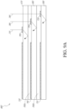
- FIG. 9A illustrates a cross-sectional side view of an example of a plurality or set 660 of stacked waveguides that each includes an in-coupling optical element.
- the waveguides may each be configured to output light of one or more different wavelengths, or one or more different ranges of wavelengths.
- the illustrated set 660 of stacked waveguides includes waveguides 670, 680, and 690.
- Each waveguide includes an associated in-coupling optical element (which may also be referred to as a light input area on the waveguide), with, e.g., in-coupling optical element 700 disposed on a major surface (e.g., an upper major surface) of waveguide 670, in-coupling optical element 710 disposed on a major surface (e.g., an upper major surface) of waveguide 680, and in-coupling optical element 720 disposed on a major surface (e.g., an upper major surface) of waveguide 690.
- in-coupling optical element 700 disposed on a major surface (e.g., an upper major surface) of waveguide 670
- in-coupling optical element 710 disposed on a major surface (e.g., an upper major surface) of waveguide 680
- in-coupling optical element 720 disposed on a major surface (e.g., an upper major surface
- one or more of the in-coupling optical elements 700, 710, 720 may be disposed on the bottom major surface of the respective waveguide 670, 680, 690 (particularly where the one or more in-coupling optical elements are reflective, deflecting optical elements). As illustrated, the in-coupling optical elements 700, 710, 720 may be disposed on the upper major surface of their respective waveguide 670, 680, 690 (or the top of the next lower waveguide), particularly where those in-coupling optical elements are transmissive, deflecting optical elements. In some embodiments, the in-coupling optical elements 700, 710, 720 may be disposed in the body of the respective waveguide 670, 680, 690.
- the in-coupling optical elements 700, 710, 720 are wavelength selective, such that they selectively redirect one or more wavelengths of light, while transmitting other wavelengths of light. While illustrated on one side or corner of their respective waveguide 670, 680, 690, it will be appreciated that the in-coupling optical elements 700, 710, 720 may be disposed in other areas of their respective waveguide 670, 680, 690 in some embodiments.
- Each waveguide also includes associated light distributing elements, with, e.g., light distributing elements 730 disposed on a major surface (e.g., a top major surface) of waveguide 670, light distributing elements 740 disposed on a major surface (e.g., a top major surface) of waveguide 680, and light distributing elements 750 disposed on a major surface (e.g., a top major surface) of waveguide 690.
- the light distributing elements 730, 740, 750 may be disposed on a bottom major surface of associated waveguides 670, 680, 690, respectively.
- the light distributing elements 730, 740, 750 may be disposed on both top and bottom major surface of associated waveguides 670, 680, 690, respectively; or the light distributing elements 730, 740, 750, may be disposed on different ones of the top and bottom major surfaces in different associated waveguides 670, 680, 690, respectively.
- the waveguides 670, 680, 690 may be spaced apart and separated by, e.g., gas, liquid, and/or solid layers of material.
- layer 760a may separate waveguides 670 and 680; and layer 760b may separate waveguides 680 and 690.
- the layers 760a and 760b are formed of low refractive index materials (that is, materials having a lower refractive index than the material forming the immediately adjacent one of waveguides 670, 680, 690).
- the refractive index of the material forming the layers 760a, 760b is 0.05 or more, or 0.10 or less than the refractive index of the material forming the waveguides 670, 680, 690.
- the lower refractive index layers 760a, 760b may function as cladding layers that facilitate total internal reflection (TIR) of light through the waveguides 670, 680, 690 (e.g., TIR between the top and bottom major surfaces of each waveguide).
- TIR total internal reflection
- the layers 760a, 760b are formed of air. While not illustrated, it will be appreciated that the top and bottom of the illustrated set 660 of waveguides may include immediately neighboring cladding layers.
- light rays 770, 780, 790 are incident on the set 660 of waveguides. It will be appreciated that the light rays 770, 780, 790 may be injected into the waveguides 670, 680, 690 by one or more image injection devices 360, 370, 380, 390, 400 ( Figure 6 ).
- the light rays 770, 780, 790 have different properties, e.g., different wavelengths or different ranges of wavelengths, which may correspond to different colors.
- the in-coupling optical elements 700, 710, 720 each deflect the incident light such that the light propagates through a respective one of the waveguides 670, 680, 690 by TIR.
- the incoupling optical elements 700, 710, 720 each selectively deflect one or more particular wavelengths of light, while transmitting other wavelengths to an underlying waveguide and associated incoupling optical element.
- in-coupling optical element 700 may be configured to deflect ray 770, which has a first wavelength or range of wavelengths, while transmitting rays 1242 and 1244, which have different second and third wavelengths or ranges of wavelengths, respectively.
- the transmitted ray 780 impinges on and is deflected by the in-coupling optical element 710, which is configured to deflect light of a second wavelength or range of wavelengths.
- the ray 790 is deflected by the in-coupling optical element 720, which is configured to selectively deflect light of third wavelength or range of wavelengths.
- the deflected light rays 770, 780, 790 are deflected so that they propagate through a corresponding waveguide 670, 680, 690; that is, the in-coupling optical elements 700, 710, 720 of each waveguide deflects light into that corresponding waveguide 670, 680, 690 to in-couple light into that corresponding waveguide.
- the light rays 770, 780, 790 are deflected at angles that cause the light to propagate through the respective waveguide 670, 680, 690 by TIR.
- the light rays 770, 780, 790 propagate through the respective waveguide 670, 680, 690 by TIR until impinging on the waveguide's corresponding light distributing elements 730, 740, 750.
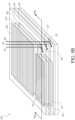
- FIG. 9B a perspective view of an example of the plurality of stacked waveguides of Figure 9A is illustrated.
- the in-coupled light rays 770, 780, 790 are deflected by the in-coupling optical elements 700, 710, 720, respectively, and then propagate by TIR within the waveguides 670, 680, 690, respectively.
- the light rays 770, 780, 790 then impinge on the light distributing elements 730, 740, 750, respectively.
- the light distributing elements 730, 740, 750 deflect the light rays 770, 780, 790 so that they propagate towards the out-coupling optical elements 800, 810, 820, respectively.
- the light distributing elements 730, 740, 750 are orthogonal pupil expanders (OPE's).
- OPE's deflect or distribute light to the out-coupling optical elements 800, 810, 820 and, in some embodiments, may also increase the beam or spot size of this light as it propagates to the out-coupling optical elements.
- the light distributing elements 730, 740, 750 may be omitted and the in-coupling optical elements 700, 710, 720 may be configured to deflect light directly to the out-coupling optical elements 800, 810, 820.
- the light distributing elements 730, 740, 750 may be replaced with out-coupling optical elements 800, 810, 820, respectively.
- the out-coupling optical elements 800, 810, 820 are exit pupils (EP's) or exit pupil expanders (EPE's) that direct light in a viewer's eye 210 ( Figure 7 ).
- the OPE's may be configured to increase the dimensions of the eye box in at least one axis and the EPE's may be to increase the eye box in an axis crossing, e.g., orthogonal to, the axis of the OPEs.
- each OPE may be configured to redirect a portion of the light striking the OPE to an EPE of the same waveguide, while allowing the remaining portion of the light to continue to propagate down the waveguide.
- another portion of the remaining light is redirected to the EPE, and the remaining portion of that portion continues to propagate further down the waveguide, and so on.
- a portion of the impinging light is directed out of the waveguide towards the user, and a remaining portion of that light continues to propagate through the waveguide until it strikes the EP again, at which time another portion of the impinging light is directed out of the waveguide, and so on.
- a single beam of incoupled light may be "replicated" each time a portion of that light is redirected by an OPE or EPE, thereby forming a field of cloned beams of light, as shown in Figure 6 .
- the OPE and/or EPE may be configured to modify a size of the beams of light.
- the set 660 of waveguides includes waveguides 670, 680, 690; in-coupling optical elements 700, 710, 720; light distributing elements (e.g., OPE's) 730, 740, 750; and out-coupling optical elements (e.g., EP's) 800, 810, 820 for each component color.
- the waveguides 670, 680, 690 may be stacked with an air gap/cladding layer between each one.
- the in-coupling optical elements 700, 710, 720 redirect or deflect incident light (with different in-coupling optical elements receiving light of different wavelengths) into its waveguide.
- light ray 770 (e.g., blue light) is deflected by the first in-coupling optical element 700, and then continues to bounce down the waveguide, interacting with the light distributing element (e.g., OPE's) 730 and then the out-coupling optical element (e.g., EPs) 800, in a manner described earlier.
- the light rays 780 and 790 (e.g., green and red light, respectively) will pass through the waveguide 670, with light ray 780 impinging on and being deflected by in-coupling optical element 710.
- the light ray 780 then bounces down the waveguide 680 via TIR, proceeding on to its light distributing element (e.g., OPEs) 740 and then the out-coupling optical element (e.g., EP's) 810.
- light ray 790 (e.g., red light) passes through the waveguide 690 to impinge on the light in-coupling optical elements 720 of the waveguide 690.
- the light in-coupling optical elements 720 deflect the light ray 790 such that the light ray propagates to light distributing element (e.g., OPEs) 750 by TIR, and then to the out-coupling optical element (e.g., EPs) 820 by TIR.
- the out-coupling optical element 820 then finally out-couples the light ray 790 to the viewer, who also receives the out-coupled light from the other waveguides 670, 680.
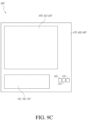
- Figure 9C illustrates a top-down plan view of an example of the plurality of stacked waveguides of Figures 9A and 9B .
- the waveguides 670, 680, 690, along with each waveguide's associated light distributing element 730, 740, 750 and associated out-coupling optical element 800, 810, 820 may be vertically aligned.
- the in-coupling optical elements 700, 710, 720 are not vertically aligned; rather, the in-coupling optical elements are preferably non-overlapping (e.g., laterally spaced apart as seen in the top-down view).
- this nonoverlapping spatial arrangement facilitates the injection of light from different resources into different waveguides on a one-to-one basis, thereby allowing a specific light source to be uniquely coupled to a specific waveguide.
- arrangements including nonoverlapping spatially-separated in-coupling optical elements may be referred to as a shifted pupil system, and the in-coupling optical elements within these arrangements may correspond to sub pupils.
- an example optical structure 1400 comprising a metasurface 1418 formed by a plurality of nanostructures 1420 and an antireflection coating 1430 disposed directly over the nanostructures 1420.
- the metasurface 1418 and antireflection coating 1430 may be disposed on an optically transmissive substrate 1410.
- the antireflection coating 1430 fills the spaces between the nanostructures 1420 such that no air or other material is disposed between the nanostructures 1420 and the antireflection coating 1430, at least over the majority of the expanse of the metasurface 1418.
- the antireflection coating 1430 may be optically transmissive or substantially transmissive to light.
- the antireflection coating 1430 may provide impedance matching between an overlying medium (e.g., air) and one or both of the nanostructures 1420 and the substrate 1410, to reduced occurrence of reflections. It is also believed that the antireflection coating 1430 may cause destructive interference between light reflected from the top surface of the antireflection coating 1430a and bottom surface of the antireflection coating 1430b and/or light backscattered from the surfaces of the nanostructures 1420 and/or the surface of the substrate 1410. This interference is believed to lead to a reduction or elimination in the amount of light perceived to be reflected from the optical structure 1400.
- an overlying medium e.g., air
- the antireflection coating 1430 may comprise an optically transmissive material having a refractive index lower than the refractive index of the nanostructures 1420, but higher than the refractive index of the medium or material directly overlying and forming an interface with the antireflective coating 1430.
- the medium overlying and forming an interface with the antireflective coating 1430 may be air.
- the antireflection coating 1430 may have a refractive index of from about 1.2 to about 2.0, from about 1.2 to about 1.7, from about 1.3 to about 1.6, or from about 1.4 to about 1.5. In some embodiments, the antireflection coating 1430 may have a refractive index of about 1.45.
- the metasurface 1418 comprising a plurality of nanostructures 1420 may be configured to manipulate light, such as for beam steering, wavefront shaping, separating wavelengths and/or polarizations, and combining different wavelengths and/or polarizations.
- the light is visible light having a wavelength in the range of 350 nm to 800 nm.
- the metasurface over which an antireflection coating is disposed may comprise nanostructures having a size and periodicity less than the wavelength of the visible light. It will be appreciated that, in some embodiments, the metasurface 1418 selectively redirects some wavelengths of light, while allowing other wavelengths of light to pass without being redirected.
- Such properties are typically engineered with structures on micron scales (e.g., in photonics crystal fibers or distributed bragg reflectors), while various embodiments herein include geometries on nano-scales (e.g. 10-100x smaller scales), and provide selective redirection of light in the visible part of the electromagnetic spectrum.
- micron scales e.g., in photonics crystal fibers or distributed bragg reflectors
- nano-scales e.g. 10-100x smaller scales
- the metasurface 1418 may work in a transmissive mode in which light is incident on the metasurface from a first side of the metasurface 1418, propagates through the body of the metasurface 1418, and subsequently propagates away from the metasurface 1418 on an opposite side of the metasurface 1418. The light propagates away from the metasurface 1418 in a direction different from the incident direction of the light on the first side.
- an antireflection coating 1430 may reduce or eliminate the amount of light reflected from the metasurface 1418 as compared to a metasurface 1418 that does not comprise an antireflection coating 1430. In some embodiments, the antireflection coating 1430 may not substantially reduce or impact the amount of light that propagates through and away from the metasurface 1418 as compared to a metasurface 1418 that does not comprise an antireflection coating 1430.
- the substrate 1410 supporting the metasurfaces 1418 over which an antireflection coating 1430 is disposed may be a waveguide and may form direct view display devices or near-eye display devices, with the waveguides configured to receive input image information and generate an output image based on the input image information in the form of light encoded with image information. These devices may be wearable and constitute eyewear in some embodiments, and may be the display devices described herein with respect to Figures 1-9C .
- the input image information received by the waveguides may be encoded in multiplexed light streams of different wavelengths (e.g., red, green and blue light) that are incoupled into one or more waveguides. Incoupled light may propagate through the waveguide due to total internal reflection. The incoupled light may be outcoupled (or outputted) from the waveguide by one or more outcoupling optical elements, as described above regarding Figures 9A-9C .
- the metasurfaces 1418 over which an antireflection coating 1430 is conformally disposed may be the incoupling optical elements, outcoupling optical elements, and/or light distributing elements of the waveguide.
- the compactness and planarity of the metasurface 1418 and antireflection coating 1430 allows for a compact waveguide, and for a compact stack of waveguides where multiple waveguides form a stack.
- the metasurface 1418 may be configured to provide for a high degree of precision in incoupling and/or outcoupling light, which may provide high image quality.
- the high selectivity may reduce channel crosstalk in configurations in which full color images are formed by outputting light of different colors or wavelengths at the same time, while the antireflection coating 1430 may reduce ghost images.
- the nanostructures 1420 may have various sizes and be arranged in various orientations relative to one another to form the metasurface 1418 for various applications.
- the nanostructures 1420 may be arranged to form a diffraction grating, such as asymmetric or an asymmetric diffraction grating.
- the metasurface 1418 may be formed of nanostructures 1420 that are a multilevel or tiered.
- the nanostructures 1420 may be relatively wide on a first level and relatively narrower on a second level.
- the metasurfaces 1418 may be formed on a single level, and have a substantially constant width on that level.
- the optical structure 1400 may be any metasurface comprising a plurality of nanostructures as is known in the art or developed in the future.
- nanostructures 1420 Examples of different configurations of the nanostructures 1420 are described below. It will be appreciated that, for clarity of description, the nanostructures discussed below may have different reference numerals than 1420. Nevertheless, it will be understood that the various nanostructures (1520, 1620) described below correspond to the nanostructures 1420 of Figure 10 .
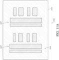
- an example optical element 1500 comprising an asymmetric Pancharatnam-Berry Phase Optical Element (PBOE) and including an antireflection coating 1430 is illustrated.
- the antireflection coating 1430 follows the contours of the nanostructures 1520 such that substantially no air or other material is present between the nanostructures 1520 and the antireflection coating 1430.
- the antireflection coating 1430 may have a substantially flat top surface 1430a.
- the antireflection coating 1430 may function as a planarization layer for the underlying uneven topology of the nanostructures 1520.
- Figure 11C is a plot of transmission and reflection as a function of the angle of incidence of light for an optical structure having the general structure described with reference to Figures 11A - 11B .
- Various orders of diffracted transmitted light are indicated by "T” and reflected light is indicated by "R.”
- the antireflection coating 1430 is an optically transmissive photoresist having a refractive index of about 1.45, which is lower than the refractive index of the nanostructures 1520 and lower than the refractive index of the substrate 1410, which is about 1.77 and formed of polysilicon.
- the thickness 1522 of the antireflection coating 1430 is about 50 nm and air forms an interface with the topmost surface of the antireflection coating 1430.
- a metasurface 1518 comprising an antireflection coating 1430 may be used as an optical element 1500 as described herein, for example an incoupling optical element, without a substantial reduction in the amount of incoupled light, while reducing the amount of reflected light, thereby reducing or eliminating potential ghost images in the display device in which the optical element is incorporated.
- Figure 12C is a plot of the transmission and reflection spectrum for an optical element having the general structure shown in Figures 12A - 12B .
- the percentage of incident light reflected from the optical element 1600 comprising the antireflection coating 1430 remains below about 2% over a wide range of incident angles, from more than -30° to more than 30°.
- the percentage of light reflected from the optical element 1600 comprising the antireflection coating 1430 is about 0 for incident angles from about -15° to about 15°.
- an optical element 1600 comprising an antireflection coating 1430 may be used as an optical element as described herein, for example an incoupling optical element, without a substantial reduction in the amount of incoupled light, while reducing the amount of reflected light, thereby reducing or eliminating potential ghost images, as discussed herein.
- the metal surfaces and nanostructures disclosed herein may be formed by patterning, such as patterning by lithography and etching.
- the metasurfaces and nanostructures may be patterned using nanoimprinting, thereby avoiding costly lithography and etch processes.
- any masking materials may be removed in some embodiments and an antireflection coating 1430 may be applied, deposited, or formed over the metasurface, as described herein.
- the masking materials themselves may be utilized as the antireflective coating.
- Figures 13A-13D and Figures 14A-14D illustrate examples of process flows for forming optical structures having antireflection coatings.
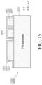
- Figures 13A-13D illustrate cross-sectional views of intermediate structures 1700A-1700D, respectively, at various stages of fabrication of an optical element 1400, 1500 1600 having a metasurface 1418, 1518, 1618 using lithography and etch, according to some embodiments.
- the method includes providing a substrate 1410 having a surface 1410S suitable for forming a metasurface 1418, 1518, 1618 thereon.
- the substrate 1410 includes an optically transmissive material having a refractive index n 2 and various other material attributes described above with reference to Figure 10 .
- the method additionally includes forming on the surface 1410S a high index layer 1411 having an index of refraction n 1 bulk .
- the high index layer 1411 is suitable, when patterned, for forming the one or more nanostructure 1420, 1520, 1620, as described above with reference to Figures 10-12 .
- the high index layer 1411 may be deposited using any suitable technique, such as chemical vapor deposition (CVD), including plasma-based CVD processes, such as plasma-enhanced chemical vapor deposition (PECVD) and thermal-based CVD processes, such as low pressure chemical vapor deposition (LPCVD), according to some embodiments.
- the high index layer 1411 may also be deposited using physical vapor deposition (PVD), evaporation, and atomic layer deposition, among other techniques.
- the method additionally includes forming on the high index layer 1411 a masking layer 1431A.
- the masking layer 1431A may be formed of or include one or more layers of materials that are suitable for providing a template for subsequent etching of the underlying high index layer 1411.
- the masking layer 1431A may be a photoresist, which may be spin-coated, followed by a post-bake.
- the masking layer 1431A may include a plurality of layers, including a hard mask layer formed on the high index layer 1411 and a photoresist layer formed on the hard mask layer. The hard mask layer may be included, for example, when a photoresist layer may not provide sufficient etch selectivity during the subsequent etch pattern transfer to the underlying high index layer 1411.
- the hard mask layer may also serve as an antireflective coating to minimize reflection during the subsequent exposure process.
- the hard mask layer may be a spin-coated polymer or a film deposited by any of the deposition techniques for depositing the high index layer 1411.
- the hard mask layer may provide greater etch selectivity than the overlying photoresist layer.
- the photoresist may be a positive photoresist or a negative photoresist.
- a positive photoresist is a type of photoresist in which the portion of the photoresist that is exposed to light becomes soluble to the photoresist developer
- a negative resist is a type of photoresist in which the portion of the photoresist that is exposed to light becomes insoluble to the photoresist developer.
- the photoresist and/or the hard mask layer may be formed of a material containing silicon or silicon oxide, which may have sufficient etch selectivity against the high index layer 1411, such that the photoresist and/or the hard mask layer remains relatively intact through the etching of the underlying high-index layer 1411.
- the silicon or silicon oxide-containing photoresist and/or hard mask layer may remain on top of one or more nanostructures 1420, 1520, 1620 after patterning, as described above with reference to Figures 10-12 .
- the method includes patterning the photoresist layer of the mask layer 1431 by selectively exposing portions of the photoresist to a pattern of light.
- the exposure to light e.g., coherent UV light, or an electron beam, causes a chemical change, e.g., polymeric crosslinking in the photoresist, which allows exposed portions of the photoresist to be selectively removed by a developer solution for a positive photoresist, or allows unexposed portions of the photoresist to be selectively removed by a developer solution for a negative photoresist.
- the resulting patterned masking photoresist Upon selectively removing, the resulting patterned masking photoresist remains on the high index layer 1411, thereby serving as a template for the subsequent patterning the underlying hard mask layer when included by, e.g., etching.
- the resulting intermediate structure 1700C shows the patterned masking layer 1411, which includes the patterned photoresist and optionally the patterned hard mask layer when included.
- the patterned masking layer 1431 may be used as a template to etch the underlying high index layer 1411 into one or more nanostructures 1420, 1520, 1620.
- the nanostructures 1420, 1520, 1620 may be configured as desired based on the desired properties of the resulting meta-surface.
- the nanostructures 1420, 1520, 1620 may include features extending in a first lateral direction (e.g., the y-direction) and a plurality of second nanostructures 1420, 1520, 1620 extending in a second direction (e.g., the x-direction), as described more in detail above with reference to Figures 10-12 .
- the high index layer 1411 may be etched, e.g., anisotropically dry-etched.
- the etch process employed may have a suitable selectivity against the masking layer 1431 and/or the substrate 1410, such that the portions of the high index layer 1411 are removed without prematurely removing the masking layer 1431 and/or without undesirably damaging the exposes portions of the substrate 1410.
- the masking layer 1431 on the one or more nanostructures 1420, 1520, 1620 are removed therefrom.
- the resist portion of the masking layer 1431 may be removed by, e.g., using a liquid resist stripper or an oxygen-based plasma in a process referred to as ashing.
- the underlying hard mask layer may be subsequently removed using a wet or a dry etch process which selectively removes the hard mask without substantially affecting the one or more nanostructures 1420, 1520, 1620 or the substrate 1410.
- an antireflective coating may be deposited on and at the sides of the nanostructures 1420, 1520, 1620, e.g. by spin-coating or by chemical vapor deposition and subsequent planarization of the vapor deposited layer.
- the mask layer 1431 e.g., the photoresist/hard mask or the hard mask, may be left-in without being removed.
- the mask layer 1431 may comprise the anti-reflection coating 1430 as described herein with reference to Figures 10-12
- Figures 14A-14D illustrate cross-sectional views of intermediate structures 1800A-1800D, respectively, at various stages of fabrication of an optical element 1400, 1500, 1600 having a metasurface 1418, 1518, 1618 according to some embodiments.
- the method of forming intermediate structures 1800A, 1800C and 1800D of Figures 14A, 14C and 14D is similar to the method of forming intermediate structures 1700A, 1700C and 1700D of Figures 13A, 13C and 13D , respectively.
- the method of forming the intermediate structure 1800B of Figure 14B is different from the method forming the intermediate structure 1700B of Figure 13B , whose differences are described below.
- a nanoimprint template 1432, or a nanoimprint mold which has predefined topological patterns in accordance with formation of the one or more nanostructure 1420, 1520, 1620, is brought into contact with an imprint resist of the masking layer 1431A.
- the template 1432 is pressed into an imprint resist formed of thermoplastic polymer under certain temperature, e.g., above the glass transition temperature of the imprint resist, thereby transferring the pattern of the template 1432 into the softened imprint resist.
- the template 1432 is separated from the imprint resist and the patterned resist is left on the high index layer 1411.
- the imprint resist is hardened by crosslinking under UV light.
- an antireflective coating 1430 may be conformally deposited on the nanostructures 1420, 1520, 1620, e.g. by a vapor deposition process such as a chemical vapor deposition process or atomic layer deposition process.
- the deposited antireflective coating 1430 may a conformal layer overlying the nanostructures 1420, 1520, 1620, and following contours of the nanostructures 1420, 1520, 1620, without completely filling the volume separating those nanostructures.
- conditional language used herein such as, among others, “can,” “could,” “might,” “may,” “e.g.,” and the like, unless specifically stated otherwise, or otherwise understood within the context as used, is generally intended to convey that certain embodiments include, while other embodiments do not include, certain features, elements and/or steps. Thus, such conditional language is not generally intended to imply that features, elements and/or steps are in any way required for one or more embodiments or that one or more embodiments necessarily include logic for deciding, with or without author input or prompting, whether these features, elements and/or steps are included or are to be performed in any particular embodiment.
Landscapes
- Physics & Mathematics (AREA)
- General Physics & Mathematics (AREA)
- Optics & Photonics (AREA)
- Engineering & Computer Science (AREA)
- Manufacturing & Machinery (AREA)
- Surface Treatment Of Optical Elements (AREA)
- Devices For Indicating Variable Information By Combining Individual Elements (AREA)
- Diffracting Gratings Or Hologram Optical Elements (AREA)
- Mechanical Optical Scanning Systems (AREA)
Applications Claiming Priority (3)
| Application Number | Priority Date | Filing Date | Title |
|---|---|---|---|
| US201762451587P | 2017-01-27 | 2017-01-27 | |
| EP18744218.1A EP3574350B1 (de) | 2017-01-27 | 2018-01-24 | Antireflexbeschichtungen für metaoberflächen |
| PCT/US2018/015057 WO2018140502A1 (en) | 2017-01-27 | 2018-01-24 | Antireflection coatings for metasurfaces |
Related Parent Applications (1)
| Application Number | Title | Priority Date | Filing Date |
|---|---|---|---|
| EP18744218.1A Division EP3574350B1 (de) | 2017-01-27 | 2018-01-24 | Antireflexbeschichtungen für metaoberflächen |
Publications (3)
| Publication Number | Publication Date |
|---|---|
| EP4481472A2 true EP4481472A2 (de) | 2024-12-25 |
| EP4481472A3 EP4481472A3 (de) | 2025-01-01 |
| EP4481472B1 EP4481472B1 (de) | 2026-04-22 |
Family
ID=62979647
Family Applications (2)
| Application Number | Title | Priority Date | Filing Date |
|---|---|---|---|
| EP24211615.0A Active EP4481472B1 (de) | 2017-01-27 | 2018-01-24 | Antireflexbeschichtungen für metaoberflächen |
| EP18744218.1A Active EP3574350B1 (de) | 2017-01-27 | 2018-01-24 | Antireflexbeschichtungen für metaoberflächen |
Family Applications After (1)
| Application Number | Title | Priority Date | Filing Date |
|---|---|---|---|
| EP18744218.1A Active EP3574350B1 (de) | 2017-01-27 | 2018-01-24 | Antireflexbeschichtungen für metaoberflächen |
Country Status (9)
| Country | Link |
|---|---|
| US (3) | US11681153B2 (de) |
| EP (2) | EP4481472B1 (de) |
| JP (3) | JP7155129B2 (de) |
| KR (3) | KR102551162B1 (de) |
| CN (2) | CN110476090B (de) |
| AU (1) | AU2018212570B2 (de) |
| CA (1) | CA3051104A1 (de) |
| IL (1) | IL268115B2 (de) |
| WO (1) | WO2018140502A1 (de) |
Families Citing this family (106)
| Publication number | Priority date | Publication date | Assignee | Title |
|---|---|---|---|---|
| WO2015063762A1 (en) | 2013-10-28 | 2015-05-07 | Ramot At Tel-Aviv University Ltd. | System and method for controlling light |
| EP3062142B1 (de) | 2015-02-26 | 2018-10-03 | Nokia Technologies OY | Vorrichtung für augennahe Anzeige |
| NZ773822A (en) | 2015-03-16 | 2022-07-29 | Magic Leap Inc | Methods and systems for diagnosing and treating health ailments |
| IL256276B (en) | 2015-06-15 | 2022-09-01 | Magic Leap Inc | Display system with optical components for coupling multiple light streams |
| US11231544B2 (en) | 2015-11-06 | 2022-01-25 | Magic Leap, Inc. | Metasurfaces for redirecting light and methods for fabricating |
| EP3440497B1 (de) | 2016-04-08 | 2023-08-16 | Magic Leap, Inc. | Systeme der erweiterten realität und verfahren mit linsenelementen mit veränderlicher brennweite |
| JP6961619B2 (ja) | 2016-05-06 | 2021-11-05 | マジック リープ, インコーポレイテッドMagic Leap, Inc. | 光を再指向させるための非対称格子を有するメタ表面および製造方法 |
| KR102533671B1 (ko) | 2016-11-18 | 2023-05-16 | 매직 립, 인코포레이티드 | 공간 가변적 액정 회절 격자들 |
| US11067860B2 (en) | 2016-11-18 | 2021-07-20 | Magic Leap, Inc. | Liquid crystal diffractive devices with nano-scale pattern and methods of manufacturing the same |
| IL312713A (en) | 2016-11-18 | 2024-07-01 | Magic Leap Inc | Waveguide light multiplexer using crossed gratings |
| IL304304B2 (en) | 2016-12-08 | 2024-08-01 | Magic Leap Inc | Diffractive devices based on cholesteric liquid crystal |
| KR102550742B1 (ko) | 2016-12-14 | 2023-06-30 | 매직 립, 인코포레이티드 | 표면 정렬 패턴들의 소프트-임프린트 복제를 이용한 액정들의 패터닝 |
| US10650552B2 (en) | 2016-12-29 | 2020-05-12 | Magic Leap, Inc. | Systems and methods for augmented reality |
| AU2018210527B2 (en) | 2017-01-23 | 2022-12-01 | Magic Leap, Inc. | Eyepiece for virtual, augmented, or mixed reality systems |
| WO2018140502A1 (en) | 2017-01-27 | 2018-08-02 | Magic Leap, Inc. | Antireflection coatings for metasurfaces |
| IL307294A (en) | 2017-01-27 | 2023-11-01 | Magic Leap Inc | Diffraction gratings produced using a surface cell with differently oriented nanobeams |
| US11841520B2 (en) | 2017-02-02 | 2023-12-12 | Technology Innovation Momentum Fund (Israel) Limited Partnership | Multilayer optical element for controlling light |
| IL307602A (en) | 2017-02-23 | 2023-12-01 | Magic Leap Inc | Variable focus virtual imagers based on polarization conversion |
| IL269317B2 (en) | 2017-03-21 | 2023-11-01 | Magic Leap Inc | An eye imaging device that uses optical refractive elements |
| CN115576048A (zh) | 2017-03-21 | 2023-01-06 | 奇跃公司 | 用于组合视场的具有不同衍射光栅的堆叠波导 |
| WO2018175874A1 (en) * | 2017-03-23 | 2018-09-27 | The Board Of Trustees Of The Leland Stanford Junior University | Broadband, polarization-independent, omnidirectional, metamaterial-based antireflection coating |
| CN111316138B (zh) | 2017-05-24 | 2022-05-17 | 纽约市哥伦比亚大学理事会 | 色散工程化介电超表面的宽带消色差平坦光学部件 |
| US10578870B2 (en) | 2017-07-26 | 2020-03-03 | Magic Leap, Inc. | Exit pupil expander |
| JP7461294B2 (ja) | 2017-08-31 | 2024-04-03 | メタレンズ,インコーポレイテッド | 透過型メタサーフェスレンズ統合 |
| EP3685215B1 (de) | 2017-09-21 | 2024-01-03 | Magic Leap, Inc. | Anzeige mit erweiterter realität mit wellenleiter zur erfassung von bildern des auges und/oder der umgebung |
| US11106442B1 (en) | 2017-09-23 | 2021-08-31 | Splunk Inc. | Information technology networked entity monitoring with metric selection prior to deployment |
| US11093518B1 (en) | 2017-09-23 | 2021-08-17 | Splunk Inc. | Information technology networked entity monitoring with dynamic metric and threshold selection |
| US11159397B2 (en) | 2017-09-25 | 2021-10-26 | Splunk Inc. | Lower-tier application deployment for higher-tier system data monitoring |
| JP7282090B2 (ja) | 2017-12-10 | 2023-05-26 | マジック リープ, インコーポレイテッド | 光学導波管上の反射防止性コーティング |
| CA3084011C (en) | 2017-12-15 | 2024-06-11 | Magic Leap, Inc. | Eyepieces for augmented reality display system |
| CN111712751B (zh) | 2017-12-20 | 2022-11-01 | 奇跃公司 | 用于增强现实观看设备的插入件 |
| CN118295056A (zh) | 2018-01-24 | 2024-07-05 | 哈佛学院院长及董事 | 利用超表面的偏振状态生成 |
| EP4415355A3 (de) | 2018-03-15 | 2024-09-04 | Magic Leap, Inc. | Bildkorrektur durch deformation von komponenten einer betrachtungsvorrichtung |
| US11237103B2 (en) * | 2018-05-31 | 2022-02-01 | Socovar Sec | Electronic device testing system, electronic device production system including same and method of testing an electronic device |
| SG11202013228XA (en) | 2018-07-02 | 2021-01-28 | Metalenz Inc | Metasurfaces for laser speckle reduction |
| WO2020010097A1 (en) | 2018-07-02 | 2020-01-09 | Magic Leap, Inc. | Pixel intensity modulation using modifying gain values |
| JP7374981B2 (ja) | 2018-07-10 | 2023-11-07 | マジック リープ, インコーポレイテッド | クロス命令セットアーキテクチャプロシージャ呼出のためのスレッドウィービング |
| US11598651B2 (en) | 2018-07-24 | 2023-03-07 | Magic Leap, Inc. | Temperature dependent calibration of movement detection devices |
| DE102019211256A1 (de) * | 2018-08-01 | 2020-03-19 | Schott Ag | Geschichteter optischer verbundwerkstoff, der einen reduzierten gehalt an stark lichtbrechenden schichten aufweist, und seine augmented-reality-anwendung |
| DE102019211258A1 (de) | 2018-08-01 | 2020-03-19 | Schott Ag | Geschichteter optischer verbundwerkstoff mit zwei gruppierungen von beschichtungsschichten und seine augmented-reality-anwendung |
| EP3830631A4 (de) | 2018-08-03 | 2021-10-27 | Magic Leap, Inc. | Auf einer nichtfusionierten pose basierte driftkorrektur eines fusionierten totems in einem benutzerinteraktionssystem |
| JP7487176B2 (ja) | 2018-08-22 | 2024-05-20 | マジック リープ, インコーポレイテッド | 患者視認システム |
| EP3620430A1 (de) * | 2018-09-10 | 2020-03-11 | Essilor International (Compagnie Generale D'optique) | Verfahren zum bestimmen eines optischen systems mit einer meta-oberfläche und zugehörige produkte |
| WO2020065380A1 (en) * | 2018-09-27 | 2020-04-02 | Ramot At Tel-Aviv University Ltd. | See-through display for an augmented reality system |
| WO2020106824A1 (en) | 2018-11-20 | 2020-05-28 | Magic Leap, Inc. | Eyepieces for augmented reality display system |
| JP7543274B2 (ja) * | 2018-12-21 | 2024-09-02 | マジック リープ, インコーポレイテッド | 導波管内の全内部反射を助長するための空気ポケット構造 |
| US11412207B2 (en) * | 2018-12-28 | 2022-08-09 | Meta Platforms Technologies, Llc | Planarization of overcoat layer on slanted surface-relief structures |
| WO2020160188A1 (en) * | 2019-02-01 | 2020-08-06 | Magic Leap, Inc. | Inline in-coupling optical elements |
| CN113811803A (zh) | 2019-03-12 | 2021-12-17 | 奇跃公司 | 具有高折射率材料的波导及其制造方法 |
| CN120812326A (zh) | 2019-05-01 | 2025-10-17 | 奇跃公司 | 内容提供系统和方法 |
| CN114286962A (zh) | 2019-06-20 | 2022-04-05 | 奇跃公司 | 用于增强现实显示系统的目镜 |
| WO2021021670A1 (en) | 2019-07-26 | 2021-02-04 | Magic Leap, Inc. | Systems and methods for augmented reality |
| EP4004608A4 (de) | 2019-07-26 | 2023-08-30 | Metalenz, Inc. | Aperturmetafläche und hybride refraktive metaflächenbildgebungssysteme |
| US11428930B2 (en) * | 2019-08-07 | 2022-08-30 | Meta Platforms Technologies, Llc | Stray light suppression in eye-tracking imaging |
| US11578968B1 (en) | 2019-10-31 | 2023-02-14 | President And Fellows Of Harvard College | Compact metalens depth sensors |
| US12033081B2 (en) | 2019-11-14 | 2024-07-09 | Magic Leap, Inc. | Systems and methods for virtual and augmented reality |
| EP4058979A4 (de) | 2019-11-15 | 2023-01-11 | Magic Leap, Inc. | Betrachtungssystem zur verwendung in einer chirurgischen umgebung |
| US12019252B2 (en) | 2019-11-26 | 2024-06-25 | Analog Devices, Inc. | Optical element with diffractive focusing features and diffractive anti-reflection features |
| CN111025463B (zh) * | 2019-12-13 | 2020-12-11 | 中国科学院物理研究所 | 一种三维集成超表面器件、其制备方法及应用 |
| EP4081838A1 (de) * | 2019-12-23 | 2022-11-02 | ams Sensors Singapore Pte. Ltd. | Generative fertigung von metallinsen |
| FR3107364B1 (fr) * | 2020-02-19 | 2023-11-17 | Commissariat Energie Atomique | Composant optique à métasurface encapsulée et procédé de fabrication d’un tel composant |
| CN111190164B (zh) * | 2020-02-21 | 2022-03-29 | 奥比中光科技集团股份有限公司 | 一种扫描装置及扫描方法 |
| WO2021197677A1 (en) | 2020-04-02 | 2021-10-07 | Nil Technology Aps | Metasurface coatings |
| US11888233B2 (en) * | 2020-04-07 | 2024-01-30 | Ramot At Tel-Aviv University Ltd | Tailored terahertz radiation |
| KR102896846B1 (ko) | 2020-04-14 | 2025-12-04 | 삼성전자주식회사 | 색수차가 저감된 광학 장치 및 이를 포함하는 디스플레이 장치 |
| WO2021221898A1 (en) * | 2020-04-28 | 2021-11-04 | Corning Incorporated | Anti-reflective coatings for application with waveguide optical systems and methods of forming |
| JP2023523765A (ja) * | 2020-05-01 | 2023-06-07 | スリーエム イノベイティブ プロパティズ カンパニー | 反射光学メタ表面フィルム |
| JP7749294B2 (ja) * | 2020-05-14 | 2025-10-06 | マジック リープ, インコーポレイテッド | 屈折光学系と回折接眼レンズ導波管ディスプレイの統合のための方法およびシステム |
| WO2021230698A1 (ko) | 2020-05-15 | 2021-11-18 | 삼성전자 주식회사 | 반사 구조체, 이를 포함하는 반사 구조체 어레이, 및 플로팅 이미지 표시 장치 |
| CN113703080B (zh) * | 2020-05-22 | 2023-07-28 | 深圳迈塔兰斯科技有限公司 | 一种超透镜和具有其的光学系统 |
| EP4168831A1 (de) | 2020-06-18 | 2023-04-26 | Nil Technology ApS | Optische vorrichtungen mit metastrukturen und verfahren zur herstellung der optischen vorrichtungen |
| CN113917578B (zh) * | 2020-07-07 | 2023-06-06 | 深圳迈塔兰斯科技有限公司 | 一种大口径色差校正超透镜、超透镜系统和光学系统 |
| WO2022010644A1 (en) * | 2020-07-09 | 2022-01-13 | Applied Materials, Inc. | Air-gap encapsulation of nanostructured optical devices |
| CN115867831B (zh) * | 2020-07-20 | 2025-10-10 | 应用材料公司 | 用于光学装置的集成导电孔 |
| US12474535B2 (en) | 2020-10-23 | 2025-11-18 | Fujikura Ltd. | Optical wiring unit and optical termination box |
| US11978444B2 (en) * | 2020-11-24 | 2024-05-07 | International Business Machines Corporation | AR (augmented reality) based selective sound inclusion from the surrounding while executing any voice command |
| CN114609803B (zh) * | 2020-12-04 | 2024-07-19 | 清华大学 | 一种基于液晶材料的动态超构表面 |
| KR102463666B1 (ko) * | 2020-12-22 | 2022-11-04 | 한국화학연구원 | 모놀리식, 다면 메타표면 구조체 및 3차원 포토-인그레이브를 이용한 이의 제조방법 |
| EP4275080A4 (de) * | 2021-01-06 | 2024-11-13 | Metalenz, Inc. | Selbstausgerichtete nanosäulenbeschichtungen und verfahren zur herstellung |
| US11676072B1 (en) | 2021-01-29 | 2023-06-13 | Splunk Inc. | Interface for incorporating user feedback into training of clustering model |
| WO2022197712A1 (en) * | 2021-03-17 | 2022-09-22 | Applied Materials, Inc. | Airgap structures for improved eyepiece efficiency |
| US12541105B2 (en) * | 2021-04-02 | 2026-02-03 | Samsung Electronics Co., Ltd. | Display device including light waveguide using meta structure and electronic device including the same |
| CN117480420A (zh) * | 2021-04-16 | 2024-01-30 | 奇跃公司 | 组合光学部件中的纳米图案封装功能、方法和工艺 |
| US20240192481A1 (en) * | 2021-04-16 | 2024-06-13 | Magic Leap, Inc. | Cover architectures in curved eyepiece stacks for mixed reality applications |
| US11899223B2 (en) * | 2021-05-24 | 2024-02-13 | Visera Technologies Company Limited | Optical device |
| EP4348780A4 (de) | 2021-05-25 | 2025-04-23 | Metalenz, Inc. | Einzelelement-punktmusterprojektor |
| CN113555693B (zh) * | 2021-07-09 | 2022-05-20 | 南京大学 | 减反膜、电磁波透射结构及减反膜的制备方法 |
| WO2023009838A1 (en) * | 2021-07-29 | 2023-02-02 | Meta Platforms Technologies, Llc | Sensing with liquid crystal polarization holograms and metasurface |
| US12231749B2 (en) | 2021-07-29 | 2025-02-18 | Meta Platforms Technologies, Llc | Sensing with liquid crystal polarization holograms and metasurface |
| JP2024534160A (ja) * | 2021-08-27 | 2024-09-18 | ニルト・スウィツァーランド・ゲゼルシャフト・ミット・ベシュレンクテル・ハフツング | 異なるそれぞれの屈折率を有する複数の副層を含むメタ原子を有する光学メタ構造 |
| CN113866857B (zh) * | 2021-09-13 | 2024-05-24 | 中国人民解放军战略支援部队航天工程大学 | 一种基于非晶硅超构表面的轻量化红外制导镜头 |
| US12568753B2 (en) | 2021-10-04 | 2026-03-03 | Applied Materials, Inc. | LED displays with reduced optical crosstalk |
| US20240402392A1 (en) * | 2021-10-13 | 2024-12-05 | Nilt Switzerland Gmbh | Anti-reflective structuring of optical elements that include a metasurface |
| CN113820839A (zh) * | 2021-11-24 | 2021-12-21 | 深圳迈塔兰斯科技有限公司 | 远心透镜 |
| CN114035412B (zh) * | 2021-11-30 | 2024-04-05 | 北京理工大学 | 基于磁光超表面的磁控动态全息显示方法 |
| CN120188073A (zh) | 2022-03-31 | 2025-06-20 | 梅特兰兹股份有限公司 | 偏振分选超颖表面微透镜阵列设备 |
| TWI829204B (zh) * | 2022-06-20 | 2024-01-11 | 國立中央大學 | 超穎光學元件 |
| US12392932B2 (en) | 2022-07-15 | 2025-08-19 | University Of North Texas | Ultralow emittance metasurface thermal radiation barriers |
| CN115291308B (zh) | 2022-08-18 | 2025-10-21 | 天津山河光电科技有限公司 | 超表面光学器件、制造超表面光学器件的方法 |
| CN115693165B (zh) * | 2022-10-18 | 2025-07-22 | 同济大学 | 一种多层宽带可调谐抗反射阻抗匹配方法及超表面结构 |
| US20240377563A1 (en) * | 2022-12-09 | 2024-11-14 | Samsung Electronics Co., Ltd. | On-chip nanoscale diffractive optical element |
| CN116299817A (zh) * | 2023-02-22 | 2023-06-23 | 浙江大学 | 一种可见光透过近红外线屏蔽的光学频率选择表面 |
| JP2024000520A (ja) * | 2023-06-14 | 2024-01-05 | 株式会社シンクロン | メタサーフェス素子用薄膜の成膜方法 |
| US20250318298A1 (en) | 2024-04-08 | 2025-10-09 | Visera Technologies Company Ltd. | Image sensor |
| WO2026014958A1 (ko) * | 2024-07-10 | 2026-01-15 | 삼성전자 주식회사 | 웨이브 가이드를 포함하는 웨어러블 전자장치 |
| CN121325459A (zh) * | 2025-12-18 | 2026-01-13 | 杭州纳境科技有限公司 | 一种LCoS器件及LCoS器件的相位调制方法 |
Family Cites Families (146)
| Publication number | Priority date | Publication date | Assignee | Title |
|---|---|---|---|---|
| GB1588370A (en) * | 1978-05-11 | 1981-04-23 | Standard Telephones Cables Ltd | Infra-red transmitting elements |
| JPS60140204A (ja) | 1983-12-28 | 1985-07-25 | Toshiba Corp | 光導波路レンズ及びその製造方法 |
| JPS6286307A (ja) | 1985-10-11 | 1987-04-20 | Canon Inc | グレ−テイングカツプラ |
| US6222525B1 (en) | 1992-03-05 | 2001-04-24 | Brad A. Armstrong | Image controllers with sheet connected sensors |
| JPH06347630A (ja) | 1993-04-13 | 1994-12-22 | Matsushita Electric Ind Co Ltd | 回折素子およびその製造方法ならびに光波長変換素子およびその製造方法 |
| DE4338969C2 (de) | 1993-06-18 | 1996-09-19 | Schott Glaswerke | Verfahren zur Herstellung anorganischer diffraktiver Elemente und Verwendung derselben |
| US5670988A (en) | 1995-09-05 | 1997-09-23 | Interlink Electronics, Inc. | Trigger operated electronic device |
| JPH1020106A (ja) * | 1996-07-09 | 1998-01-23 | Canon Inc | 回折光学素子、投影光学系、照明光学系、光学機器、露光装置及びデバイスの製造方法 |
| US5995285A (en) | 1996-07-09 | 1999-11-30 | Canon Kabushiki Kaisha | Multilevel optical diffraction device with antireflection film and exposure apparatus |
| JP4164895B2 (ja) * | 1998-04-08 | 2008-10-15 | 松下電器産業株式会社 | 偏光性回折格子の作成方法 |
| US6728034B1 (en) | 1999-06-16 | 2004-04-27 | Matsushita Electric Industrial Co., Ltd. | Diffractive optical element that polarizes light and an optical pickup using the same |
| US6122103A (en) | 1999-06-22 | 2000-09-19 | Moxtech | Broadband wire grid polarizer for the visible spectrum |
| JP2001264527A (ja) | 2000-03-22 | 2001-09-26 | Sankyo Seiki Mfg Co Ltd | 回折光学素子およびその製造方法 |
| JP4183444B2 (ja) | 2002-05-29 | 2008-11-19 | アルプス電気株式会社 | 光学部材 |
| US20040263981A1 (en) | 2003-06-27 | 2004-12-30 | Coleman Christopher L. | Diffractive optical element with anti-reflection coating |
| US7794831B2 (en) * | 2003-07-28 | 2010-09-14 | Vampire Optical Coating, Inc. | Anti-reflective coating |
| US9255955B2 (en) | 2003-09-05 | 2016-02-09 | Midtronics, Inc. | Method and apparatus for measuring a parameter of a vehicle electrical system |
| KR20070012631A (ko) | 2003-12-05 | 2007-01-26 | 유니버시티 오브 피츠버그 오브 더 커먼웰쓰 시스템 오브 하이어 에듀케이션 | 금속성 나노-광학 렌즈 및 빔 정형 장치 |
| EP1789852A2 (de) | 2004-08-31 | 2007-05-30 | Digital Optics Corporation | Monolithische polarisationsgesteuerte winkeldiffusoren und assoziierte verfahren |
| EP1792225A4 (de) | 2004-09-01 | 2010-07-28 | Optical Res Associates | Kompakte kopfmontierte anzeigevorrichtungen mit geneigtem/dezentriertem linsenelement |
| US7278775B2 (en) | 2004-09-09 | 2007-10-09 | Fusion Optix Inc. | Enhanced LCD backlight |
| US7961393B2 (en) | 2004-12-06 | 2011-06-14 | Moxtek, Inc. | Selectively absorptive wire-grid polarizer |
| US7570424B2 (en) | 2004-12-06 | 2009-08-04 | Moxtek, Inc. | Multilayer wire-grid polarizer |
| JP2006163291A (ja) | 2004-12-10 | 2006-06-22 | Canon Inc | 光学素子及びその製造方法 |
| US7206107B2 (en) | 2004-12-13 | 2007-04-17 | Nokia Corporation | Method and system for beam expansion in a display device |
| US20060154044A1 (en) * | 2005-01-07 | 2006-07-13 | Pentax Corporation | Anti-reflection coating and optical element having such anti-reflection coating for image sensors |
| US20080176041A1 (en) | 2005-03-10 | 2008-07-24 | Konica Minolta Holdings, Inc | Resin Film Substrate for Organic Electroluminescence and Organic Electroluminescence Device |
| US7573640B2 (en) | 2005-04-04 | 2009-08-11 | Mirage Innovations Ltd. | Multi-plane optical apparatus |
| JP4720984B2 (ja) * | 2005-05-18 | 2011-07-13 | 日産化学工業株式会社 | 段差を有する基板上に被覆膜を形成する方法 |
| JP4645309B2 (ja) | 2005-06-02 | 2011-03-09 | 富士ゼロックス株式会社 | 3次元フォトニック結晶の製造方法及び3次元フォトニック結晶製造用基板 |
| JP2007033558A (ja) | 2005-07-22 | 2007-02-08 | Nippon Zeon Co Ltd | グリッド偏光子及びその製法 |
| GB2430760A (en) | 2005-09-29 | 2007-04-04 | Bookham Technology Plc | Chirped Bragg grating structure |
| US11428937B2 (en) | 2005-10-07 | 2022-08-30 | Percept Technologies | Enhanced optical and perceptual digital eyewear |
| US20070081123A1 (en) | 2005-10-07 | 2007-04-12 | Lewis Scott W | Digital eyewear |
| US8696113B2 (en) | 2005-10-07 | 2014-04-15 | Percept Technologies Inc. | Enhanced optical and perceptual digital eyewear |
| KR100697614B1 (ko) | 2006-01-31 | 2007-03-22 | 주식회사 엘지에스 | 회절격자 및 그 제조 방법 |
| JP2007219106A (ja) | 2006-02-16 | 2007-08-30 | Konica Minolta Holdings Inc | 光束径拡大光学素子、映像表示装置およびヘッドマウントディスプレイ |
| JP2007265581A (ja) | 2006-03-30 | 2007-10-11 | Fujinon Sano Kk | 回折素子 |
| US7821691B2 (en) | 2006-07-28 | 2010-10-26 | CSEM Centre Suisse d'Electronique et de Microtechnique SA—Recherche et Développement | Zero-order diffractive filter |
| KR100818272B1 (ko) | 2006-08-21 | 2008-04-01 | 삼성전자주식회사 | 색분산이 개선된 홀로그래픽 도광판 |
| US7905650B2 (en) | 2006-08-25 | 2011-03-15 | 3M Innovative Properties Company | Backlight suitable for display devices |
| CN101177237A (zh) | 2006-11-07 | 2008-05-14 | 财团法人工业技术研究院 | 纳米阵列及其形成方法 |
| WO2008056577A1 (en) | 2006-11-10 | 2008-05-15 | Sumitomo Electric Industries, Ltd. | Si-O CONTAINING HYDROGENATED CARBON FILM, OPTICAL DEVICE INCLUDING THE SAME, AND METHOD FOR MANUFACTURING THE Si-O CONTAINING HYDROGENATED FILM AND THE OPTICAL DEVICE |
| US7991257B1 (en) | 2007-05-16 | 2011-08-02 | Fusion Optix, Inc. | Method of manufacturing an optical composite |
| KR100918381B1 (ko) | 2007-12-17 | 2009-09-22 | 한국전자통신연구원 | 광통신을 위한 회절격자 커플러를 포함하는 반도체집적회로 및 그 형성 방법 |
| JP2009169213A (ja) | 2008-01-18 | 2009-07-30 | Seiko Epson Corp | ワイヤーグリッド偏光素子の製造方法及び液晶装置の製造方法 |
| JP2009169214A (ja) | 2008-01-18 | 2009-07-30 | Seiko Epson Corp | カラーフィルター用インクセット、カラーフィルター、画像表示装置、および、電子機器 |
| JP5272434B2 (ja) | 2008-02-18 | 2013-08-28 | 凸版印刷株式会社 | 表示体 |
| JP2009288718A (ja) | 2008-05-30 | 2009-12-10 | Kyoto Institute Of Technology | 共振グレーティングカップラ |
| US9116302B2 (en) | 2008-06-19 | 2015-08-25 | Ravenbrick Llc | Optical metapolarizer device |
| JPWO2010016559A1 (ja) | 2008-08-07 | 2012-01-26 | 旭硝子株式会社 | 回折格子、収差補正素子および光ヘッド装置 |
| US7929815B2 (en) | 2008-08-27 | 2011-04-19 | International Business Machines Corporation | Optical coupling device |
| US9082673B2 (en) * | 2009-10-05 | 2015-07-14 | Zena Technologies, Inc. | Passivated upstanding nanostructures and methods of making the same |
| US10274660B2 (en) | 2008-11-17 | 2019-04-30 | Luminit, Llc | Holographic substrate-guided wave-based see-through display |
| JP5145516B2 (ja) | 2008-12-10 | 2013-02-20 | 綜研化学株式会社 | 波長分波光学素子およびカプラー |
| KR101262519B1 (ko) | 2009-01-21 | 2013-05-08 | 라벤브릭 엘엘씨 | 광학 메타편광자 장치 |
| CN101556356B (zh) | 2009-04-17 | 2011-10-19 | 北京大学 | 一种光栅耦合器及其在偏振和波长分束上的应用 |
| KR101556356B1 (ko) | 2009-06-23 | 2015-10-02 | 주성엔지니어링(주) | 가스 분사 장치 및 이를 구비하는 박막 제조 장치 |
| WO2011001459A1 (ja) | 2009-06-29 | 2011-01-06 | ナルックス株式会社 | 光学素子及びその製造方法 |
| US11320571B2 (en) | 2012-11-16 | 2022-05-03 | Rockwell Collins, Inc. | Transparent waveguide display providing upper and lower fields of view with uniform light extraction |
| US20110166045A1 (en) * | 2009-12-01 | 2011-07-07 | Anuj Dhawan | Wafer scale plasmonics-active metallic nanostructures and methods of fabricating same |
| US8786852B2 (en) * | 2009-12-02 | 2014-07-22 | Lawrence Livermore National Security, Llc | Nanoscale array structures suitable for surface enhanced raman scattering and methods related thereto |
| US8194302B2 (en) | 2009-12-15 | 2012-06-05 | Hewlett-Packard Development Company, L.P. | Active chiral photonic metamaterial |
| US8917447B2 (en) | 2010-01-13 | 2014-12-23 | 3M Innovative Properties Company | Microreplicated film for attachment to autostereoscopic display components |
| JP5424154B2 (ja) | 2010-04-28 | 2014-02-26 | 公立大学法人大阪府立大学 | 光学部品 |
| US9347829B2 (en) | 2010-05-07 | 2016-05-24 | President And Fellows Of Harvard College | Integrated nanobeam cavity array spectrometer |
| JP2012016253A (ja) | 2010-07-05 | 2012-01-19 | Panasonic Electric Works Co Ltd | エネルギ管理システム |
| KR101432115B1 (ko) | 2010-07-15 | 2014-08-21 | 한국전자통신연구원 | 메타 물질 및 그의 제조방법 |
| JP2012027221A (ja) | 2010-07-23 | 2012-02-09 | Asahi Kasei Corp | ワイヤーグリッド偏光子 |
| US8467643B2 (en) | 2010-08-13 | 2013-06-18 | Toyota Motor Engineering & Mfg. North America, Inc. | Optical device using double-groove grating |
| US8798414B2 (en) | 2010-09-29 | 2014-08-05 | President And Fellows Of Harvard College | High quality factor photonic crystal nanobeam cavity and method of designing and making same |
| EP2626729A4 (de) | 2010-10-04 | 2017-11-15 | Panasonic Intellectual Property Management Co., Ltd. | Lichterfassungsfolie und stange damit sowie lichtempfangsvorrichtung und lichtausgabevorrichtung mit der lichterfassungsfolie oder der stange |
| US9304319B2 (en) | 2010-11-18 | 2016-04-05 | Microsoft Technology Licensing, Llc | Automatic focus improvement for augmented reality displays |
| NZ706893A (en) | 2010-12-24 | 2017-02-24 | Magic Leap Inc | An ergonomic head mounted display device and optical system |
| US10156722B2 (en) | 2010-12-24 | 2018-12-18 | Magic Leap, Inc. | Methods and systems for displaying stereoscopy with a freeform optical system with addressable focus for virtual and augmented reality |
| EP2699956B1 (de) | 2011-04-18 | 2021-03-03 | BAE Systems PLC | Projektionsanzeige |
| JP2012230246A (ja) | 2011-04-26 | 2012-11-22 | Asahi Glass Co Ltd | 光学ローパスフィルタ及び撮像装置 |
| CA3035118C (en) | 2011-05-06 | 2022-01-04 | Magic Leap, Inc. | Massive simultaneous remote digital presence world |
| US20140233126A1 (en) | 2011-05-31 | 2014-08-21 | Suzhou University | Reflective color filter |
| EP2530499A1 (de) | 2011-06-01 | 2012-12-05 | Université Jean-Monnet | Planarer Gitter-Polarisationswandler |
| WO2013033591A1 (en) | 2011-08-31 | 2013-03-07 | President And Fellows Of Harvard College | Amplitude, phase and polarization plate for photonics |
| KR101871803B1 (ko) | 2011-09-06 | 2018-06-29 | 한국전자통신연구원 | 유기발광다이오드 및 그의 제조방법 |
| EP2760363A4 (de) | 2011-09-29 | 2015-06-24 | Magic Leap Inc | Taktiler handschuh zur mensch-computer-interaktion |
| RU2017115669A (ru) | 2011-10-28 | 2019-01-28 | Мэджик Лип, Инк. | Система и способ для дополненной и виртуальной реальности |
| CN103091747B (zh) | 2011-10-28 | 2015-11-25 | 清华大学 | 一种光栅的制备方法 |
| CN104067316B (zh) | 2011-11-23 | 2017-10-27 | 奇跃公司 | 三维虚拟和增强现实显示系统 |
| BR112014024941A2 (pt) | 2012-04-05 | 2017-09-19 | Magic Leap Inc | dispositivo de imagem de campo de visão amplo com capacidade de focalização ativa |
| EP4001994A1 (de) | 2012-04-27 | 2022-05-25 | LEIA Inc. | Direktionales pixel für anwendung bei einem bildschirm |
| US9952096B2 (en) * | 2012-06-05 | 2018-04-24 | President And Fellows Of Harvard College | Ultra-thin optical coatings and devices and methods of using ultra-thin optical coatings |
| US9671566B2 (en) | 2012-06-11 | 2017-06-06 | Magic Leap, Inc. | Planar waveguide apparatus with diffraction element(s) and system employing same |
| AU2013274359B2 (en) | 2012-06-11 | 2017-05-25 | Magic Leap, Inc. | Multiple depth plane three-dimensional display using a wave guide reflector array projector |
| US9739950B2 (en) | 2012-07-25 | 2017-08-22 | CSEM Centre Suisse d'Electronique et de Microtechnique SA-Recherche et Développement | Method to optimize a light coupling waveguide |
| DE102012015900A1 (de) | 2012-08-10 | 2014-03-06 | Giesecke & Devrient Gmbh | Sicherheitselement mit farbeffekterzeugendem Gitter |
| JP2015525960A (ja) | 2012-08-13 | 2015-09-07 | バイエル・マテリアルサイエンス・アクチェンゲゼルシャフトBayer MaterialScience AG | アウトカップリング要素を有する導光プレート |
| US20140063585A1 (en) | 2012-08-31 | 2014-03-06 | John G. Hagoplan | Phase-controlled magnetic mirror, mirror system, and methods of using the mirror |
| US8885997B2 (en) | 2012-08-31 | 2014-11-11 | Microsoft Corporation | NED polarization system for wavelength pass-through |
| JP2015534108A (ja) | 2012-09-11 | 2015-11-26 | マジック リープ, インコーポレイテッド | 人間工学的な頭部搭載型ディスプレイデバイスおよび光学システム |
| FI125270B (en) | 2012-09-20 | 2015-08-14 | Teknologian Tutkimuskeskus Vtt Oy | Optical device with diffractive grating |
| IL301489B2 (en) | 2013-01-15 | 2024-08-01 | Magic Leap Inc | A system for scanning electromagnetic imaging radiation |
| JP6197295B2 (ja) | 2013-01-22 | 2017-09-20 | セイコーエプソン株式会社 | 光学デバイス及び画像表示装置 |
| KR20230044041A (ko) | 2013-03-11 | 2023-03-31 | 매직 립, 인코포레이티드 | 증강 및 가상 현실을 위한 시스템 및 방법 |
| US20140272295A1 (en) * | 2013-03-14 | 2014-09-18 | Sdc Technologies, Inc. | Anti-fog nanotextured surfaces and articles containing the same |
| US20140264998A1 (en) | 2013-03-14 | 2014-09-18 | Q1 Nanosystems Corporation | Methods for manufacturing three-dimensional metamaterial devices with photovoltaic bristles |
| CN105229719B (zh) | 2013-03-15 | 2018-04-27 | 奇跃公司 | 显示系统和方法 |
| US9874749B2 (en) | 2013-11-27 | 2018-01-23 | Magic Leap, Inc. | Virtual and augmented reality systems and methods |
| US10262462B2 (en) | 2014-04-18 | 2019-04-16 | Magic Leap, Inc. | Systems and methods for augmented and virtual reality |
| US20150040978A1 (en) | 2013-08-07 | 2015-02-12 | Purdue Research Foundation | Solar-cell efficiency enhancement using metasurfaces |
| US9799853B2 (en) | 2013-08-12 | 2017-10-24 | 3M Innovative Properties Company | Emissive article with light extraction film |
| JP6171740B2 (ja) | 2013-09-02 | 2017-08-02 | セイコーエプソン株式会社 | 光学デバイス及び画像表示装置 |
| US9887459B2 (en) | 2013-09-27 | 2018-02-06 | Raytheon Bbn Technologies Corp. | Reconfigurable aperture for microwave transmission and detection |
| EP3058418B1 (de) | 2013-10-16 | 2023-10-04 | Magic Leap, Inc. | Kopfhörer für virtuelle oder erweiterte realität mit einstellbarem zwischenpupillenabstand |
| KR102651578B1 (ko) | 2013-11-27 | 2024-03-25 | 매직 립, 인코포레이티드 | 가상 및 증강 현실 시스템들 및 방법들 |
| US9857591B2 (en) | 2014-05-30 | 2018-01-02 | Magic Leap, Inc. | Methods and system for creating focal planes in virtual and augmented reality |
| JP6322975B2 (ja) | 2013-11-29 | 2018-05-16 | セイコーエプソン株式会社 | 光学デバイスおよび電子機器 |
| US9880328B2 (en) | 2013-12-12 | 2018-01-30 | Corning Incorporated | Transparent diffusers for lightguides and luminaires |
| KR102177133B1 (ko) | 2014-01-31 | 2020-11-10 | 매직 립, 인코포레이티드 | 멀티-포컬 디스플레이 시스템 및 방법 |
| NZ722903A (en) | 2014-01-31 | 2020-05-29 | Magic Leap Inc | Multi-focal display system and method |
| US9482796B2 (en) | 2014-02-04 | 2016-11-01 | California Institute Of Technology | Controllable planar optical focusing system |
| JP6534114B2 (ja) | 2014-02-12 | 2019-06-26 | 国立大学法人三重大学 | 光学装置の製造方法及び光学装置 |
| US10203762B2 (en) | 2014-03-11 | 2019-02-12 | Magic Leap, Inc. | Methods and systems for creating virtual and augmented reality |
| JP6287487B2 (ja) | 2014-03-31 | 2018-03-07 | セイコーエプソン株式会社 | 光学デバイス、画像投影装置及び電子機器 |
| EP3140779A4 (de) | 2014-05-09 | 2017-11-29 | Google LLC | Systeme und verfahren zur verwendung von augensignalen mit sicherer mobilkommunikation |
| NZ764905A (en) | 2014-05-30 | 2022-05-27 | Magic Leap Inc | Methods and systems for generating virtual content display with a virtual or augmented reality apparatus |
| TWI514097B (zh) | 2014-06-13 | 2015-12-21 | Univ Nat Taiwan | 可由偏振調控重建影像的多光學維度超穎全像片 |
| US10013407B2 (en) | 2014-07-01 | 2018-07-03 | Designation Station, LLC | Automated processing of transcripts, transcript designations, and/or video clip load files |
| RU2603238C2 (ru) | 2014-07-15 | 2016-11-27 | Самсунг Электроникс Ко., Лтд. | Световодная структура, голографическое оптическое устройство и система формирования изображений |
| US20160025626A1 (en) | 2014-07-23 | 2016-01-28 | California Institute Of Technology | Silicon photonic crystal nanobeam cavity without surface cladding and integrated with micro-heater for sensing applications |
| US9507064B2 (en) * | 2014-07-27 | 2016-11-29 | The Board Of Trustees Of The Leland Stanford Junior University | Dielectric metasurface optical elements |
| CN105374918B (zh) | 2014-08-26 | 2018-05-01 | 清华大学 | 发光装置以及采用该发光装置的显示装置 |
| EP3195048B1 (de) | 2014-09-15 | 2021-11-03 | California Institute of Technology | Gleichzeitige polarisations- und wellenfrontsteuerung unter verwendung einer planaren vorrichtung |
| CN104659179A (zh) | 2015-03-10 | 2015-05-27 | 江苏新广联半导体有限公司 | 用于GaN基LED的抗反射透明电极结构及其制备方法 |
| EP3278169B1 (de) | 2015-04-02 | 2022-05-04 | University of Rochester | Freiform nanostrukturierte oberfläche für eine augennahe anzeigevorrichtung der virtuellen und erweiterten realität |
| US10267956B2 (en) | 2015-04-14 | 2019-04-23 | California Institute Of Technology | Multi-wavelength optical dielectric metasurfaces |
| WO2016168173A1 (en) | 2015-04-14 | 2016-10-20 | California Institute Of Technology | Multi-wavelength optical dielectric metasurfaces |
| USD758367S1 (en) | 2015-05-14 | 2016-06-07 | Magic Leap, Inc. | Virtual reality headset |
| IL256276B (en) * | 2015-06-15 | 2022-09-01 | Magic Leap Inc | Display system with optical components for coupling multiple light streams |
| EP3344872B1 (de) | 2015-08-31 | 2019-06-19 | Koninklijke Philips N.V. | Aktuator- oder sensorvorrichtung auf basis eines elektroaktiven oder fotoaktiven polymers |
| US11231544B2 (en) | 2015-11-06 | 2022-01-25 | Magic Leap, Inc. | Metasurfaces for redirecting light and methods for fabricating |
| CN111580190B (zh) | 2015-11-24 | 2021-12-28 | 哈佛学院院长及董事 | 制造针对可见光谱波长的电介质超颖表面的原子层沉积处理 |
| US10725290B2 (en) | 2016-04-29 | 2020-07-28 | The Board Of Trustees Of The Leland Stanford Junior University | Device components formed of geometric structures |
| JP6961619B2 (ja) | 2016-05-06 | 2021-11-05 | マジック リープ, インコーポレイテッドMagic Leap, Inc. | 光を再指向させるための非対称格子を有するメタ表面および製造方法 |
| TWI649259B (zh) | 2016-12-05 | 2019-02-01 | 中央研究院 | 寬頻超穎光學裝置 |
| WO2018140502A1 (en) | 2017-01-27 | 2018-08-02 | Magic Leap, Inc. | Antireflection coatings for metasurfaces |
| IL307294A (en) | 2017-01-27 | 2023-11-01 | Magic Leap Inc | Diffraction gratings produced using a surface cell with differently oriented nanobeams |
| JP7304353B2 (ja) | 2017-12-21 | 2023-07-06 | シーリアル テクノロジーズ ソシエテ アノニム | 仮想可視領域をトラッキングするための表示装置および方法 |
| KR102805316B1 (ko) | 2018-01-04 | 2025-05-09 | 매직 립, 인코포레이티드 | 무기 재료들을 포함하는 중합체 구조들에 기반한 광학 엘리먼트들 |
-
2018
- 2018-01-24 WO PCT/US2018/015057 patent/WO2018140502A1/en not_active Ceased
- 2018-01-24 KR KR1020197024534A patent/KR102551162B1/ko active Active
- 2018-01-24 EP EP24211615.0A patent/EP4481472B1/de active Active
- 2018-01-24 JP JP2019539228A patent/JP7155129B2/ja active Active
- 2018-01-24 US US15/879,005 patent/US11681153B2/en active Active
- 2018-01-24 KR KR1020237022019A patent/KR102663100B1/ko active Active
- 2018-01-24 AU AU2018212570A patent/AU2018212570B2/en active Active
- 2018-01-24 EP EP18744218.1A patent/EP3574350B1/de active Active
- 2018-01-24 IL IL268115A patent/IL268115B2/en unknown
- 2018-01-24 CA CA3051104A patent/CA3051104A1/en active Pending
- 2018-01-24 CN CN201880020962.XA patent/CN110476090B/zh active Active
- 2018-01-24 KR KR1020247014131A patent/KR20240066186A/ko active Pending
- 2018-01-24 CN CN202310453821.XA patent/CN116540330A/zh active Pending
-
2022
- 2022-10-05 JP JP2022160836A patent/JP7616808B2/ja active Active
-
2023
- 2023-05-02 US US18/311,097 patent/US12461380B2/en active Active
- 2023-09-05 JP JP2023143437A patent/JP2023164498A/ja not_active Withdrawn
-
2025
- 2025-10-08 US US19/353,034 patent/US20260036821A1/en active Pending
Also Published As
| Publication number | Publication date |
|---|---|
| JP2025026577A (ja) | 2025-02-21 |
| KR20240066186A (ko) | 2024-05-14 |
| US20260036821A1 (en) | 2026-02-05 |
| US20230273450A1 (en) | 2023-08-31 |
| US11681153B2 (en) | 2023-06-20 |
| JP2020507112A (ja) | 2020-03-05 |
| EP4481472A3 (de) | 2025-01-01 |
| KR102551162B1 (ko) | 2023-07-04 |
| WO2018140502A1 (en) | 2018-08-02 |
| KR102663100B1 (ko) | 2024-05-03 |
| IL268115B1 (en) | 2023-09-01 |
| AU2018212570B2 (en) | 2023-03-16 |
| IL268115B2 (en) | 2024-01-01 |
| CA3051104A1 (en) | 2018-08-02 |
| EP3574350B1 (de) | 2024-11-13 |
| WO2018140502A8 (en) | 2019-03-07 |
| CN110476090A (zh) | 2019-11-19 |
| US12461380B2 (en) | 2025-11-04 |
| JP7616808B2 (ja) | 2025-01-17 |
| AU2018212570A1 (en) | 2019-08-08 |
| CN116540330A (zh) | 2023-08-04 |
| JP2023164498A (ja) | 2023-11-10 |
| KR20190107116A (ko) | 2019-09-18 |
| IL268115A (en) | 2019-09-26 |
| JP7155129B2 (ja) | 2022-10-18 |
| CN110476090B (zh) | 2023-04-25 |
| EP4481472B1 (de) | 2026-04-22 |
| EP3574350A1 (de) | 2019-12-04 |
| US20180217395A1 (en) | 2018-08-02 |
| KR20230104996A (ko) | 2023-07-11 |
| EP3574350A4 (de) | 2020-12-09 |
| JP2022183206A (ja) | 2022-12-08 |
Similar Documents
| Publication | Publication Date | Title |
|---|---|---|
| US12461380B2 (en) | Antireflection coatings for metasurfaces | |
| JP7839930B2 (ja) | 光を再指向させるためのメタ表面および製造方法 | |
| JP7085585B2 (ja) | 光を再指向させるための非対称格子を有するメタ表面および製造方法 | |
| US12371368B2 (en) | Patterning of high refractive index glasses by plasma etching | |
| JP7855052B2 (ja) | メタ表面のための反射防止コーティング |
Legal Events
| Date | Code | Title | Description |
|---|---|---|---|
| PUAI | Public reference made under article 153(3) epc to a published international application that has entered the european phase |
Free format text: ORIGINAL CODE: 0009012 |
|
| REG | Reference to a national code |
Ref country code: DE Ref legal event code: R079 Free format text: PREVIOUS MAIN CLASS: G02B0027420000 Ipc: G02B0001110000 Ref country code: DE Ref legal event code: R079 Ref document number: 602018090906 Country of ref document: DE Free format text: PREVIOUS MAIN CLASS: G02B0027420000 Ipc: G02B0001110000 |
|
| STAA | Information on the status of an ep patent application or granted ep patent |
Free format text: STATUS: THE APPLICATION HAS BEEN PUBLISHED |
|
| PUAL | Search report despatched |
Free format text: ORIGINAL CODE: 0009013 |
|
| AC | Divisional application: reference to earlier application |
Ref document number: 3574350 Country of ref document: EP Kind code of ref document: P |
|
| AK | Designated contracting states |
Kind code of ref document: A2 Designated state(s): AL AT BE BG CH CY CZ DE DK EE ES FI FR GB GR HR HU IE IS IT LI LT LU LV MC MK MT NL NO PL PT RO RS SE SI SK SM TR |
|
| AK | Designated contracting states |
Kind code of ref document: A3 Designated state(s): AL AT BE BG CH CY CZ DE DK EE ES FI FR GB GR HR HU IE IS IT LI LT LU LV MC MK MT NL NO PL PT RO RS SE SI SK SM TR |
|
| RIC1 | Information provided on ipc code assigned before grant |
Ipc: G02B 27/42 20060101ALI20241122BHEP Ipc: G02B 27/01 20060101ALI20241122BHEP Ipc: G02B 27/00 20060101ALI20241122BHEP Ipc: G02B 1/00 20060101ALI20241122BHEP Ipc: G02B 1/111 20150101ALI20241122BHEP Ipc: G02B 5/18 20060101ALI20241122BHEP Ipc: G02B 1/10 20150101ALI20241122BHEP Ipc: G02B 1/11 20150101AFI20241122BHEP |
|
| STAA | Information on the status of an ep patent application or granted ep patent |
Free format text: STATUS: REQUEST FOR EXAMINATION WAS MADE |
|
| 17P | Request for examination filed |
Effective date: 20250626 |
|
| RIC1 | Information provided on ipc code assigned before grant |
Ipc: G02B 1/11 20150101AFI20250930BHEP Ipc: G02B 1/10 20150101ALI20250930BHEP Ipc: G02B 5/18 20060101ALI20250930BHEP Ipc: G02B 1/111 20150101ALI20250930BHEP Ipc: G02B 1/00 20060101ALI20250930BHEP Ipc: G02B 27/00 20060101ALI20250930BHEP Ipc: G02B 27/01 20060101ALI20250930BHEP Ipc: G02B 27/42 20060101ALI20250930BHEP |
|
| GRAP | Despatch of communication of intention to grant a patent |
Free format text: ORIGINAL CODE: EPIDOSNIGR1 |
|
| STAA | Information on the status of an ep patent application or granted ep patent |
Free format text: STATUS: GRANT OF PATENT IS INTENDED |
|
| INTG | Intention to grant announced |
Effective date: 20251113 |
|
| GRAS | Grant fee paid |
Free format text: ORIGINAL CODE: EPIDOSNIGR3 |
|
| GRAA | (expected) grant |
Free format text: ORIGINAL CODE: 0009210 |
|
| STAA | Information on the status of an ep patent application or granted ep patent |
Free format text: STATUS: THE PATENT HAS BEEN GRANTED |
|
| AC | Divisional application: reference to earlier application |
Ref document number: 3574350 Country of ref document: EP Kind code of ref document: P |
|
| AK | Designated contracting states |
Kind code of ref document: B1 Designated state(s): AL AT BE BG CH CY CZ DE DK EE ES FI FR GB GR HR HU IE IS IT LI LT LU LV MC MK MT NL NO PL PT RO RS SE SI SK SM TR |
|
| REG | Reference to a national code |
Ref country code: CH Ref legal event code: F10 Free format text: ST27 STATUS EVENT CODE: U-0-0-F10-F00 (AS PROVIDED BY THE NATIONAL OFFICE) Effective date: 20260422 Ref country code: GB Ref legal event code: FG4D |