EP4465453A2 - Anordnung und kabelbaumanordnung - Google Patents
Anordnung und kabelbaumanordnung Download PDFInfo
- Publication number
- EP4465453A2 EP4465453A2 EP24202484.2A EP24202484A EP4465453A2 EP 4465453 A2 EP4465453 A2 EP 4465453A2 EP 24202484 A EP24202484 A EP 24202484A EP 4465453 A2 EP4465453 A2 EP 4465453A2
- Authority
- EP
- European Patent Office
- Prior art keywords
- supplemental
- circuit board
- main
- portions
- inner conductor
- Prior art date
- Legal status (The legal status is an assumption and is not a legal conclusion. Google has not performed a legal analysis and makes no representation as to the accuracy of the status listed.)
- Granted
Links
Images





Classifications
-
- H—ELECTRICITY
- H01—ELECTRIC ELEMENTS
- H01R—ELECTRICALLY-CONDUCTIVE CONNECTIONS; STRUCTURAL ASSOCIATIONS OF A PLURALITY OF MUTUALLY-INSULATED ELECTRICAL CONNECTING ELEMENTS; COUPLING DEVICES; CURRENT COLLECTORS
- H01R12/00—Structural associations of a plurality of mutually-insulated electrical connecting elements, specially adapted for printed circuits, e.g. printed circuit boards [PCB], flat or ribbon cables, or like generally planar structures, e.g. terminal strips, terminal blocks; Coupling devices specially adapted for printed circuits, flat or ribbon cables, or like generally planar structures; Terminals specially adapted for contact with, or insertion into, printed circuits, flat or ribbon cables, or like generally planar structures
- H01R12/70—Coupling devices
- H01R12/71—Coupling devices for rigid printing circuits or like structures
- H01R12/72—Coupling devices for rigid printing circuits or like structures coupling with the edge of the rigid printed circuits or like structures
- H01R12/73—Coupling devices for rigid printing circuits or like structures coupling with the edge of the rigid printed circuits or like structures connecting to other rigid printed circuits or like structures
- H01R12/732—Printed circuits being in the same plane
-
- H—ELECTRICITY
- H05—ELECTRIC TECHNIQUES NOT OTHERWISE PROVIDED FOR
- H05K—PRINTED CIRCUITS; CASINGS OR CONSTRUCTIONAL DETAILS OF ELECTRIC APPARATUS; MANUFACTURE OF ASSEMBLAGES OF ELECTRICAL COMPONENTS
- H05K1/00—Printed circuits
- H05K1/02—Details
-
- H—ELECTRICITY
- H01—ELECTRIC ELEMENTS
- H01R—ELECTRICALLY-CONDUCTIVE CONNECTIONS; STRUCTURAL ASSOCIATIONS OF A PLURALITY OF MUTUALLY-INSULATED ELECTRICAL CONNECTING ELEMENTS; COUPLING DEVICES; CURRENT COLLECTORS
- H01R12/00—Structural associations of a plurality of mutually-insulated electrical connecting elements, specially adapted for printed circuits, e.g. printed circuit boards [PCB], flat or ribbon cables, or like generally planar structures, e.g. terminal strips, terminal blocks; Coupling devices specially adapted for printed circuits, flat or ribbon cables, or like generally planar structures; Terminals specially adapted for contact with, or insertion into, printed circuits, flat or ribbon cables, or like generally planar structures
- H01R12/70—Coupling devices
- H01R12/71—Coupling devices for rigid printing circuits or like structures
-
- H—ELECTRICITY
- H01—ELECTRIC ELEMENTS
- H01R—ELECTRICALLY-CONDUCTIVE CONNECTIONS; STRUCTURAL ASSOCIATIONS OF A PLURALITY OF MUTUALLY-INSULATED ELECTRICAL CONNECTING ELEMENTS; COUPLING DEVICES; CURRENT COLLECTORS
- H01R13/00—Details of coupling devices of the kinds covered by groups H01R12/70 or H01R24/00 - H01R33/00
- H01R13/66—Structural association with built-in electrical component
- H01R13/665—Structural association with built-in electrical component with built-in electronic circuit
-
- H—ELECTRICITY
- H05—ELECTRIC TECHNIQUES NOT OTHERWISE PROVIDED FOR
- H05K—PRINTED CIRCUITS; CASINGS OR CONSTRUCTIONAL DETAILS OF ELECTRIC APPARATUS; MANUFACTURE OF ASSEMBLAGES OF ELECTRICAL COMPONENTS
- H05K1/00—Printed circuits
- H05K1/02—Details
- H05K1/14—Structural association of two or more printed circuits
- H05K1/142—Arrangements of planar printed circuit boards in the same plane, e.g. auxiliary printed circuit insert mounted in a main printed circuit
-
- H—ELECTRICITY
- H10—SEMICONDUCTOR DEVICES; ELECTRIC SOLID-STATE DEVICES NOT OTHERWISE PROVIDED FOR
- H10W—GENERIC PACKAGES, INTERCONNECTIONS, CONNECTORS OR OTHER CONSTRUCTIONAL DETAILS OF DEVICES COVERED BY CLASS H10
- H10W70/00—Package substrates; Interposers; Redistribution layers [RDL]
- H10W70/60—Insulating or insulated package substrates; Interposers; Redistribution layers
- H10W70/62—Insulating or insulated package substrates; Interposers; Redistribution layers characterised by their interconnections
- H10W70/65—Shapes or dispositions of interconnections
- H10W70/657—Shapes or dispositions of interconnections on sidewalls or bottom surfaces of the package substrates, interposers or redistribution layers
-
- H—ELECTRICITY
- H10—SEMICONDUCTOR DEVICES; ELECTRIC SOLID-STATE DEVICES NOT OTHERWISE PROVIDED FOR
- H10W—GENERIC PACKAGES, INTERCONNECTIONS, CONNECTORS OR OTHER CONSTRUCTIONAL DETAILS OF DEVICES COVERED BY CLASS H10
- H10W70/00—Package substrates; Interposers; Redistribution layers [RDL]
- H10W70/60—Insulating or insulated package substrates; Interposers; Redistribution layers
- H10W70/67—Insulating or insulated package substrates; Interposers; Redistribution layers characterised by their insulating layers or insulating parts
- H10W70/68—Shapes or dispositions thereof
-
- H—ELECTRICITY
- H01—ELECTRIC ELEMENTS
- H01R—ELECTRICALLY-CONDUCTIVE CONNECTIONS; STRUCTURAL ASSOCIATIONS OF A PLURALITY OF MUTUALLY-INSULATED ELECTRICAL CONNECTING ELEMENTS; COUPLING DEVICES; CURRENT COLLECTORS
- H01R12/00—Structural associations of a plurality of mutually-insulated electrical connecting elements, specially adapted for printed circuits, e.g. printed circuit boards [PCB], flat or ribbon cables, or like generally planar structures, e.g. terminal strips, terminal blocks; Coupling devices specially adapted for printed circuits, flat or ribbon cables, or like generally planar structures; Terminals specially adapted for contact with, or insertion into, printed circuits, flat or ribbon cables, or like generally planar structures
- H01R12/70—Coupling devices
- H01R12/71—Coupling devices for rigid printing circuits or like structures
- H01R12/72—Coupling devices for rigid printing circuits or like structures coupling with the edge of the rigid printed circuits or like structures
- H01R12/722—Coupling devices for rigid printing circuits or like structures coupling with the edge of the rigid printed circuits or like structures coupling devices mounted on the edge of the printed circuits
- H01R12/727—Coupling devices presenting arrays of contacts
-
- H—ELECTRICITY
- H01—ELECTRIC ELEMENTS
- H01R—ELECTRICALLY-CONDUCTIVE CONNECTIONS; STRUCTURAL ASSOCIATIONS OF A PLURALITY OF MUTUALLY-INSULATED ELECTRICAL CONNECTING ELEMENTS; COUPLING DEVICES; CURRENT COLLECTORS
- H01R24/00—Two-part coupling devices, or either of their cooperating parts, characterised by their overall structure
- H01R24/60—Contacts spaced along planar side wall transverse to longitudinal axis of engagement
-
- H—ELECTRICITY
- H05—ELECTRIC TECHNIQUES NOT OTHERWISE PROVIDED FOR
- H05K—PRINTED CIRCUITS; CASINGS OR CONSTRUCTIONAL DETAILS OF ELECTRIC APPARATUS; MANUFACTURE OF ASSEMBLAGES OF ELECTRICAL COMPONENTS
- H05K1/00—Printed circuits
- H05K1/02—Details
- H05K1/11—Printed elements for providing electric connections to or between printed circuits
- H05K1/117—Pads along the edge of rigid circuit boards, e.g. for pluggable connectors
-
- H—ELECTRICITY
- H05—ELECTRIC TECHNIQUES NOT OTHERWISE PROVIDED FOR
- H05K—PRINTED CIRCUITS; CASINGS OR CONSTRUCTIONAL DETAILS OF ELECTRIC APPARATUS; MANUFACTURE OF ASSEMBLAGES OF ELECTRICAL COMPONENTS
- H05K1/00—Printed circuits
- H05K1/02—Details
- H05K1/14—Structural association of two or more printed circuits
- H05K1/141—One or more single auxiliary printed circuits mounted on a main printed circuit, e.g. modules, adapters
-
- H—ELECTRICITY
- H05—ELECTRIC TECHNIQUES NOT OTHERWISE PROVIDED FOR
- H05K—PRINTED CIRCUITS; CASINGS OR CONSTRUCTIONAL DETAILS OF ELECTRIC APPARATUS; MANUFACTURE OF ASSEMBLAGES OF ELECTRICAL COMPONENTS
- H05K2201/00—Indexing scheme relating to printed circuits covered by H05K1/00
- H05K2201/04—Assemblies of printed circuits
- H05K2201/049—PCB for one component, e.g. for mounting onto mother PCB
-
- H—ELECTRICITY
- H05—ELECTRIC TECHNIQUES NOT OTHERWISE PROVIDED FOR
- H05K—PRINTED CIRCUITS; CASINGS OR CONSTRUCTIONAL DETAILS OF ELECTRIC APPARATUS; MANUFACTURE OF ASSEMBLAGES OF ELECTRICAL COMPONENTS
- H05K2201/00—Indexing scheme relating to printed circuits covered by H05K1/00
- H05K2201/07—Electric details
- H05K2201/0707—Shielding
- H05K2201/0723—Shielding provided by an inner layer of PCB
-
- H—ELECTRICITY
- H05—ELECTRIC TECHNIQUES NOT OTHERWISE PROVIDED FOR
- H05K—PRINTED CIRCUITS; CASINGS OR CONSTRUCTIONAL DETAILS OF ELECTRIC APPARATUS; MANUFACTURE OF ASSEMBLAGES OF ELECTRICAL COMPONENTS
- H05K2201/00—Indexing scheme relating to printed circuits covered by H05K1/00
- H05K2201/09—Shape and layout
- H05K2201/09145—Edge details
- H05K2201/0919—Exposing inner circuit layers or metal planes at the side edge of the printed circuit board [PCB] or at the walls of large holes
-
- H—ELECTRICITY
- H05—ELECTRIC TECHNIQUES NOT OTHERWISE PROVIDED FOR
- H05K—PRINTED CIRCUITS; CASINGS OR CONSTRUCTIONAL DETAILS OF ELECTRIC APPARATUS; MANUFACTURE OF ASSEMBLAGES OF ELECTRICAL COMPONENTS
- H05K2201/00—Indexing scheme relating to printed circuits covered by H05K1/00
- H05K2201/09—Shape and layout
- H05K2201/09209—Shape and layout details of conductors
- H05K2201/09654—Shape and layout details of conductors covering at least two types of conductors provided for in H05K2201/09218 - H05K2201/095
- H05K2201/09754—Connector integrally incorporated in the printed circuit board [PCB] or in housing
-
- H—ELECTRICITY
- H05—ELECTRIC TECHNIQUES NOT OTHERWISE PROVIDED FOR
- H05K—PRINTED CIRCUITS; CASINGS OR CONSTRUCTIONAL DETAILS OF ELECTRIC APPARATUS; MANUFACTURE OF ASSEMBLAGES OF ELECTRICAL COMPONENTS
- H05K2201/00—Indexing scheme relating to printed circuits covered by H05K1/00
- H05K2201/10—Details of components or other objects attached to or integrated in a printed circuit board
- H05K2201/10007—Types of components
- H05K2201/10189—Non-printed connector
-
- H—ELECTRICITY
- H05—ELECTRIC TECHNIQUES NOT OTHERWISE PROVIDED FOR
- H05K—PRINTED CIRCUITS; CASINGS OR CONSTRUCTIONAL DETAILS OF ELECTRIC APPARATUS; MANUFACTURE OF ASSEMBLAGES OF ELECTRICAL COMPONENTS
- H05K2201/00—Indexing scheme relating to printed circuits covered by H05K1/00
- H05K2201/10—Details of components or other objects attached to or integrated in a printed circuit board
- H05K2201/10227—Other objects, e.g. metallic pieces
- H05K2201/10356—Cables
-
- H—ELECTRICITY
- H05—ELECTRIC TECHNIQUES NOT OTHERWISE PROVIDED FOR
- H05K—PRINTED CIRCUITS; CASINGS OR CONSTRUCTIONAL DETAILS OF ELECTRIC APPARATUS; MANUFACTURE OF ASSEMBLAGES OF ELECTRICAL COMPONENTS
- H05K2201/00—Indexing scheme relating to printed circuits covered by H05K1/00
- H05K2201/10—Details of components or other objects attached to or integrated in a printed circuit board
- H05K2201/10227—Other objects, e.g. metallic pieces
- H05K2201/10363—Jumpers, i.e. non-printed cross-over connections
-
- H—ELECTRICITY
- H05—ELECTRIC TECHNIQUES NOT OTHERWISE PROVIDED FOR
- H05K—PRINTED CIRCUITS; CASINGS OR CONSTRUCTIONAL DETAILS OF ELECTRIC APPARATUS; MANUFACTURE OF ASSEMBLAGES OF ELECTRICAL COMPONENTS
- H05K2201/00—Indexing scheme relating to printed circuits covered by H05K1/00
- H05K2201/10—Details of components or other objects attached to or integrated in a printed circuit board
- H05K2201/10227—Other objects, e.g. metallic pieces
- H05K2201/10378—Interposers
-
- H—ELECTRICITY
- H05—ELECTRIC TECHNIQUES NOT OTHERWISE PROVIDED FOR
- H05K—PRINTED CIRCUITS; CASINGS OR CONSTRUCTIONAL DETAILS OF ELECTRIC APPARATUS; MANUFACTURE OF ASSEMBLAGES OF ELECTRICAL COMPONENTS
- H05K2201/00—Indexing scheme relating to printed circuits covered by H05K1/00
- H05K2201/10—Details of components or other objects attached to or integrated in a printed circuit board
- H05K2201/10431—Details of mounted components
- H05K2201/10439—Position of a single component
- H05K2201/10446—Mounted on an edge
-
- H—ELECTRICITY
- H10—SEMICONDUCTOR DEVICES; ELECTRIC SOLID-STATE DEVICES NOT OTHERWISE PROVIDED FOR
- H10W—GENERIC PACKAGES, INTERCONNECTIONS, CONNECTORS OR OTHER CONSTRUCTIONAL DETAILS OF DEVICES COVERED BY CLASS H10
- H10W70/00—Package substrates; Interposers; Redistribution layers [RDL]
- H10W70/60—Insulating or insulated package substrates; Interposers; Redistribution layers
- H10W70/62—Insulating or insulated package substrates; Interposers; Redistribution layers characterised by their interconnections
- H10W70/65—Shapes or dispositions of interconnections
-
- H—ELECTRICITY
- H10—SEMICONDUCTOR DEVICES; ELECTRIC SOLID-STATE DEVICES NOT OTHERWISE PROVIDED FOR
- H10W—GENERIC PACKAGES, INTERCONNECTIONS, CONNECTORS OR OTHER CONSTRUCTIONAL DETAILS OF DEVICES COVERED BY CLASS H10
- H10W90/00—Package configurations
- H10W90/401—Package configurations characterised by multiple insulating or insulated package substrates, interposers or RDLs
Definitions
- This invention relates to an assembly which comprises a circuit board structure having a main circuit board and a supplemental circuit board.
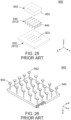
- JPA2015-144159 discloses an assembly 900 of this type.
- the assembly 900 comprises a circuit board structure 910 and a semiconductor element 950, or a device 950.
- the circuit board structure 910 has a circuit board 920 and an interposer 940.
- a positive Z-surface of the circuit board 920 is formed with a plurality of electrical pads 922.
- the interposer 940 has a plurality of contacts 942.
- the device 950 is mounted on the interposer 940 of the circuit board structure 910.
- a negative Z-surface of the device 950 is formed with a plurality of electrical pads 952.
- the interposer 940 electrically connects the electrical pad 952 of the device 950 with the electrical pad 922 of the circuit board 920 via the contact 942.
- the circuit board structure 910 of Patent Document 1 has a drawback that the circuit board structure 910 has an increased size in a Z-direction, or in a height direction.
- the circuit board structure has a main circuit board and a supplemental circuit board.
- the main circuit board has an upper surface and a lower surface in an up-down direction.
- the main circuit board is formed with an accommodating portion.
- the accommodating portion is recessed downward in the up-down direction from the upper surface of the main circuit board.
- the main circuit board has a plurality of upper main conductive portions.
- the upper main conductive portions are formed on the upper surface of the main circuit board.
- the supplemental circuit board has an upper surface and a lower surface in the up-down direction.
- the supplemental circuit board has a plurality of upper supplemental conductive portions.
- the upper supplemental conductive portions are formed on the upper surface of the supplemental circuit board.
- the supplemental circuit board is, at least in part, accommodated in the accommodating portion.
- Each of ones of the connection portions connects a respective one of the upper main conductive portions and a respective one of the upper supplemental conductive portions with each other.
- Another aspect (second aspect) of the present invention provides a harness assembly comprising the assembly of the first aspect, a connector and an electrical wire.
- the assembly further comprises a device which has a device connection portion.
- the device is mounted on the supplemental circuit board.
- the device connection portion is connected with the upper supplemental conductive portion.
- the main circuit board has a front end and a rear end in a front-rear direction perpendicular to the up-down direction.
- the front end of the main circuit board is connected with the connector.
- the rear end of the main circuit board is connected with the electrical wire.
- the assembly of the present invention is configured as follows: the main circuit board is formed with the accommodating portion; the accommodating portion is recessed downward in the up-down direction from the upper surface of the main circuit board; and the supplemental circuit board is, at least in part, accommodated in the accommodating portion. Accordingly, the assembly of the present invention comprises the circuit board structure which has a reduced size in a height direction.
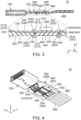
- a harness assembly 10 according to an embodiment of the present invention comprises an assembly 100, a connector 700 and electrical wires 800.
- the connector 700 of the present embodiment is a plug.
- the connector 700 is mateable with a mating connector (not shown), which is positioned forward of the connector 700, from behind the mating connector along a front-rear direction.
- the front-rear direction is an X-direction. Specifically, forward is a positive X-direction while rearward is a negative X-direction.
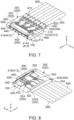
- each of the electrical wires 800 of the present embodiment is two or more. However, the present invention is not limited thereto, but the number of the electrical wire 800 may be one. As shown in Fig. 7 , each of the electrical wires 800 has a center conductor 810 and an outer conductor 820.
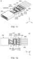
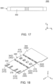
- the assembly 100 of the present embodiment comprises a circuit board structure 200 and a plurality of connection portions 500.
- the circuit board structure 200 of the present embodiment has a main circuit board 300 and a supplemental circuit board 400.
- the main circuit board 300 has a front end 302 and a rear end 304 in the front-rear direction perpendicular to an up-down direction.
- the up-down direction is a Z-direction. Specifically, it is assumed that upward is a positive Z-direction while downward is a negative Z-direction.
- the up-down direction is also referred to as a height direction of the circuit board structure 200.
- the front end 302 of the main circuit board 300 is connected with the connector 700, and the rear end 304 of the main circuit board 300 is connected with any of the electrical wires 800.
- the main circuit board 300 of the present embodiment has a main holding member 305.
- the main holding member 305 is made of resin. It is noted that the main circuit board 300 is not a glass epoxy substrate.
- the main circuit board 300 is formed with an accommodating portion 350.
- the accommodating portion 350 of the present embodiment pierces the main circuit board 300 in the up-down direction.
- the present invention is not limited thereto, but the accommodating portion 350 should be recessed downward in the up-down direction from an upper surface 310 of the main circuit board 300.
- the accommodating portion 350 may have a bottom surface which defines a lower end of the accommodating portion 350 in the up-down direction.
- the accommodating portion 350 has an inner wall surface 352.
- the main circuit board 300 has the upper surface 310 and a lower surface 320 in the up-down direction.
- the upper surface 310 of the present embodiment faces upward in the up-down direction.
- the upper surface 310 is a plane perpendicular to the up-down direction.
- the main circuit board 300 has a plurality of upper main conductive portions 312 which are formed on the upper surface 310.
- the upper main conductive portions 312 of the present embodiment include first upper main conductive portions 3122 and second upper main conductive portions 3124.
- each of the first upper main conductive portions 3122 of the present embodiment is positioned forward of the accommodating portion 350 in the front-rear direction perpendicular to the up-down direction.
- the first upper main conductive portions 3122 include main traces 314 and ground connection portions 316.
- each of the main traces 314 of the present embodiment is a copper wire pattern.
- Each of the main traces 314 is exposed on the upper surface 310 of the main circuit board 300.
- Each of ones of the main traces 314 extends in the front-rear direction on the upper surface 310 and reaches the accommodating portion 350.
- each of the ground connection portions 316 of the present embodiment is exposed on the upper surface 310 of the main circuit board 300.
- Each of the ground connection portions 316 is position around the front end 302 of the main circuit board 300.
- each of the second upper main conductive portions 3124 of the present embodiment is positioned rearward of the accommodating portion 350 in the front-rear direction.
- Each of the second upper main conductive portions 3124 is exposed on the upper surface 310 of the main circuit board 300.
- Each of the second upper main conductive portions 3124 extends in the front-rear direction from the accommodating portion 350 to a rear end of the main holding member 305.
- the lower surface 320 of the present embodiment faces downward in the up-down direction.
- the lower surface 320 is a plane perpendicular to the up-down direction.
- the main circuit board 300 has a plurality of lower main conductive portions 322 which are formed on the lower surface 320 of the main circuit board 300.
- each of the lower main conductive portions 322 of the present embodiment is a copper wire pattern.
- the lower main conductive portions 322 include first lower main conductive portions 3222 and second lower main conductive portions 3224.
- each of the first lower main conductive portions 3222 of the present embodiment is positioned forward of the accommodating portion 350 in the front-rear direction perpendicular to the up-down direction.
- Each of the first lower main conductive portions 3222 is exposed on the lower surface 320 of the main circuit board 300.
- Each of ones of the first lower main conductive portions 3222 extends in the front-rear direction on the lower surface 320 and reaches the accommodating portion 350.
- each of the second lower main conductive portions 3224 of the present embodiment is positioned rearward of the accommodating portions 350 in the front-rear direction.
- Each of the second lower main conductive portions 3224 is exposed on the lower surface 320 of the main circuit board 300.
- Each of the second lower main conductive portions 3224 extends in the front-rear direction from the accommodating portion 350 to the rear end of the main holding member 305.
- the main circuit board 300 further comprises a main inner conductor 340.
- the main inner conductor 340 of the present embodiment is made of metal.
- the main inner conductor 340 has a substantially plate-like shape. As shown in Fig. 3 , a part of the main inner conductor 340 is embedded in the main holding member 305.
- the main inner conductor 340 forms a ground plane and prevents electrical interference between any of the main traces 314 and any of the first lower main conductive portions 3222 and between any of the second upper main conductive portions 3124 and any of the second lower main conductive portions 3224.
- the main inner conductor 340 has a front main inner conductor 343 and a rear main inner conductor 344.
- the front main inner conductor 343 and the rear main inner conductor 344 of the present embodiment are distinct and separated from each other.
- the front main inner conductor 343 defines a front end of the main inner conductor 340 in the front-rear direction.
- the front main inner conductor 343 is positioned forward of the rear main inner conductor 344 in the front-rear direction.
- the front main inner conductor 343 is connected with any of the ground connection portions 316.
- the main inner conductor 340 is connected with ones of the upper main conductive portions 312. It is noted that the front main inner conductor 343 is not connected with any of the main traces 314.
- the rear main inner conductor 344 of the present embodiment defines a rear end of the main inner conductor 340 in the front-rear direction.
- the rear main inner conductor 344 defines the rear end 304 of the main circuit board 300 in the front-rear direction.
- the rear main inner conductor 344 is positioned rearward of the front main inner conductor 343 in the front-rear direction.
- a rear part of the rear main inner conductor 344 is exposed from the main holding member 305.
- the outer conductor 820 of each of the electrical wires 800 is connected with the rear part of the rear main inner conductor 344.
- the main circuit board 300 has main exposed conductive portions 342.
- Each of the main exposed conductive portions 342 is a part of the main inner conductor 340.
- each of the main exposed conductive portions 342 of the present embodiment is exposed on the inner wall surface 352 of the accommodating portion 350.
- Each of the main exposed conductive portions 342 is exposed from the main holding member 305.
- the main exposed conductive portion 342 has a resilient property. In other words, the main exposed conductive portion 342 is configured to be resiliently deformable.
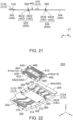
- the main exposed conductive portion 342 is connected with the ground connection portion 316. In other words, the main exposed conductive portion 342 is connected with the upper main conductive portion 312. Referring to Fig. 22 , the main exposed conductive portion 342 is not connected with the upper main conductive portion 312 on the inner wall surface 352 of the accommodating portion 350.
- the main exposed conductive portions 342 include front main exposed conductive portions 3422 and rear main exposed conductive portions 3424.
- each of the front main exposed conductive portions 3422 of the present embodiment is provided at the front main inner conductor 343. More specifically, each of the front main exposed conductive portions 3422 is provided at a rear end of the front main inner conductor 343. Each of the front main exposed conductive portions 3422 is connected with any of the ground connection portions 316.
- each of the rear main exposed conductive portions 3424 of the present embodiment is provided at the rear main inner conductor 344. More specifically, each of the rear main exposed conductive portions 3424 is provided at a front end of the rear main inner conductor 344.
- the main circuit board 300 has regulating portions 360.
- each of the regulating portions 360 of the present embodiment is recessed outward in a right-left direction.
- Each of the regulating portions 360 communicates with the accommodating portion 350 in the right-left direction.
- the right-left direction is a Y-direction.
- Each of the regulating portions 360 opens upward in the up-down direction.
- the supplemental circuit board 400 of the present embodiment is distinct and separated from the main circuit board 300.
- the supplemental circuit board 400 has a supplemental holding member 405.
- the supplemental holding member 405 is made of resin. It is noted that the supplemental circuit board 400 is not a glass epoxy substrate.
- the supplemental circuit board 400 of the present embodiment is completely accommodated in the accommodating portion 350.
- the supplemental circuit board 400 does not protrude in the up-down direction from the main circuit board 300 when the supplemental circuit board 400 is accommodated in the accommodating portion 350.
- the present invention is not limited thereto, but the supplemental circuit board 400 should be, at least in part, accommodated in the accommodating portion 350.
- the circuit board structure 200 of the present embodiment has a reduced size in the height direction.
- the supplemental circuit board 400 has an upper surface 410 and a lower surface 420 in the up-down direction.
- the upper surface 410 of the present embodiment faces upward in the up-down direction.
- the upper surface 410 is a plane perpendicular to the up-down direction.
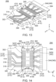
- the supplemental circuit board 400 has a plurality of upper supplemental conductive portions 412 which are formed on the upper surface 410.
- the upper supplemental conductive portions 412 of the present embodiment include supplemental traces 414 and connected portions 416.
- each of the supplemental traces 414 of the present embodiment is exposed on the upper surface 410 of the supplemental circuit board 400.
- the supplemental traces 414 include front supplemental traces 4142 and rear supplemental traces 4144.
- each of the front supplemental traces 4142 of the present embodiment extends in the front-rear direction and reaches a front end of the supplemental circuit board 400.
- Each of the front supplemental traces 4142 is positioned forward of any of the rear supplemental traces 4144 in the front-rear direction.
- each of the rear supplemental traces 4144 of the present embodiment extends in the front-rear direction and reaches a rear end of the supplemental circuit board 400.
- Each of the rear supplemental traces 4144 is positioned rearward of any of the front supplemental traces 4142 in the front-rear direction.
- each of the connected portions 416 of the present embodiment is exposed on the upper surface 410 of the supplemental circuit board 400.
- Each of the connected portions 416 is positioned at a middle of the supplemental circuit board 400 in the front-rear direction.
- Each of the connected portions 416 is positioned between any of the front supplemental traces 4142 and any of the rear supplemental traces 4144 in the front-rear direction.
- the lower surface 420 of the present embodiment faces downward in the up-down direction.
- the lower surface 420 is a plane perpendicular to the up-down direction.
- the supplemental circuit board 400 has a plurality of lower supplemental conductive portions 422 which are formed on the lower surface 420. Each of the lower supplemental conductive portions 422 is exposed on the lower surface 420 of the supplemental circuit board 400.
- the supplemental circuit board 400 has side surfaces 430 in a direction perpendicular to the up-down direction.
- each of the side surfaces 430 of the present embodiment defines an end portion of the supplemental circuit board 400 in the front-rear direction. More specifically, the supplemental circuit board 400 has two of the side surfaces 430. One of the side surfaces 430 is a front surface of the supplemental circuit board 400, and a remaining one of the side surfaces 430 is a rear surface of the supplemental circuit board 400.
- the supplemental circuit board 400 further comprises a supplemental inner conductor 440.
- the supplemental inner conductor 440 of the present embodiment is made of metal.
- the supplemental inner conductor 440 has a substantially plate-like shape.
- the supplemental inner conductor 440 forms a ground plane and prevents electrical interference between any of the supplemental traces 414 and any of the lower supplemental conductive portions 422.
- Each of the connected portions 416 is connected with the supplemental inner conductor 440.
- the supplemental inner conductor 440 is connected with ones of the upper supplemental conductive portions 412. It is noted that none of the supplemental traces 414 are connected with the supplemental inner conductor 440.
- a part of the supplemental inner conductor 440 is embedded in the supplemental holding member 405.
- the supplemental inner conductor 440 is positioned between the front main inner conductor 343 and the rear main inner conductor 344 in the front-rear direction when the supplemental circuit board 400 is accommodated in the accommodating portion 350.
- the front main inner conductor 343 is positioned forward of the supplemental inner conductor 440 in the front-rear direction when the supplemental circuit board 400 is accommodated in the accommodating portion 350.
- the rear main inner conductor 344 is positioned rearward of the supplemental inner conductor 440 in the front-rear direction when the supplemental circuit board 400 is accommodated in the accommodating portion 350.
- the supplemental circuit board 400 has supplemental exposed conductive portions 432, 442.
- the supplemental exposed conductive portions 432, 442 of the present embodiment are exposed on the side surfaces 430.
- the supplemental exposed conductive portion 432 is also referred to as a side connection portion 432.
- the supplemental exposed conductive portion 442 is also referred to as a supplemental inner conductor exposed portion 442.
- the side connection portions 432 of the present embodiment are provided on the side surfaces 430 of the supplemental circuit board 400.
- the side connection portion 432 is connected with the supplemental trace 414 on the side surface 430 of the supplemental circuit board 400.
- the supplemental exposed conductive portion 432 is connected with the upper supplemental conductive portion 412 on the side surface 430 of the supplemental circuit board 400.
- each of the side connection portions 432 extends from the upper surface 410 of the supplemental circuit board 400 to the lower surface 420 of the supplemental circuit board 400.
- Each of ones of the lower supplemental conductive portions 422 is connected with a respective one of the supplemental traces 414 by a respective one of the side connection portions 432.
- each of the ones of the lower supplemental conductive portions 422 is connected with a respective one of the upper supplemental conductive portions 412 by the respective one of the side connection portions 432.
- the supplemental circuit board 400 is not a glass epoxy substrate, the part of the supplemental inner conductor 440 is embedded in the supplemental holding member 405 made of resin, and the supplemental circuit board 400 is provided with the side connection portions 432 each of which connects the upper supplemental conductive portion 412 with the lower supplemental conductive portion 422.
- a portion equivalent to the side connection portion 432 cannot be formed on a side surface of the glass epoxy substrate.
- the glass epoxy substrate is formed with, instead of the side connection portion 432, a via hole which connects the upper supplemental conductive portion 412 with the lower supplemental conductive portion 422.
- the inner layer which corresponds to the supplemental inner conductor 440, must be formed so as to be away from and in no contact with the via hole.
- the inner layer in this case has a drawback of lack of shielding between the supplemental trace 414 and the lower supplemental conductive portion 422 at a location where the inner layer is away from and in no contact with the via hole.
- the supplemental circuit board 400 of the present embodiment is configured so that the side connection portions 432, each of which connects the upper supplemental conductive portion 412 with the lower supplemental conductive portion 422, are provided on the side surfaces 430. Accordingly, the supplemental circuit board 400 of the present embodiment does not have the drawback of the lack of shielding as described above. Specifically, in the supplemental circuit board 400 of the present embodiment, the supplemental inner conductor 440 can provide full shielding between any of the supplemental traces 414 and any of the lower supplemental conductive portions 422, and thereby the supplemental inner conductor 440 provides an increased shielding effect.
- main circuit board 300 of the present embodiment also has the same effect as the effect of the supplemental circuit board 400 as described above.
- each of the supplemental inner conductor exposed portions 442 of the present embodiment is a part of the supplemental inner conductor 440.
- each of the supplemental exposed conductive portions 442 is the part of the supplemental inner conductor 440.
- Each of the supplemental inner conductor exposed portions 442 is connected with any of the connected portions 416.
- the supplemental exposed conductive portion 442 is connected with the upper supplemental conductive portions 412.
- the main exposed conductive portion 342 and the supplemental inner conductor exposed portion 442 are in contact with each other when the supplemental circuit board 400 is accommodated in the accommodating portion 350.
- the main exposed conductive portion 342 is connected with the supplemental inner conductor exposed portion 442 when the supplemental circuit board 400 is accommodated in the accommodating portion 350.
- the main exposed conductive portion 342 is connected with the supplemental exposed conductive portion 442 when the supplemental circuit board 400 is accommodated in the accommodating portion 350.
- the supplemental inner conductor exposed portion 442 is not configured so as to be resiliently deformable.
- the circuit board structure 200 of the present embodiment is configured so that the main exposed conductive portion 342 has the resilient property as described above, the present invention is not limited thereto.
- the supplemental inner conductor exposed portion 442 may have a resilient property.
- at least one of the main exposed conductive portion 342 and the supplemental exposed conductive portion 442 should have a resilient property. This can ensure a stable connection of the main exposed conductive portion 342 with the supplemental exposed conductive portion 442 when the supplemental circuit board 400 is accommodated in the accommodating portion 350.
- the supplemental inner conductor exposed portions 442 include front supplemental inner conductor exposed portions 4422 and rear supplemental inner conductor exposed portions 4424.
- the front supplemental inner conductor exposed portion 4422 of the present embodiment defines the front end of the supplemental circuit board 400 in the front-rear direction.
- Each of the front supplemental inner conductor exposed portions 4422 is positioned forward of any of the rear supplemental inner conductor exposed portions 4424 in the front-rear direction.
- Each of the front supplemental inner conductor exposed portions 4422 is positioned forward of any of the connected portions 416 in the front-rear direction.
- the front supplemental inner conductor exposed portion 4422 is connected with the front main exposed conductive portion 3422 when the supplemental circuit board 400 is accommodated in the accommodating portion 350.
- the rear supplemental inner conductor exposed portion 4424 of the present embodiment defines the rear end of the supplemental circuit board 400 in the front-rear direction.
- Each of the rear supplemental inner conductor exposed portions 4424 is positioned rearward of any of the front supplemental inner conductor exposed portions 4422 in the front-rear direction.
- Each of the rear supplemental inner conductor exposed portions 4424 is positioned rearward of any of the connected portions 416 in the front-rear direction.
- the rear supplemental inner conductor exposed portion 4424 is connected with the rear main exposed conductive portion 3424 when the supplemental circuit board 400 is accommodated in the accommodating portion 350.
- the supplemental circuit board 400 has regulated portions 460.
- each of the regulated portions 460 of the present embodiment protrudes outward in the right-left direction.
- the regulated portions 460 correspond to the regulating portions 360, respectively.
- each of the regulated portions 460 is accommodated in the corresponding regulating portion 360 when the supplemental circuit board 400 is accommodated in the accommodating portion 350. This prevents deviation of the supplemental circuit board 400 with respect to the main circuit board 300 in a perpendicular plane perpendicular to the up-down direction when the supplemental circuit board 400 is accommodated in the accommodating portion 350.
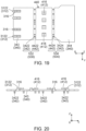
- connection portions 500 of the present embodiment include first connection portions 510, second connection portions 520 and third connection portions 530.
- each of the first connection portions 510 of the present embodiment is distinct and separated from the circuit board structure 200. More specifically, each of the first connection portions 510 is a chip capacitor or zero-ohm resistor.
- the first connection portions 510 include first upper connection portions 512 and first lower connection portions 514.
- each of the first upper connection portions 512 of the present embodiment is positioned on the upper surface 310 of the main circuit board 300.
- Each of the first upper connection portions 512 is positioned on the upper surface 410 of the supplemental circuit board 400.
- the first upper connection portion 512 connects the main trace 314 of the first upper main conductive portion 3122 and the front supplemental trace 4142 of the supplemental trace 414 of the upper supplemental conductive portion 412 with each other.
- each of the first lower connection portions 514 of the present embodiment is positioned on the lower surface 320 of the main circuit board 300.
- Each of the first lower connection portions 514 is positioned on the lower surface 420 of the supplemental circuit board 400.
- the first lower connection portion 514 connects the first lower main conductive portion 3222 and the lower supplemental conductive portion 422 with each other.
- each of the second connection portions 520 of the present embodiment is distinct and separated from the circuit board structure 200. More specifically, each of the second connection portions 520 is a chip capacitor or zero-ohm resistor.
- each of the first connection portions 510 and the second connection portions 520 is distinct and separated from the circuit board structure 200.
- each of ones of the connection portions 500 is distinct and separated from the circuit board structure 200.
- the second connection portions 520 include second upper connection portions 522 and second lower connection portions 524.
- each of the second upper connection portions 522 of the present embodiment is positioned on the upper surface 310 of the main circuit board 300.
- Each of the second upper connection portions 522 is positioned on the upper surface 410 of the supplemental circuit board 400.
- the second upper connection portion 522 connects the rear supplemental trace 4144 of the supplemental trace 414 of the upper supplemental conductive portion 412 and the second upper main conductive portion 3124 with each other.
- each of the second lower connection portions 524 of the present embodiment is positioned on the lower surface 320 of the main circuit board 300.
- Each of the second lower connection portions 524 is positioned on the lower surface 420 of the supplemental circuit board 400.
- the second lower connection portion 524 connects the lower supplemental conductive portion 422 and the second lower main conductive portion 3224 with each other.
- the first lower connection portion 514 connects the first lower main conductive portion 3222 and the lower supplemental conductive portion 422 with each other
- the second lower connection portion 524 connects the lower supplemental conductive portion 422 and the second lower main conductive portion 3224 with each other.
- each of ones of the connection portions 500 connects a respective one of the lower main conductive portions 322 and a respective one of the lower supplemental conductive portions 422 with each other.
- the third connection portions 530 of the present embodiment include third front connection portions 532 and third rear connection portions 534.
- each of the third front connection portions 532 of the present embodiment consists of the front main exposed conductive portion 3422 and the front supplemental inner conductor exposed portion 4422.
- the front main inner conductor 343 and the supplemental inner conductor 440 are connected with each other via any of the third front connection portions 532.
- the ground connection portion 316 is connected with the front main inner conductor 343, and the connected portion 416 is connected with the supplemental inner conductor 440.
- the third front connection portion 532 connects the ground connection portion 316 and the connected portion 416 with each other.
- the first upper connection portion 512 connects the main trace 314 and the front supplemental trace 4142 with each other
- the second upper connection portion 522 connects the rear supplemental trace 4144 and the second upper main conductive portion 3124 with each other
- the third front connection portion 532 connects the ground connection portion 316 and the connected portion 416 with each other.
- each of ones of the connection portions 500 connects a respective one of the upper main conductive portions 312 and a respective one of the upper supplemental conductive portions 412 with each other.
- each of the third rear connection portions 534 of the present embodiment consists of the rear supplemental inner conductor exposed portion 4424 and the rear main exposed conductive portion 3424.
- the supplemental inner conductor 440 and the rear main inner conductor 344 are connected with each other via any of the third rear connection portions 534.
- the assembly 100 further comprises a device 600.
- the device 600 of the present embodiment is a semiconductor element.
- the device 600 is mounted on the supplemental circuit board 400.
- the device 600 has device connection portions 610.
- the device connection portion 610 is connected with the upper supplemental conductive portion 412. More specifically, referring to Figs. 6 and 14 , each of ones of the device connection portions 610 is connected with a respective one of the supplemental traces 414. In addition, each of remaining ones of the device connection portions 610 is connected with a respective one of the connected portions 416. Since each of the connected portions 416 is connected with the supplemental inner conductor 440 as described above, the device 600 is connected with the supplemental inner conductor 440 via the device connection portions 610 and the connected portions 416. Thus, the device 600 can use the supplemental inner conductor 440 as a heat sink which draws heat away from the device 600.
- the device 600 connects the front supplemental trace 4142 and the rear supplemental trace 4144 with each other.
- the first upper connection portion 512 connects the main trace 314 and the front supplemental trace 4142 with each other
- the device 600 connects the front supplemental trace 4142 and the rear supplemental trace 4144 with each other
- the second upper connection portion 522 connects the rear supplemental trace 4144 and the second upper main conductive portion 3124 with each other.
- the first upper main conductive portion 3122 is connected with the second upper main conductive portion 3124 via the upper supplemental conductive portions 412, the device 600 and ones of the connection portions 500.
- the main circuit board 300 of the present embodiment is configured so that the main exposed conductive portion 342 is not connected with the upper main conductive portion 312 on the inner wall surface 352 of the accommodating portion 350, the present invention is not limited thereto. Specifically, the main exposed conductive portion 342 may be connected with the upper main conductive portion 312 on the inner wall surface 352 of the accommodating portion 350.
- the assembly 100 of the present embodiment comprises the device 600
- the present invention is not limited thereto, but the assembly 100 may comprise no device 600.
- the upper surface 410 of the supplemental circuit board 400 is formed with no connected portion 416, but formed only with the supplemental traces 414.
- the front supplemental trace 4142 and the rear supplemental trace 4144 are directly connected with each other in this case. Accordingly, if the assembly 100 comprises no device 600, the first upper main conductive portion 3122 should be connected with the second upper main conductive portion 3124 via the upper supplemental conductive portion 412 and ones of the connection portions 500.
- the harness assembly 10 of the present embodiment comprises the assembly 100, the connector 700 and the electrical wires 800
- the present invention is not limited thereto.
- the harness assembly 10 may comprises no connector 700.
- the harness assembly 10 may comprise only a set of the assembly 100 and the electrical wires 800.
- the front end 302 of the main circuit board 300 of the assembly 100 functions as a card edge connector.
- a first aspect of the invention is an assembly comprising a circuit board structure and a plurality of connection portions, wherein:
- a second aspect of the invention is the assembly as recited in the first aspect, wherein:
- a third aspect of the invention is the assembly as recited in the second aspect, wherein:
- a fourth aspect of the invention is the assembly as recited in the first or second aspect, wherein:
- a fifth aspect of the invention is the assembly as recited in the fourth aspect, wherein the supplemental exposed conductive portion is connected with the upper supplemental conductive portion on the side surface of the supplemental circuit board.
- a sixth aspect of the invention is the assembly as recited in the fourth aspect, wherein:
- a seventh aspect of the invention is The assembly as recited in one of the fourth to sixth aspects, wherein at least one of the main exposed conductive portion and the supplemental exposed conductive portion has a resilient property.
- a eighth aspect of the invention is the assembly as recited in one of the first to seventh aspects, wherein each of ones of the connection portions is distinct and separated from the circuit board structure.
- a ninth aspect of the invention is the assembly as recited in one of the first to eighth aspects, wherein:
- a tenth aspect of the invention is the assembly as recited in one of the first to nineth aspects, wherein:
- a eleventh aspect of the invention is a harness assembly comprising the assembly as recited in the tenth aspect, a connector and an electrical wire, wherein:
Landscapes
- Engineering & Computer Science (AREA)
- Microelectronics & Electronic Packaging (AREA)
- Coupling Device And Connection With Printed Circuit (AREA)
- Multi-Conductor Connections (AREA)
- Combinations Of Printed Boards (AREA)
Applications Claiming Priority (2)
| Application Number | Priority Date | Filing Date | Title |
|---|---|---|---|
| JP2021199893A JP7779719B2 (ja) | 2021-12-09 | 2021-12-09 | 組立体及びハーネス組立体 |
| EP22204403.4A EP4207954B1 (de) | 2021-12-09 | 2022-10-28 | Anordnung und kabelbaumanordnung |
Related Parent Applications (2)
| Application Number | Title | Priority Date | Filing Date |
|---|---|---|---|
| EP22204403.4A Division EP4207954B1 (de) | 2021-12-09 | 2022-10-28 | Anordnung und kabelbaumanordnung |
| EP22204403.4A Division-Into EP4207954B1 (de) | 2021-12-09 | 2022-10-28 | Anordnung und kabelbaumanordnung |
Publications (3)
| Publication Number | Publication Date |
|---|---|
| EP4465453A2 true EP4465453A2 (de) | 2024-11-20 |
| EP4465453A3 EP4465453A3 (de) | 2025-03-05 |
| EP4465453B1 EP4465453B1 (de) | 2026-03-25 |
Family
ID=84044579
Family Applications (2)
| Application Number | Title | Priority Date | Filing Date |
|---|---|---|---|
| EP24202484.2A Active EP4465453B1 (de) | 2021-12-09 | 2022-10-28 | Kabelbaumanordnung |
| EP22204403.4A Active EP4207954B1 (de) | 2021-12-09 | 2022-10-28 | Anordnung und kabelbaumanordnung |
Family Applications After (1)
| Application Number | Title | Priority Date | Filing Date |
|---|---|---|---|
| EP22204403.4A Active EP4207954B1 (de) | 2021-12-09 | 2022-10-28 | Anordnung und kabelbaumanordnung |
Country Status (4)
| Country | Link |
|---|---|
| US (1) | US12482973B2 (de) |
| EP (2) | EP4465453B1 (de) |
| JP (1) | JP7779719B2 (de) |
| CN (1) | CN116261254A (de) |
Families Citing this family (1)
| Publication number | Priority date | Publication date | Assignee | Title |
|---|---|---|---|---|
| JP7363551B2 (ja) * | 2020-02-12 | 2023-10-18 | 住友電気工業株式会社 | コネクタ付き多心ケーブル |
Citations (1)
| Publication number | Priority date | Publication date | Assignee | Title |
|---|---|---|---|---|
| JP2015144159A (ja) | 2014-01-31 | 2015-08-06 | 日本航空電子工業株式会社 | 中継部材及び中継部材の製造方法 |
Family Cites Families (14)
| Publication number | Priority date | Publication date | Assignee | Title |
|---|---|---|---|---|
| JPS60106362U (ja) * | 1983-12-23 | 1985-07-19 | パイオニア株式会社 | 回路基板 |
| JPH0412714Y2 (de) | 1984-10-09 | 1992-03-26 | ||
| JPH05327272A (ja) | 1992-05-21 | 1993-12-10 | Matsushita Electric Ind Co Ltd | 電子回路装置 |
| US5661336A (en) * | 1994-05-03 | 1997-08-26 | Phelps, Jr.; Douglas Wallace | Tape application platform and processes therefor |
| JP3501079B2 (ja) | 2000-03-10 | 2004-02-23 | 住友電装株式会社 | ジャンクションボックスに収容する回路体 |
| AU2008247315B2 (en) | 2007-05-03 | 2011-11-03 | Coolon Pty Ltd | System of connecting printed circuit boards 'COOLLOCK' |
| US7767494B2 (en) * | 2008-06-30 | 2010-08-03 | Headway Technologies, Inc. | Method of manufacturing layered chip package |
| CN103517542A (zh) * | 2012-06-14 | 2014-01-15 | 欧司朗股份有限公司 | 电路板、具有该电路板的电子模块、照明装置和制造该电路板的方法 |
| US9525227B2 (en) * | 2012-07-21 | 2016-12-20 | Foxconn Interconnect Technology Limited | Flippable electrical connector |
| JP6221132B2 (ja) * | 2013-03-07 | 2017-11-01 | 矢崎総業株式会社 | プリント配線板 |
| TWI665828B (zh) | 2017-09-12 | 2019-07-11 | 巧連科技股份有限公司 | 板對板連接器 |
| CN110137726B (zh) * | 2018-02-09 | 2022-08-19 | 富士康(昆山)电脑接插件有限公司 | 线缆连接器组件 |
| DE102018111554A1 (de) * | 2018-05-15 | 2019-11-21 | HELLA GmbH & Co. KGaA | Leiterplattenaufbau zur Aufnahme wenigstens eines Halbleiterleuchtmittels |
| WO2020074997A1 (en) | 2018-10-09 | 2020-04-16 | 3M Innovative Properties Company | Connector assembly having low profile |
-
2021
- 2021-12-09 JP JP2021199893A patent/JP7779719B2/ja active Active
-
2022
- 2022-10-21 US US17/971,472 patent/US12482973B2/en active Active
- 2022-10-27 CN CN202211330670.0A patent/CN116261254A/zh active Pending
- 2022-10-28 EP EP24202484.2A patent/EP4465453B1/de active Active
- 2022-10-28 EP EP22204403.4A patent/EP4207954B1/de active Active
Patent Citations (1)
| Publication number | Priority date | Publication date | Assignee | Title |
|---|---|---|---|---|
| JP2015144159A (ja) | 2014-01-31 | 2015-08-06 | 日本航空電子工業株式会社 | 中継部材及び中継部材の製造方法 |
Also Published As
| Publication number | Publication date |
|---|---|
| US12482973B2 (en) | 2025-11-25 |
| US20230187865A1 (en) | 2023-06-15 |
| JP7779719B2 (ja) | 2025-12-03 |
| EP4207954A2 (de) | 2023-07-05 |
| CN116261254A (zh) | 2023-06-13 |
| JP2023085706A (ja) | 2023-06-21 |
| EP4207954B1 (de) | 2025-12-10 |
| EP4465453B1 (de) | 2026-03-25 |
| EP4207954A3 (de) | 2023-10-11 |
| EP4465453A3 (de) | 2025-03-05 |
Similar Documents
| Publication | Publication Date | Title |
|---|---|---|
| US8215995B1 (en) | Connector attached to a bracket and mounted in a cutout in a substrate | |
| US8062041B2 (en) | Connector | |
| EP2285195A1 (de) | Buchse, Schalttafelanordnung und Vorrichtung damit | |
| US8007327B2 (en) | Electrical connector having positioning posts defined on insulative base | |
| US11469558B2 (en) | Connector and electronic equipment | |
| CN105098529B (zh) | 插座电连接器 | |
| US11984689B2 (en) | Conductive housing for connector and connector comprising the same | |
| JP2004247283A (ja) | 周辺部がシールされる高密度マルチピンコネクタ | |
| EP4465453B1 (de) | Kabelbaumanordnung | |
| US9214747B2 (en) | Low profile electrical connector have a FPC | |
| US7692281B2 (en) | Land grid array module with contact locating features | |
| US7367814B2 (en) | Electrical contacts used in an electrical connector | |
| KR101821420B1 (ko) | 소켓 | |
| CN104319509A (zh) | 板连接器 | |
| US7775803B2 (en) | Electrical connector having contact retention device | |
| US7445460B1 (en) | Electrical connector with contact fall-out preventing arrangement | |
| JPH11297435A (ja) | コネクタ装置、コネクタ装置を有する回路モジュールおよび回路モジュールを搭載した電子機器 | |
| US20100081333A1 (en) | Electrical connector confitured by upper and lower units | |
| JP2019200872A (ja) | コネクタ | |
| US11056844B2 (en) | Connector, device provided with the same and method of manufacturing the same | |
| CN103208707B (zh) | 电连接器 | |
| TWI824327B (zh) | 電子元件 | |
| CN111342251B (zh) | 插座组件的电力供给 | |
| US5352124A (en) | Socket for IC package | |
| US20020039285A1 (en) | Device for reducing electromagnetic interference in a processor assembly |
Legal Events
| Date | Code | Title | Description |
|---|---|---|---|
| PUAI | Public reference made under article 153(3) epc to a published international application that has entered the european phase |
Free format text: ORIGINAL CODE: 0009012 |
|
| STAA | Information on the status of an ep patent application or granted ep patent |
Free format text: STATUS: THE APPLICATION HAS BEEN PUBLISHED |
|
| AC | Divisional application: reference to earlier application |
Ref document number: 4207954 Country of ref document: EP Kind code of ref document: P |
|
| AK | Designated contracting states |
Kind code of ref document: A2 Designated state(s): AL AT BE BG CH CY CZ DE DK EE ES FI FR GB GR HR HU IE IS IT LI LT LU LV MC ME MK MT NL NO PL PT RO RS SE SI SK SM TR |
|
| REG | Reference to a national code |
Ref country code: DE Ref legal event code: R079 Free format text: PREVIOUS MAIN CLASS: H01R0012720000 Ipc: H05K0001140000 Ref document number: 602022033242 Country of ref document: DE |
|
| PUAL | Search report despatched |
Free format text: ORIGINAL CODE: 0009013 |
|
| AK | Designated contracting states |
Kind code of ref document: A3 Designated state(s): AL AT BE BG CH CY CZ DE DK EE ES FI FR GB GR HR HU IE IS IT LI LT LU LV MC ME MK MT NL NO PL PT RO RS SE SI SK SM TR |
|
| RIC1 | Information provided on ipc code assigned before grant |
Ipc: H01R 24/60 20110101ALN20250128BHEP Ipc: H01L 23/498 20060101ALN20250128BHEP Ipc: H01L 23/13 20060101ALN20250128BHEP Ipc: H05K 1/11 20060101ALN20250128BHEP Ipc: H01R 12/72 20110101ALI20250128BHEP Ipc: H05K 1/14 20060101AFI20250128BHEP |
|
| STAA | Information on the status of an ep patent application or granted ep patent |
Free format text: STATUS: REQUEST FOR EXAMINATION WAS MADE |
|
| 17P | Request for examination filed |
Effective date: 20250723 |
|
| GRAP | Despatch of communication of intention to grant a patent |
Free format text: ORIGINAL CODE: EPIDOSNIGR1 |
|
| STAA | Information on the status of an ep patent application or granted ep patent |
Free format text: STATUS: GRANT OF PATENT IS INTENDED |
|
| RIC1 | Information provided on ipc code assigned before grant |
Ipc: H05K 1/14 20060101AFI20250924BHEP Ipc: H01R 12/72 20110101ALI20250924BHEP Ipc: H05K 1/11 20060101ALN20250924BHEP Ipc: H01L 23/13 20060101ALN20250924BHEP Ipc: H01L 23/498 20060101ALN20250924BHEP |
|
| RIC1 | Information provided on ipc code assigned before grant |
Ipc: H05K 1/14 20060101AFI20251007BHEP Ipc: H01R 12/72 20110101ALI20251007BHEP Ipc: H05K 1/11 20060101ALN20251007BHEP Ipc: H01L 23/13 20060101ALN20251007BHEP Ipc: H01L 23/498 20060101ALN20251007BHEP |
|
| INTG | Intention to grant announced |
Effective date: 20251028 |
|
| GRAS | Grant fee paid |
Free format text: ORIGINAL CODE: EPIDOSNIGR3 |
|
| GRAA | (expected) grant |
Free format text: ORIGINAL CODE: 0009210 |
|
| STAA | Information on the status of an ep patent application or granted ep patent |
Free format text: STATUS: THE PATENT HAS BEEN GRANTED |
|
| AC | Divisional application: reference to earlier application |
Ref document number: 4207954 Country of ref document: EP Kind code of ref document: P |
|
| AK | Designated contracting states |
Kind code of ref document: B1 Designated state(s): AL AT BE BG CH CY CZ DE DK EE ES FI FR GB GR HR HU IE IS IT LI LT LU LV MC ME MK MT NL NO PL PT RO RS SE SI SK SM TR |
|
| REG | Reference to a national code |
Ref country code: CH Ref legal event code: F10 Free format text: ST27 STATUS EVENT CODE: U-0-0-F10-F00 (AS PROVIDED BY THE NATIONAL OFFICE) Effective date: 20260325 Ref country code: GB Ref legal event code: FG4D |
|
| REG | Reference to a national code |
Ref country code: DE Ref legal event code: R096 Ref document number: 602022033242 Country of ref document: DE |
|
| REG | Reference to a national code |
Ref country code: IE Ref legal event code: FG4D |
|
| PG25 | Lapsed in a contracting state [announced via postgrant information from national office to epo] |
Ref country code: RS Free format text: LAPSE BECAUSE OF FAILURE TO SUBMIT A TRANSLATION OF THE DESCRIPTION OR TO PAY THE FEE WITHIN THE PRESCRIBED TIME-LIMIT Effective date: 20260625 |
|
| PG25 | Lapsed in a contracting state [announced via postgrant information from national office to epo] |
Ref country code: GR Free format text: LAPSE BECAUSE OF FAILURE TO SUBMIT A TRANSLATION OF THE DESCRIPTION OR TO PAY THE FEE WITHIN THE PRESCRIBED TIME-LIMIT Effective date: 20260626 |
|
| REG | Reference to a national code |
Ref country code: LT Ref legal event code: MG9D |
|
| PG25 | Lapsed in a contracting state [announced via postgrant information from national office to epo] |
Ref country code: LT Free format text: LAPSE BECAUSE OF FAILURE TO SUBMIT A TRANSLATION OF THE DESCRIPTION OR TO PAY THE FEE WITHIN THE PRESCRIBED TIME-LIMIT Effective date: 20260325 |
|
| PG25 | Lapsed in a contracting state [announced via postgrant information from national office to epo] |
Ref country code: NO Free format text: LAPSE BECAUSE OF FAILURE TO SUBMIT A TRANSLATION OF THE DESCRIPTION OR TO PAY THE FEE WITHIN THE PRESCRIBED TIME-LIMIT Effective date: 20260625 |
|
| PG25 | Lapsed in a contracting state [announced via postgrant information from national office to epo] |
Ref country code: FI Free format text: LAPSE BECAUSE OF FAILURE TO SUBMIT A TRANSLATION OF THE DESCRIPTION OR TO PAY THE FEE WITHIN THE PRESCRIBED TIME-LIMIT Effective date: 20260325 Ref country code: SE Free format text: LAPSE BECAUSE OF FAILURE TO SUBMIT A TRANSLATION OF THE DESCRIPTION OR TO PAY THE FEE WITHIN THE PRESCRIBED TIME-LIMIT Effective date: 20260325 |
|
| PG25 | Lapsed in a contracting state [announced via postgrant information from national office to epo] |
Ref country code: HR Free format text: LAPSE BECAUSE OF FAILURE TO SUBMIT A TRANSLATION OF THE DESCRIPTION OR TO PAY THE FEE WITHIN THE PRESCRIBED TIME-LIMIT Effective date: 20260325 |
|
| PG25 | Lapsed in a contracting state [announced via postgrant information from national office to epo] |
Ref country code: LV Free format text: LAPSE BECAUSE OF FAILURE TO SUBMIT A TRANSLATION OF THE DESCRIPTION OR TO PAY THE FEE WITHIN THE PRESCRIBED TIME-LIMIT Effective date: 20260325 |
|
| PG25 | Lapsed in a contracting state [announced via postgrant information from national office to epo] |
Ref country code: BG Free format text: LAPSE BECAUSE OF FAILURE TO SUBMIT A TRANSLATION OF THE DESCRIPTION OR TO PAY THE FEE WITHIN THE PRESCRIBED TIME-LIMIT Effective date: 20260325 |
|
| REG | Reference to a national code |
Ref country code: NL Ref legal event code: MP Effective date: 20260325 |