EP4451338A1 - Schottkydiode mit vergrabener doppelsperrschicht-gitter und verfahren zu deren herstellung - Google Patents
Schottkydiode mit vergrabener doppelsperrschicht-gitter und verfahren zu deren herstellung Download PDFInfo
- Publication number
- EP4451338A1 EP4451338A1 EP23201908.3A EP23201908A EP4451338A1 EP 4451338 A1 EP4451338 A1 EP 4451338A1 EP 23201908 A EP23201908 A EP 23201908A EP 4451338 A1 EP4451338 A1 EP 4451338A1
- Authority
- EP
- European Patent Office
- Prior art keywords
- layer
- grid
- schottky
- material layer
- schottky material
- Prior art date
- Legal status (The legal status is an assumption and is not a legal conclusion. Google has not performed a legal analysis and makes no representation as to the accuracy of the status listed.)
- Pending
Links
Images


Classifications
-
- H—ELECTRICITY
- H10—SEMICONDUCTOR DEVICES; ELECTRIC SOLID-STATE DEVICES NOT OTHERWISE PROVIDED FOR
- H10D—INORGANIC ELECTRIC SEMICONDUCTOR DEVICES
- H10D8/00—Diodes
- H10D8/60—Schottky-barrier diodes
-
- H—ELECTRICITY
- H10—SEMICONDUCTOR DEVICES; ELECTRIC SOLID-STATE DEVICES NOT OTHERWISE PROVIDED FOR
- H10D—INORGANIC ELECTRIC SEMICONDUCTOR DEVICES
- H10D62/00—Semiconductor bodies, or regions thereof, of devices having potential barriers
- H10D62/10—Shapes, relative sizes or dispositions of the regions of the semiconductor bodies; Shapes of the semiconductor bodies
- H10D62/102—Constructional design considerations for preventing surface leakage or controlling electric field concentration
- H10D62/103—Constructional design considerations for preventing surface leakage or controlling electric field concentration for increasing or controlling the breakdown voltage of reverse-biased devices
- H10D62/105—Constructional design considerations for preventing surface leakage or controlling electric field concentration for increasing or controlling the breakdown voltage of reverse-biased devices by having particular doping profiles, shapes or arrangements of PN junctions; by having supplementary regions, e.g. junction termination extension [JTE]
- H10D62/106—Constructional design considerations for preventing surface leakage or controlling electric field concentration for increasing or controlling the breakdown voltage of reverse-biased devices by having particular doping profiles, shapes or arrangements of PN junctions; by having supplementary regions, e.g. junction termination extension [JTE] having supplementary regions doped oppositely to or in rectifying contact with regions of the semiconductor bodies, e.g. guard rings with PN or Schottky junctions
- H10D62/107—Buried supplementary regions, e.g. buried guard rings
-
- H—ELECTRICITY
- H10—SEMICONDUCTOR DEVICES; ELECTRIC SOLID-STATE DEVICES NOT OTHERWISE PROVIDED FOR
- H10D—INORGANIC ELECTRIC SEMICONDUCTOR DEVICES
- H10D62/00—Semiconductor bodies, or regions thereof, of devices having potential barriers
- H10D62/80—Semiconductor bodies, or regions thereof, of devices having potential barriers characterised by the materials
- H10D62/83—Semiconductor bodies, or regions thereof, of devices having potential barriers characterised by the materials being Group IV materials, e.g. B-doped Si or undoped Ge
- H10D62/832—Semiconductor bodies, or regions thereof, of devices having potential barriers characterised by the materials being Group IV materials, e.g. B-doped Si or undoped Ge being Group IV materials comprising two or more elements, e.g. SiGe
- H10D62/8325—Silicon carbide
-
- H—ELECTRICITY
- H10—SEMICONDUCTOR DEVICES; ELECTRIC SOLID-STATE DEVICES NOT OTHERWISE PROVIDED FOR
- H10D—INORGANIC ELECTRIC SEMICONDUCTOR DEVICES
- H10D64/00—Electrodes of devices having potential barriers
- H10D64/20—Electrodes characterised by their shapes, relative sizes or dispositions
- H10D64/23—Electrodes carrying the current to be rectified, amplified, oscillated or switched, e.g. sources, drains, anodes or cathodes
-
- H—ELECTRICITY
- H10—SEMICONDUCTOR DEVICES; ELECTRIC SOLID-STATE DEVICES NOT OTHERWISE PROVIDED FOR
- H10D—INORGANIC ELECTRIC SEMICONDUCTOR DEVICES
- H10D64/00—Electrodes of devices having potential barriers
- H10D64/60—Electrodes characterised by their materials
- H10D64/64—Electrodes comprising a Schottky barrier to a semiconductor
-
- H—ELECTRICITY
- H10—SEMICONDUCTOR DEVICES; ELECTRIC SOLID-STATE DEVICES NOT OTHERWISE PROVIDED FOR
- H10D—INORGANIC ELECTRIC SEMICONDUCTOR DEVICES
- H10D8/00—Diodes
- H10D8/01—Manufacture or treatment
- H10D8/051—Manufacture or treatment of Schottky diodes
Definitions
- This disclosed subject matter relates generally to junction barrier Schottky diodes and, in some non-limiting embodiments or aspects, to a buried grid double junction barrier Schottky diode and a method of making the same.
- Certain diodes are particularly useful in power electronics for a wide variety of applications, such as automotive devices, photovoltaic inverters (e.g., for solar power), wind power devices, electrical power distribution, and/or the like.
- certain diodes conduct current when voltage is applied in one direction (e.g., a forward direction, from anode to cathode, and/or the like) and block current when voltage is applied in another direction (e.g., a reverse direction, from cathode to anode, and/or the like).
- such diodes may not perfectly block current when voltage is applied in the reverse direction.
- such diodes may have leakage current, which may be current that leaks (e.g., is conducted in the reverse direction, from cathode to anode, and/or the like) when voltage is applied in the reverse direction. Even a small amount of leakage current may be undesirable and/or problematic, especially in high power applications (e.g., relatively high voltage, current, and/or the like).
- leakage current may be current that leaks (e.g., is conducted in the reverse direction, from cathode to anode, and/or the like) when voltage is applied in the reverse direction. Even a small amount of leakage current may be undesirable and/or problematic, especially in high power applications (e.g., relatively high voltage, current, and/or the like).
- such diodes may not perfectly conduct current when voltage is applied in the forward direction.
- such diodes may have a threshold voltage, a forward voltage drop, an on-resistance, and/or
- adapting such diodes e.g., changing the structure, topology, and/or materials of such diodes
- one of blocking e.g., when voltage is applied in the reverse direction
- current conducting e.g., when voltage is applied in the forward direction
- reducing performance of the other e.g., improving blocking performance may result in reducing current-conducting performance, or vice versa
- the buried grid double junction barrier Schottky diode may include a drift layer, a grid layer comprising a plurality of grid segments at least partially in the drift layer, a regrown layer on the grid layer and the drift layer, a first Schottky material layer, and a second Schottky material layer.
- the plurality of grid segments may define at least one grid spacing area between adjacent grid segments of the plurality of grid segments.
- the first Schottky material layer may be at least partially on the regrown layer and/or may at least partially overlap the plurality of grid segments of the grid layer.
- the second Schottky material layer may be at least partially on the regrown layer and/or may at least partially overlap the at least one grid spacing area.
- the second Schottky material layer may have a different Schottky barrier height than the first Schottky material layer.
- the buried grid double junction barrier Schottky diode may further include a substrate layer.
- the substrate layer may be below the drift layer.
- the buried grid double junction barrier Schottky diode may further include a metallization layer.
- the substrate layer may be on the metallization layer.
- the buried grid double junction barrier Schottky diode may further include a buffer layer on the substrate layer.
- the drift layer may be on the buffer layer.
- a top surface of the grid layer may be in a plane, and a top surface of the drift layer may be in the plane (e.g., the same plane).
- the regrown layer may be on the top surface of the grid layer and the top surface of the drift layer.
- the second Schottky material layer may have a higher Schottky barrier height than the first Schottky material layer.
- the first Schottky material layer may be on the second Schottky material layer, and the second Schottky material layer may be at least partially in the first Schottky material layer.
- the second Schottky material layer may be on the first Schottky material layer, and the first Schottky material layer may be at least partially in the second Schottky material layer.
- At least one of the first Schottky material layer or the second Schottky material layer may include an anode. Additionally or alternatively, the buried grid double junction barrier Schottky diode may further include a cathode on an opposite side of the drift layer from the anode.
- the buried grid double junction barrier Schottky diode may operate in a current conducting mode when a positive voltage greater than a threshold voltage is applied from the anode to the cathode. Additionally or alternatively, the buried grid double junction barrier Schottky diode may operate in a voltage blocking mode when a negative voltage is applied from the anode to the cathode.
- the buried grid double junction barrier Schottky diode may further include an anode at least partially on at least one of the first Schottky material layer or the second Schottky material layer. Additionally or alternatively, the buried grid double junction barrier Schottky diode may further include a cathode on an opposite side of the drift layer from the anode.
- the first Schottky material layer may include a plurality of segments, each respective segment of the first Schottky material layer at least partially overlapping a respective grid segment of the plurality of grid segments of the grid layer.
- a width of each respective segment of the first Schottky material layer may be less than a width of the respective grid segment of the plurality of grid segments of the grid layer.
- a width of each respective segment of the first Schottky material layer may be greater than or equal to a width of the respective grid segment of the plurality of grid segments of the grid layer.
- the at least one grid spacing area may include a plurality of grid spacing areas
- the second Schottky material layer may include a plurality of segments, each respective segment of the second Schottky material layer at least partially overlapping a respective grid spacing area of the plurality of grid spacing areas.
- a width of each respective segment of the second Schottky material layer may be less than a width of the respective grid spacing area of the plurality of grid spacing areas.
- the width of each respective segment of the second Schottky material layer may be greater than or equal to the width of the respective grid spacing area of the plurality of grid spacing areas.
- a method of making a buried grid double junction barrier Schottky diode may include forming a drift layer.
- the method may include forming a grid layer including a plurality of grid segments at least partially in the drift layer, and the plurality of grid segments may define at least one grid spacing area between adjacent grid segments of the plurality of grid segments.
- the method may include forming a regrown layer on the grid layer and the drift layer.
- the method may include forming a first Schottky material layer at least partially on the regrown layer and at least partially overlapping the plurality of grid segments of the grid layer.
- the method may include forming a second Schottky material layer at least partially on the regrown layer and at least partially overlapping the at least one grid spacing area, the second Schottky material layer having a different Schottky barrier height than the first Schottky material layer.
- the method may further include providing a substrate layer. In some non-limiting embodiments or aspects, the method may further include forming a buffer layer on the substrate layer. In some non-limiting embodiments or aspects, forming the drift layer may include forming the drift layer on the buffer layer.
- forming the first Schottky material layer may include forming an intermediate first Schottky material layer on the regrown layer and patterning the intermediate first Schottky material layer to form the first Schottky material layer at least partially overlapping the plurality of grid segments of the grid layer. Additionally or alternatively, forming the second Schottky material layer may include forming the second Schottky material layer on the first Schottky material layer.
- forming the second Schottky material layer may include forming an intermediate second Schottky material layer on the regrown layer and patterning the intermediate second Schottky material layer to form the second Schottky material layer at least partially overlapping the at least one grid spacing area. Additionally or alternatively, forming the first Schottky material layer may include forming the first Schottky material layer on the second Schottky material layer.
- the method may further include forming a metallization layer on a side of the substrate layer opposite the buffer layer.
- satisfying a threshold may refer to a value being greater than the threshold, more than the threshold, higher than the threshold, greater than or equal to the threshold, less than the threshold, fewer than the threshold, lower than the threshold, less than or equal to the threshold, equal to the threshold, etc.
- Non-limiting embodiments or aspects of the disclosed subject matter are directed to a buried grid double junction barrier Schottky diode and a method of making the same.
- non-limiting embodiments or aspects of the disclosed subject matter provide a buried grid double junction barrier Schottky diode, which may include a drift layer, a grid layer, a regrown layer, a first Schottky material layer, and a second Schottky material layer.
- the grid layer may include a plurality of grid segments at least partially in the drift layer, and the grid segments may define at least one grid spacing area between adjacent grid segments.
- the regrown layer may be on the grid layer and the drift layer.
- the first Schottky material layer may be at least partially on the regrown layer and/or may at least partially overlap the grid segments of the grid layer.
- the second Schottky material layer may be at least partially on the regrown layer and/or may at least partially overlap the grid spacing area(s).
- the second Schottky material layer may have a different Schottky barrier height than the first Schottky material layer.
- Such embodiments or aspects provide a diode with two different Schottky contact materials (e.g., a double junction) arranged to improve at least one of blocking performance and/or current-conducting performance (e.g., while also maintaining and/or improving the other).
- the first Schottky material layer (e.g., with a lower Schottky barrier height) at least partially overlapping the grid segments of the grid layer improves current conducting (e.g., when voltage is applied in the forward direction) by reducing the threshold voltage, the forward voltage drop, the on-resistance, and/or the conduction loss
- the second Schottky material layer (e.g., with a higher Schottky barrier height) at least partially overlapping the grid spacing area(s) maintains and/or improves blocking performance (e.g., when voltage is applied in the reverse direction) by having similar or reduced leakage current and/or similar or increased breakdown voltage (e.g., compared to a diode having a single Schottky material layer).
- junction barrier Schottky diodes e.g., a buried grid double junction barrier Schottky diode and a method of making the same
- junction barrier Schottky diodes e.g., a buried grid double junction barrier Schottky diode and a method of making the same
- the disclosed subject matter is not limited to the illustrative embodiments or aspects.
- the systems and methods described herein may be used with a wide variety of settings, such as semiconductor devices in any setting in which current conducting in one direction and voltage blocking in another direction may be useful, such as diodes, rectifiers, transistors, integrated circuits, and/or the like.
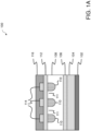
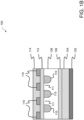
- FIGS. 1A and 1B are diagrams of exemplary buried grid double junction barrier Schottky diodes, according to some non-limiting embodiments or aspects of the presently disclosed subject matter.
- buried grid double junction barrier Schottky diode 100 may include at least one of metallization layer 102, substrate layer 104, buffer layer 106, drift layer 108, grid layer 110, grid spacing areas 111, regrown layer 112, first Schottky material layer 114, second Schottky material layer 116, and/or any combination thereof.
- Metallization layer 102 may include a layer of metal material and/or other conductive material.
- the metal and/or conductive material of metallization layer 102 may include a layer of aluminum (Al), silver (Ag), gold (Au), copper (Cu), titanium (Ti), nickel (Ni), an alloy of at least two metals, a compound including at least one metal, polysilicon, silicide, ohmic contact (e.g., silicidation), any combination thereof, and/or the like.
- ohmic contact e.g., silicidation
- a thin layer of nickel (Ni) followed by annealing (e.g., thermal annealing, laser annealing, and/or the like) to form a nickel silicide layer.
- annealing e.g., thermal annealing, laser annealing, and/or the like
- metal and/or conductive material may be deposited on the nickel silicide layer.
- Substrate layer 104 may include a layer of material on (e.g., above, in contact with, and/or the like) metallization layer 102.
- substrate layer 104 may include a layer of an n-type (e.g., lightly n-doped) semiconductor material, such as silicon carbide (SiC), silicon (Si), a compound including at least one semiconductor material, any combination thereof, and/or the like.
- substrate layer 104 may include a layer of highly conductive material (e.g., semiconductor material, metal material, any combination thereof, and/or the like).
- Buffer layer 106 may include a layer of material on (e.g., above, in contact with, and/or the like) substrate layer 104. Additionally or alternatively, buffer layer 106 may be above (and/or on and/or in contact with) metallization layer 102. In some non-limiting embodiments or aspects, buffer layer 106 may include a layer of an n + -type (e.g., highly n-doped) semiconductor material, such as silicon carbide (SiC), silicon (Si), a compound including at least one semiconductor material, any combination thereof, and/or the like. Additionally or alternatively, buffer layer 106 may include a layer of material with the same type of doping as substrate layer 104. In some non-limiting embodiments or aspects, buffer layer 106 may include an epitaxial buffer layer.
- n + -type semiconductor material such as silicon carbide (SiC), silicon (Si), a compound including at least one semiconductor material, any combination thereof, and/or the like.
- buffer layer 106 may include a layer
- Drift layer 108 may include a layer of material on (e.g., above, in contact with, and/or the like) buffer layer 106. Additionally or alternatively, drift layer 108 may be above (and/or on and/or in contact with) buffer layer 106, substrate layer 104, and/or metallization layer 102.
- buffer layer 106 may include a layer of an n-type (e.g., lightly n-doped) semiconductor material, such as silicon carbide (SiC), silicon (Si), a compound including at least one semiconductor material, any combination thereof, and/or the like. Additionally or alternatively, drift layer 108 may include a layer of material with the same type of doping as substrate layer 104 and/or buffer layer 106. In some non-limiting embodiments or aspects, drift layer 108 may include an epitaxial drift layer.
- Grid layer 110 may include a plurality of grid segments at least partially in (e.g., embedded in, in contact with, and/or the like) drift layer 108. As shown in FIGS. 1A and 1B , grid layer 110 includes three grid segments, but any suitable number of grid segments may be included. In some non-limiting embodiments or aspects, the grid segments of grid layer 110 may have a repeating structure in at least one direction. For example, the grid segments may have a repeating structure in a first direction, and the repeating structure may repeat with a regular distance in at least the first direction (e.g., grid segments shaped like bars of identical and/or substantially similar size are spaced apart by grid spacing areas 111 of identical and/or substantially similar size in the first direction).
- the grid segments may have a repeating structure in both a first direction and a second direction (e.g., instead of bars spaced linearly in one direction, the grid segments may be squares, circles, hemispheres, and/or any other suitable shape spaced apart by first grid spacing areas 111 of first identical and/or substantially similar size in the first direction and spaced apart by second grid spacing areas 111 of second identical and/or substantially similar size, wherein the first and second grid spacing areas 111 may be the same or different size).
- the plurality of grid segments may define at least one grid spacing area 111 between adjacent grid segments. As shown in FIGS.
- grid layer 110 may include a p-type (e.g., lightly p-doped) and/or p + -type (e.g., highly p-doped) semiconductor material, such as silicon carbide (SiC), silicon (Si), a compound including at least one semiconductor material, any combination thereof, and/or the like. Additionally or alternatively, grid layer 110 may include a layer of material with an opposite type of doping as substrate layer 104, buffer layer 106, and/or drift layer 108. In some non-limiting embodiments or aspects, grid layer 110 may include a layer of material with a higher doping level than drift layer 108.
- p-type e.g., lightly p-doped
- p + -type e.g., highly p-doped
- grid layer 110 may include a layer of material with an opposite type of doping as substrate layer 104, buffer layer 106, and/or drift layer 108.
- grid layer 110 may include a layer of material with a higher
- Regrown layer 112 may include a layer of material on (e.g., above, in contact with, and/or the like) drift layer 108 and/or grid layer 110.
- a top surface of grid layer 110 may be in a plane
- a top surface of drift layer 108 may be in the plane (e.g., the top surfaces of grid layer 110 and drift layer 108 may be in the same plane)
- regrown layer 112 may be on (e.g., above, in contact with, and/or the like) the top surfaces of the grid layer and the drift layer (e.g., on the plane).
- regrown layer 112 may include a layer of an n-type (e.g., lightly n-doped) semiconductor material, such as silicon carbide (SiC), silicon (Si), a compound including at least one semiconductor material, any combination thereof, and/or the like. Additionally or alternatively, regrown layer 112 may include a layer of material with the same type of doping as substrate layer 104, buffer layer 106, and/or drift layer 108. In some non-limiting embodiments or aspects, regrown layer 112 may include an epitaxial regrown layer.
- n-type semiconductor material such as silicon carbide (SiC), silicon (Si), a compound including at least one semiconductor material, any combination thereof, and/or the like.
- regrown layer 112 may include a layer of material with the same type of doping as substrate layer 104, buffer layer 106, and/or drift layer 108.
- regrown layer 112 may include an epitaxial regrown layer.
- First Schottky material layer 114 may include a layer of material at least partially overlapping (e.g., above and/or the like) the grid segments of grid layer 110.
- first Schottky material layer 114 may be at least partially on (e.g., above, in contact with, and/or the like) regrown layer 112.
- first Schottky material layer 114 may include a metal material and/or other conductive material.
- first Schottky material layer 114 may include a layer of titanium (Ti), titanium disulfide (TiS 2 ), Titanium nitride (TiN), Tungsten silicide (WSi 2 ), polysilicon, silicide, an alloy of at least two metals, a compound including at least one metal (e.g., a compound of at least one semiconductor material and at least one metal material), any combination thereof, and/or the like.
- first Schottky material layer 114 may be surface treated to adjust (e.g., reduce and/or the like) the Schottky barrier height thereof.
- surface treatment of first Schottky material layer 114 may include at least one of annealing, temperature treatment, ion sputtering, any combination thereof, and/or the like.
- Second Schottky material layer 116 may include a layer of material at least partially overlapping (e.g., above and/or the like) the grid spacing area(s) 111.
- second Schottky material layer 116 may be at least partially on (e.g., above, in contact with, and/or the like) regrown layer 112.
- second Schottky material layer 116 may include a metal material and/or other conductive material.
- second Schottky material layer 116 may include a layer of titanium (Ti), titanium disulfide (TiS 2 ), Titanium nitride (TiN), Tungsten silicide (WSi 2 ), polysilicon, silicide, an alloy of at least two metals, a compound including at least one metal (e.g., a compound of at least one semiconductor material and at least one metal material), any combination thereof, and/or the like.
- second Schottky material layer 116 may be surface treated to adjust (e.g., increase and/or the like) the Schottky barrier height thereof.
- surface treatment of second Schottky material layer 116 may include at least one of annealing, temperature treatment, ion sputtering, any combination thereof, and/or the like.
- second Schottky material layer 116 may have a different (e.g., higher, greater, and/or the like) Schottky barrier height than first Schottky material layer 114.
- second Schottky material layer 116 may include a different material than first Schottky material layer 114 (e.g., the different materials may have different Schottky barrier heights).
- second Schottky material layer 116 may be surface treated differently than first Schottky material layer 114 (e.g., even if first Schottky material layer 114 and second Schottky material layer 116 include the same material, first Schottky material layer 114 and second Schottky material layer 116 may have different Schottky barrier heights if first Schottky material layer 114 and second Schottky material layer 116 received different surface treatments).
- first Schottky material layer 114 may be surface treated to reduce the Schottky barrier height thereof
- second Schottky material layer 116 may be surface treated to increase the Schottky barrier height thereof.
- first Schottky material layer 114 and second Schottky material layer 116 may include different materials and may have received different surface treatments.
- second Schottky material layer 116 may have a higher Schottky barrier height than first Schottky material layer 114.
- first Schottky material layer 114 may include a lower Schottky barrier height material (LSBM)
- second Schottky material layer 116 may include a higher Schottky barrier height material (HSBM), as described herein.
- the LSBM may have a Schottky barrier height of 1 electron volt (eV) or less
- the HSBM may have a Schottky barrier height of 1.2 eV or more (e.g., 1.22 eV or more).
- first Schottky material layer 114 may be on (e.g., formed on top of and/or the like) second Schottky material layer 116, and second Schottky material layer 116 may be at least partially in first Schottky material layer 114 (e.g., as shown in FIG. 1B ).
- second Schottky material layer 116 may include a plurality of segments, and each respective segment of second Schottky material layer 116 may at least partially overlap a respective grid spacing area 111 of the grid spacing area(s) 111 defined between grid segments of grid layer 110 (e.g., as shown in FIG. 1B ).
- a width of each respective segment of second Schottky material layer 116 may be greater than or equal to the width of the respective grid spacing area 111. Alternatively, the width of each respective segment of second Schottky material layer 116 may be less than a width of the respective grid spacing area 111.
- second Schottky material layer 116 may be on (e.g., formed on top of and/or the like) first Schottky material layer 114, and first Schottky material layer 114 may be at least partially in second Schottky material layer 116 (e.g., as shown in FIG. 1A ).
- first Schottky material layer 114 may include a plurality of segments, and each respective segment of first Schottky material layer 114 may at least partially overlap a respective grid segment of grid layer 110 (e.g., as shown in FIG. 1A ).
- a width of each respective segment of first Schottky material layer 114 may be less than a width of the respective grid segment of grid layer 110. Alternatively, a width of each respective segment of first Schottky material layer 114 may be greater than or equal to a width of the respective grid segment of grid layer 110.
- first Schottky material layer 114 or second Schottky material layer 116 may include (e.g., may serve as) an anode. Additionally or alternatively, an additional layer of metal material (not pictured) may be deposited on first Schottky material layer 114 or second Schottky material layer 116 (e.g., whichever of these two layers is on top) to serve as an anode.
- buried grid double junction barrier Schottky diode 100 may include a cathode on an opposite side of drift layer 108 from the anode.
- metallization layer 102 may include (e.g., may serve as) a cathode.
- buried grid double junction barrier Schottky diode 100 may operate in a current conducting mode when a voltage (e.g., positive voltage) greater than a threshold voltage (V TH ) is applied from the anode to the cathode (e.g., voltage is applied in the forward direction). Additionally or alternatively, buried grid double junction barrier Schottky diode 100 may operate in a blocking mode (e.g., voltage blocking mode) when a voltage (e.g., positive voltage) is applied from the cathode to the anode (e.g., voltage is applied in the forward direction, negative voltage is applied from the anode to the cathode, and/or the like).
- a voltage e.g., positive voltage
- V TH threshold voltage
- buried grid double junction barrier Schottky diode 100 may operate in a blocking mode (e.g., voltage blocking mode) when a voltage (e.g., positive voltage) is applied from the cathode to the anode (e.
- FIGS. 1A and 1B The number and arrangement of layers and/or elements in FIGS. 1A and 1B are provided as an example. There may be additional layers and/or elements, fewer layers and/or elements, different layers and/or elements, and/or differently arranged layers and/or elements than those shown in FIGS. 1A and 1B . Furthermore, two or more layers and/or elements shown in FIGS. 1A and 1B may be implemented within a single layer and/or element, or a single layer and/or element shown in FIGS. 1A and 1B may be implemented as multiple layers and/or elements.
- a set of layers and/or set of elements of buried grid double junction barrier Schottky diode 100 may perform one or more functions described as being performed by another set of layers and/or another set of elements of buried grid double junction barrier Schottky diode 100.
- the doping of materials and/or layers described with respect to FIGS. 1A and 1B are provided as an example. There may be additional doping, less doping, and/or different doping than those described above. For example, all n-type and/or n + -type materials may be interchanged for p-type and/or p + -type, respectively, and vice versa (e.g., and the buried grid double junction barrier Schottky diode may still operate as described herein).
- FIG. 2 is a flowchart of an exemplary process 200 of making a buried grid double junction barrier Schottky diode, according to some non-limiting embodiments or aspects of the presently disclosed subject matter.
- the number and arrangement of steps shown in FIG. 2 are provided as an example. In some non-limiting embodiments or aspects, process 200 may include additional steps, fewer steps, different steps, or differently arranged steps than those shown in FIG. 2 .
- process 200 may include forming and/or providing a substrate layer.
- substrate layer 104 may be provided (e.g., may have been previously fabricated) as a layer of semiconductor material (e.g., n-type semiconductor material) upon which the other layers of buried grid double junction barrier Schottky diode 100 may be formed. Additionally or alternatively, substrate layer 104 may be formed.
- substrate layer 104 may be formed by forming a crystal of semiconductor material, slicing the crystal to form a wafer, and/or doping the crystal and/or the wafer to form substrate layer 104.
- process 200 may include forming a buffer layer.
- buffer layer 106 may be formed on one side (e.g., a top side, opposite side from metallization layer 102, and/or the like) of substrate layer 104.
- forming buffer layer 106 may include depositing a layer of semiconductor material (e.g., n + -type semiconductor material) on one side of substrate layer 104.
- depositing may include adhering buffer layer 106 to substrate layer 104, affixing buffer layer 106 to substrate layer 104, forming buffer layer 106 by epitaxy (e.g., epitaxial growth) on substrate layer 104, any combination thereof, and/or the like.
- buffer layer 106 may be doped (e.g., highly n-doped) after forming buffer layer 106. Additionally or alternatively, buffer layer 106 (and/or the material thereof) may be doped before and/or during forming (e.g., depositing) buffer layer 106.
- process 200 may include forming a drift layer.
- drift layer 108 may be formed on one side (e.g., a top side, opposite side from metallization layer 102, and/or the like) of buffer layer 106.
- forming drift layer 108 may include depositing a layer of semiconductor material (e.g., n-type semiconductor material) on one side of buffer layer 106.
- depositing may include adhering drift layer 108 to buffer layer 106, affixing drift layer 108 to buffer layer 106, forming drift layer 108 by epitaxy (e.g., epitaxial growth) on buffer layer 106, any combination thereof, and/or the like.
- drift layer 108 may be doped (e.g., lightly n-doped) after forming drift layer 108. Additionally or alternatively, drift layer 108 (and/or the material thereof) may be doped before and/or during forming (e.g., depositing) drift layer 108.
- process 200 may include forming a grid layer.
- grid layer 110 may be formed by patterning (e.g., by etching, lift-off, and/or the like) drift layer 108 to form a plurality of trenches and/or forming grid segments of grid layer 110 in the trenches.
- forming the grid segments of grid layer 110 may include depositing semiconductor material (e.g., p-type and/or p + -type semiconductor material) in the trenches of drift layer 108.
- depositing may include adhering the grid segments into the trenches, affixing the grid segments into the trenches, forming the grid segments by epitaxy (e.g., epitaxial growth) in the trenches, any combination thereof, and/or the like.
- forming grid layer 110 may include forming the grid segments of grid layer 110 by implantation.
- the grid segments of grid layer 110 may be doped (e.g., lightly p-doped, highly p-doped, and/or the like) after forming the grid segments of grid layer 110. Additionally or alternatively, the grid segments of grid layer 110 (and/or the material thereof) may be doped before and/or during forming (e.g., depositing) the grid segments of grid layer 110.
- process 200 may include forming a regrown layer.
- regrown layer 112 may be formed on drift layer 108 and/or grid layer 110.
- forming regrown layer 112 may include depositing a layer of semiconductor material (e.g., n-type semiconductor material) on top of drift layer 108 and/or grid layer 110.
- depositing may include adhering regrown layer 112 to drift layer 108 and/or grid layer 110, affixing regrown layer 112 to drift layer 108 and/or grid layer 110, forming regrown layer 112 by epitaxy (e.g., epitaxial growth) on drift layer 108 and/or grid layer 110, any combination thereof, and/or the like.
- epitaxy e.g., epitaxial growth
- regrown layer 112 may be doped (e.g., lightly n-doped) after forming regrown layer 112. Additionally or alternatively, regrown layer 112 (and/or the material thereof) may be doped before and/or during forming (e.g., depositing) regrown layer 112.
- process 200 may include forming a first Schottky material layer.
- first Schottky material layer 114 may be formed at least partially on (e.g., above, in contact with, and/or the like) regrown layer 112 and/or at least partially overlapping (e.g., above and/or the like) the grid segments of grid layer 110.
- forming first Schottky material layer 114 may include depositing a layer of metal material and/or other conductive material on regrown layer 112 (and/or second Schottky material layer 116).
- depositing may include sputtering first Schottky material layer 114 onto regrown layer 112 (and/or second Schottky material layer 116), depositing first Schottky material layer 114 onto regrown layer 112 (and/or second Schottky material layer 116) by evaporation, adhering first Schottky material layer 114 to regrown layer 112 (and/or second Schottky material layer 116), affixing first Schottky material layer 114 to regrown layer 112 (and/or second Schottky material layer 116), forming first Schottky material layer 114 by chemical vapor deposition (CVD) on regrown layer 112 (and/or second Schottky material layer 116), any combination thereof, and/or the like.
- CVD chemical vapor deposition
- first Schottky material layer 114 may be surface treated after forming first Schottky material layer 114. Additionally or alternatively, first Schottky material layer 114 (and/or the material thereof) may be surface treated before and/or during forming (e.g., depositing) first Schottky material layer 114.
- first Schottky material layer 114 may include forming an intermediate first Schottky material layer on regrown layer 112 (e.g., depositing a layer of metal material and/or other conductive material on regrown layer 112).
- the intermediate first Schottky material layer may be patterned (e.g., by etching, lift-off, and/or the like) to form first Schottky material layer 114 at least partially overlapping the grid segments of grid layer 110 (e.g., to form a plurality of segments of first Schottky material layer 114, each respective segment at least partially overlapping a respective grid segment of grid layer 110).
- second Schottky material layer 116 may be formed on first Schottky material layer 114 and/or regrown layer 112.
- process 200 may include forming a second Schottky material layer.
- second Schottky material layer 116 may be formed at least partially on (e.g., above, in contact with, and/or the like) regrown layer 112 and/or at least partially overlapping (e.g., above and/or the like) grid spacing area(s) 111.
- forming second Schottky material layer 116 may include depositing a layer of metal material and/or other conductive material on regrown layer 112 (and/or first Schottky material layer 114).
- depositing may include sputtering second Schottky material layer 116 onto regrown layer 112 (and/or first Schottky material layer 114), depositing second Schottky material layer 116 onto regrown layer 112 (and/or first Schottky material layer 114) by evaporation, adhering second Schottky material layer 116 to regrown layer 112 (and/or first Schottky material layer 114), affixing second Schottky material layer 116 to regrown layer 112 (and/or first Schottky material layer 114), forming second Schottky material layer 116 by CVD on regrown layer 112 (and/or first Schottky material layer 114), any combination thereof, and/or the like.
- second Schottky material layer 116 may be surface treated after forming second Schottky material layer 116. Additionally or alternatively, second Schottky material layer 116 (and/or the material thereof) may be surface treated before and/or during forming (e.g., depositing) second Schottky material layer 116.
- forming second Schottky material layer 116 may include forming an intermediate second Schottky material layer on regrown layer 112 (e.g., depositing a layer of metal material and/or other conductive material on regrown layer 112).
- the intermediate second Schottky material layer may be patterned (e.g., by etching, lift-off, and/or the like) to form second Schottky material layer 116 at least partially overlapping the grid spacing area(s) 111 (e.g., to form a plurality of segments of second Schottky material layer 116, each respective segment at least partially overlapping a respective grid spacing area 111).
- first Schottky material layer 114 may be formed on second Schottky material layer 116 and/or regrown layer 112.
- step 216 may come before step 214 (e.g., second Schottky material layer 116 may be formed initially, and first Schottky material layer 114 may be formed thereon). In some non-limiting embodiments or aspects, step 216 may come after step 214 (e.g., first Schottky material layer 114 may be formed initially, and second Schottky material layer 116 may be formed thereon).
- process 200 may include forming metallization layer.
- metallization layer 102 may be formed on one side (e.g., a bottom side; opposite side from buffer layer 106, drift layer 108, grid layer 110, regrown layer 112, first Schottky material layer 114, and/or second Schottky material layer 116; and/or the like) of substrate layer 104.
- substrate layer 104 may be formed and/or provided (e.g., may have been previously fabricated), as described herein, and forming metallization layer 102 may include depositing the layer of metal material and/or other conductive material on one side of substrate layer 104.
- depositing may include sputtering metallization layer 102 onto substrate layer 104, depositing metallization layer 102 onto substrate layer 104 by evaporation, adhering metallization layer 102 to substrate layer 104, affixing metallization layer 102 to substrate layer 104, forming metallization layer 102 by CVD on substrate layer 104, any combination thereof, and/or the like.
- ohmic contact e.g., silicidation
- a thin layer of nickel (Ni) followed by annealing (e.g., thermal annealing, laser annealing, and/or the like) to form a nickel silicide layer.
- annealing e.g., thermal annealing, laser annealing, and/or the like
- metal and/or conductive material may be deposited on the nickel silicide layer to form metallization layer 102.
- step 218 may come after step 204 (e.g., substrate layer 104 may be formed and/or provided, and metallization layer 102 may be formed thereon). In some non-limiting embodiments or aspects, step 218 may come after step 212, step 214, and/or step 216, as described herein.
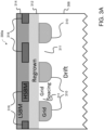
- FIG. 3A is a diagram of an exemplary implementation 300a of a buried grid double junction barrier Schottky diode, according to some non-limiting embodiments or aspects of the presently disclosed subject matter.
- implementation 300a may include at least one of drift layer 308, grid layer 310, grid spacing areas 311, regrown layer 312, LSBM layer 314, HSBM layer 316, and/or any combination thereof.
- implementation 300a may be the same as or similar to buried grid double junction barrier Schottky diode 100.
- drift layer 308 may be the same as or similar to drift layer 108.
- grid layer 310 may be the same as or similar to grid layer 110.
- grid spacing areas 311 may be the same as or similar to grid spacing areas 111.
- regrown layer 312 may be the same as or similar to regrown layer 112.
- LSBM layer 314 may be the same as or similar to first Schottky material layer 114.
- HSBM layer 316 may be the same as or similar to second Schottky material layer 116. The number and arrangement of layers and/or elements in FIG. 3A are provided as an example.
- implementation 300a may perform one or more functions described as being performed by another set of layers and/or another set of elements of implementation 300a.
- implementation 300a may include at least one additional layer below drift layer 308, such as a metallization layer, a substrate layer, a buffer layer, any combination thereof, and/or the like.
- LSBM layer 314 may be on (e.g., formed on top of and/or the like) HSBM layer 316, and HSBM layer 316 may be at least partially in LSBM layer 314, as described herein.
- HSBM layer 316 may include a plurality of segments, and each respective segment of HSBM layer 316 may at least partially overlap a respective grid spacing area 311 of the grid spacing area(s) 311 defined between grid segments of grid layer 310, as described herein.
- a width of each respective segment of HSBM layer 316 may be greater than or equal to the width of the respective grid spacing area 311.
- the width of each respective segment of HSBM layer 316 may be less than a width of the respective grid spacing area 311.
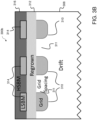
- FIG. 3B is a diagram of an exemplary implementation 300b of a buried grid double junction barrier Schottky diode, according to some non-limiting embodiments or aspects of the presently disclosed subject matter.
- implementation 300b may include at least one of drift layer 308, grid layer 310, grid spacing areas 311, regrown layer 312, LSBM layer 314, HSBM layer 316, and/or any combination thereof.
- implementation 300b may be the same as or similar to buried grid double junction barrier Schottky diode 100.
- drift layer 308 may be the same as or similar to drift layer 108.
- grid layer 310 may be the same as or similar to grid layer 110.
- grid spacing areas 311 may be the same as or similar to grid spacing areas 111.
- regrown layer 312 may be the same as or similar to regrown layer 112.
- LSBM layer 314 may be the same as or similar to first Schottky material layer 114.
- HSBM layer 316 may be the same as or similar to second Schottky material layer 116. The number and arrangement of layers and/or elements in FIG. 3B are provided as an example.
- implementation 300b may perform one or more functions described as being performed by another set of layers and/or another set of elements of implementation 300b.
- implementation 300b may include at least one additional layer below drift layer 308, such as a metallization layer, a substrate layer, a buffer layer, any combination thereof, and/or the like.
- HSBM layer 316 may have a higher Schottky barrier height than LSBM layer 314, as described herein.
- HSBM layer 316 may be on (e.g., formed on top of and/or the like) LSBM layer 314, and LSBM layer 314 may be at least partially in HSBM layer 316, as described herein.
- LSBM layer 314 may include a plurality of segments, and each respective segment of LSBM layer 314 may at least partially overlap a respective grid segment of grid layer 310, as described herein.
- a width of each respective segment of LSBM layer 314 may be less than a width of the respective grid segment of grid layer 310.
- a width of each respective segment of LSBM layer 314 may be greater than or equal to a width of the respective grid segment of grid layer 310.
- implementation 300a and/or implementation 300b may improve performance of the diode (e.g., compared to a diode having a single Schottky material layer) by lowering a threshold voltage (V TH ), improving (e.g., reducing) on-resistance, and maintaining and/or improving voltage blocking capabilities.
- V TH threshold voltage
- implementation 300a and/or implementation 300b may include semiconductor material layers of silicon carbide (SiC) and a buried grid (BG) junction barrier Schottky (JBS) structure with double Schottky contact materials.
- SiC silicon carbide
- BG buried grid
- JBS junction barrier Schottky
- an LSBM may be (at least partially) implemented above grid segments of grid layer 310 to reduce the threshold voltage (V TH ), and/or an HSBM may be (at least partially) implemented above grid spacing area(s) 311 to maintain and/or improve the blocking voltage (e.g., maintain and/or increase the blocking voltage) and leakage current (e.g., maintain and/or reduce the leakage current).
- V TH threshold voltage
- an HSBM may be (at least partially) implemented above grid spacing area(s) 311 to maintain and/or improve the blocking voltage (e.g., maintain and/or increase the blocking voltage) and leakage current (e.g., maintain and/or reduce the leakage current).
- one or more suitable Schottky materials may be used to form a barrier at the surface of the SiC layers (e.g., regrown layer 312, grid layer 310, and/or drift layer 308), and this may result in low forward voltage drop (V F ) and low leakage current.
- a thin regrown layer 312 between grid layer 310 and the Schottky material(s) may shield the Schottky contact areas from high electric fields in blocking mode, which may result in reduced leakage current.
- having two different Schottky material layers may reduce on-resistance and/or conduction loss.
- LSBM layer 314 may be (at least partially) implemented at the areas above grid segments of grid layer 310
- HSBM layer 316 may be (at least partially) implemented at the areas above the grid spacing areas 311.
- HSBM layer 316 may maintain and/or improve the leakage current (e.g., reduce the leakage current) and breakdown voltage (e.g., increase the breakdown voltage).
- LSBM layer 314 may start conducting earlier (e.g., at a lower voltage), resulting in a lower threshold voltage (V TH ), a lower forward voltage drop (V F ), and lower conduction loss (e.g., especially under low load conditions).
- V TH threshold voltage
- V F forward voltage drop
- V conduction loss e.g., especially under low load conditions
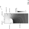
- FIG. 4 is a diagram of normalized electric field of an exemplary implementation 400 of a buried grid double junction barrier Schottky diode (e.g., in blocking mode), according to some non-limiting embodiments or aspects of the presently disclosed subject matter.
- implementation 400 may include drift layer 408, grid layer 410, grid spacing areas 411, regrown layer 412, LSBM layer 414, and HSBM layer 416.
- implementation 400 may be the same as or similar to buried grid double junction barrier Schottky diode 100, implementation 300a, and/or implementation 300b.
- drift layer 408 may be the same as or similar to drift layer 108 and/or drift layer 308.
- grid layer 410 may be the same as or similar to grid layer 110 and/or grid layer 310.
- grid spacing areas 411 may be the same as or similar to grid spacing areas 111 and/or grid spacing areas 311.
- regrown layer 412 may be the same as or similar to regrown layer 112 and/or regrown layer 312.
- LSBM layer 414 may be the same as or similar to first Schottky material layer 114 and/or LSBM layer 314.
- HSBM layer 416 may be the same as or similar to second Schottky material layer 116 and/or HSBM layer 316.
- the number and arrangement of layers and/or elements in FIG. 4 are provided as an example. There may be additional layers and/or elements, fewer layers and/or elements, different layers and/or elements, and/or differently arranged layers and/or elements than those shown in FIG. 4 . Furthermore, two or more layers and/or elements shown in FIG. 4 may be implemented within a single layer and/or element, or a single layer and/or element shown in FIG. 4 may be implemented as multiple layers and/or elements.
- implementation 400 may perform one or more functions described as being performed by another set of layers and/or another set of elements of implementation 400.
- implementation 400 may include at least one additional layer below drift layer 408, such as a metallization layer, a substrate layer, a buffer layer, any combination thereof, and/or the like.
- LSBM layer 414 above grid layer 410 may not affect the blocking capabilities of the diode (e.g., HSBM layer 316 allows the diode to maintain the blocking capabilities despite the inclusion of LSBM layer 314, even though a material with lower Schottky barrier height may otherwise be expected to reduce blocking capabilities).
- the electric field may be lowest in grid layer 410 and relatively low in the portion of regrown layer 412 above grid layer 410 and below LSBM layer 314.
- the electric field may be relatively higher in the portion of regrown layer 412 above grid spacing area 411 and below HSBM layer 416.
- the electric field may be even higher in grid spacing area 411 and the portion of drift layer 408 below grid spacing area 411.
- the electric field may be highest in the portion of drift layer 408 below grid layer 410.
- FIG. 5A shows graph 500a of reverse current density and voltage of an exemplary implementation of a buried grid double junction barrier Schottky diode, according to some non-limiting embodiments or aspects of the presently disclosed subject matter.
- graph 500a may include a vertical axis of current density (J) (e.g., in amperes per square centimeter (A/cm 2 )) and a horizontal axis of voltage (e.g., in volts (V)). Additionally, the vertical axis may include a logarithmic scale.
- first curve 501a may represent a buried grid junction barrier Schottky diode with a single Schottky material layer
- second curve 502a may represent a buried grid double junction barrier Schottky diode (e.g., with two Schottky material layers with different Schottky barrier heights), as described herein.
- second curve 502a may demonstrate the same or lower reverse current density (e.g., the same or reduced leakage current) compared to first curve 501a. Even at lower voltages, second curve 502a may demonstrate comparable reverse current density (e.g., maintain leakage current) compared to first curve 501a.
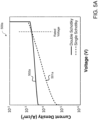
- FIG. 5B shows graph 500b of forward current density and voltage of an exemplary implementation of a buried grid double junction barrier Schottky diode, according to some non-limiting embodiments or aspects of the presently disclosed subject matter.
- graph 500b may include a vertical axis of current density (J) (e.g., in amperes per square centimeter (A/cm 2 )) and a horizontal axis of voltage (e.g., in volts (V)).
- J vertical axis of current density
- A/cm 2 amperes per square centimeter
- V horizontal axis of voltage
- first curve 501b may represent a buried grid junction barrier Schottky diode with a single Schottky material layer
- second curve 502b may represent a buried grid double junction barrier Schottky diode (e.g., with two Schottky material layers with different Schottky barrier heights), as described herein.
- Second curve 502b may demonstrate a lower threshold voltage (V TH ) compared to first curve 501b.
- second curve 502b may demonstrate a lower forward voltage drop (V F ) compared to first curve 501b.
- the buried grid double junction barrier Schottky diode described herein may reduce the area (and/or production cost) compared to a diode with a single Schottky material layer and still have the same forward voltage drop (V F ) at the rated current.
- FIG. 6 shows graph 600 of the ratio of the width of the first Schottky material layer to the width of the grid segments (W LSBM /W Grid ), forward voltage drop (V F ), and leakage current (I R ) of an exemplary implementation of a buried grid double junction barrier Schottky diode, according to some non-limiting embodiments or aspects of the presently disclosed subject matter. As shown in FIG.
- graph 600 may include a left vertical axis of forward voltage drop (V F ) (e.g., in volts (V)) at rated current, a right vertical axis of leakage current (I R ) (e.g., in amperes (A)) at rated voltage, and a horizontal axis of the ratio of the width of the first Schottky material layer (e.g., LSBM layer) to the width of the grid segments (W LSBM /W Grid ).
- V F forward voltage drop
- I R leakage current
- W LSBM /W Grid horizontal axis of the ratio of the width of the first Schottky material layer
- the left vertical axis may include a linear scale
- the right vertical axis may include a logarithmic scale.
- first curve 601 may represent a forward voltage drop (V F ) and second curve 602 may represent a leakage current (I R ) of a buried grid double junction barrier Schottky diode (e.g., with two Schottky material layers with different Schottky barrier heights (e.g., 1 eV as LSBM and 1.22 eV as HSBM)), as described herein.
- V F forward voltage drop
- I R leakage current
- increasing the width of the LSBM layer may reduce the forward voltage drop (V F ) but may increase the leakage current (I R ).
- Decreasing the width of the LSBM layer may increase the forward voltage drop (V F ) but may reduce the leakage current (I R ).
- the width of the LSBM layer (e.g., relative to the width of the grid segments) may be selected based on a target forward voltage drop (V F ), a target leakage current (I R ), any combination thereof, and/or the like.
- the Schottky barrier height of at least one of the LSBM layer and/or the HSBM layer may be adjusted (e.g., by selecting a different material and/or by applying a different surface treatment) based on a target forward voltage drop (V F ), a target leakage current (I R ), any combination thereof, and/or the like (e.g., and the width of the LSBM may be kept the same).
- the second Schottky material layer (e.g., HSBM layer) may cover all areas (e.g., of the regrown layer) not covered by the segments of the first Schottky material layer (e.g., LSBM layer).
Landscapes
- Electrodes Of Semiconductors (AREA)
Applications Claiming Priority (1)
| Application Number | Priority Date | Filing Date | Title |
|---|---|---|---|
| US18/303,617 US20240355938A1 (en) | 2023-04-20 | 2023-04-20 | Buried Grid Double Junction Barrier Schottky Diode and Method of Making |
Publications (1)
| Publication Number | Publication Date |
|---|---|
| EP4451338A1 true EP4451338A1 (de) | 2024-10-23 |
Family
ID=88290871
Family Applications (1)
| Application Number | Title | Priority Date | Filing Date |
|---|---|---|---|
| EP23201908.3A Pending EP4451338A1 (de) | 2023-04-20 | 2023-10-05 | Schottkydiode mit vergrabener doppelsperrschicht-gitter und verfahren zu deren herstellung |
Country Status (4)
| Country | Link |
|---|---|
| US (1) | US20240355938A1 (de) |
| EP (1) | EP4451338A1 (de) |
| KR (1) | KR102892530B1 (de) |
| CN (1) | CN118825084A (de) |
Citations (5)
| Publication number | Priority date | Publication date | Assignee | Title |
|---|---|---|---|---|
| JP2006352028A (ja) * | 2005-06-20 | 2006-12-28 | Sumitomo Electric Ind Ltd | 整流素子およびその製造方法 |
| US20080251793A1 (en) * | 2006-04-04 | 2008-10-16 | Semisouth Laboratories, Inc. | Junction barrier schottky rectifiers having epitaxially grown p+-n junctions and methods of making |
| CN104078515A (zh) * | 2014-04-21 | 2014-10-01 | 西安电子科技大学 | 基于外延工艺的沟槽式浮动结碳化硅sbd器件及其制造方法 |
| CN104157703A (zh) * | 2014-04-21 | 2014-11-19 | 西安电子科技大学 | 具有双金属的沟槽式浮动结碳化硅sbd器件 |
| CN112201697A (zh) * | 2020-09-24 | 2021-01-08 | 芜湖启源微电子科技合伙企业(有限合伙) | 肖特基二极管以及制备该肖特基二极管的方法 |
Family Cites Families (1)
| Publication number | Priority date | Publication date | Assignee | Title |
|---|---|---|---|---|
| ITUB20153251A1 (it) * | 2015-08-27 | 2017-02-27 | St Microelectronics Srl | Dispositivo a commutazione a semiconduttore ad ampia banda proibita con vasta area di giunzione schottky e relativo processo di fabbricazione |
-
2023
- 2023-04-20 US US18/303,617 patent/US20240355938A1/en active Pending
- 2023-10-05 EP EP23201908.3A patent/EP4451338A1/de active Pending
- 2023-10-30 CN CN202311425748.1A patent/CN118825084A/zh active Pending
- 2023-10-30 KR KR1020230147126A patent/KR102892530B1/ko active Active
Patent Citations (5)
| Publication number | Priority date | Publication date | Assignee | Title |
|---|---|---|---|---|
| JP2006352028A (ja) * | 2005-06-20 | 2006-12-28 | Sumitomo Electric Ind Ltd | 整流素子およびその製造方法 |
| US20080251793A1 (en) * | 2006-04-04 | 2008-10-16 | Semisouth Laboratories, Inc. | Junction barrier schottky rectifiers having epitaxially grown p+-n junctions and methods of making |
| CN104078515A (zh) * | 2014-04-21 | 2014-10-01 | 西安电子科技大学 | 基于外延工艺的沟槽式浮动结碳化硅sbd器件及其制造方法 |
| CN104157703A (zh) * | 2014-04-21 | 2014-11-19 | 西安电子科技大学 | 具有双金属的沟槽式浮动结碳化硅sbd器件 |
| CN112201697A (zh) * | 2020-09-24 | 2021-01-08 | 芜湖启源微电子科技合伙企业(有限合伙) | 肖特基二极管以及制备该肖特基二极管的方法 |
Also Published As
| Publication number | Publication date |
|---|---|
| CN118825084A (zh) | 2024-10-22 |
| KR20240155730A (ko) | 2024-10-29 |
| KR102892530B1 (ko) | 2025-11-28 |
| US20240355938A1 (en) | 2024-10-24 |
Similar Documents
| Publication | Publication Date | Title |
|---|---|---|
| US11342420B2 (en) | Heterojunction devices and methods for fabricating the same | |
| JP5011069B2 (ja) | 小さな寄生抵抗を有する低電圧ダイオードおよび製造方法 | |
| KR101774124B1 (ko) | 반도체 장치들 및 그것을 제조하는 방법 | |
| US7605441B2 (en) | Semiconductor device | |
| CN108039360B (zh) | 采用用于边缘终端元件的凹处的边缘终端结构 | |
| US9711599B2 (en) | Wide bandgap high-density semiconductor switching device and manufacturing process thereof | |
| US11949025B2 (en) | Wide band gap semiconductor electronic device having a junction-barrier Schottky diode | |
| US8956963B2 (en) | Schottky barrier diode and fabricating method thereof | |
| US12107173B2 (en) | Schottky rectifier with surge-current ruggedness | |
| US12349422B2 (en) | Semiconductor device | |
| US20220246771A1 (en) | Vertical conduction electronic device comprising a jbs diode and manufacturing process thereof | |
| US8592903B2 (en) | Bipolar semiconductor device and manufacturing method | |
| CN115206790B (zh) | 垂直结构肖特基二极管制作工艺及肖特基二极管 | |
| EP4451338A1 (de) | Schottkydiode mit vergrabener doppelsperrschicht-gitter und verfahren zu deren herstellung | |
| CN110534582B (zh) | 一种具有复合结构的快恢复二极管及其制造方法 | |
| CN112531007A (zh) | 具有梯度深度p型区域的结势垒肖特基二极管及制备方法 | |
| US8274128B2 (en) | Semiconductor device with buffer layer | |
| EP4531076A1 (de) | Herstellung eines schottky-kontakts in einem elektronischen bauelement wie einer jbs- oder mps-diode und elektronisches bauelement mit schottky-kontakt | |
| RU231051U1 (ru) | Диод Шоттки | |
| US12532488B2 (en) | Semiconductor device with selectively grown field oxide layer in edge termination region | |
| US20250275206A1 (en) | Plasma-free etched b-ga2o3-nio merged pin schottky diode with high-voltage stress reliability | |
| KR20250109561A (ko) | 질화물 반도체 소자 및 이의 제조방법 |
Legal Events
| Date | Code | Title | Description |
|---|---|---|---|
| PUAI | Public reference made under article 153(3) epc to a published international application that has entered the european phase |
Free format text: ORIGINAL CODE: 0009012 |
|
| STAA | Information on the status of an ep patent application or granted ep patent |
Free format text: STATUS: THE APPLICATION HAS BEEN PUBLISHED |
|
| AK | Designated contracting states |
Kind code of ref document: A1 Designated state(s): AL AT BE BG CH CY CZ DE DK EE ES FI FR GB GR HR HU IE IS IT LI LT LU LV MC ME MK MT NL NO PL PT RO RS SE SI SK SM TR |
|
| STAA | Information on the status of an ep patent application or granted ep patent |
Free format text: STATUS: REQUEST FOR EXAMINATION WAS MADE |
|
| 17P | Request for examination filed |
Effective date: 20250423 |