EP4531076A1 - Herstellung eines schottky-kontakts in einem elektronischen bauelement wie einer jbs- oder mps-diode und elektronisches bauelement mit schottky-kontakt - Google Patents
Herstellung eines schottky-kontakts in einem elektronischen bauelement wie einer jbs- oder mps-diode und elektronisches bauelement mit schottky-kontakt Download PDFInfo
- Publication number
- EP4531076A1 EP4531076A1 EP24199690.9A EP24199690A EP4531076A1 EP 4531076 A1 EP4531076 A1 EP 4531076A1 EP 24199690 A EP24199690 A EP 24199690A EP 4531076 A1 EP4531076 A1 EP 4531076A1
- Authority
- EP
- European Patent Office
- Prior art keywords
- metal layer
- laser beam
- forming
- semiconductor
- sic
- Prior art date
- Legal status (The legal status is an assumption and is not a legal conclusion. Google has not performed a legal analysis and makes no representation as to the accuracy of the status listed.)
- Pending
Links
Images


Classifications
-
- H—ELECTRICITY
- H10—SEMICONDUCTOR DEVICES; ELECTRIC SOLID-STATE DEVICES NOT OTHERWISE PROVIDED FOR
- H10D—INORGANIC ELECTRIC SEMICONDUCTOR DEVICES
- H10D62/00—Semiconductor bodies, or regions thereof, of devices having potential barriers
- H10D62/80—Semiconductor bodies, or regions thereof, of devices having potential barriers characterised by the materials
- H10D62/83—Semiconductor bodies, or regions thereof, of devices having potential barriers characterised by the materials being Group IV materials, e.g. B-doped Si or undoped Ge
- H10D62/832—Semiconductor bodies, or regions thereof, of devices having potential barriers characterised by the materials being Group IV materials, e.g. B-doped Si or undoped Ge being Group IV materials comprising two or more elements, e.g. SiGe
- H10D62/8325—Silicon carbide
-
- H—ELECTRICITY
- H10—SEMICONDUCTOR DEVICES; ELECTRIC SOLID-STATE DEVICES NOT OTHERWISE PROVIDED FOR
- H10D—INORGANIC ELECTRIC SEMICONDUCTOR DEVICES
- H10D64/00—Electrodes of devices having potential barriers
- H10D64/01—Manufacture or treatment
- H10D64/012—Manufacture or treatment of electrodes comprising a Schottky barrier to a semiconductor
- H10D64/0121—Manufacture or treatment of electrodes comprising a Schottky barrier to a semiconductor to Group IV semiconductors
- H10D64/0123—Manufacture or treatment of electrodes comprising a Schottky barrier to a semiconductor to Group IV semiconductors to silicon carbide
-
- H—ELECTRICITY
- H10—SEMICONDUCTOR DEVICES; ELECTRIC SOLID-STATE DEVICES NOT OTHERWISE PROVIDED FOR
- H10D—INORGANIC ELECTRIC SEMICONDUCTOR DEVICES
- H10D64/00—Electrodes of devices having potential barriers
- H10D64/60—Electrodes characterised by their materials
- H10D64/64—Electrodes comprising a Schottky barrier to a semiconductor
-
- H—ELECTRICITY
- H10—SEMICONDUCTOR DEVICES; ELECTRIC SOLID-STATE DEVICES NOT OTHERWISE PROVIDED FOR
- H10D—INORGANIC ELECTRIC SEMICONDUCTOR DEVICES
- H10D8/00—Diodes
- H10D8/01—Manufacture or treatment
- H10D8/051—Manufacture or treatment of Schottky diodes
-
- H—ELECTRICITY
- H10—SEMICONDUCTOR DEVICES; ELECTRIC SOLID-STATE DEVICES NOT OTHERWISE PROVIDED FOR
- H10D—INORGANIC ELECTRIC SEMICONDUCTOR DEVICES
- H10D8/00—Diodes
- H10D8/60—Schottky-barrier diodes
-
- H—ELECTRICITY
- H10—SEMICONDUCTOR DEVICES; ELECTRIC SOLID-STATE DEVICES NOT OTHERWISE PROVIDED FOR
- H10D—INORGANIC ELECTRIC SEMICONDUCTOR DEVICES
- H10D62/00—Semiconductor bodies, or regions thereof, of devices having potential barriers
- H10D62/10—Shapes, relative sizes or dispositions of the regions of the semiconductor bodies; Shapes of the semiconductor bodies
- H10D62/102—Constructional design considerations for preventing surface leakage or controlling electric field concentration
- H10D62/103—Constructional design considerations for preventing surface leakage or controlling electric field concentration for increasing or controlling the breakdown voltage of reverse-biased devices
- H10D62/105—Constructional design considerations for preventing surface leakage or controlling electric field concentration for increasing or controlling the breakdown voltage of reverse-biased devices by having particular doping profiles, shapes or arrangements of PN junctions; by having supplementary regions, e.g. junction termination extension [JTE]
- H10D62/106—Constructional design considerations for preventing surface leakage or controlling electric field concentration for increasing or controlling the breakdown voltage of reverse-biased devices by having particular doping profiles, shapes or arrangements of PN junctions; by having supplementary regions, e.g. junction termination extension [JTE] having supplementary regions doped oppositely to or in rectifying contact with regions of the semiconductor bodies, e.g. guard rings with PN or Schottky junctions
Definitions
- the present invention relates to a method of forming a metal-semiconductor Schottky contact, and an electronic device including the metal-semiconductor contact.
- JBS Junction Barrier Schottky
- MPS Merged-PN-Schottky
- 4H-SiC Due to the greater ease of manufacture compared to other polytypes, 4H-SiC is commonly used as a substrate.
- the band gap of 4H-SiC is greater (3.2 eV) than the corresponding band gap of 3C-SiC (2.3 eV) or Silicon (1.12 eV), making 4H-SiC less attractive to some electronic applications compared to 3C-SiC or compared to Silicon.
- the possibility of controlling the SBH value is an important aspect in order to reduce energy consumption and minimize conduction losses.
- Figure 1 shows, in lateral sectional view in a Cartesian (triaxial) reference system of axes X, Y, Z, a JBS (similarly MPS) device, identified with the reference number 1.
- JBS similarly MPS
- the JBS device 1 includes: a substrate 3, of N-type doped 4H-SiC, having a first dopant concentration (e.g., comprised between 1 ⁇ 10 19 and 1 ⁇ 10 22 atoms/cm 3 ), resistivity comprised for example between 2 m ⁇ cm and 40 m ⁇ cm, provided with a surface 3a opposite to a surface 3b, and a thickness comprised between 50 ⁇ m and 350 pm, more particularly between 160 ⁇ m and 200 pm, for example equal to 180 ⁇ m; a drift layer (epitaxially grown) 2, of N-type 4H-SiC, having a second dopant concentration lower than the first dopant concentration (for example comprised between 1 ⁇ 10 14 and 5 ⁇ 10 16 atoms/cm 3 ), which extends on the surface 3a of the substrate 3, and a thickness comprised between 5 and 15 pm; an ohmic contact region 6 (for example of Nickel Silicide), which extends on the surface 3b of the substrate 3; a cathode metall
- Schottky diodes 12 are formed at the interface between the drift layer 2 and the anode metallization 8.
- Schottky junctions semiconductor-metal are formed by portions of the drift layer 2 in direct electrical contact with respective portions of the anode metallization 8.
- the region of the JBS device 1 which includes the JB elements 9 and the Schottky diodes 12 is an active area 4 of the JBS device 1.
- the variables involved in the formation of the Schottky barrier are many, including the choice of the metal in contact with the surface 2a of the drift layer 2 and its evolution in the formation of the contact, with particular reference to the annealing step.
- Several studies have analyzed the electrical properties of various metallization patterns for Schottky contacts on 4H-SiC, with particular attention to the value of the Schottky barrier height and to the mechanisms of current transport through the metal/semiconductor interfaces.
- some technological questions are still open and deserve further investigation. For example, the possibility of controlling and lowering the Schottky barrier height is an important point to reduce the energy consumption of the device.
- US2017/170280A1 relates to a method and an apparatus for manufacturing a semiconductor element that is for forming an ohmic electrode on a silicon carbide (SiC) substrate, and the semiconductor element.
- US2022/406948A1 relates to a silicon carbide semiconductor device and a method of manufacturing a silicon carbide semiconductor device.
- US2022/384662A1 relates to a semiconductor merged-PN-Schottky (MPS) diode with reduced current-crowding effect and a manufacturing method thereof.
- MPS semiconductor merged-PN-Schottky
- US2021/143272A1 relates to manufacturing a semiconductor device by preventing precipitation of an oxide to prevent peeling of a resin layer.
- JP2014063948A relates to a method of manufacturing a silicon carbide semiconductor device, and more particularly, to a method of manufacturing a silicon carbide semiconductor device capable of suppressing the surface roughness of a silicon carbide substrate.
- the aim of the present invention is to provide a method of forming a metal-semiconductor contact, and an electronic device including the metal-semiconductor contact, such as to overcome the drawbacks of the prior art, and in particular a method which allows the SBH value to be reduced.
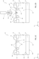
- FIG. 2A-2E illustrate the electronic device 20 in a triaxial system of axes X, Y, Z orthogonal to each other.
- the electronic device 20 (in particular a JBS device) is illustrated in an intermediate manufacturing step.
- the device 20 comprises a substrate 22 of semiconductor material, in particular silicon carbide 4H-SiC.
- semiconductor material in particular silicon carbide 4H-SiC.
- the present invention also finds application for other SiC polytypes such as for example the cubic polytype (3C-SiC), the hexagonal polytype (6H-SiC) and the rhombohedral polytype (15R-SiC).
- the substrate 22 is doped by doping species having a first electrical conductivity (in particular of N-type).
- the substrate 22 has a dopant concentration for example between 1 ⁇ 10 19 and 1 ⁇ 10 22 atoms/cm 3 (boundaries included) and a resistivity for example between 2 m ⁇ cm and 40 m ⁇ cm (boundaries included).
- the substrate 22 has an upper surface 22a opposite to a lower surface 22b along the direction Z, and a thickness (along the direction Z) comprised between 50 ⁇ m and 350 pm, more particularly between 160 ⁇ m and 200 pm, for example equal to 180 ⁇ m.
- the device 20 further comprises a drift layer (e.g., epitaxially grown) 24, here in particular of N-type 4H-SiC (similarly, it may be of 3C-SiC, 6H-SiC, 15H-SiC or other SiC polytypes).
- the drift layer 24 extends on the surface 22a of the substrate 22 and has an own upper surface 24a opposite, along the direction Z, to a lower surface 24b; the lower surface 24b of the drift layer is in contact with the upper surface 22a of the substrate 22.
- the drift layer 24 has a dopant concentration lower than the dopant concentration of the substrate 22 (for example between 1 ⁇ 10 14 and 5 ⁇ 10 16 atoms/cm 3 - boundaries included).
- the drift layer 24 has a thickness (along the direction Z) comprised between 3 and 30 ⁇ m.
- the substrate 22 and the drift layer 24 form, as a whole, a solid body of semiconductor material, in particular of SiC. Furthermore, it becomes apparent that one or more further semiconductor layers may be present between the substrate 22 and the drift layer 24; alternatively, the drift layer 24 may be absent: in this case, the steps described hereinbelow apply to the substrate 22.
- the device 20 further comprises a plurality of Junction-Barrier (JB) elements 26 in the drift layer 24, facing the upper surface 24a of the drift layer 24 and each including a respective implanted region 28' having a second conductivity (here of P-type) opposite to the first conductivity; an ohmic contact 28" is also present, in a per se known manner, at each implanted region 28'.
- JB Junction-Barrier
- the device 20 further comprises, optionally, an edge termination region, or protection ring, 30.
- the edge termination region 30 is in particular an implanted region having the second conductivity (P-type) and surrounds (completely or partially) the JB elements 26.
- a hard mask 35 is formed on the surface 24a of the drift layer 24, lateral to the JB elements 26 and surrounding the JB elements 26, and only partially superimposed on the edge termination region 30 where present.
- the hard mask 35 is for example of silicon oxide (SiO 2 ).
- an electrically conductive layer 32 of metal material in particular of Titanium or Titanium Nitride (TiN), or other metals and related nitrides (e.g., Mo, MoN), is formed on the upper surface 24a of the drift layer 24 and on the hard mask 35.
- the conductive layer 32 is formed for example by deposition of Titanium or Titanium Nitride.
- the electrically conductive layer 32 e.g., of TiN
- the percentage of N 2 in the gaseous mixture may vary between 0% (in this case a metal Ti layer is deposited, rather than a TiN layer) and 900.
- the percentage of N 2 in the gaseous mixture is about 75%.
- the conductive layer 32 has a thickness, along the direction Z, comprised between 10 and 100 nm (boundaries included).
- the conductive layer 32 has an exposed upper surface 32a, for a subsequent manufacturing step described with reference to Figure 2D .
- the conductive layer 32 extends in electrical contact with the JB elements 26 and with the drift layer 24, forming a Schottky contact (metal-semiconductor junction) with the drift layer 24 and, consequently, forming a respective Schottky diode 36.
- the region of the device 20 which includes the JB elements 26 and the Schottky contact i.e., the region contained within the protection ring 30, if present is an active area 38 of the device 20.
- the present invention provides an annealing step of the conductive layer 32 with the aim of adjusting the barrier height (SBH) of the Schottky contact formed at the step of Figure 2C .
- the annealing occurs using a LASER source 40 (e.g., excimer LASER) configured to emit a beam 42.
- LASER source 40 e.g., excimer LASER
- the configuration and operating parameters of the LASER source 40 are the following (boundaries of the ranges included):
- the area of the spot of the beam 42, at the level of the surface of the conductive layer 32, is, for example, comprised between 0.7 and 2.25 cm 2 .
- Such a spot area value may be obtained, for example, by the aid of suitable focusing lenses 43, in a per se known manner.
- the LASER beam is, in one embodiment, oriented along the direction Z; in other words, it reaches the upper surface 32a of the conductive layer 32 orthogonally to this surface 32a.
- the LASER beam may have a different orientation, for example it may form an angle with the direction Z (similarly, an angle with the portion of the surface 32a of the conductive layer 32 on which it impinges).
- the conductive layer 32 is heated uniformly (both orthogonally to the beam, along the directions X and Y, and longitudinally to the beam, along the direction Z).
- the annealing temperature reached at the level of the surface 32a of the conductive layer 32 is in particular comprised between 1800 and 3000 °C.
- a further conductive layer 46 (anode terminal) above, and in electrical contact with, the conductive layer 32.
- This further conductive layer 46 is for example of metal material, such as Al or Al alloys such as AlCu or AlSiCu, and is formed by Physical Vapor Deposition (PVD), in particular sputtering, at a temperature comprised between 200°C and 500°C, in particular 400°C.
- PVD Physical Vapor Deposition
- the conductive layer 46 has for example a thickness between 3 and 5 ⁇ m (boundaries included). The Applicant has verified that deposition temperature values outside the above-mentioned range result in poor stiction between the conductive layers 32 and 46.
- the manufacturing process described may also provide steps of forming a cathode electrical terminal at the lower surface 22b of the substrate 22, for example including an ohmic contact (e.g., nickel silicide) 50 on the lower surface 22b and a metallization on the ohmic contact 51 (illustrated in Figure 3 ).
- an ohmic contact e.g., nickel silicide
- the manufacturing method may further comprise a step of removing selective portions of the conductive layers 32 and 46, in order to remove such layers from regions of the device 20 wherein they do not have a function.
- the method may comprise a step of forming a passivation layer 52 (illustrated in Figure 3 ), to protect the device 20.
- the passivation layer extends above the conductive layer 46, except for portions of the conductive layer 46 used during subsequent steps of forming electrical contacts through bonding (e.g., wire bonding).
- the JBS device 20 includes: the substrate 22, of N-type 4H-SiC, having the first dopant concentration; the (epitaxial) drift layer 24, of N-type 4H-SiC, having the second dopant concentration; the conductive layer 32 on the surface 24a; the conductive layer 46 on the conductive layer 32; a cathode terminal 50 on the back of the substrate 22.
- the drift layer 24 comprises, as already described with reference to Figure 2A , the plurality of implanted regions 26, facing the upper surface 24a of the drift layer 24, at the interface with the conductive layer 32.
- Figure 3 also illustrates the ohmic contacts 28", extending at the (P-type) implanted regions 28' and forming, with the latter, respective JB elements 26.
- One or more Schottky diodes 36 extend at the interface between the conductive layer 32 and the drift layer 24, laterally to the implanted regions 26.
- one or more Schottky junctions are formed by portions of the conductive layer 32 in direct electrical contact with respective portions of the drift layer 24.
- the present invention is not limited to the manufacturing of SiC JBS or MPS devices, but extends to the generic formation of a metal-semiconductor contact (Schottky contact).
Landscapes
- Electrodes Of Semiconductors (AREA)
Applications Claiming Priority (1)
| Application Number | Priority Date | Filing Date | Title |
|---|---|---|---|
| IT102023000019941A IT202300019941A1 (it) | 2023-09-27 | 2023-09-27 | Formazione di un contatto schottky in un dispositivo elettronico, quale un diodo jbs o mps, e dispositivo elettronico con contatto schottky |
Publications (1)
| Publication Number | Publication Date |
|---|---|
| EP4531076A1 true EP4531076A1 (de) | 2025-04-02 |
Family
ID=88965269
Family Applications (1)
| Application Number | Title | Priority Date | Filing Date |
|---|---|---|---|
| EP24199690.9A Pending EP4531076A1 (de) | 2023-09-27 | 2024-09-11 | Herstellung eines schottky-kontakts in einem elektronischen bauelement wie einer jbs- oder mps-diode und elektronisches bauelement mit schottky-kontakt |
Country Status (5)
| Country | Link |
|---|---|
| US (1) | US20250107121A1 (de) |
| EP (1) | EP4531076A1 (de) |
| JP (1) | JP2025065010A (de) |
| CN (1) | CN119742229A (de) |
| IT (1) | IT202300019941A1 (de) |
Citations (5)
| Publication number | Priority date | Publication date | Assignee | Title |
|---|---|---|---|---|
| JP2014063948A (ja) | 2012-09-24 | 2014-04-10 | Sumitomo Electric Ind Ltd | 炭化珪素半導体装置の製造方法 |
| US20170170280A1 (en) | 2014-08-26 | 2017-06-15 | Sumitomo Heavy Industries, Ltd. | Method and apparatus for manufacturing semiconductor element, and semiconductor element |
| US20210143272A1 (en) | 2017-05-12 | 2021-05-13 | Mitsubishi Electric Corporation | Semiconductor device and power conversion apparatus |
| US20220384662A1 (en) | 2019-03-22 | 2022-12-01 | Stmicroelectronics S.R.L. | Semiconductor mps diode with reduced current-crowding effect and manufacturing method thereof |
| US20220406948A1 (en) | 2021-06-21 | 2022-12-22 | Fuji Electric Co., Ltd. | Silicon carbide semiconductor device and method of manufacturing silicon carbide semiconductor device |
-
2023
- 2023-09-27 IT IT102023000019941A patent/IT202300019941A1/it unknown
-
2024
- 2024-09-11 EP EP24199690.9A patent/EP4531076A1/de active Pending
- 2024-09-18 US US18/889,098 patent/US20250107121A1/en active Pending
- 2024-09-24 CN CN202411332219.1A patent/CN119742229A/zh active Pending
- 2024-09-25 JP JP2024166243A patent/JP2025065010A/ja active Pending
Patent Citations (5)
| Publication number | Priority date | Publication date | Assignee | Title |
|---|---|---|---|---|
| JP2014063948A (ja) | 2012-09-24 | 2014-04-10 | Sumitomo Electric Ind Ltd | 炭化珪素半導体装置の製造方法 |
| US20170170280A1 (en) | 2014-08-26 | 2017-06-15 | Sumitomo Heavy Industries, Ltd. | Method and apparatus for manufacturing semiconductor element, and semiconductor element |
| US20210143272A1 (en) | 2017-05-12 | 2021-05-13 | Mitsubishi Electric Corporation | Semiconductor device and power conversion apparatus |
| US20220384662A1 (en) | 2019-03-22 | 2022-12-01 | Stmicroelectronics S.R.L. | Semiconductor mps diode with reduced current-crowding effect and manufacturing method thereof |
| US20220406948A1 (en) | 2021-06-21 | 2022-12-22 | Fuji Electric Co., Ltd. | Silicon carbide semiconductor device and method of manufacturing silicon carbide semiconductor device |
Also Published As
| Publication number | Publication date |
|---|---|
| CN119742229A (zh) | 2025-04-01 |
| IT202300019941A1 (it) | 2025-03-27 |
| JP2025065010A (ja) | 2025-04-17 |
| US20250107121A1 (en) | 2025-03-27 |
Similar Documents
| Publication | Publication Date | Title |
|---|---|---|
| US11342420B2 (en) | Heterojunction devices and methods for fabricating the same | |
| TWI422029B (zh) | 具有抑制少數載體射入之碳化矽接合障礙蕭特基二極體 | |
| JP5390188B2 (ja) | ショットキーダイオードの性能を向上させる第2のショットキー接触金属層 | |
| JP4872158B2 (ja) | ショットキーダイオード、pn接合ダイオード、pin接合ダイオード、および製造方法 | |
| EP1633004B1 (de) | Schutzring for Halbleiteranordnungen | |
| US11670685B2 (en) | Doping activation and ohmic contact formation in a SiC electronic device, and SiC electronic device | |
| CN216719954U (zh) | 电子器件和用于制造电子器件的系统 | |
| CN113140639B (zh) | 一种碳化硅功率二极管及其制作方法 | |
| EP2184782A1 (de) | Schottky-barrieren-diode | |
| US10600921B2 (en) | Silicon carbide semiconductor device and method of manufacturing silicon carbide semiconductor device | |
| US8178949B2 (en) | Bipolar semiconductor device, method for producing the same, and method for controlling Zener voltage | |
| US20230299148A1 (en) | Forming an electronic device, such as a jbs or mps diode, based on 3c-sic, and 3c-sic electronic device | |
| US12414315B2 (en) | Silicon carbide Schottky barrier diode | |
| CN211828777U (zh) | 一种碳化硅功率二极管 | |
| CN115206790B (zh) | 垂直结构肖特基二极管制作工艺及肖特基二极管 | |
| JP6399161B2 (ja) | 半導体装置および半導体装置の製造方法 | |
| EP4531076A1 (de) | Herstellung eines schottky-kontakts in einem elektronischen bauelement wie einer jbs- oder mps-diode und elektronisches bauelement mit schottky-kontakt | |
| EP4156304A1 (de) | Siliziumkarbid-halbleiterbauelement und herstellungsverfahren | |
| EP4246554B1 (de) | Herstellung einer elektronischen vorrichtung, wie eine jbs oder mps diode, auf basis von 3c-sic, und 3c-sic elektronische vorrichtung | |
| US20250294822A1 (en) | Semiconductor device | |
| EP4451338A1 (de) | Schottkydiode mit vergrabener doppelsperrschicht-gitter und verfahren zu deren herstellung |
Legal Events
| Date | Code | Title | Description |
|---|---|---|---|
| PUAI | Public reference made under article 153(3) epc to a published international application that has entered the european phase |
Free format text: ORIGINAL CODE: 0009012 |
|
| STAA | Information on the status of an ep patent application or granted ep patent |
Free format text: STATUS: THE APPLICATION HAS BEEN PUBLISHED |
|
| AK | Designated contracting states |
Kind code of ref document: A1 Designated state(s): AL AT BE BG CH CY CZ DE DK EE ES FI FR GB GR HR HU IE IS IT LI LT LU LV MC ME MK MT NL NO PL PT RO RS SE SI SK SM TR |
|
| STAA | Information on the status of an ep patent application or granted ep patent |
Free format text: STATUS: REQUEST FOR EXAMINATION WAS MADE |
|
| 17P | Request for examination filed |
Effective date: 20250909 |