EP4425565A2 - Verfahren zur herstellung eines halbleiterbauelements und halbleiterbauelement - Google Patents
Verfahren zur herstellung eines halbleiterbauelements und halbleiterbauelement Download PDFInfo
- Publication number
- EP4425565A2 EP4425565A2 EP24160704.3A EP24160704A EP4425565A2 EP 4425565 A2 EP4425565 A2 EP 4425565A2 EP 24160704 A EP24160704 A EP 24160704A EP 4425565 A2 EP4425565 A2 EP 4425565A2
- Authority
- EP
- European Patent Office
- Prior art keywords
- gate
- semiconductor device
- layer
- channel region
- gate trench
- Prior art date
- Legal status (The legal status is an assumption and is not a legal conclusion. Google has not performed a legal analysis and makes no representation as to the accuracy of the status listed.)
- Pending
Links
Images




Classifications
-
- H—ELECTRICITY
- H10—SEMICONDUCTOR DEVICES; ELECTRIC SOLID-STATE DEVICES NOT OTHERWISE PROVIDED FOR
- H10D—INORGANIC ELECTRIC SEMICONDUCTOR DEVICES
- H10D62/00—Semiconductor bodies, or regions thereof, of devices having potential barriers
- H10D62/80—Semiconductor bodies, or regions thereof, of devices having potential barriers characterised by the materials
- H10D62/83—Semiconductor bodies, or regions thereof, of devices having potential barriers characterised by the materials being Group IV materials, e.g. B-doped Si or undoped Ge
- H10D62/832—Semiconductor bodies, or regions thereof, of devices having potential barriers characterised by the materials being Group IV materials, e.g. B-doped Si or undoped Ge being Group IV materials comprising two or more elements, e.g. SiGe
- H10D62/8325—Silicon carbide
-
- H—ELECTRICITY
- H10—SEMICONDUCTOR DEVICES; ELECTRIC SOLID-STATE DEVICES NOT OTHERWISE PROVIDED FOR
- H10D—INORGANIC ELECTRIC SEMICONDUCTOR DEVICES
- H10D30/00—Field-effect transistors [FET]
- H10D30/01—Manufacture or treatment
- H10D30/021—Manufacture or treatment of FETs having insulated gates [IGFET]
- H10D30/028—Manufacture or treatment of FETs having insulated gates [IGFET] of double-diffused metal oxide semiconductor [DMOS] FETs
- H10D30/0291—Manufacture or treatment of FETs having insulated gates [IGFET] of double-diffused metal oxide semiconductor [DMOS] FETs of vertical DMOS [VDMOS] FETs
- H10D30/0297—Manufacture or treatment of FETs having insulated gates [IGFET] of double-diffused metal oxide semiconductor [DMOS] FETs of vertical DMOS [VDMOS] FETs using recessing of the gate electrodes, e.g. to form trench gate electrodes
-
- H—ELECTRICITY
- H10—SEMICONDUCTOR DEVICES; ELECTRIC SOLID-STATE DEVICES NOT OTHERWISE PROVIDED FOR
- H10D—INORGANIC ELECTRIC SEMICONDUCTOR DEVICES
- H10D30/00—Field-effect transistors [FET]
- H10D30/60—Insulated-gate field-effect transistors [IGFET]
- H10D30/64—Double-diffused metal-oxide semiconductor [DMOS] FETs
- H10D30/66—Vertical DMOS [VDMOS] FETs
- H10D30/668—Vertical DMOS [VDMOS] FETs having trench gate electrodes, e.g. UMOS transistors
-
- H—ELECTRICITY
- H10—SEMICONDUCTOR DEVICES; ELECTRIC SOLID-STATE DEVICES NOT OTHERWISE PROVIDED FOR
- H10D—INORGANIC ELECTRIC SEMICONDUCTOR DEVICES
- H10D62/00—Semiconductor bodies, or regions thereof, of devices having potential barriers
- H10D62/10—Shapes, relative sizes or dispositions of the regions of the semiconductor bodies; Shapes of the semiconductor bodies
- H10D62/102—Constructional design considerations for preventing surface leakage or controlling electric field concentration
- H10D62/103—Constructional design considerations for preventing surface leakage or controlling electric field concentration for increasing or controlling the breakdown voltage of reverse-biased devices
- H10D62/105—Constructional design considerations for preventing surface leakage or controlling electric field concentration for increasing or controlling the breakdown voltage of reverse-biased devices by having particular doping profiles, shapes or arrangements of PN junctions; by having supplementary regions, e.g. junction termination extension [JTE]
-
- H—ELECTRICITY
- H10—SEMICONDUCTOR DEVICES; ELECTRIC SOLID-STATE DEVICES NOT OTHERWISE PROVIDED FOR
- H10D—INORGANIC ELECTRIC SEMICONDUCTOR DEVICES
- H10D62/00—Semiconductor bodies, or regions thereof, of devices having potential barriers
- H10D62/10—Shapes, relative sizes or dispositions of the regions of the semiconductor bodies; Shapes of the semiconductor bodies
- H10D62/102—Constructional design considerations for preventing surface leakage or controlling electric field concentration
- H10D62/103—Constructional design considerations for preventing surface leakage or controlling electric field concentration for increasing or controlling the breakdown voltage of reverse-biased devices
- H10D62/105—Constructional design considerations for preventing surface leakage or controlling electric field concentration for increasing or controlling the breakdown voltage of reverse-biased devices by having particular doping profiles, shapes or arrangements of PN junctions; by having supplementary regions, e.g. junction termination extension [JTE]
- H10D62/106—Constructional design considerations for preventing surface leakage or controlling electric field concentration for increasing or controlling the breakdown voltage of reverse-biased devices by having particular doping profiles, shapes or arrangements of PN junctions; by having supplementary regions, e.g. junction termination extension [JTE] having supplementary regions doped oppositely to or in rectifying contact with regions of the semiconductor bodies, e.g. guard rings with PN or Schottky junctions
- H10D62/107—Buried supplementary regions, e.g. buried guard rings
-
- H—ELECTRICITY
- H10—SEMICONDUCTOR DEVICES; ELECTRIC SOLID-STATE DEVICES NOT OTHERWISE PROVIDED FOR
- H10D—INORGANIC ELECTRIC SEMICONDUCTOR DEVICES
- H10D62/00—Semiconductor bodies, or regions thereof, of devices having potential barriers
- H10D62/10—Shapes, relative sizes or dispositions of the regions of the semiconductor bodies; Shapes of the semiconductor bodies
- H10D62/124—Shapes, relative sizes or dispositions of the regions of semiconductor bodies or of junctions between the regions
- H10D62/126—Top-view geometrical layouts of the regions or the junctions
- H10D62/127—Top-view geometrical layouts of the regions or the junctions of cellular field-effect devices, e.g. multicellular DMOS transistors or IGBTs
-
- H—ELECTRICITY
- H10—SEMICONDUCTOR DEVICES; ELECTRIC SOLID-STATE DEVICES NOT OTHERWISE PROVIDED FOR
- H10D—INORGANIC ELECTRIC SEMICONDUCTOR DEVICES
- H10D64/00—Electrodes of devices having potential barriers
- H10D64/01—Manufacture or treatment
- H10D64/013—Manufacture or treatment of electrodes having a conductor capacitively coupled to a semiconductor by an insulator
- H10D64/01366—Manufacture or treatment of electrodes having a conductor capacitively coupled to a semiconductor by an insulator the semiconductor being silicon carbide
-
- H—ELECTRICITY
- H10—SEMICONDUCTOR DEVICES; ELECTRIC SOLID-STATE DEVICES NOT OTHERWISE PROVIDED FOR
- H10D—INORGANIC ELECTRIC SEMICONDUCTOR DEVICES
- H10D64/00—Electrodes of devices having potential barriers
- H10D64/20—Electrodes characterised by their shapes, relative sizes or dispositions
- H10D64/27—Electrodes not carrying the current to be rectified, amplified, oscillated or switched, e.g. gates
- H10D64/311—Gate electrodes for field-effect devices
- H10D64/411—Gate electrodes for field-effect devices for FETs
- H10D64/511—Gate electrodes for field-effect devices for FETs for IGFETs
- H10D64/514—Gate electrodes for field-effect devices for FETs for IGFETs characterised by the insulating layers
-
- H—ELECTRICITY
- H10—SEMICONDUCTOR DEVICES; ELECTRIC SOLID-STATE DEVICES NOT OTHERWISE PROVIDED FOR
- H10D—INORGANIC ELECTRIC SEMICONDUCTOR DEVICES
- H10D64/00—Electrodes of devices having potential barriers
- H10D64/20—Electrodes characterised by their shapes, relative sizes or dispositions
- H10D64/27—Electrodes not carrying the current to be rectified, amplified, oscillated or switched, e.g. gates
- H10D64/311—Gate electrodes for field-effect devices
- H10D64/411—Gate electrodes for field-effect devices for FETs
- H10D64/511—Gate electrodes for field-effect devices for FETs for IGFETs
- H10D64/514—Gate electrodes for field-effect devices for FETs for IGFETs characterised by the insulating layers
- H10D64/516—Gate electrodes for field-effect devices for FETs for IGFETs characterised by the insulating layers the thicknesses being non-uniform
-
- H—ELECTRICITY
- H10—SEMICONDUCTOR DEVICES; ELECTRIC SOLID-STATE DEVICES NOT OTHERWISE PROVIDED FOR
- H10P—GENERIC PROCESSES OR APPARATUS FOR THE MANUFACTURE OR TREATMENT OF DEVICES COVERED BY CLASS H10
- H10P30/00—Ion implantation into wafers, substrates or parts of devices
- H10P30/20—Ion implantation into wafers, substrates or parts of devices into semiconductor materials, e.g. for doping
- H10P30/22—Ion implantation into wafers, substrates or parts of devices into semiconductor materials, e.g. for doping using masks
Definitions
- the present disclosure relates to a method of manufacturing semiconductor device and semiconductor device thereof.
- Ron on-resistance
- An aspect of the disclosure provides a method of manufacturing a semiconductor device.
- the method includes providing a substrate, wherein the substrate is SiC base, and the substrate sequentially includes, from bottom to top, an N-type heavy doping base layer, an N-type light doping layer, a P-well region, and a N-type heavy doping layer.
- the substrate is etched using a patterned mask to form at least one gate trench and a channel region defined by the at least one gate trench, wherein the channel region is covered by the patterned mask.
- An ion implantation process is performed to the at least one gate trench to form a shielding implant layer at a bottom surface of the at least one gate trench.
- An oxidation process is performed to the at least one gate trench to form a gate oxide layer, wherein an oxidation rate at the bottom surface of the at least one gate trench is faster than an oxidation rate at a sidewall of the at least one gate trench.
- At least one gate electrode is formed in the at least one gate trench.
- ions utilized in the ion implantation process includes P, As, or Ar.
- the method further includes removing the patterned mask after the performing the ion implantation process to the at least one gate trench.
- the method further includes performing an annealing process after removing the patterned mask, in which the annealing process is performed in an inert gas environment at the temperature of about 1700 Celsius degrees for about 30 minutes.
- etching the substrate to form at least one gate trench is performed such that the sidewall of the at least one gate trench has an inclined angle, in which the inclined angle is in a range from 75 degrees to 105 degrees.
- performing the ion implantation process to the at least one gate trench is performed vertical to the bottom surface of the at least one gate trench.
- performing the ion implantation process to the at least one gate trench is performed inclined towards the channel region.
- the semiconductor device includes a channel region disposed on an N-type heavy doping base layer, the channel region sequentially includes, from the N-type heavy doping base layer, an N-type light doping layer, a P-well region, and a N-type heavy doping layer, wherein the channel region and the N-type heavy doping base layer are SiC base.
- the semiconductor device includes at least one gate electrode disposed on at least one sidewall of the channel region, wherein top surfaces of the gate electrode are coplanar with a top surface of the channel region, and at least one gate oxide layer covering sidewalls and bottom surfaces of the gate electrode, respectively, wherein a thickness of the gate oxide layer at the bottom surface of the gate electrode is not less than a thickness of the gate oxide layer at the sidewall of the gate electrode.
- a number of the at least one gate electrode and the at least one gate oxide layer is two, and the gate electrodes are disposed at opposite sides of the channel region.
- the semiconductor device includes two shielding implant layers disposed below the gate oxide layers, respectively, wherein a bottom width of each of the gate electrodes is equal to or less than a width of each of the shielding implant layers.
- a width of each of the gate oxide layers is equal to the width of each of the shielding implant layers.
- the width of each of the shielding implant layers is greater than a width of each of the gate oxide layers, and each of the shielding implant layers single side extends into the channel region below each of the gate oxide layers.
- a number of the at least one gate electrode and the at least one gate oxide layer is one, and the gate electrode continuously surrounds the channel region.
- the semiconductor device further includes a shielding implant layer disposed below the gate oxide layer, wherein a bottom width of the gate electrode is equal to or less than a width of the shielding implant layer.
- the gate oxide layer includes a first portion at the sidewall of the gate electrode and a second portion at the bottom surface of the gate electrode, a thickness of the first portion is in a range from 30 nm to 200 nm, and a thickness of the second portion is in a range from 30 nm to 400 nm.
- the disclosure provides a method of manufacturing semiconductor device and semiconductor device thereof.
- the shielding implant layer is formed at the bottom of the gate trench by using the self-aligned ion implantation process.
- the shielding implant layer disposed below the gate electrode and the gate oxide layer can reduce the bottom electric field of the gate oxide layer, so the gate oxide layer would be much reliable due to the electric field applied on the gate oxide layer would be lower than the breakdown voltage of the gate oxide layer.
- the oxidation rates at the sidewall and the bottom of the gate trench are not the same because of the self-aligned ion implantation process, so that the formed gate oxide layer has the bottom thickness not less than the sidewall thickness to further reduce the bottom electric field of the gate oxide layer of the semiconductor device having trench type gate.
- relative terms such as “lower” or “bottom” and “upper” or “top”, may be used herein to describe one element's relationship to another element as illustrated in the Figures. It will be understood that relative terms are intended to encompass different orientations of the device in addition to the orientation depicted in the Figures. For example, if the device in one of the figures is turned over, elements described as being on the “lower” side of other elements would then be oriented on “upper” sides of the other elements. The exemplary term “lower”, can therefore, encompasses both an orientation of “lower” and “upper”, depending of the particular orientation of the figure.
- the trench type transistor is the trend of the development of the high power transistors because of the lower on-resistance (Ron), comparing to the planar type transistor.
- Ron on-resistance
- the performance of the conventional trench type transistor is limited by only one side conductive or the large pitches between the trenches.
- another problem of the trench type transistor is that the oxide layer at the trench bottom leads to large electric field so that the reliability of the device performance is reduced.
- Typical solutions include implanting extra P-type dopants to control the electric field or thickening the oxide layer at the trench bottom.
- implanting extra P-type dopants would leads to additional JFET effect which influences the on-resistance, and thickening the oxide layer at the trench bottom needs additional process steps which increases the complication of the manufacturing processes.
- an aspect of the disclosure is to provide a trench type transistor that has multiple gates or continuous gate, to enlarge the on-current by reducing the on-resistance, and a self-aligned P-type dopant implantation is performed following the formation of the trench to reduce the electric field of the gate oxide layer at the trench bottom.
- the implant region such as at the bottom of the trench has a faster oxidation rate, thus the thickness of the gate oxide layer is thicker than other portions to reduce the electric field of the gate oxide layer at the trench bottom, without adding additional process.
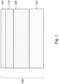
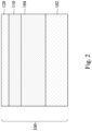
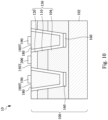
- Fig. 1 to Fig. 3 and Fig. 5 to Fig. 10 are cross-sectional views of different fabricating steps of forming a semiconductor device according to some embodiments of the disclosure.
- an ion implantation process is performed to a substrate 100, such that a P-well region 110 is defined in the substrate 100.
- the substrate 100 can be a semiconductor substrate such as a SiC substrate.
- the SiC is a semiconductor material that has wide energy band gap, so the SiC has greater breakdown voltage and lower current leakage. Additionally, the thermal conductivity of SiC material is better than the Si material, so that the SiC is suitable to be utilized in devices which are operated at high temperature environment such as transistors utilized in vehicles.
- the substrate 100 includes an N-type heavy doping base layer 102 and an N-type light doping layer 104 epitaxially grown on the N-type heavy doping base layer 102.
- the doping concentration of the N-type heavy doping base layer 102 is greater than 5 ⁇ 10 18 /cm 3
- the doping concentration of the N-type light doping layer 104 is between 5 ⁇ 10 16 /cm 3 and 5 ⁇ 10 17 /cm 3 , depending on the manufacturing process and the design of the device.
- the N-type heavy doping base layer 102 and N-type light doping layer 104 can be formed by ion implantation processes.
- the implant depth of the P-well region 110 is lower than the top surface of the substrate 100, such that a portion of the N-type light doping layer 104 is remained above the P-well region 110 after the P-type dopant implantation is performed.
- the doping concentration of the P-well region 110 is between 5 ⁇ 10 15 /cm 3 and 1 ⁇ 10 18 /cm 3 .
- an N-type implantation process is performed to the substrate 100 so that the portion of the N-type light doping layer 104 (as shown in Fig. 1 ) above the P-well region 110 becomes a N-type heavy doping layer 120.
- the doping concentration of the N-type heavy doping layer 120 is greater than 5 ⁇ 10 18 cm 3 .
- the thickness of the P-well region 110 is in a range from 0.3 ⁇ m to 1.3 ⁇ m, and the thickness of the N-type heavy doping layer 120 is in a range from 0.5 ⁇ m to 1.3 ⁇ m.
- a patterned mask 130 is formed on the substrate 100.
- the patterned mask 130 covers the regions that are pre-defined as channel regions, and the regions that are pre-defined as gates are exposed from the patterned mask 130.
- an etching process is performed, including the etching process using dry etching or wet etching to remove the portions of substrate 100 that are not covered by the patterned mask 130.
- the etching process stops at the N-type light doping layer 104, and portions of the P-well region 110 and the N-type heavy doping layer 120 uncovered by the patterned mask 130 are removed thereby defining one or more gate trenches 140 in the substrate 100. Portions of the P-well region 110 and the N-type heavy doping layer 120 protected by the patterned mask 130 and a portion of N-type light doping layer 104 serve as channel region 150.
- the number of the gate trenches 140 is two, and the gate trenches 140 are linear trenches that are parallelly arranged, and the gate trench 140 are arranged at opposite sides of the linear channel region 150. In some embodiments, as shown in Fig.5 , the number of gate trench 140 is one, and the gate trench 140 is a continuous ring or polygon trench that surround the channel region 150.
- the sidewall 142 of the gate trench 140 can be a vertical sidewall or an inclined sidewall.
- the angle ⁇ between the sidewall 142 and bottom surface 144 of the gate trench 140 is in a range between 75 degrees to 105 degrees.
- the bottom width W1 of the gate trench 140 is less than the top width of the gate trench 140 to reduce the punch through issue. In some other embodiments, the bottom width W1 of the gate trench 140 is greater than the top width of the gate trench 140 to enlarge the current path.
- an ion implantation process is performed to the gate trench 140 to form a shielding implant layer 160 at the bottom surface 144 of the gate trench 140.
- an angle of performing the ion implantation process is vertical to the bottom surface 144 of the gate trench 140. Because the top surfaces of the channel region 150 are still protected by the patterned mask 130, so that the ions distributed to the sidewalls of the channel region 150 is limited. Further, an additional process can be performed on the sidewalls of the channel region 150, to prevent the sidewalls of the channel region 150 from being affected by the ion implantation process.
- the ion species selected in the ion implantation process are able to change the characteristic of the SiC base substrate 100.
- the ions used in the ion implantation process can be P or other ion having larger atomic amount such as As, or noble gas such as Ar.
- the bottom surface 144 of the gate trench 140 is bombarded by the selected ions and has a faster oxidation rate than the sidewall 142 of the gate trench 140, under the same oxidation conditions.
- the process of defining the gate trench 140 and the process of forming the shielding implant layer 160 use the same patterned mask 130, so the implantation process can be referred as a self-aligned implantation process, and the fabricating complication can be reduced.
- an annealing process is performed in an inert gas environment to active the doped ions in the channel region 150 and the shielding implant layer 160.
- the annealing process is performed at the temperature of about 1700 Celsius degrees for about 30 minutes.
- the ions doped in the shielding implant layer 160 may diffuse and extend into the channel region 150 after the annealing process is performed.
- an oxidation process is performed.
- the oxidation process includes performing an annealing process to the semiconductor structure that has been ion implanted and thermal annealed in an oxygen-containing environment. Because the doped ion concentration and/or the silicon lattice are different at the bottom surface 144 of the gate trench 140 and the sidewall 142 of the gate trench 140, the oxidation rates of the bottom surface 144 of the gate trench 140 and the sidewall 142 of the gate trench 140 are different even under the same oxidation conditions.
- the oxidation rate at the bottom surface 144 of the gate trench 140 is significantly faster than the oxidation rate at the sidewall 142 of the gate trench 140, such that a gate oxide layer 170 formed by the single oxidation process has different thicknesses at the sidewall 142 of the gate trench 140 and the bottom surface 144 of the gate trench 140.
- the gate oxide layer 170 has a first portion 172 formed on the sidewall 142 of the gate trench 140 and a second portion 174 formed on the bottom surface 144 of the gate trench 140, in which the thickness T1 of the first portion 172 is less than the thickness T2 of the second portion 174.
- the first portion 172 of the gate oxide layer 170 on the sidewall of the channel region 150 has the thickness T1 less than the thickness T2 of the second portion 174 of the gate oxide layer 170 on the shielding implant layer 160.
- the gate oxide layer 170 having a thicker thickness at the bottom is benefit to reduce the electric field of the gate oxide layer 170 at the bottom of the ate trench 140.
- the thickness T2 of the second portion 174 of the gate oxide layer 170 can be similar to the thickness T1 of the first portion 172. Namely, the thickness T2 of the second portion 174 of the gate oxide layer 170 is not less than the thickness T1 of the first portion 172.
- the thickness T1 of the first portion 172 of the gate oxide layer 170 is from 30 nm to 200 nm. If the thickness T1 of the first portion 172 is too thin such as thinner than 30 nm, the problem of product reliability is raised. If the thickness T1 of the first portion 172 is too thick such as thinner than 200 nm, the driving current of the device is reduced.
- the thickness T2 of the second portion 174 of the gate oxide layer 170 is from 30 nm to 400 nm. If the thickness T2 of the second portion 174 is too thin such as thinner than 30 nm, the problem of product reliability is raised. If the thickness T2 of the second portion 174 is too thick such as thinner than 400 nm, the driving current of the device is reduced.
- a gate electrode material is filled in the gate trench 140 (as shown in Fig. 8 ), and a planarization process is performed to form the gate electrode 180 in the gate trench 140.
- the top surface 180T of the gate electrode 180 is coplanar with the top surface 150T of the channel region 150.
- the gate electrode 180 may include a barrier layer, a work function adjusting layer, an adhesive layer, and a body metal layer (such as W, Cu, Co, Ru, etc.).
- the trench type gate electrode 180 can further reduce the on-resistance of the semiconductor device, comparing to the planar type transistor.
- the bottom width W3 of the gate electrode 180 can be greater than, equal to, or smaller than the width W4 of the shielding implant layer 160.
- the shielding implant layer 160 disposed below the gate electrode 180 and the gate oxide layer 170 can reduce the bottom electric field of the gate oxide layer 170, so the gate oxide layer 170 would be much reliable due to the electric field applied on the gate oxide layer 170 would be lower than the breakdown voltage of the gate oxide layer 170.
- the gate oxide layer 170 covers the bottom and the sidewall of the gate electrode 180, and the second portion 174 of the gate oxide layer 170 at the bottom of gate electrode 180 has the thickness T2 not less than the thickness T1 of the first portion 172 of the gate oxide layer 170 at the sidewall of the gate electrode 180.
- a plurality of gate contacts 190 are formed on the top surface 180T of the gate electrode 180, and a plurality of source contact 200 are formed on the top surface 150T of the channel region 150, to continue the following backend processes.
- the N-type heavy doping base layer 102 can be served as the drain or common drain (if multiple transistors).
- the semiconductor device 10 includes the transistor is provided. By selectively applying voltage to the gate electrode 180, the channel region 150 is selectively conducted.
- the current conducting direction of the trench type gate electrode 180 is substantially same as the current conducting direction of the channel region 150.
- Fig. 11 is a cross-sectional view of the semiconductor device according to some other embodiments of the disclosure.
- the implant angle of the process of performing the ion implantation process to the gate trench 140 to formed the shielding implant layer 160 at the bottom of the gate trench 140 as shown in Fig. 6 is not 90 degrees, and the implant angle is inclined towards the channel region 150, the formed shielding implant layer 160 would single side extend into the region between the gate trench 140 and exist below the gate electrode 180 and at the bottom corner of the channel region 150.
- This shielding implant layer 160 formed by inclined implantation can further protect the gate oxide layer 170 at the bottom corner of the gate electrode 180 to further improve the reliability of the semiconductor device 10.
- the corona discharge is easily induced at the bottom corner of the gate electrode 180 so the bottom corner of the gate electrode 180 has higher electric field than other positions.
- the shielding implant layer 160 can be formed extended below the bottom of the channel region 150 by performing the inclined implantation, thus the problem of the reducing reliability of the semiconductor device 10 because of the corona discharge issue can be prevented.
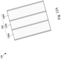
- the semiconductor device 10a includes a dual-gate trench type transistor 20a, in which the two gate electrodes 180a are linear and are parallelly arranged to co-control the channel region 150a.
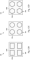
- the semiconductor devices such as semiconductor devices 10b-10g include a continuous-gate trench type transistor such as transistors 20a-20g.
- the channel region such as the channel region 150b-channel region 150g is continuously surrounded by the gate electrode such as the gate electrode 180b-gate electrode 180g.
- the channel region 150b-channel region 150d of the multiple transistors 20b-20d can be arranged in row and in column as a matric array.
- the channel region 150e-channel region 150e of the multiple transistors 20e-20g can be arranged in column, and the channel region 150e-channel region 150e of the multiple transistors 20e-20g in row can be misaligned.
- the shape of the channel region 150b-channel region 150g continuously surrounded by the gate electrode 180b-gate electrode 180g can be circle or polygon.
- the shape of the channel region 150b, channel region 150e in the transistors 20b, 20e can be a rectangle.
- the shape of the channel region 150c, channel region 150f in the transistors 20c, 20c can be a circle.
- the shape of the channel region 150d, channel region 150g in the transistors 20d, 20g can be a hexagon.
- Either the dual-gate trench type transistor 20a or the continuous-gate trench type transistors 20b-20g has advantage of improving conducting current and reduce on-current resistance.
- the disclosure provides a method of manufacturing semiconductor device and semiconductor device thereof.
- the shielding implant layer is formed at the bottom of the gate trench by using the self-aligned ion implantation process.
- the shielding implant layer disposed below the gate electrode and the gate oxide layer can reduce the bottom electric field of the gate oxide layer, so the gate oxide layer would be much reliable due to the electric field applied on the gate oxide layer would be lower than the breakdown voltage of the gate oxide layer.
- the oxidation rates at the sidewall and the bottom of the gate trench are not the same because of the self-aligned ion implantation process, so that the formed gate oxide layer has the bottom thickness not less than the sidewall thickness to further reduce the bottom electric field of the gate oxide layer of the semiconductor device having trench type gate.
- the method of manufacturing the semiconductor device of the disclosure includes using the self-aligned ion implantation process.
- the misalignment issue during the processes can be reduced, and the mask number utilized in the processes is reduced as well, the manufacturing complication and the cost can be reduced accordingly.
Landscapes
- Metal-Oxide And Bipolar Metal-Oxide Semiconductor Integrated Circuits (AREA)
- Electrodes Of Semiconductors (AREA)
Applications Claiming Priority (1)
| Application Number | Priority Date | Filing Date | Title |
|---|---|---|---|
| TW112107652A TWI832716B (zh) | 2023-03-02 | 2023-03-02 | 製作半導體裝置的方法與半導體裝置 |
Publications (2)
| Publication Number | Publication Date |
|---|---|
| EP4425565A2 true EP4425565A2 (de) | 2024-09-04 |
| EP4425565A3 EP4425565A3 (de) | 2024-09-18 |
Family
ID=90124078
Family Applications (1)
| Application Number | Title | Priority Date | Filing Date |
|---|---|---|---|
| EP24160704.3A Pending EP4425565A3 (de) | 2023-03-02 | 2024-02-29 | Verfahren zur herstellung eines halbleiterbauelements und halbleiterbauelement |
Country Status (3)
| Country | Link |
|---|---|
| US (1) | US20240297250A1 (de) |
| EP (1) | EP4425565A3 (de) |
| TW (1) | TWI832716B (de) |
Families Citing this family (1)
| Publication number | Priority date | Publication date | Assignee | Title |
|---|---|---|---|---|
| CN119562576B (zh) * | 2025-01-23 | 2025-05-09 | 通威微电子有限公司 | 一种mosfet元胞结构及其制作方法 |
Family Cites Families (9)
| Publication number | Priority date | Publication date | Assignee | Title |
|---|---|---|---|---|
| JP4903055B2 (ja) * | 2003-12-30 | 2012-03-21 | フェアチャイルド・セミコンダクター・コーポレーション | パワー半導体デバイスおよびその製造方法 |
| JPWO2010119789A1 (ja) * | 2009-04-13 | 2012-10-22 | ローム株式会社 | 半導体装置および半導体装置の製造方法 |
| JP5729331B2 (ja) * | 2011-04-12 | 2015-06-03 | 株式会社デンソー | 半導体装置の製造方法及び半導体装置 |
| JP6098417B2 (ja) * | 2013-07-26 | 2017-03-22 | 住友電気工業株式会社 | 炭化珪素半導体装置およびその製造方法 |
| JP6266975B2 (ja) * | 2013-12-26 | 2018-01-24 | トヨタ自動車株式会社 | 絶縁ゲート型半導体装置の製造方法及び絶縁ゲート型半導体装置 |
| JP6231396B2 (ja) * | 2014-02-10 | 2017-11-15 | トヨタ自動車株式会社 | 半導体装置及び半導体装置の製造方法 |
| CN110739344A (zh) * | 2019-10-24 | 2020-01-31 | 中芯集成电路制造(绍兴)有限公司 | 功率mos器件及其制造方法 |
| CN113241381B (zh) * | 2021-05-24 | 2024-05-14 | 厦门芯一代集成电路有限公司 | 一种高压槽栅mos器件及其制备方法 |
| CN114464680B (zh) * | 2022-01-04 | 2025-12-05 | 湖北九峰山实验室 | 碳化硅mosfet器件及其制作方法 |
-
2023
- 2023-03-02 TW TW112107652A patent/TWI832716B/zh active
-
2024
- 2024-02-29 EP EP24160704.3A patent/EP4425565A3/de active Pending
- 2024-03-01 US US18/592,541 patent/US20240297250A1/en active Pending
Also Published As
| Publication number | Publication date |
|---|---|
| US20240297250A1 (en) | 2024-09-05 |
| TW202437397A (zh) | 2024-09-16 |
| TWI832716B (zh) | 2024-02-11 |
| EP4425565A3 (de) | 2024-09-18 |
Similar Documents
| Publication | Publication Date | Title |
|---|---|---|
| US7834393B2 (en) | Semiconductor device and manufacturing method of the semiconductor device | |
| US7675126B2 (en) | Metal oxide semiconductor field effect transistor and method of fabricating the same | |
| US7301208B2 (en) | Semiconductor device and method for fabricating the same | |
| US8614482B2 (en) | Semiconductor power device having improved termination structure for mask saving | |
| EP1826815B1 (de) | Halbleiteranordnung und Verfahren zu deren Herstellung | |
| US8575702B2 (en) | Semiconductor device and method for fabricating semiconductor device | |
| US20020142529A1 (en) | Semiconductor device comprising buried channel region and method for manufacturing the same | |
| US5382536A (en) | Method of fabricating lateral DMOS structure | |
| EP1058303A1 (de) | Herstellung einer VDMOS-Struktur mit verminderten parasitären Effekten | |
| US8183632B2 (en) | Semiconductor device and method of manufacturing the same | |
| US6358783B1 (en) | Semiconductor device and method of manufacturing the same | |
| US20220165876A1 (en) | Semiconductor power devices having graded lateral doping and methods of forming such devices | |
| US12230697B2 (en) | Semiconductor device and method of manufacturing the same | |
| US11894440B2 (en) | Silicon carbide MOSFET device and manufacturing method thereof | |
| EP4425565A2 (de) | Verfahren zur herstellung eines halbleiterbauelements und halbleiterbauelement | |
| US8525256B2 (en) | Power semiconductor structure with schottky diode | |
| US12550397B2 (en) | Silicon carbide vertical conduction MOSFET device and manufacturing process thereof | |
| US20190279906A1 (en) | Semiconductor device and method for manufacturing the same | |
| US20250203977A1 (en) | Silicon carbide vertical conduction mosfet device for power applications and manufacturing process thereof | |
| KR20050028828A (ko) | 반도체 장치 및 그 제조방법 | |
| US20240234495A1 (en) | Gate trench power semiconductor devices having self-aligned trench shielding regions and related methods | |
| EP4036957A1 (de) | Vertikal leitende mosfet-vorrichtung aus siliziumkarbid für energieanwendungen und verfahren zur herstellung davon | |
| JP2021150405A (ja) | 炭化珪素半導体装置 | |
| KR100788367B1 (ko) | 이디모스 트랜지스터를 갖는 반도체 소자 및 그 형성 방법 | |
| US20230307528A1 (en) | Manufacturing method of forming semiconductor device and semiconductor device |
Legal Events
| Date | Code | Title | Description |
|---|---|---|---|
| PUAI | Public reference made under article 153(3) epc to a published international application that has entered the european phase |
Free format text: ORIGINAL CODE: 0009012 |
|
| STAA | Information on the status of an ep patent application or granted ep patent |
Free format text: STATUS: THE APPLICATION HAS BEEN PUBLISHED |
|
| REG | Reference to a national code |
Ref country code: DE Ref legal event code: R079 Free format text: PREVIOUS MAIN CLASS: H01L0029060000 Ipc: H01L0021336000 |
|
| PUAL | Search report despatched |
Free format text: ORIGINAL CODE: 0009013 |
|
| AK | Designated contracting states |
Kind code of ref document: A2 Designated state(s): AL AT BE BG CH CY CZ DE DK EE ES FI FR GB GR HR HU IE IS IT LI LT LU LV MC ME MK MT NL NO PL PT RO RS SE SI SK SM TR |
|
| AK | Designated contracting states |
Kind code of ref document: A3 Designated state(s): AL AT BE BG CH CY CZ DE DK EE ES FI FR GB GR HR HU IE IS IT LI LT LU LV MC ME MK MT NL NO PL PT RO RS SE SI SK SM TR |
|
| RIC1 | Information provided on ipc code assigned before grant |
Ipc: H01L 29/12 20060101ALI20240812BHEP Ipc: H01L 29/423 20060101ALI20240812BHEP Ipc: H01L 29/06 20060101ALI20240812BHEP Ipc: H01L 29/78 20060101ALI20240812BHEP Ipc: H01L 21/336 20060101AFI20240812BHEP |
|
| STAA | Information on the status of an ep patent application or granted ep patent |
Free format text: STATUS: REQUEST FOR EXAMINATION WAS MADE |
|
| 17P | Request for examination filed |
Effective date: 20250307 |