EP4404265A1 - Halbleiterbauelement und zugehörige schaltung, chip, elektronische vorrichtung und herstellungsverfahren - Google Patents
Halbleiterbauelement und zugehörige schaltung, chip, elektronische vorrichtung und herstellungsverfahren Download PDFInfo
- Publication number
- EP4404265A1 EP4404265A1 EP23778079.6A EP23778079A EP4404265A1 EP 4404265 A1 EP4404265 A1 EP 4404265A1 EP 23778079 A EP23778079 A EP 23778079A EP 4404265 A1 EP4404265 A1 EP 4404265A1
- Authority
- EP
- European Patent Office
- Prior art keywords
- region
- semiconductor layer
- igbt
- layer
- type
- Prior art date
- Legal status (The legal status is an assumption and is not a legal conclusion. Google has not performed a legal analysis and makes no representation as to the accuracy of the status listed.)
- Pending
Links
Images


Classifications
-
- H—ELECTRICITY
- H10—SEMICONDUCTOR DEVICES; ELECTRIC SOLID-STATE DEVICES NOT OTHERWISE PROVIDED FOR
- H10D—INORGANIC ELECTRIC SEMICONDUCTOR DEVICES
- H10D84/00—Integrated devices formed in or on semiconductor substrates that comprise only semiconducting layers, e.g. on Si wafers or on GaAs-on-Si wafers
- H10D84/60—Integrated devices formed in or on semiconductor substrates that comprise only semiconducting layers, e.g. on Si wafers or on GaAs-on-Si wafers characterised by the integration of at least one component covered by groups H10D10/00 or H10D18/00, e.g. integration of BJTs
- H10D84/611—Combinations of BJTs and one or more of diodes, resistors or capacitors
- H10D84/613—Combinations of vertical BJTs and one or more of diodes, resistors or capacitors
- H10D84/617—Combinations of vertical BJTs and only diodes
-
- H—ELECTRICITY
- H10—SEMICONDUCTOR DEVICES; ELECTRIC SOLID-STATE DEVICES NOT OTHERWISE PROVIDED FOR
- H10D—INORGANIC ELECTRIC SEMICONDUCTOR DEVICES
- H10D84/00—Integrated devices formed in or on semiconductor substrates that comprise only semiconducting layers, e.g. on Si wafers or on GaAs-on-Si wafers
- H10D84/80—Integrated devices formed in or on semiconductor substrates that comprise only semiconducting layers, e.g. on Si wafers or on GaAs-on-Si wafers characterised by the integration of at least one component covered by groups H10D12/00 or H10D30/00, e.g. integration of IGFETs
- H10D84/811—Combinations of field-effect devices and one or more diodes, capacitors or resistors
-
- H—ELECTRICITY
- H10—SEMICONDUCTOR DEVICES; ELECTRIC SOLID-STATE DEVICES NOT OTHERWISE PROVIDED FOR
- H10D—INORGANIC ELECTRIC SEMICONDUCTOR DEVICES
- H10D12/00—Bipolar devices controlled by the field effect, e.g. insulated-gate bipolar transistors [IGBT]
- H10D12/01—Manufacture or treatment
- H10D12/031—Manufacture or treatment of IGBTs
- H10D12/032—Manufacture or treatment of IGBTs of vertical IGBTs
- H10D12/038—Manufacture or treatment of IGBTs of vertical IGBTs having a recessed gate, e.g. trench-gate IGBTs
-
- H—ELECTRICITY
- H10—SEMICONDUCTOR DEVICES; ELECTRIC SOLID-STATE DEVICES NOT OTHERWISE PROVIDED FOR
- H10D—INORGANIC ELECTRIC SEMICONDUCTOR DEVICES
- H10D12/00—Bipolar devices controlled by the field effect, e.g. insulated-gate bipolar transistors [IGBT]
- H10D12/411—Insulated-gate bipolar transistors [IGBT]
- H10D12/418—Insulated-gate bipolar transistors [IGBT] having a drift region having a doping concentration that is higher at the emitter side relative to other parts of the drift region
-
- H—ELECTRICITY
- H10—SEMICONDUCTOR DEVICES; ELECTRIC SOLID-STATE DEVICES NOT OTHERWISE PROVIDED FOR
- H10D—INORGANIC ELECTRIC SEMICONDUCTOR DEVICES
- H10D12/00—Bipolar devices controlled by the field effect, e.g. insulated-gate bipolar transistors [IGBT]
- H10D12/411—Insulated-gate bipolar transistors [IGBT]
- H10D12/441—Vertical IGBTs
- H10D12/461—Vertical IGBTs having non-planar surfaces, e.g. having trenches, recesses or pillars in the surfaces of the emitter, base or collector regions
- H10D12/481—Vertical IGBTs having non-planar surfaces, e.g. having trenches, recesses or pillars in the surfaces of the emitter, base or collector regions having gate structures on slanted surfaces, on vertical surfaces, or in grooves, e.g. trench gate IGBTs
-
- H—ELECTRICITY
- H10—SEMICONDUCTOR DEVICES; ELECTRIC SOLID-STATE DEVICES NOT OTHERWISE PROVIDED FOR
- H10D—INORGANIC ELECTRIC SEMICONDUCTOR DEVICES
- H10D62/00—Semiconductor bodies, or regions thereof, of devices having potential barriers
- H10D62/10—Shapes, relative sizes or dispositions of the regions of the semiconductor bodies; Shapes of the semiconductor bodies
- H10D62/102—Constructional design considerations for preventing surface leakage or controlling electric field concentration
- H10D62/103—Constructional design considerations for preventing surface leakage or controlling electric field concentration for increasing or controlling the breakdown voltage of reverse-biased devices
- H10D62/105—Constructional design considerations for preventing surface leakage or controlling electric field concentration for increasing or controlling the breakdown voltage of reverse-biased devices by having particular doping profiles, shapes or arrangements of PN junctions; by having supplementary regions, e.g. junction termination extension [JTE]
- H10D62/109—Reduced surface field [RESURF] PN junction structures
- H10D62/111—Multiple RESURF structures, e.g. double RESURF or 3D-RESURF structures
-
- H—ELECTRICITY
- H10—SEMICONDUCTOR DEVICES; ELECTRIC SOLID-STATE DEVICES NOT OTHERWISE PROVIDED FOR
- H10D—INORGANIC ELECTRIC SEMICONDUCTOR DEVICES
- H10D62/00—Semiconductor bodies, or regions thereof, of devices having potential barriers
- H10D62/10—Shapes, relative sizes or dispositions of the regions of the semiconductor bodies; Shapes of the semiconductor bodies
- H10D62/124—Shapes, relative sizes or dispositions of the regions of semiconductor bodies or of junctions between the regions
- H10D62/126—Top-view geometrical layouts of the regions or the junctions
- H10D62/127—Top-view geometrical layouts of the regions or the junctions of cellular field-effect devices, e.g. multicellular DMOS transistors or IGBTs
-
- H—ELECTRICITY
- H10—SEMICONDUCTOR DEVICES; ELECTRIC SOLID-STATE DEVICES NOT OTHERWISE PROVIDED FOR
- H10D—INORGANIC ELECTRIC SEMICONDUCTOR DEVICES
- H10D62/00—Semiconductor bodies, or regions thereof, of devices having potential barriers
- H10D62/10—Shapes, relative sizes or dispositions of the regions of the semiconductor bodies; Shapes of the semiconductor bodies
- H10D62/13—Semiconductor regions connected to electrodes carrying current to be rectified, amplified or switched, e.g. source or drain regions
- H10D62/141—Anode or cathode regions of thyristors; Collector or emitter regions of gated bipolar-mode devices, e.g. of IGBTs
- H10D62/142—Anode regions of thyristors or collector regions of gated bipolar-mode devices
-
- H—ELECTRICITY
- H10—SEMICONDUCTOR DEVICES; ELECTRIC SOLID-STATE DEVICES NOT OTHERWISE PROVIDED FOR
- H10D—INORGANIC ELECTRIC SEMICONDUCTOR DEVICES
- H10D62/00—Semiconductor bodies, or regions thereof, of devices having potential barriers
- H10D62/10—Shapes, relative sizes or dispositions of the regions of the semiconductor bodies; Shapes of the semiconductor bodies
- H10D62/17—Semiconductor regions connected to electrodes not carrying current to be rectified, amplified or switched, e.g. channel regions
- H10D62/393—Body regions of DMOS transistors or IGBTs
-
- H—ELECTRICITY
- H10—SEMICONDUCTOR DEVICES; ELECTRIC SOLID-STATE DEVICES NOT OTHERWISE PROVIDED FOR
- H10D—INORGANIC ELECTRIC SEMICONDUCTOR DEVICES
- H10D64/00—Electrodes of devices having potential barriers
- H10D64/111—Field plates
- H10D64/117—Recessed field plates, e.g. trench field plates or buried field plates
-
- H—ELECTRICITY
- H10—SEMICONDUCTOR DEVICES; ELECTRIC SOLID-STATE DEVICES NOT OTHERWISE PROVIDED FOR
- H10D—INORGANIC ELECTRIC SEMICONDUCTOR DEVICES
- H10D8/00—Diodes
-
- H—ELECTRICITY
- H10—SEMICONDUCTOR DEVICES; ELECTRIC SOLID-STATE DEVICES NOT OTHERWISE PROVIDED FOR
- H10D—INORGANIC ELECTRIC SEMICONDUCTOR DEVICES
- H10D8/00—Diodes
- H10D8/01—Manufacture or treatment
- H10D8/045—Manufacture or treatment of PN junction diodes
-
- H—ELECTRICITY
- H10—SEMICONDUCTOR DEVICES; ELECTRIC SOLID-STATE DEVICES NOT OTHERWISE PROVIDED FOR
- H10D—INORGANIC ELECTRIC SEMICONDUCTOR DEVICES
- H10D8/00—Diodes
- H10D8/422—PN diodes having the PN junctions in mesas
-
- H—ELECTRICITY
- H10—SEMICONDUCTOR DEVICES; ELECTRIC SOLID-STATE DEVICES NOT OTHERWISE PROVIDED FOR
- H10D—INORGANIC ELECTRIC SEMICONDUCTOR DEVICES
- H10D84/00—Integrated devices formed in or on semiconductor substrates that comprise only semiconducting layers, e.g. on Si wafers or on GaAs-on-Si wafers
- H10D84/101—Integrated devices comprising main components and built-in components, e.g. IGBT having built-in freewheel diode
- H10D84/161—IGBT having built-in components
-
- H10P30/204—
-
- H10P30/21—
-
- H10P30/22—
-
- H—ELECTRICITY
- H10—SEMICONDUCTOR DEVICES; ELECTRIC SOLID-STATE DEVICES NOT OTHERWISE PROVIDED FOR
- H10D—INORGANIC ELECTRIC SEMICONDUCTOR DEVICES
- H10D62/00—Semiconductor bodies, or regions thereof, of devices having potential barriers
- H10D62/10—Shapes, relative sizes or dispositions of the regions of the semiconductor bodies; Shapes of the semiconductor bodies
- H10D62/128—Anode regions of diodes
Definitions
- the present invention relates to the field of semiconductor technologies, and in particular, to a power semiconductor device, a related circuit, a chip, an electronic device, and a preparation method.
- An insulated-gate bipolar field-effect transistor (insulated gate bipolar transistor, IGBT) is a complex fully controlled voltage-driven power semiconductor device including a bipolar junction transistor (bipolar junction transistor, BJT) and an insulated-gate field-effect transistor (metal-oxide-semiconductor field-effect transistor, MOSFET).
- BJT bipolar junction transistor
- MOSFET metal-oxide-semiconductor field-effect transistor
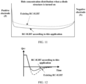
- FIG. 1A is a schematic top view of a chip before and after integration.
- FIG. 1B is a schematic cross-sectional view of an RC-IGBT chip.
- the RC-IGBT chips shown in FIG. 1A and FIG. 1B integrate functions of an IGBT and an FWD in a single-chip form, and two chips are converted into one chip.
- a total area of the chip can be reduced by about 20%, total costs of the chip can be reduced by about 15%, and power density of the devices can be increased by 20% in a same package size.
- an IGBT region and an FWD region may assist each other in heat dissipation, and thermal resistance can be reduced by about 30%, so that thermal performance of a system is improved.
- the foregoing N-channel IGBT is used as an example, and the RC-IGBT chip shown in FIG. 1B injects a large quantity of holes into a contact region in the FWD region. Consequently, excessive carriers are injected into a positive electrode of the FWD, resulting in a high reverse recovery loss of the FWD.
- Embodiments of the present invention provide a power semiconductor device, a related circuit, a chip, an electronic device, and a preparation method, to reduce a reverse recovery loss of a diode.
- an embodiment of this application provides a semiconductor device.
- the semiconductor device includes:
- the semiconductor device optimizes a front structure of the diode region, and reduces carrier concentration in the diode region by reducing a thickness of a semiconductor layer used as a positive electrode region or a negative electrode region in the region. In this way, front carrier injection efficiency when the diode is turned on is reduced, a reverse recovery charge amount when the diode is turned off is reduced, a reverse recovery loss Err is reduced, and switching efficiency of the RC-IGBT is finally improved.
- first-conductivity-type is N-type
- second-conductivity-type is P-type.
- Hole injection concentration in a positive electrode of the diode is reduced by reducing a thickness of a P-type second semiconductor layer in the region. In this way, a reverse recovery charge amount when the diode is turned off is reduced, a reverse recovery loss Err is reduced, and switching efficiency of the RC-IGBT is finally improved.
- first-conductivity-type is P-type
- second-conductivity-type is N-type. Electron injection concentration in a negative electrode of the diode is reduced by reducing a thickness of an N-type second semiconductor layer. In this way, a reverse recovery charge amount when the diode is turned off is reduced, and a reverse recovery loss Err of the diode is reduced.
- front in this embodiment of this application refers to a side, of the diode, near an emitter electrode.
- the front structure of the diode is the positive electrode region of the diode.
- the front structure of the diode is the negative electrode region of the diode.
- the thickness of the second semiconductor layer located in the IGBT region is 0.5 to 3 micrometers, and the thickness of the second semiconductor layer located in the diode region is 0.5 to 2.5 micrometers.
- a ratio of the thickness of the second semiconductor layer located in the diode region to the thickness of the second semiconductor layer located in the IGBT region is 0.2 to 0.8.
- the second semiconductor layer located in the IGBT region includes a second-conductivity-type contact region
- the semiconductor device includes a plurality of emitter regions disposed at intervals
- the contact region is disposed between two adjacent emitter regions
- second-conductivity-type impurity concentration in the contact region is greater than second-conductivity-type impurity concentration in the second semiconductor layer.
- the semiconductor device further optimizes the front structure of the diode region, and further reduces the carrier concentration in the diode region by removing the contact region in the diode region. In this way, the front carrier injection efficiency when the diode is turned on is reduced, the reverse recovery charge amount when the diode is turned off is further reduced, the reverse recovery loss Err is reduced, and the switching efficiency of the RC-IGBT is finally improved.
- the second semiconductor layer located in the diode region does not include a second-conductivity-type contact region.
- a difference between the thickness of the second semiconductor layer located in the IGBT region and the thickness of the second semiconductor layer located in the diode region is not less than a thickness of the contact region.
- the semiconductor device further includes:
- one end of the gate electrode is substantially flush with a surface, of the emitter region, away from the first semiconductor layer.
- the semiconductor device further includes:
- one end of the first electrode is substantially flush with the second semiconductor layer located in the diode region.
- a first-conductivity-type carrier storage CS layer is further included between the IGBT region and the second semiconductor layer or between the first semiconductor layer and the second semiconductor layer.
- the first semiconductor layer includes a first-conductivity-type pillar and a second-conductivity-type pillar that are arranged alternately along a first direction, the first direction is substantially perpendicular to a thickness direction, and both the first-conductivity-type pillar and the second-conductivity-type pillar extend along the thickness direction.
- an embodiment of this application further provides a power conversion circuit.
- the power conversion circuit includes at least the semiconductor device according to any one of the first aspect or the implementations of the first aspect.
- the power conversion circuit is a circuit configured to implement functions such as adjusting frequency conversion, conversion, phase change, rectification, inversion, and switching of a voltage/current, and may be an inverter circuit (inverter circuit), a rectifier (rectifier), a converter circuit, or the like.
- an embodiment of this application further provides a reverse conduction insulated gate bipolar transistor RC-IGBT chip.
- the RC-IGBT chip includes at least the semiconductor device according to any one of the first aspect or the implementations of the first aspect.
- an embodiment of this application further provides an electronic device.
- the electronic device includes at least the semiconductor device according to any one of the first aspect or the implementations of the first aspect; or includes at least the RC-IGBT chip according to any one of the third aspect or the implementations of the first aspect.
- an embodiment of this application further provides a semiconductor device preparation method.
- the method includes:
- a front structure of the diode region is optimized, and carrier concentration in the diode region is reduced by reducing a thickness of a semiconductor layer used as a positive electrode region or a negative electrode region in the region.
- front carrier injection efficiency when the diode is turned on is reduced, a reverse recovery charge amount when the diode is turned off is reduced, a reverse recovery loss Err is reduced, and switching efficiency of the RC-IGBT is finally improved.
- the thickness of the etched second semiconductor layer disposed in the IGBT region is 0.5 to 3 micrometers, and the thickness of the etched second semiconductor layer disposed in the diode region is 0.5 to 2.5 micrometers.
- a ratio of the thickness of the etched second semiconductor layer disposed in the diode region to the thickness of the etched second semiconductor layer disposed in the IGBT region is 0.2 to 0.8.
- the forming an emitter region and a contact region of the IGBT in the semiconductor layer disposed in the IGBT region includes:
- the forming an emitter region and a contact region of the IGBT in the semiconductor layer disposed in the IGBT region includes:
- the etching the semiconductor layer disposed in the diode region includes:
- the method further includes:
- the method further includes: forming a CS layer between the substrate and the semiconductor layer; or forming a CS layer between the substrate located in the IGBT region and the semiconductor layer.
- the method further includes: forming, in the substrate, a first-conductivity-type pillar and a second-conductivity-type pillar that are arranged alternately along a first direction, where the first direction is substantially perpendicular to a thickness direction, and both the first-conductivity-type pillar and the second-conductivity-type pillar extend along the thickness direction.
- the method further includes:
- the method further includes: etching the first electrode, the second insulation layer, and the insulation medium layer that are located in the diode region, where after the etching, one end of the first electrode and one end of the second insulation layer are both flush with the semiconductor layer located in the diode region.
- N (Negative)-type is electronic-type.
- a semiconductor that mainly performs electron conduction is referred to as the N-type semiconductor.
- the N-type semiconductor is obtained by doping an intrinsic semiconductor with a donor impurity.
- pure silicon is doped with a small quantity of pentavalent elements (phosphorus, arsenic, or the like). When the phosphorus forms a covalent bond with a surrounding tetravalent silicon atom, an extra free electron is generated.
- N-type may be further classified into N+ type (highly doped N-type) and N- type (lightly doped N-type), and impurity concentration in an N+ type semiconductor is greater than impurity concentration in an N- type semiconductor. It should be understood that N+ type (highly doped N-type) and N- type (lightly doped N-type) are relative to each other.
- P (Positive)-type is hole-type.
- a semiconductor that mainly performs hole conduction is referred to as the P-type semiconductor.
- the P-type semiconductor is obtained by doping an intrinsic semiconductor with an acceptor impurity.
- pure silicon is doped with a small quantity of trivalent elements (boron, indium, or the like). When the boron forms a covalent bond with a surrounding tetravalent silicon atom, there is a lack of an electron, resulting in a hole.
- P-type may be further classified into P+ type (highly doped P-type) and P- type (lightly doped P-type), and impurity concentration in a P+ type semiconductor is greater than impurity concentration in a P- type semiconductor.
- Insulated gate bipolar transistor insulated gate bipolar transistor, IGBT
- the IGBT is a complex fully controlled voltage-driven power semiconductor device including a bipolar junction transistor (bipolar junction transistor, BJT) and an insulated-gate field-effect transistor (metal-oxide-semiconductor field-effect transistor, MOSFET).
- BJT bipolar junction transistor
- MOSFET metal-oxide-semiconductor field-effect transistor
- the IGBT is applicable to a converter system with a direct current voltage of 600 V and above, such as an alternating current motor, a frequency converter, a switching power supply, a lighting circuit, traction drive, and other fields.
- Freewheeling diode freewheeling diode, FWD
- fast recovery diode fast recovery diode
- the FWD is a diode that freewheels when the IGBT is turned off in an inductive load switching circuit.
- the FRD is a diode having a fast reverse recovery speed.
- Reverse conduction IGBT Reverse conduction IGBT, RC-IGBT
- the RC-IGBT is an IGBT structure that integrates a diode that can freewheel when the IGBT is turned off.
- a first-generation IGBT is a punch through IGBT (punch through IGBT, PT-IGBT).
- the first-generation IGBT uses a planar gate structure, uses a thick P-type substrate with high doping concentration, and has an epitaxially growing N-type buffer and an epitaxially growing drift region.
- an electric field is distributed in a trapezoidal shape.
- the device has a low voltage withstand level, and a positive conduction voltage drop has a negative temperature characteristic, which is not conducive to parallel application.
- a second-generation IGBT is a non punch through IGBT (non punch through IGBT, NPT-IGBT).
- the second-generation IGBT has a groove gate structure, and uses a lightly doped N-type substrate as a drift layer.
- a back collector layer is formed by injecting a P-type impurity. During reverse blocking, an electric field is distributed in a triangle shape.
- the device has a greatly improved voltage withstand level. However, a substrate thickness is continuously increased, and a conduction voltage drop and a switching loss are both large.
- a third-generation IGBT is a field stop IGBT (Field stop IGBT, FS-IGBT).
- An N-type field stop layer is added on the basis of a structure of the second-generation IGBT.
- an electric field is distributed in a trapezoidal shape. In this way, a substrate thickness is reduced while a sufficient voltage withstand level of the device is ensured, so that both a conduction voltage drop and a switching loss are greatly reduced, and a compromise relationship between the conduction voltage drop Vcesat and a turn-off loss Eoff is improved.
- a fourth-generation IGBT is a refined FS-IGBT.
- the fourth-generation IGBT reduces a cell size, and optimizes back buffer distribution (for example, forms a deep buffer by injecting hydrogen), so that a substrate thickness is further reduced, and a compromise relationship between higher power density, a better conduction voltage drop Vcesat, and a turn-off loss Eoff is obtained.
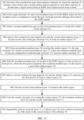
- FIG. 2A shows an equivalent circuit of an RC-IGBT.
- An integrated FWD of the RC-IGBT is connected in reverse parallel to an integrated IGBT, and performs a freewheeling function when the IGBT is turned off.
- FIG. 2B shows an IGBT region and an FWD region of the RC-IGBT device are switched alternately. Therefore, to reduce a switching loss of the RC-IGBT device, both a reverse recovery loss Err when the integrated FWD is turned off and a switching loss Eon and Eoff of the integrated IGBT need to be optimized.
- an injection enhancement technology is usually used to increase concentration of front carriers near an emitter region.
- etching of a contact region, injection of a P-type semiconductor layer, injection of a P contact region, and the like in a structure of an FWD region of an RC-IGBT are the same as those of an IGBT region.
- hole injection efficiency of a positive electrode region of an FWD is excessively high, and an excess carrier that needs to be extracted during reverse recovery, namely, a reverse recovery charge amount Qrr when the diode is turned off, is excessively large.
- a reverse recovery loss Err is excessively high, affecting switching efficiency of the RC-IGBT.
- the RC-IGBT optimizes a front structure of an FWD region, and reduces hole injection concentration in a positive electrode of an FWD by reducing a thickness of a P-type semiconductor layer in the region. In this way, front carrier injection efficiency when the diode is turned on is reduced, a reverse recovery charge amount when the diode is turned off is reduced, a reverse recovery loss Err of the diode is reduced, and switching efficiency of the RC-IGBT is finally improved.
- RC-IGBT including an N-type drift layer
- a positive electrode of an FWD is an N-type semiconductor layer. Electron injection concentration in a negative electrode of the FWD is reduced by reducing a thickness of the N-type semiconductor layer, so that a reverse recovery loss Err is reduced.
- the RC-IGBT may also be referred to as a semiconductor device, a power semiconductor device, or the like.
- the RC-IGBT may have a structure of a PT-IGBT, an NPT-IGBT, or an FS-IGBT.
- the PT-IGBT is of a planar gate type, and the NPT-IGBT and the FS-IGBT each are of a groove type.
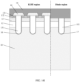
- FIG. 3A to FIG. 3C and FIG. 4 to FIG. 8 are schematic cross-sectional views of some RC-IGBTs according to embodiments of this application.
- the RC-IGBTs shown in FIG. 3A to FIG. 3C and FIG. 4 to FIG. 7 each are of a groove type, and the RC-IGBT shown in FIG. 8 is of a planar gate type.
- the RC-IGBT may include a part or all of structures of a first-conductivity-type first semiconductor layer 11, a first-conductivity-type carrier store (carrier store, CS) layer 12, a second-conductivity-type second semiconductor layer 13, a first-conductivity-type emitter region 131, a second-conductivity-type contact region 132, an emitter electrode 14, a gate electrode 151, a first electrode 152, a first insulation layer 16, a second insulation layer 17, an insulation medium layer 18, a buffer layer 19, a second-conductivity-type collector layer 20, a first-conductivity-type electrode layer 21, a collector electrode 22, and the like that are disposed in a stacked manner.
- CS carrier store
- first-conductivity-type is N-type and second-conductivity-type is P-type
- the electrode layer 21 belongs to a negative electrode of a diode. It may be understood that first-conductivity-type may alternatively be P-type, and second-conductivity-type may alternatively be N-type. In this case, the electrode layer 21 belongs to a positive electrode of a diode.
- the RC-IGBT may be divided into an IGBT region and a diode region.
- the diode is an FWD.
- the diode region is also referred to as an FWD region. It should be understood that the diode may alternatively be another type of diode.
- the IGBT region forms an IGBT device, and the FWD region forms an FWD.
- An N-channel IGBT is used as an example. An emitter electrode of the IGBT is shared with a positive electrode of the FWD, a Pbody layer of the IGBT is shared with a P region of the FWD, and an N-type drift layer of the IGBT is shared with an N region of the FWD.
- the N-type first semiconductor layer 11 is also referred to as an N-type drift layer or an N--type drift layer.
- the N-type drift layer includes a first surface and a second surface that are opposite to each other.
- the P-type second semiconductor layer 13 disposed on the first surface of the N-type first semiconductor layer 11 is also referred to as a Pbody layer, and is disposed on the first surface of the N-type drift layer.
- the P-type second semiconductor layer 13 may be formed by injecting a P-type impurity ion into the N-type drift layer or growing a P-type semiconductor.
- the P-type second semiconductor layer located in the IGBT region provides a channel when the IGBT works, and may also be referred to as a P-type channel layer; and the P-type second semiconductor layer located in the FWD region is a P region of the FWD, and is also referred to as a P region or a positive electrode region.
- a thickness d1 of the second semiconductor layer 13 located in the IGBT region is greater than a thickness d2 of the second semiconductor layer 13 located in the FWD region, to reduce carrier concentration in the second semiconductor layer 13 located in the FWD region.
- front carrier injection efficiency when the diode is turned on is reduced, a reverse recovery charge amount when the diode is turned off is reduced, a reverse recovery loss Err is reduced, and switching efficiency of the RC-IGBT is finally improved.
- the thickness of the second semiconductor layer 13 located in the IGBT region is 0.5 to 3 micrometers, and the thickness of the second semiconductor layer 13 located in the diode region is 0.5 to 2.5 micrometers.
- a ratio of the thickness of the second semiconductor layer 13 located in the diode region to the thickness of the second semiconductor layer 13 located in the IGBT region is 0.1 to 0.9 or 0.2 to 0.8.
- the ratio is 0.5 or 0.6.
- a plurality of emitter regions 131 disposed at intervals are disposed on a surface, of the second semiconductor layer 13, away from the first semiconductor layer 11.
- the emitter regions 131 exist only in the IGBT region.
- the N-type emitter region 131 may be obtained by injecting an N-type impurity ion into the second semiconductor layer 13 located on two sides of the gate electrode 151.
- the surface, of the second semiconductor layer 13, away from the first semiconductor layer 11 may include a plurality of contact regions 132.
- the contact region 132 may be located between two adjacent emitter regions 131, and is used for ohmic contact between the second semiconductor layer 13 and the emitter electrode 14. It may be understood that impurity ion concentration in the contact region 132 is usually higher than that in the second semiconductor layer 13.
- the emitter region 131 may be higher than the contact region 132 in a thickness direction.
- one end, of the emitter region 131, adjacent to the emitter electrode 14 may be substantially flush with one end, of the emitter region 131, adjacent to the emitter electrode 14.
- the "substantially flush with” means that a difference between average heights in a thickness direction is not large, for example, a difference is less than 1 nm.
- the contact region 132 exists only in the IGBT region.
- injection may be performed only in the IGBT region to form the contact region 132.
- a difference between the thickness of the second semiconductor layer 13 located in the IGBT region and the thickness of the second semiconductor layer 13 located in the FWD region is not less than a thickness of the contact region 132.
- a P-type impurity ion may be injected into a part of the P-type second semiconductor layer 13 located in the IGBT region and a part of the P-type second semiconductor layer 13 located in the FWD region, to form the contact region 132.
- the second semiconductor layer 13 and the contact region 132 that are located in the FWD region are etched under protection of the emitter region 131 by a mask, so that the contact region 132 located in the FWD region is completely etched. Therefore, carrier concentration in the positive electrode region in the FWD region is reduced, so that the reverse recovery charge amount and the reverse recovery loss Err are reduced.
- FIG. 9 is a schematic diagram of distribution of ohmic contact holes of the second semiconductor layer 13.
- the ohmic contact hole located in the IGBT region is formed by the contact region 132; and the contact region located in the IGBT region is formed by the second semiconductor layer 13 and the first electrode 152 in the region.
- the ohmic contact hole located in the IGBT region is narrower in width, and is located between the gate electrodes 151; and the ohmic contact hole located in the FWD region is wide in width, and the width of the ohmic contact hole is the width of the FWD region.
- the P-type second semiconductor layer 13 in the FWD region may include the contact region 132.
- a thickness d3 of the contact region 132 located in the FWD region may be less than a thickness d4 of the contact region 132 located in the IGBT region, so that carrier concentration in the contact region 132 located in the FWD region is reduced.
- a reverse recovery charge amount when the diode is turned off is reduced, a reverse recovery loss Err is reduced, and switching efficiency of the RC-IGBT is finally improved.
- the carrier storage (carrier store, CS) layer 12 may be further included between the N-type first semiconductor layer 11 and the P-type second semiconductor layer 13.
- the CS layer 12 exists in both the IGBT region and the FWD region.
- an impurity ion of a same conductivity type as the drift layer may be injected into the CS layer 12.
- the N-type CS layer 12 may form a hole barrier, to prevent the hole from being pulled out by the emitter when the IGBT is turned on, and improve injection efficiency of the drift layer near the emitter. In this way, conductivity modulation during conduction is increased, and a saturation voltage can be reduced.
- the CS layer 12 exists only in the IGBT region, and the first semiconductor layer 11 located in the FWD region is in direct contact with the second semiconductor layer 13 located in the FWD region. It should be understood that the CS layer 12 is not a necessary layer structure of the RC-IGBT. In some embodiments, the RC-IGBT may not include the CS layer.
- the groove-type RC-IGBTs shown in FIG. 3A to FIG. 3C and FIG. 4 to FIG. 7 each further include a plurality of gate electrodes 151, a first insulation layer 16, an insulation medium layer 18, and an emitter electrode 14.
- the plurality of gate electrodes 151 penetrate the second semiconductor layer 13 and the CS layer 12. One end of the gate electrode 151 is inserted into the first semiconductor layer 11 (drift layer).
- the first insulation layer 16 is included between each gate electrode 151 and each of the second semiconductor layer 13, the CS layer 12, and the first semiconductor layer 11.
- the other end of the gate electrode 151 is covered by the insulation medium layer 18.
- the RC-IGBT further includes the emitter electrode 14.
- the emitter electrode 14 is in contact with each emitter region 151 and each contact region 152.
- the insulation medium layer 18 is configured to isolate the gate electrode 151 from the emitter electrode 14.
- the insulation medium layer 18 may further cover or partially cover the emitter region 131, as shown in FIG. 3C .
- the emitter region 131 and the emitter electrode 14 may be electrically connected on a side surface of the device.
- the groove-type RC-IGBTs shown in FIG. 3A to FIG. 3C and FIG. 4 to FIG. 6 each further include at least one first electrode 152 and a second insulation layer 17.
- Each first electrode 152 penetrates the second semiconductor layer 13 and the CS layer 12.
- One end of the first electrode 152 is inserted into the first semiconductor layer 11 (drift layer).
- the second insulation layer 17 is included between each first electrode 152 and each of the second semiconductor layer 13, the CS layer 12, and the first semiconductor layer 11.
- the gate electrode 151 and the first electrode 152 may be generated by using a same process.
- An electrode located in the IGBT region is referred to as the gate electrode 151
- an electrode located in the FWD region is referred to as the first electrode 152.
- the first electrode 152 located in the FWD region is also etched, so that the other end of the first electrode 152 is flush with the second semiconductor layer 13 located in the FWD region.
- the first electrode 152 located in the FWD region may alternatively not be etched. This is not limited herein.
- the first electrode 152 located in the FWD region is electrically connected to the emitter electrode 14, and may function as a positive electrode.
- the FWD region may not include the first electrode 152 and the second insulation layer 17.
- the RC-IGBT further includes a buffer layer 19 (also referred to as a field stop layer), a collector layer 20, and an electrode layer 21 that are disposed on the second surface of the first semiconductor layer 11.
- a buffer layer 19 also referred to as a field stop layer
- the buffer layer 19 and the first semiconductor layer 11 are of a same conductivity type, and impurity ion concentration in the buffer layer 19 is greater than that in the first semiconductor layer. Therefore, for the N-type first semiconductor, the buffer layer 19 is also referred to as an N+ type buffer layer or an N+ type field stop layer.
- the buffer layer 19 is not a necessary layer structure, and both the collector layer 20 and the electrode layer 21 are configured to provide ohmic contact.
- an N-type pillar 111 and a P-type pillar 112 that are arranged alternately along a first direction are disposed on the first-conductivity-type first semiconductor layer 11, and both the N-type pillar 111 and the P-type pillar 112 extend along a thickness direction of the first semiconductor layer 11, to form a structure of a super-junction drift region.
- the N-type pillar 111 and the P-type pillar 112 are exhausted each other, which is equivalent to reducing effective doping concentration in the drift region, so that a voltage withstand level of the device is improved.
- the first direction is perpendicular or substantially perpendicular to the thickness direction of the device. It should be understood that “substantially perpendicular” may be regarded as that an angle is about 90°. For example, an angle range is 85° to 105° or 80° to 110°.
- the first semiconductor layer 11 of the device includes grooves disposed at intervals.
- the P-type second semiconductor layer 13 is disposed in the grooves.
- the P-type second semiconductor layer 13 located in the grooves is referred to as a P well region.
- An N+ type emitter region 131 and a P+ type contact region 132 are disposed in the P well region located in the IGBT region.
- the gate electrodes 151 are disposed on the first surface of the first semiconductor layer 11 at intervals, and a first insulation layer 16 is included between the gate electrode 151 and the first semiconductor layer 11.
- a thickness d1 of the second semiconductor layer 13 located in the IGBT region is greater than a thickness d2 of the second semiconductor layer 13 located in the FWD region, and the second semiconductor layer 13 located in the FWD region does not include the contact region 132, to reduce carrier concentration in the second semiconductor layer 13 located in the FWD region.
- front carrier injection efficiency when the diode is turned on is reduced, a reverse recovery charge amount when the FWD is turned off is reduced, a reverse recovery loss Err is reduced, and switching efficiency of the RC-IGBT is finally improved.
- a channel that conducts the emitter region and the first semiconductor layer may be formed at a position, of the second semiconductor layer 13, adjacent to the gate electrode.
- an N-channel RC-IGBT is used as an example to compare schematic cross-sectional views of an FWD region of an RC-IGBT in a conventional technology and an FWD region of an RC-IGBT according to an embodiment of this application.
- a collector electrode located in the FWD region is also referred to as a negative electrode
- an emitter electrode located in the FWD region is also referred to as a positive electrode.
- a thickness d1 of a P-type semiconductor layer in the FWD region is equal to that in an IGBT region, and is greater than a thickness d2 of a P-type semiconductor layer in the FWD region of the RC-IGBT according to this embodiment of this application.
- an etching depth t1 of the P-type semiconductor layer in the conventional technology may be less than an etching depth t2 of the P-type semiconductor layer in this embodiment of this application.
- etching performed on the P-type semiconductor layer in this embodiment of this application may be etching performed on the entire FWD region, to reduce carrier concentration in the P-type semiconductor layer in the FWD region. In this way, a reverse recovery charge amount Qrr when the diode is turned off is reduced, a reverse recovery loss Err is reduced, and switching efficiency of the RC-IGBT is finally improved.
- FIG. 11 is a schematic diagram of drift layer hole concentration distribution of an existing RC-IGBT and an RC-IGBT according to this application when an FWD is turned on. It can be learned that, when the FWD is turned on, the drift layer hole concentration in the RC-IGBT according to this application is less than that in the existing RC-IGBT.
- FIG. 12 is a schematic illustrative diagram of reverse recovery charge amounts Qrr of an existing RC-IGBT and an RC-IGBT according to this application when an FWD is turned off. It can be learned that, when the FWD is turned off, the reverse recovery charge amount Qrr of the RC-IGBT according to this application is less than that of the existing RC-IGBT.
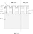
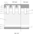
- FIG. 13 is a schematic flowchart of an RC-IGBT preparation method. As shown in FIG. 13 and FIG. 14A to FIG. 14H , the preparation method may include but is not limited to a part or all of the following steps.
- S01 Provide a first-conductivity-type semiconductor substrate 10, where the substrate 10 includes a first surface and a second surface that are opposite to each other, and may be divided into a region used to form an IGBT and a region used to form a diode, which are referred to as an IGBT region and a diode region respectively.
- the substrate 10 corresponds to the first semiconductor layer 11 in the RC-IGBT, and is a drift layer of the device after preparation.
- an N-type pillar and a P-type pillar that are arranged alternately along a first direction may be formed in the substrate 10, to form a structure of a super-junction drift region.
- the first direction is perpendicular or substantially perpendicular to a thickness direction of the device, and both the N-type pillar and the P-type pillar extend along the thickness direction.
- S02 Form a gate electrode 151 and a first insulation layer 16 of the IGBT, where the first insulation layer is configured to isolate the gate electrode from the substrate 10 located in the IGBT region.
- the substrate 10 may be etched by using a photoetching process, to form a plurality of grooves, where the grooves are used to expose the substrate 10. Then, a first insulation material and a first metal are sequentially deposited in the grooves.
- the first metal located in the IGBT region is referred to as the gate electrode 151, and the first insulation material located between the gate electrode 151 and the substrate 10 is the first insulation layer 16; and the first metal located in the diode region is referred to as a first electrode 152, and the first insulation material located between the first electrode 152 and the substrate 10 is a second insulation layer 17.
- first electrode 152 and the second insulation layer 17 are not necessary structures of the RC-IGBT. In some other embodiments, the first electrode 152 and the second insulation layer 17 may not be formed.
- a first insulation material and a first metal may be sequentially deposited on the first surface of the substrate 10, to form a first insulation material layer and a first metal layer that are sequentially stacked on a second semiconductor layer. Then, the first insulation material layer and the first metal layer are patterned by using a photoetching process, to obtain the gate electrode, the first insulation layer, the first electrode, and the second insulation layer.
- the first metal layer located in the IGBT region is referred to as the gate electrode, and the first insulation material located between the gate electrode and the substrate 10 is the first insulation layer; and the first metal layer located in the diode region is referred to as a first electrode, and the first insulation material layer located between the first electrode and the substrate 10 is a second insulation layer.
- a first-conductivity-type impurity ion and a second-conductivity-type impurity ion may be injected into two sides of the gate electrode 151 on the first surface of the substrate 10.
- An injection depth of the first-conductivity-type impurity ion is greater than that of the second-conductivity-type impurity ion.
- a region in which the first-conductivity-type impurity ion is injected into the substrate 10 is the CS layer
- a region in which the second-conductivity-type impurity ion is injected into the substrate 10 is a second semiconductor layer 13.
- the CS layer 12 is not a necessary layer structure of the RC-IGBT. In some other embodiments, the CS layer 12 may not be formed.
- the first-conductivity-type impurity ion may be injected only into the substrate 10 located in the IGBT region. That is, the CS layer 12 is formed only in the IGBT region.
- a second-conductivity-type impurity ion may be injected into a plurality of regions on the first surface of the substrate 10, to form a plurality of second-conductivity-type well regions, where the plurality of second-conductivity-type well regions are the second semiconductor layer.
- the CS layer 12 and the second semiconductor layer 13 may be sequentially deposited and grown on the first surface of the substrate 10, and then the groove-type gate electrode 151 and the groove-type first electrode 152 are formed.
- S04 Inject the first-conductivity-type impurity ion into the second semiconductor layer 13 located on two sides of the gate electrode 151, to form an emitter region 131.
- the first-conductivity-type impurity ion may be injected only into a surface of the second semiconductor layer 13 located in the IGBT region, to form the emitter region 131.
- a thickness of the emitter region 131 is less than a thickness of the second semiconductor layer 13.
- S05 Form an insulation medium layer 18 covering the emitter region 131, the gate electrode 151, and the second semiconductor layer 13, where the insulation medium layer 18 may be configured to isolate the gate electrode 151 from the emitter electrode 14, as shown in FIG. 14D .
- S06 Etch the insulation medium layer 18 located in the IGBT region, to form at least one first groove, where the first groove penetrates the insulation medium layer 18 and exposes a part of the emitter region 131, as shown in FIG. 14D and FIG. 14E .
- a first photoresist layer covering the insulation medium layer 18 may be first formed, and the first photoresist layer is partially exposed by using a light cover, to form a first mask.
- the first mask is configured to protect the insulation medium layer 18. Further, the insulation medium layer 18 exposed by the first mask is etched to a first depth, to form the first groove.
- the second-conductivity-type impurity ion may be injected into a surface of the second semiconductor layer 13 that is located in the IGBT region and that is exposed in the first groove, to form the contact region 132.
- the contact region 132 is located only in the IGBT region.
- S08 Etch the second semiconductor layer 13 located in the diode region, as shown in FIG. 14G and FIG. 14H .
- a second photoresist layer covering the contact region 132 and the insulation medium layer may be first formed, and the second photoresist layer is partially exposed by using a light cover, to form a second mask.
- the second mask is configured to protect the emitter region 131, the contact region 132, the insulation medium layer 18, and the like that are located in the IGBT region.
- the insulation medium layer 18 and the second semiconductor layer 13 that are located in the diode region and that are exposed by the second mask are etched, to reduce a thickness of the second semiconductor layer 13 in the diode region. It should be understood that, when the diode region includes the first electrode 152 and the second insulation layer 17, the first electrode 152 and the second insulation layer 17 may also be etched.
- One end, of the etched first electrode, adjacent to the emitter electrode 14 and one end, of the etched second insulation layer 17, adjacent to the emitter electrode 14 both are substantially flush with an etched semiconductor layer located in the diode region or higher than the etched semiconductor layer located in the diode region.
- S09 Form the emitter electrode 14 covering the contact region 132, the insulation medium layer 18, and the second semiconductor layer 13, as shown in FIG. 14I .
- the insulation medium layer 18 located on a surface of the emitter region 131 may also be etched off, so that the emitter region 131 is in contact with the emitter electrode 14, to implement an electrical connection between the emitter region 131 and the emitter electrode 14.
- the emitter region 131 When the emitter region 131 is isolated from the emitter electrode 14 by the insulation medium layer 18, the emitter region 131 and the emitter electrode 14 may be electrically connected on a side surface of the device.
- S 10 Sequentially form an electrode layer 21, a collector layer 20, and a collector electrode 22 of the diode on the second surface of the substrate 10, as shown in FIG. 14J .
- the first-conductivity-type impurity ion may be injected into the second surface of the substrate 10, to form a buffer layer 19.
- the second-conductivity-type impurity ion may be further injected into the IGBT region, to form the collector layer 20, and the first-conductivity-type impurity ion may further be injected into the diode region, to form the electrode layer 21.
- impurity ion concentration in the buffer layer 19 is greater than that in the substrate 10.
- An injection depth of the impurity ion forming the buffer layer 19 is greater than injection depths of the impurity ions forming the collector layer 20 and the electrode layer 21, to form a structure shown in FIG. 14J . Further, a metal layer covering the electrode layer 21 and the collector layer 20 is formed, to obtain the collector electrode 22.
- buffer layer 19 the electrode layer 21, and the collector layer 20 may be further included.
- a buffer layer, a second electrode layer, and a collector layer are grown on the surface of the substrate 10.
- the buffer layer 19 is not a necessary layer structure of the RC-IGBT. In some other embodiments, the buffer layer 19 may not be included.
- the insulation medium layer 18 and a part of the emitter region 131 that are located in the IGBT region may be etched, to form at least one second groove.
- the second groove penetrates the insulation medium layer 18 and the emitter region 131, and is configured to expose the second semiconductor layer 13, to obtain a semiconductor structure shown in FIG. 15A .
- the second-conductivity-type impurity ion is injected into the second semiconductor layer 13 exposed in the second groove, to form the contact region 132, as shown in FIG. 15B and FIG. 15C .
- S08 is sequentially performed, to obtain a semiconductor structure shown in FIG. 15E .
- An etching depth L1 of the second groove located in the IGBT region is less than an etching depth L2 of a layer structure located in the diode region. Because the to-be-etched insulation medium layers 18 have a same thickness, an etching depth of the emitter region 131 located in the IGBT region is less than an etching depth of the second semiconductor layer 13 located in the diode region, so that a thickness of the second semiconductor layer 13 in the diode region is reduced, and then carrier concentration in the diode region is reduced. In this way, front carrier injection efficiency when the diode is turned on is reduced, a reverse recovery charge amount when the diode is turned off is reduced, a reverse recovery loss Err is reduced, and switching efficiency of the RC-IGBT is finally improved.
- a structure shown in FIG. 15F may be obtained by performing S09, and then a structure shown in FIG. 15G may be obtained by performing S 10.
- the light cover and the process for preparing an IGBT may be used as much as possible.
- a contact region may also be formed in a diode region.
- etching is performed in step S08, partial etching or complete etching is performed on the contact region of the diode region.
- a structure shown in FIG. 16A is formed by using an IGBT forming process in the conventional technology. Further, the insulation medium layer 18, the emitter region 131, the contact region 132, the second semiconductor layer 13, the first electrode 152, and the second insulation layer 17 that are located in the diode region may be etched, to form a structure shown in FIG. 16B . In this way, the electrode layer 21, the collector layer 20, and the collector electrode 22 of the diode are sequentially formed on the second surface of the substrate 10, as shown in FIG. 16C .
- first-conductivity-type is N-type and second-conductivity-type is P-type
- the electrode layer is a negative electrode region of the diode
- first-conductivity-type is P-type and second-conductivity-type is N-type
- the electrode layer is a positive electrode region of the diode
- the foregoing layer structures may be prepared by using a combination of a photolithography technology and a thin film preparation technology. This is not limited herein. This is not limited to the schematic diagrams of the preparation procedures shown in FIG. 14A to FIG. 14E , and another structure and another preparation method may be further included. This is not limited in this embodiment of this application.
- the RC-IGBT is used as an energy conversion and transmission circuit, for example, used for frequency conversion, conversion, phase change, rectification, inversion, and switching of a voltage/current.
- the RC-IGBT device may be encapsulated as a power module, for example, an IGBT discrete device, an IGBT module, and an intelligent power module (intelligent power module, IPM).
- the IGBT discrete device may be the foregoing RC-IGBT chip.
- the IGBT module is obtained by packaging one or more RC-IGBT chips into a DBC substrate through insulation.
- the IPM is a "combined" device obtained by integrating the RC-IGBT device with peripheral circuits such as a drive circuit, an over-voltage and over-current protection circuit, and a temperature monitoring and over-temperature protection circuit.
- the RC-IGBT may be used as a power conversion circuit implementing functions such as adjusting frequency conversion, conversion, phase change, rectification, inversion, and switching of a voltage/current, for example, an inverter circuit (inverter circuit), a rectifier (rectifier), or a converter circuit.
- inverter circuit inverter circuit
- rectifier rectifier
- the boost converter is also referred to as a boost converter, and is a direct current-direct current converter that can step up a voltage.
- An output (a load) voltage of the boost converter is greater than an input (a power supply) voltage.
- the boost converter mainly includes switching power supplies of at least one diode, at least one transistor, and at least one energy storage element (inductor).
- the IGBT device provided in this application may be used as a transistor.
- the buck converter is also referred to as a buck converter, and is a direct current-direct current converter that can step down a voltage.
- An output (a load) voltage of the buck converter is less than an input (a power supply) voltage, but an output current of the buck converter is greater than an input current.
- the buck converter mainly includes at least one diode, at least one transistor, and at least one energy storage element (a capacitor, an inductor, or both).
- a filter that mainly includes a capacitor may be further added at an output end and an input end to reduce a voltage ripple.
- the IGBT device provided in this application may be used as a transistor.
- a voltage of a solar panel constantly changes due to a time or weather change.
- the boost converter is added to a photovoltaic inverter, to regulate a voltage that is input to an inverter circuit, so that electric energy emitted by a solar cell is provided to an alternating current grid.
- the semiconductor device that is provided in this application and that is used as a switching device may be used in another circuit that requires a power semiconductor device, for example, a direct current boost circuit or a direct current buck circuit. This is not limited herein.
- the RC-IGBT or the circuit or the device including the RC-IGBT may be further used in a vehicle such as an electric vehicle or a subway vehicle, or may be used in a home appliance such as a variable frequency air conditioner or a variable frequency refrigerator, or may be used in a photovoltaic device or the like.
Landscapes
- Physics & Mathematics (AREA)
- High Energy & Nuclear Physics (AREA)
- Engineering & Computer Science (AREA)
- Metal-Oxide And Bipolar Metal-Oxide Semiconductor Integrated Circuits (AREA)
- Toxicology (AREA)
- Health & Medical Sciences (AREA)
- Condensed Matter Physics & Semiconductors (AREA)
- General Physics & Mathematics (AREA)
- Manufacturing & Machinery (AREA)
- Computer Hardware Design (AREA)
- Microelectronics & Electronic Packaging (AREA)
- Power Engineering (AREA)
- Composite Materials (AREA)
- Chemical & Material Sciences (AREA)
Applications Claiming Priority (2)
| Application Number | Priority Date | Filing Date | Title |
|---|---|---|---|
| CN202210327363.0A CN116936573A (zh) | 2022-03-30 | 2022-03-30 | 半导体器件及相关电路、芯片、电子设备、制备方法 |
| PCT/CN2023/084016 WO2023185712A1 (zh) | 2022-03-30 | 2023-03-27 | 半导体器件及相关电路、芯片、电子设备、制备方法 |
Publications (2)
| Publication Number | Publication Date |
|---|---|
| EP4404265A1 true EP4404265A1 (de) | 2024-07-24 |
| EP4404265A4 EP4404265A4 (de) | 2025-03-05 |
Family
ID=88199343
Family Applications (1)
| Application Number | Title | Priority Date | Filing Date |
|---|---|---|---|
| EP23778079.6A Pending EP4404265A4 (de) | 2022-03-30 | 2023-03-27 | Halbleiterbauelement und zugehörige schaltung, chip, elektronische vorrichtung und herstellungsverfahren |
Country Status (4)
| Country | Link |
|---|---|
| US (1) | US20240282767A1 (de) |
| EP (1) | EP4404265A4 (de) |
| CN (1) | CN116936573A (de) |
| WO (1) | WO2023185712A1 (de) |
Families Citing this family (3)
| Publication number | Priority date | Publication date | Assignee | Title |
|---|---|---|---|---|
| CN117650161B (zh) * | 2023-10-31 | 2024-08-16 | 海信家电集团股份有限公司 | 半导体装置和半导体装置的制造方法 |
| CN120435017A (zh) * | 2024-02-01 | 2025-08-05 | 华为技术有限公司 | 半导体器件及相关电路、芯片、电子设备、制备方法 |
| CN120343935B (zh) * | 2025-06-19 | 2025-09-05 | 成都森未科技有限公司 | 超结igbt器件及其制备方法 |
Family Cites Families (5)
| Publication number | Priority date | Publication date | Assignee | Title |
|---|---|---|---|---|
| JP5103830B2 (ja) * | 2006-08-28 | 2012-12-19 | 三菱電機株式会社 | 絶縁ゲート型半導体装置 |
| JP2010171057A (ja) * | 2009-01-20 | 2010-08-05 | Denso Corp | 半導体装置およびその製造方法 |
| CN103489908A (zh) * | 2013-09-16 | 2014-01-01 | 电子科技大学 | 一种能消除负阻效应的rc-igbt |
| CN109860284B (zh) * | 2019-01-24 | 2022-06-03 | 安建科技(深圳)有限公司 | 一种逆导型绝缘栅双极性晶体管结构及其制备方法 |
| CN113990926B (zh) * | 2021-10-26 | 2023-11-24 | 电子科技大学 | 一种降低集成二极管反向恢复损耗的rc-igbt结构 |
-
2022
- 2022-03-30 CN CN202210327363.0A patent/CN116936573A/zh active Pending
-
2023
- 2023-03-27 WO PCT/CN2023/084016 patent/WO2023185712A1/zh not_active Ceased
- 2023-03-27 EP EP23778079.6A patent/EP4404265A4/de active Pending
-
2024
- 2024-04-29 US US18/649,460 patent/US20240282767A1/en active Pending
Also Published As
| Publication number | Publication date |
|---|---|
| US20240282767A1 (en) | 2024-08-22 |
| EP4404265A4 (de) | 2025-03-05 |
| WO2023185712A1 (zh) | 2023-10-05 |
| CN116936573A (zh) | 2023-10-24 |
Similar Documents
| Publication | Publication Date | Title |
|---|---|---|
| EP4404265A1 (de) | Halbleiterbauelement und zugehörige schaltung, chip, elektronische vorrichtung und herstellungsverfahren | |
| US11646369B2 (en) | Silicon carbide semiconductor device having a conductive layer formed above a bottom surface of a well region so as not to be in ohmic connection with the well region and power converter including the same | |
| CN114188396B (zh) | 一种绝缘栅双极晶体管及其制造方法、电子设备 | |
| EP4113624B1 (de) | Halbleitervorrichtung und zugehöriger chip und herstellungsverfahren | |
| JP4167313B2 (ja) | 高耐圧電力用半導体装置 | |
| US12527045B2 (en) | Semiconductor device, and related module, circuit, and preparation method | |
| JPH08316479A (ja) | 絶縁ゲート型半導体装置およびその製造方法 | |
| EP2667418B1 (de) | Halbleiterbauelement | |
| CN101694850A (zh) | 一种具有p型浮空层的载流子存储槽栅igbt | |
| CN118156264A (zh) | 一种功率半导体器件及功率转换电路、制备方法 | |
| JP2010251608A (ja) | 半導体装置 | |
| CN113725280A (zh) | 一种低开启电压的超结rb-igbt器件 | |
| CN215731726U (zh) | 一种低开启电压的超结rb-igbt器件 | |
| Zhou et al. | 4H-SiC trench MOSFET with integrated heterojunction diode for optimizing switching performance | |
| US20150349102A1 (en) | Ti-igbt and formation method thereof | |
| Noguchi et al. | RC-IGBT for Mild Hybrid Electric Vehicles | |
| CN120435017A (zh) | 半导体器件及相关电路、芯片、电子设备、制备方法 | |
| JPH0758328A (ja) | 自己消弧型半導体装置 | |
| Chen et al. | A New Double Trench SiC MOSFET Integrated Multifunctional Gates for Improved Reverse Conduction Performance | |
| CN118156295A (zh) | 一种含有n+阱区的混合集电极结构高温igbt器件 | |
| EP4109559A1 (de) | Bipolartransistor mit isolierter steuerelektrode, motorsteuereinheit für ein kraftfahrzeug | |
| KR20250163252A (ko) | 전력반도체 소자 및 이를 포함하는 전력변환 장치 | |
| KR20230165511A (ko) | 스냅백 현상을 억제하기 위한 구조를 갖는 rc igbt | |
| CN121126851A (zh) | 一种逆导型绝缘栅双极性晶体管及其制备方法 | |
| CN118943174A (zh) | 一种可快速关断的igbt器件及其制作方法 |
Legal Events
| Date | Code | Title | Description |
|---|---|---|---|
| STAA | Information on the status of an ep patent application or granted ep patent |
Free format text: STATUS: THE INTERNATIONAL PUBLICATION HAS BEEN MADE |
|
| PUAI | Public reference made under article 153(3) epc to a published international application that has entered the european phase |
Free format text: ORIGINAL CODE: 0009012 |
|
| STAA | Information on the status of an ep patent application or granted ep patent |
Free format text: STATUS: REQUEST FOR EXAMINATION WAS MADE |
|
| 17P | Request for examination filed |
Effective date: 20240419 |
|
| AK | Designated contracting states |
Kind code of ref document: A1 Designated state(s): AL AT BE BG CH CY CZ DE DK EE ES FI FR GB GR HR HU IE IS IT LI LT LU LV MC ME MK MT NL NO PL PT RO RS SE SI SK SM TR |
|
| REG | Reference to a national code |
Ref country code: DE Ref legal event code: R079 Free format text: PREVIOUS MAIN CLASS: H01L0027070000 Ipc: H01L0021265000 |
|
| A4 | Supplementary search report drawn up and despatched |
Effective date: 20250131 |
|
| RIC1 | Information provided on ipc code assigned before grant |
Ipc: H10D 84/80 20250101ALI20250127BHEP Ipc: H10D 64/00 20250101ALI20250127BHEP Ipc: H10D 62/17 20250101ALI20250127BHEP Ipc: H10D 84/00 20250101ALI20250127BHEP Ipc: H10D 62/10 20250101ALI20250127BHEP Ipc: H10D 12/00 20250101ALI20250127BHEP Ipc: H10D 12/01 20250101ALI20250127BHEP Ipc: H10D 8/00 20250101ALI20250127BHEP Ipc: H01L 21/265 20060101AFI20250127BHEP |
|
| DAV | Request for validation of the european patent (deleted) | ||
| DAX | Request for extension of the european patent (deleted) |