EP4383462A1 - Leiteranschlussmodul - Google Patents
Leiteranschlussmodul Download PDFInfo
- Publication number
- EP4383462A1 EP4383462A1 EP23214614.2A EP23214614A EP4383462A1 EP 4383462 A1 EP4383462 A1 EP 4383462A1 EP 23214614 A EP23214614 A EP 23214614A EP 4383462 A1 EP4383462 A1 EP 4383462A1
- Authority
- EP
- European Patent Office
- Prior art keywords
- contact
- conductor connection
- connection module
- circuit board
- insulating housing
- Prior art date
- Legal status (The legal status is an assumption and is not a legal conclusion. Google has not performed a legal analysis and makes no representation as to the accuracy of the status listed.)
- Pending
Links
Images











Classifications
-
- H—ELECTRICITY
- H01—ELECTRIC ELEMENTS
- H01R—ELECTRICALLY-CONDUCTIVE CONNECTIONS; STRUCTURAL ASSOCIATIONS OF A PLURALITY OF MUTUALLY-INSULATED ELECTRICAL CONNECTING ELEMENTS; COUPLING DEVICES; CURRENT COLLECTORS
- H01R12/00—Structural associations of a plurality of mutually-insulated electrical connecting elements, specially adapted for printed circuits, e.g. printed circuit boards [PCB], flat or ribbon cables, or like generally planar structures, e.g. terminal strips, terminal blocks; Coupling devices specially adapted for printed circuits, flat or ribbon cables, or like generally planar structures; Terminals specially adapted for contact with, or insertion into, printed circuits, flat or ribbon cables, or like generally planar structures
- H01R12/50—Fixed connections
- H01R12/51—Fixed connections for rigid printed circuits or like structures
- H01R12/515—Terminal blocks providing connections to wires or cables
-
- H—ELECTRICITY
- H01—ELECTRIC ELEMENTS
- H01R—ELECTRICALLY-CONDUCTIVE CONNECTIONS; STRUCTURAL ASSOCIATIONS OF A PLURALITY OF MUTUALLY-INSULATED ELECTRICAL CONNECTING ELEMENTS; COUPLING DEVICES; CURRENT COLLECTORS
- H01R12/00—Structural associations of a plurality of mutually-insulated electrical connecting elements, specially adapted for printed circuits, e.g. printed circuit boards [PCB], flat or ribbon cables, or like generally planar structures, e.g. terminal strips, terminal blocks; Coupling devices specially adapted for printed circuits, flat or ribbon cables, or like generally planar structures; Terminals specially adapted for contact with, or insertion into, printed circuits, flat or ribbon cables, or like generally planar structures
- H01R12/70—Coupling devices
- H01R12/7005—Guiding, mounting, polarizing or locking means; Extractors
- H01R12/7011—Locking or fixing a connector to a PCB
- H01R12/707—Soldering or welding
-
- H—ELECTRICITY
- H01—ELECTRIC ELEMENTS
- H01R—ELECTRICALLY-CONDUCTIVE CONNECTIONS; STRUCTURAL ASSOCIATIONS OF A PLURALITY OF MUTUALLY-INSULATED ELECTRICAL CONNECTING ELEMENTS; COUPLING DEVICES; CURRENT COLLECTORS
- H01R25/00—Coupling parts adapted for simultaneous co-operation with two or more identical counterparts, e.g. for distributing energy to two or more circuits
- H01R25/14—Rails or bus-bars constructed so that the counterparts can be connected thereto at any point along their length
- H01R25/145—Details, e.g. end pieces or joints
-
- H—ELECTRICITY
- H01—ELECTRIC ELEMENTS
- H01R—ELECTRICALLY-CONDUCTIVE CONNECTIONS; STRUCTURAL ASSOCIATIONS OF A PLURALITY OF MUTUALLY-INSULATED ELECTRICAL CONNECTING ELEMENTS; COUPLING DEVICES; CURRENT COLLECTORS
- H01R12/00—Structural associations of a plurality of mutually-insulated electrical connecting elements, specially adapted for printed circuits, e.g. printed circuit boards [PCB], flat or ribbon cables, or like generally planar structures, e.g. terminal strips, terminal blocks; Coupling devices specially adapted for printed circuits, flat or ribbon cables, or like generally planar structures; Terminals specially adapted for contact with, or insertion into, printed circuits, flat or ribbon cables, or like generally planar structures
- H01R12/50—Fixed connections
- H01R12/51—Fixed connections for rigid printed circuits or like structures
- H01R12/55—Fixed connections for rigid printed circuits or like structures characterised by the terminals
- H01R12/57—Fixed connections for rigid printed circuits or like structures characterised by the terminals surface mounting terminals
-
- H—ELECTRICITY
- H01—ELECTRIC ELEMENTS
- H01R—ELECTRICALLY-CONDUCTIVE CONNECTIONS; STRUCTURAL ASSOCIATIONS OF A PLURALITY OF MUTUALLY-INSULATED ELECTRICAL CONNECTING ELEMENTS; COUPLING DEVICES; CURRENT COLLECTORS
- H01R25/00—Coupling parts adapted for simultaneous co-operation with two or more identical counterparts, e.g. for distributing energy to two or more circuits
- H01R25/14—Rails or bus-bars constructed so that the counterparts can be connected thereto at any point along their length
- H01R25/142—Their counterparts
-
- H—ELECTRICITY
- H01—ELECTRIC ELEMENTS
- H01R—ELECTRICALLY-CONDUCTIVE CONNECTIONS; STRUCTURAL ASSOCIATIONS OF A PLURALITY OF MUTUALLY-INSULATED ELECTRICAL CONNECTING ELEMENTS; COUPLING DEVICES; CURRENT COLLECTORS
- H01R4/00—Electrically-conductive connections between two or more conductive members in direct contact, i.e. touching one another; Means for effecting or maintaining such contact; Electrically-conductive connections having two or more spaced connecting locations for conductors and using contact members penetrating insulation
- H01R4/28—Clamped connections, spring connections
- H01R4/48—Clamped connections, spring connections utilising a spring, clip, or other resilient member
- H01R4/4809—Clamped connections, spring connections utilising a spring, clip, or other resilient member using a leaf spring to bias the conductor toward the busbar
-
- H—ELECTRICITY
- H01—ELECTRIC ELEMENTS
- H01R—ELECTRICALLY-CONDUCTIVE CONNECTIONS; STRUCTURAL ASSOCIATIONS OF A PLURALITY OF MUTUALLY-INSULATED ELECTRICAL CONNECTING ELEMENTS; COUPLING DEVICES; CURRENT COLLECTORS
- H01R4/00—Electrically-conductive connections between two or more conductive members in direct contact, i.e. touching one another; Means for effecting or maintaining such contact; Electrically-conductive connections having two or more spaced connecting locations for conductors and using contact members penetrating insulation
- H01R4/28—Clamped connections, spring connections
- H01R4/48—Clamped connections, spring connections utilising a spring, clip, or other resilient member
- H01R4/4809—Clamped connections, spring connections utilising a spring, clip, or other resilient member using a leaf spring to bias the conductor toward the busbar
- H01R4/4846—Busbar details
-
- H—ELECTRICITY
- H01—ELECTRIC ELEMENTS
- H01R—ELECTRICALLY-CONDUCTIVE CONNECTIONS; STRUCTURAL ASSOCIATIONS OF A PLURALITY OF MUTUALLY-INSULATED ELECTRICAL CONNECTING ELEMENTS; COUPLING DEVICES; CURRENT COLLECTORS
- H01R4/00—Electrically-conductive connections between two or more conductive members in direct contact, i.e. touching one another; Means for effecting or maintaining such contact; Electrically-conductive connections having two or more spaced connecting locations for conductors and using contact members penetrating insulation
- H01R4/28—Clamped connections, spring connections
- H01R4/48—Clamped connections, spring connections utilising a spring, clip, or other resilient member
- H01R4/4809—Clamped connections, spring connections utilising a spring, clip, or other resilient member using a leaf spring to bias the conductor toward the busbar
- H01R4/4846—Busbar details
- H01R4/4848—Busbar integrally formed with the spring
-
- H—ELECTRICITY
- H01—ELECTRIC ELEMENTS
- H01R—ELECTRICALLY-CONDUCTIVE CONNECTIONS; STRUCTURAL ASSOCIATIONS OF A PLURALITY OF MUTUALLY-INSULATED ELECTRICAL CONNECTING ELEMENTS; COUPLING DEVICES; CURRENT COLLECTORS
- H01R4/00—Electrically-conductive connections between two or more conductive members in direct contact, i.e. touching one another; Means for effecting or maintaining such contact; Electrically-conductive connections having two or more spaced connecting locations for conductors and using contact members penetrating insulation
- H01R4/28—Clamped connections, spring connections
- H01R4/48—Clamped connections, spring connections utilising a spring, clip, or other resilient member
- H01R4/4809—Clamped connections, spring connections utilising a spring, clip, or other resilient member using a leaf spring to bias the conductor toward the busbar
- H01R4/48185—Clamped connections, spring connections utilising a spring, clip, or other resilient member using a leaf spring to bias the conductor toward the busbar adapted for axial insertion of a wire end
- H01R4/4819—Clamped connections, spring connections utilising a spring, clip, or other resilient member using a leaf spring to bias the conductor toward the busbar adapted for axial insertion of a wire end the spring shape allowing insertion of the conductor end when the spring is unbiased
- H01R4/4821—Single-blade spring
-
- H—ELECTRICITY
- H01—ELECTRIC ELEMENTS
- H01R—ELECTRICALLY-CONDUCTIVE CONNECTIONS; STRUCTURAL ASSOCIATIONS OF A PLURALITY OF MUTUALLY-INSULATED ELECTRICAL CONNECTING ELEMENTS; COUPLING DEVICES; CURRENT COLLECTORS
- H01R4/00—Electrically-conductive connections between two or more conductive members in direct contact, i.e. touching one another; Means for effecting or maintaining such contact; Electrically-conductive connections having two or more spaced connecting locations for conductors and using contact members penetrating insulation
- H01R4/28—Clamped connections, spring connections
- H01R4/48—Clamped connections, spring connections utilising a spring, clip, or other resilient member
- H01R4/4809—Clamped connections, spring connections utilising a spring, clip, or other resilient member using a leaf spring to bias the conductor toward the busbar
- H01R4/4828—Spring-activating arrangements mounted on or integrally formed with the spring housing
- H01R4/4833—Sliding arrangements, e.g. sliding button
Definitions
- the invention relates to a conductor connection module with an insulating housing and a contact insert arranged in the insulating housing, wherein the contact insert has a busbar and a clamping spring, wherein at least one contact element with a solder connection contact surface is arranged on the busbar, wherein the solder connection contact surface can be soldered to a circuit board.
- the object is achieved with a conductor connection module having the features of claim 1. Furthermore, the object is achieved with a set comprising a conductor connection module and a circuit board having the features of claim 15. Advantageous embodiments are described in the subclaims.
- the busbar is designed as a frame-shaped busbar, wherein the frame-shaped busbar has a contact section and a holding section which are designed opposite one another and wherein the contact section and the holding section are connected to one another via a connecting section, wherein the clamping spring has a contact leg for contacting the holding section and a clamping leg, wherein the clamping leg and the contact section form a clamping point for an electrical conductor to be clamped, wherein at least one contact element is arranged on the holding section and/or on the contact section and the solder connection contact surface of the contact element protrudes from an opening in the insulating housing.
- a contact element can be arranged on the holding section and on the contact section and protrude from an opening in the insulating housing. In this way, the electrically conductive contact of the conductor connection module to a circuit board can be further improved. Furthermore, the solder connection contact surfaces of the contact elements can advantageously be aligned parallel to one another.
- the contact element can extend out of the opening of the insulating housing as an extension of the holding section and/or the contact section. In this way, corresponding contact sections can be provided in a simple structural manner.
- the holding section and/or the contact section and the contact elements can be formed in one piece.
- the contact element then advantageously extends in the same plane that is spanned by the respective holding section and/or contact section.
- One end face of the contact element can be designed as a solder connection contact surface.
- the thickness of the contact element corresponds to the width of the solder connection contact surfaces.
- the length of the solder connection contact surfaces essentially corresponds to the length of the contact element protruding from the holding section and/or contact section.
- the solder connection contact surface of the contact element can have a substantially flat contact surface for SMD soldering to the circuit board.
- the busbar can be U-shaped.
- a U-shaped design can also include similar shapes, such as a V-shaped or C-shaped design.
- the busbar can form a clamping cage in which the clamping spring is clamped.
- the clamping leg of the clamping spring can merge into a spring arch, wherein the spring arch extends into the contact leg for contact with the holding section of the busbar, wherein the clamping spring is V-shaped.
- the insulating housing can have a first recess on the side of the insulating housing on which the opening is arranged, wherein the circuit board can be arranged on the first recess.
- a recess can in particular be an overhang of the insulating housing, so that the circuit board can be arranged under the overhang and connected to the solder connection contact surfaces.
- the overhang thus encases or surrounds the circuit board at least in part.
- a recess can form a step in the insulating housing, so that a housing wall of the insulating housing runs with an offset at a different level on one side of the recess than on the other side of the recess.
- the sections of the housing wall on the two sides of the recess can run parallel to one another.
- the offset can, for example, have a dimension that corresponds essentially to half the thickness of a circuit board.
- the insulating housing can have a second recess on the side opposite the opening, wherein the circuit board can be arranged on the second recess.
- a first recess and a second recess can be arranged on the conductor connection module.
- the insulating housing can have at least one locking element for locking with the circuit board on the side of the insulating housing on which the opening is arranged.
- the locking element can also advantageously be designed as a locking pin, wherein the locking pin can be inserted into a corresponding locking recess in the circuit board.
- the locking element can be slidably mounted in the insulating housing.
- a clearance can be arranged on the insulating housing in the area of the solder connection contact surfaces of the contact element.
- the clearance has the advantage that heat can be better supplied to the solder connection contact surface in order to improve the soldering process to the circuit board.
- the clearance is not intended to connect additional conductors to the conductor connection module and/or the circuit board. The clearance is therefore not so large that an electrical conductor can be easily inserted into the clearance, causing incorrect contact.
- the task is solved by a set consisting of a circuit board and a conductor connection module as described above.
- the circuit board can be arranged in a housing, wherein the conductor connection module can be inserted into a recess in the housing.
- the conductor connection modules can be better positioned on the circuit board, with the circuit board and at least some of the conductor connection modules being protected from external influences by the housing.
- the housing is a housing of an electronic device, which can also be snapped onto a mounting rail, for example.
- At least one conductor connection module can be arranged on opposite sides of the circuit board. In this way, the space for positioning several conductor connection modules on the circuit board can be used efficiently.
- a dome can be arranged on the housing, wherein the dome can be plugged into a corresponding first recess in the circuit board and a corresponding second recess in the insulating housing of the conductor connection module.
- the dome can be caulked, especially after it has been inserted into the corresponding recess. In this way, the circuit board and the conductor connection module can no longer be separated from each other without causing damage.
- solder connection contact surfaces for example two, three or four, are present on one contact element or several contact elements.
- Figure 1a shows a contact insert 2 in a first embodiment for a conductor connection module 1 according to the invention in a perspective view, wherein Figure 1b shows the contact insert 2 according to Figure 1a in a side view.
- the contact insert has a busbar 3 and a clamping spring 4.
- the busbar 3 is designed as a frame-shaped busbar 3.
- the frame-shaped busbar 3 is essentially U-shaped.
- the busbar 3 has a holding section 3a and a contact section 3c, the holding section 3a and the contact section 3c being connected to one another via a connecting section 3b.
- the holding section 3a and the contact section 3c are designed to lie opposite one another.
- the clamping spring 4 has a clamping leg 4a, wherein the clamping leg 4a transitions into a spring arch 4b and wherein the spring arch 4b transitions into a contact leg 4c and the contact leg 4c is designed to rest on the holding section 3a of the busbar 3.
- the clamping spring 4 is essentially V-shaped.
- the contact section 3c and the clamping leg 4a of the clamping spring 4 form a clamping point for an electrical conductor to be clamped.
- a contact element 5 is arranged on both the holding section 3a and the contact section 3b.
- the contact element 5 extends as an extension of the respective holding section 3a and the respective contact section 3b.
- the front sides of the contact elements 5 are designed as solder connection contact surfaces 5a.
- the solder connection contact surfaces 5a have a substantially flat surface and can be soldered to a corresponding circuit board, for example using an SMD soldering process.
- FIG 2 shows an insulating housing 6 for a conductor connection module 1 according to the invention in a perspective view.
- the insulating housing 6 has an elongated and/or cuboid-shaped base body into which a contact insert, for example a contact insert according to the Figures 1a and 1b , can be used.
- the insulating housing 6 has two openings 6a, through which the solder connection contact surfaces 5a of the contact element 5 can protrude.
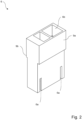
- Figure 3a shows a set of a printed circuit board 7 and a conductor connection module 1 according to the invention in a first embodiment with a contact insert according to the Figures 1a and 1b and an insulating housing 6 according to Figure 2 in a side view
- Figure 3b the corresponding set Figure 3a in a perspective view. It is clear that the solder connection contact surfaces 5a of the Contact element 5 can be soldered to the circuit board 7 through the openings 6a of the insulating housing 6.
- the insulating housing 6 has an insertion opening 6b for inserting an electrical conductor.
- the clamping point formed by the contact section 3c and the clamping leg 4a can be opened and/or closed via an actuating element 8, which in this case is designed as an actuating button, although other types of actuating elements 8 are also conceivable.
- a first recess 9a and a second recess 9b are arranged on the insulating housing 6.
- the recess 9a is designed as a type of overhang of the insulating housing 6, with the recess 9a overlapping the circuit board 7 in the assembled state.
- the circuit board 7 is thus arranged under the recess 9a and enables an improved fit of the conductor connection module 1.
- solder connection contact surfaces 7a of the circuit board 7 are present on the circuit board 7, wherein the solder connection contact surfaces 7a of the circuit board 7 can be soldered to solder connection contact surfaces 5a of a further conductor connection module 1.
- Figure 4a shows a set of a printed circuit board 7 and two conductor connection modules 1 according to the invention in a first embodiment in a side view, wherein Figure 4b shows the set according to Figure 4a in a perspective view.
- the set after the Figures 4a and 4b differs from the set according to the Figures 3a and 3b by having two conductor connection modules 1 instead of a single conductor connection module 1. It is clear that due to the symmetrical structure of the insulating housing 6, a conductor connection module 1 can be arranged on both opposite sides of the circuit board 7 and soldered to the circuit board 7 via the solder connection contact surfaces 5a. The insulating housing 6 can be positioned on one side of the circuit board 7 by means of the first recess 9a and the second recess 9b without having to structurally modify the insulating housing.
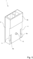
- Figure 5 shows a conductor connection module 1 in a second embodiment in a perspective view.
- the conductor connection module 1 according to Figure 5 differs from the embodiment according to Figure 3a to 4b in that a first recess 9a is arranged on the insulating housing 6, but no second recess.
- a locking element 10 is arranged on the side of the insulating housing on which the openings 6a are arranged, wherein the locking element is designed to lock with the circuit board 7.
- the locking element 10 can also be designed as a positioning element that enables better positioning on a circuit board.
- clearances 11 are arranged on the insulating housing 6 in the area of the openings 6a. This has the advantage that heat can be better supplied to the solder connection contact surface 6a in order to improve the soldering process to the circuit board 7.
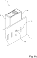
- Figure 6a shows a set of its circuit board 7 and a conductor connection module 1 in a second embodiment according to Figure 5 in a side view, where Figure 6b the set after Figure 6a in a perspective view.
- the locking element 10 is designed as a locking pin, wherein the locking element 10 engages in a corresponding locking recess 10a in the circuit board 7.
- the locking element 10 can ensure correct positioning of the conductor connection module 1 on the circuit board 7 and reduce the probability of incorrect positioning.
- the clearance 11 on the insulating housing 6 in the area of the solder connection contact surfaces protruding from the insulating housing 6 5a of the contact element 5, the solder connection contact surfaces 5a can be better soldered from the outside, since the heat supply can be carried out more easily.
- the clearance 11 is not designed to be so large that another electrical conductor could be inserted into the clearance 11. The probability of incorrect contact via the clearance 11 is to be avoided or reduced by the correspondingly small design of the clearance 11.
- Figure 7a shows a set of a printed circuit board 7 and two conductor connection modules 1 according to the invention in a second embodiment in a side view, wherein Figure 7b shows the set according to Figure 7a in a perspective view.
- the set after the Figures 7a and 7b differs from the set according to the Figures 6a and 6b by having two conductor connection modules 1 instead of a single conductor connection module 1.
- a conductor connection module 1 can be arranged on both sides of the circuit board 7 and soldered to the circuit board 7 via the solder connection contact surfaces 5a.
- the insulating housings 6 can be positioned on one side of the circuit board 7 using the respective first recess 9a.
- further installation space can be saved in this way.
- the conductor connection modules 1 are constructed in a mirror image so that the conductor connection modules continue to be symmetrical after assembly on the circuit board 7.
- Figure 8 shows a conductor connection module 1 in a third embodiment in a perspective view.
- two locking elements 10 are arranged on the conductor connection module 1, which are designed as locking pins.
- the different positioning of the locking elements 10 on the side of the insulating housing 6 on which the openings 6a are arranged ensures exact positioning of the conductor connection module 1 on a circuit board 7 provided for it with corresponding locking recesses 10a. Incorrect positioning is reduced or avoided by the position of the locking elements 10.
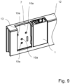
- Figure 9 shows a set of a circuit board 7 arranged in a housing 12 and a conductor connection module 1 according to Figure 8 in a perspective view.
- the circuit board 7 is arranged in a housing 12, wherein conductor connection modules 1 can be inserted into a corresponding recess 13 of the housing 12.
- the conductor connection modules 1 can be better placed on the circuit board 7, wherein the circuit board 7 and at least some of the conductor connection modules 1 are protected from external influences by the housing 12.
- the housing 12 is a housing 12 of an electronic device, which can also be snapped onto a mounting rail, for example.
- corresponding locking recesses 10a are provided on the circuit board 7 so that the corresponding conductor connection modules 1 can be positioned in the correct position on the circuit board 7.
- corresponding conductor connection modules 1 can only be positioned on one side of the circuit board 7.
- conductor connection modules 1 can be positioned on both sides of the circuit board 7.
- the housing 12 then has corresponding recesses 13 on both sides of the circuit board 7.
- Figure 10 shows a set of a circuit board 7 arranged in a housing 12 and a plurality of conductor connection modules 1 according to Figure 8 in a perspective view.
- Corresponding conductor connection modules 1 can be soldered onto opposite sides of the circuit board 7.
- the locking pins 10 of the conductor connection module 1 engage in the locking recesses 10a provided for this purpose in order to ensure the correct positioning of the conductor connection module 1.
- recesses 13 opposite one another are also arranged on the housing 12 in order to position the corresponding conductor connection modules 1 on the circuit board 7.
- Figure 11 shows a conductor connection module 1 in a fourth embodiment in a perspective view.
- the conductor connection module 1 has an additional corresponding recess 14.
- a dome which is arranged, for example, on a housing 13 or directly on a circuit board 7, can engage in the corresponding recess 14. This connection can further fix the conductor connection module 1 in position on the circuit board 7.
- the dome can be caulked after assembly so that non-destructive separation of the components is no longer possible.
- an additional metal part in particular for example a metal pin, can be inserted into the recess 14, which can be soldered to the circuit board and can serve as an additional fastening of the terminal on the circuit board.
- Figure 12a shows a conductor connection module 1 in a fifth embodiment in a perspective view.
- the conductor connection module 1 only has a larger opening 6a in the insulating housing 6 through which two solder connection contact surfaces 5a of the contact elements 5 protrude.
- the solder connection contact surfaces 5a are not designed as front sides of the contact elements 5, but are provided by bending the contact elements 5. In this way, a larger surface of the solder connection contact surfaces 5a can be provided in order to enlarge the soldering surface on a circuit board 7.
- a test opening 18 is arranged on the conductor connection module 1 in the embodiment shown.
- Figure 12b shows a conductor connection module 1 in a sixth embodiment in a perspective view.
- this conductor connection module 1 is additionally extended by a slot 15.
- This slot 15 can, for example, be wider than the insertion opening 6b for the electrical conductor.
- the slot 15 can be assigned an associated slot contact 15a, which can be soldered to a corresponding circuit board.
- Figure 13 shows a contact insert 2 for a conductor connection module 1 according to the Figures 12a and 12b in a perspective view in a second embodiment.
- solder connection contact surfaces 5a of the contact elements 5 are provided in that the contact elements 5 are each bent at their free ends and thus provide a surface for soldering to a circuit board 7.
- solder connection contact surfaces 5a are essentially arranged on a common imaginary straight line and/or plane.
- solder connection contact surfaces 5a are arranged on the side of the busbar 3 facing away from the clamping point, i.e. on the rear side 16 of the connecting section 3b.
- Figure 14 shows a circuit board 7 with a contact insert 2 after Figure 13 in a perspective view.
- Figure 14 is intended in particular to illustrate the assembly of a conductor connection module 1 according to the invention on the circuit board 7, with the insulating housing 6 being hidden for improved clarity.
- the conductor connection module is soldered to the solder connection contact surfaces 5a of the contact elements 5 of the contact insert 2 on the circuit board 7.
- the solder connection contact surface 5a of the slot 15 for a bridging plug, for example was soldered to the circuit board 7.
- Figure 15 shows a set of a circuit board 7 arranged in a housing 12 according to the Figure 14 and a conductor connection module according to Figures 12a and 12b in a perspective view, wherein in this embodiment two housings 12, each with a circuit board 7, are arranged behind or next to each other.
- a bridging plug 17 is arranged in the slots 15 provided for this purpose.
- the bridging plug 17 can be used to achieve an electrically conductive connection between the circuit boards 7, which are accommodated in respective housings 12 arranged next to or behind one another.
- Figure 16a shows a conductor connection module 1 in a seventh embodiment in a perspective view. It can be seen that two locking elements 10 are arranged on the conductor connection module 1, which can be inserted into a corresponding locking recess 10a of a circuit board 7.
- the locking elements 10 can be dimensioned to different sizes. In this way, incorrect positioning of the conductor connection module 1 on the circuit board 7 can be further reduced.
- locking lugs 19 are arranged in the housing, wherein the contact insert 2 can be locked with the locking lugs 19 in order to ensure that the contact insert is securely seated.
- the conductor connection module 1 has only a larger opening 6a in the insulating housing 6 through which two solder connection contact surfaces 5a of the contact elements 5 protrude. It is clear that the solder connection contact surfaces 5a are not designed as front sides of the contact elements 5. The exact design of the contact element 5 is described below under the Figure 17 explained in more detail.
- Figure 16b shows a conductor connection module 1 in an eighth embodiment in a perspective view.
- This conductor connection module 1 is additionally extended by a slot 15.
- This slot 15 can, for example, be wider than the insertion opening 6b for the electrical conductor.
- a bridging plug for the electrically conductive connection of two conductor connection modules 1 can then be inserted into such a slot 15.
- the slot 15 can be soldered to a circuit board 7 in an electrically conductive manner via a corresponding solder connection contact surface 5a.
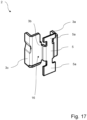
- Figure 17 shows a contact insert 2 for a conductor connection module 1 according to the Figures 16a and 16b in a perspective view in a third embodiment. It is clear that the contact element 5 is protruding from the connecting section 3b of the busbar 3. The connecting section 3b thus simultaneously forms the contact element 5.
- the solder connection contact surfaces 5a are arranged on the side of the busbar 3 facing away from the clamping point, i.e. on the rear side 16 of the connecting section 3b.
- Figure 18 shows a set of a printed circuit board 7 and conductor connection modules 1 according to the Figures 16a and 16b in a perspective view. It is clear that the conductor connection modules 1 are inserted into the corresponding recesses 10a via the locking elements 10 in order to ensure the correct positioning of the conductor connection modules 1.
- Figure 19 shows a set of a circuit board 7 arranged in a housing 12 according to the Figure 18 and conductor connection modules 1 according to Figures 16a and 16b in a perspective view. It is clear that a bridging plug 17 is arranged in the slots 15 provided for it. The bridging plug 17 can be used to create an electrically conductive connection between the corresponding conductor connection modules 1.
- Figure 20 shows a contact insert 2 for a conductor connection module 1 in a further embodiment.
- an offset is arranged on the connecting section 3b of the busbar 3.
- the offset is achieved by bends 20 in the connecting section 3b.
- the offset can only be achieved via a single bend 20.
- the busbar 3 is formed in one piece in this embodiment.
- solder connection contact surfaces 5a are thus positioned out of the plane of the connecting section 3b.
- the solder connection contact surfaces 3a are thus arranged on the side of the busbar 3 facing away from the terminal points.
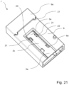
- Figure 21 shows a conductor connection module 1 with a contact insert according to Figure 20 in a further embodiment.
- the solder connection contact surfaces 5a of the busbar 3 can protrude from the opening 6a of the insulating housing 6 due to the offset.
- the stability of the contact insert 2 is improved by the offset.
- lugs 21 can be seen on the insulating housing 6 in the area of the first recess 9a.
- the locking lugs 21 allow the conductor connection module 1 to be hooked into correspondingly provided contours on a circuit board, which further improves the positioning of the conductor connection module 1 on the circuit board.
- the conductor connection module 1 can be secured in the insulating housing 6 in a form-fitting manner.
- at least one locking lug 21 of the insulating housing 6 can be present, which projects into the opening 6a and forms a stop together with a cutout 22 of the contact insert 2.
- the locking lug 21 can extend from the bottom of the insulating housing 6 to the open outside of the opening 6a and form a stop with an edge 23 of the solder connection contact surface 5a.
- the locking lug 21 projects laterally into a side wall surface of the contact insert 2, for example in the width direction of the contact insert 2.
- This side wall surface can be a wall surface of the bend 20 that is transverse to the solder connection surface 5a.
- Other design solutions for a corresponding locking of the contact insert 2 on the insulating housing 6 are conceivable.
Landscapes
- Coupling Device And Connection With Printed Circuit (AREA)
- Multi-Conductor Connections (AREA)
Abstract
Description
- Die Erfindung betrifft ein Leiteranschlussmodul mit einem Isolierstoffgehäuse und einem in dem Isolierstoffgehäuse angeordneten Kontakteinsatz, wobei der Kontakteinsatz eine Stromschiene und eine Klemmfeder hat, wobei an der Stromschiene wenigstens ein Kontaktelement mit einer Lötanschlusskontaktfläche angeordnet ist, wobei die Lötanschlusskontaktfläche an einer Leiterplatte anlötbar ist.
- Ausgehend hiervon ist es Aufgabe der vorliegenden Erfindung, ein verbessertes Leiteranschlussmodul zu schaffen.
- Die Aufgabe wird mit einem Leiteranschlussmodul mit den Merkmalen des Anspruchs 1 gelöst. Weiterhin wird die Aufgabe mit einem Set aus Leiteranschlussmodul und einer Leiterplatte mit den Merkmalen des Anspruchs 15 gelöst. Vorteilhafte Ausführungsformen sind in den Unteransprüchen beschrieben.
- Bei dem gattungsgemäßen Leiteranschlussmodul wird vorgeschlagen, dass die Stromschiene als rahmenförmige Stromschiene ausgebildet ist, wobei die rahmenförmige Stromschiene einen Kontaktabschnitt und einen Halteabschnitt hat, die einander gegenüberliegend ausgebildet sind und wobei der Kontaktabschnitt und der Halteabschnitt über einen Verbindungsabschnitt miteinander verbunden sind, wobei die Klemmfeder einen Anlageschenkel zur Anlage an dem Halteabschnitt und einen Klemmschenkel hat, wobei der Klemmschenkel und der Kontaktabschnitt eine Klemmstelle für einen anzuklemmenden elektrischen Leiter bilden, wobei wenigstens ein Kontaktelement am Halteabschnitt und/oder am Kontaktabschnitt angeordnet ist und die Lötanschlusskontaktfläche des Kontaktelementes aus einer Öffnung des Isolierstoffgehäuses herausragt.
- Dies hat den Vorteil, dass ein kompaktes Leiteranschlussmodul bereitgestellt werden kann, das über die Lötanschlusskontaktflächen an eine Leiterplatte anlötbar ist, ohne das Isolierstoffgehäuse zu entfernen.
- Es kann jeweils ein Kontaktelement am Halteabschnitt und am Kontaktabschnitt angeordnet sein und aus jeweils einer Öffnung aus dem Isolierstoffgehäuse herausragen. Auf diese Weise kann die elektrisch leitende Kontaktierung des Leiteranschlussmoduls an eine Leiterplatte weiter verbessert werden. Ferner vorteilhaft können die Lötanschlusskontaktflächen der Kontaktelemente parallel zueinander ausgerichtet sein
- Das Kontaktelement kann sich in Verlängerung des Halteabschnittes und/oder des Kontaktabschnittes aus der Öffnung des Isolierstoffgehäuses erstrecken. Auf diese Weise können auf einfache konstruktive Art entsprechende Kontaktabschnitte bereitgestellt werden.
- Es ist denkbar, dass der Halteabschnitt und/oder der Kontaktabschnitt und die Kontaktelemente dabei einstückig ausgebildet sein können. Das Kontaktelement erstreckt sich dann vorteilhaft in derselben Ebene, die durch den jeweiligen Halteabschnitt und/oder Kontaktabschnitt aufgespannt wird.
- Alternativ wäre bei einer einteiligen Ausführung auch ein Versatz zwischen dem Halte-/Kontaktabschnitt und dem Kontaktelement denkbar.
- Eine Stirnseite des Kontaktelementes kann als Lötanschlusskontaktfläche ausgebildet sein.
- Die Dicke des Kontaktelementes entspricht dabei der Breite der Lötanschlusskontaktflächen. Die Länge der Lötanschlusskontaktflächen entspricht dabei im Wesentlichen der Länge des vom Halteabschnitt und/oder Kontaktabschnitts abragenden Kontaktelements.
- Die Lötanschlusskontaktfläche des Kontaktelementes kann für eine SMD-Lötung auf die Leiterplatte eine im Wesentlichen ebene Kontaktoberfläche haben.
- Die Stromschiene kann U-förmig ausgebildet sein. Eine U-förmige Ausbildung kann auch ähnliche Formen, wie zum Beispiel eine V-förmige oder C-förmige Ausbildung, umfassen. Die Stromschiene kann einen Klemmkäfig bilden, in dem die Klemmfeder eingespannt ist.
- Der Klemmschenkel der Klemmfeder kann in einen Federbogen übergehen, wobei sich der Federbogen in den Anlageschenkel zur Anlage an dem Halteabschnitt der Stromschiene erstreckt, wobei die Klemmfeder V-förmig ausgebildet ist.
- Das Isolierstoffgehäuse kann an der Seite des Isolierstoffgehäuses, an der die Öffnung angeordnet ist, einen ersten Rücksprung haben, wobei die Leiterplatte an dem ersten Rücksprung anordbar ist.
- Ein Rücksprung kann insbesondere ein Überhang des Isolierstoffgehäuses sein, sodass die Leiterplatte unter dem Überhang angeordnet und mit den Lötanschlusskontaktflächen verbunden werden kann. Der Überhang ummantelt oder umgreift die Leiterplatte somit zumindest zum Teil. Durch einen Rücksprung kann eine Abstufung des Isolierstoffgehäuses ausgebildet sein, so dass eine Gehäusewand des Isolierstoffgehäuses auf einer Seite des Rücksprungs mit einem Versatz auf einem anderen Niveau verläuft als auf der anderen Seite des Rücksprungs. Dabei können die Abschnitte der Gehäusewand auf den beiden Seiten des Rücksprungs parallel zueinander verlaufen. Der Versatz kann z.B. eine Abmessung haben, die im Wesentlichen der Hälfte der Dicke einer Leiterplatte entspricht.
- Das Isolierstoffgehäuse kann an der der Öffnung gegenüberliegenden Seite einen zweiten Rücksprung haben, wobei die Leiterplatte an dem zweiten Rücksprung anordbar ist.
- Insbesondere ist denkbar, dass an dem Leiteranschlussmodul ein erster Rücksprung und ein zweiter Rücksprung angeordnet sein können. Dies hat den Vorteil, dass dieselbe Art von Leiteranschlussmodul an einander gegenüberliegenden Seiten einer einzelnen Leiterplatte angeordnet werden kann, ohne die Variantenanzahl erhöhen zu müssen.
- Das Isolierstoffgehäuse kann an der Seite des Isolierstoffgehäuses, an der die Öffnung angeordnet ist, wenigstens ein Rastelement zur Verrastung mit der Leiterplatte haben. Ferner vorteilhaft kann das Rastelement als Rastzapfen ausgebildet sein, wobei der Rastzapfen in eine korrespondierende Rastausnehmung der Leiterplatte einführbar ist.
- Es hat sich gezeigt, dass insbesondere eine Vielzahl von Rastzapfen, insbesondere zwei Rastzapfen geeignet sind, eine definierte Positionierung des Leiteranschlussmodules auf der Leiterplatte zu ermöglichen, da die Rastzapfen nur in die dafür vorgesehenen korrespondierenden Rastausnehmungen eingeführt werden können. Somit ist die Wahrscheinlichkeit einer falschen Positionierung oder einer Verdrehung des Leiteranschlussmoduls gegenüber der Leiterplatte verringert.
- Das Rastelement kann verschieblich in dem Isolierstoffgehäuse gelagert sein.
- Dabei ist sowohl eine vertikale Verschiebung (in Haupterstreckungsrichtung des Leiteranschlussmoduls), als auch eine horizontale Verschiebung (quer zur Haupterstreckungsrichtung des Leiteranschlussmoduls) denkbar.
- Im Bereich der Lötanschlusskontaktflächen des Kontaktelementes kann eine Freimachung am Isolierstoffgehäuse angeordnet sein.
- Die Freimachung hat den Vorteil, dass insbesondere Wärme der Lötanschlusskontaktfläche besser zugeführt werden kann, um den Anlötvorgang an die Leiterplatte zu verbessern. Die Freimachung hat insbesondere nicht den Zweck, weitere Leiter mit dem Leiteranschlussmodul und/oder der Leiterplatte zu verbinden. Die Freimachung ist deswegen insbesondere nicht derartig groß, dass ein elektrischer Leiter in die Freimachung auf einfache Weise eingesteckt werden kann, sodass eine Fehlkontaktierung ausgelöst wird
- Ferner wird die Aufgabe gelöst durch ein Set aus einer Leiterplatte und einem oben beschriebenen Leiteranschlussmodul Leiteranschlussmodul.
- Die Leiterplatte kann in einem Gehäuse angeordnet sein, wobei das Leiteranschlussmodul in eine Aussparung des Gehäuses einsetzbar ist.
- Auf diese Weise können die Leiteranschlussmodule besser an der Leiterplatte platziert werden, wobei die Leiterplatte und zumindest ein Teil der Leiteranschlussmodule durch das Gehäuse vor äußeren Einflüssen geschützt werden. Es ist denkbar, dass das Gehäuse ein Gehäuse eines elektronischen Gerätes ist, das zum Beispiel auch auf einer Tragschiene aufrastbar sein kann.
- Aufeinander gegenüberliegenden Seiten der Leiterplatte kann mindestens ein Leiteranschlussmodul angeordnet sein. Auf diese Weise kann der Raum zur Positionierung von mehreren Leiteranschlussmodulen an der Leiterplatte effizient ausgenutzt werden.
- An dem Gehäuse kann ein Dom angeordnet sein, wobei der Dom in eine korrespondierende erste Ausnehmung in der Leiterplatte und eine korrespondierende zweite Ausnehmung im Isolierstoffgehäuse des Leiteranschlussmodules steckbar ist.
- Der Dom kann insbesondere nach Einführung in die korrespondierende Ausnehmung verstemmt werden. Auf diese Weise kann die Leiterplatte und das Leiteranschlussmodul nicht mehr zerstörungsfrei voneinander getrennt werden.
- Der unbestimmte Begriff "ein" ist als solcher und nicht als Zahlwort zu verstehen. So ist zum Beispiel auch denkbar, dass eine Vielzahl von Lötanschlusskontaktflächen, zum Beispiel zwei, drei oder vier, an einem Kontaktelement oder mehreren Kontaktelementen vorhanden sind.
- Die Erfindung wird nachfolgend anhand von Ausführungsbeispielen beispielhaft mit den beigefügten Zeichnungen näher erläutert. Es zeigen:
- Figur 1a -
- zeigt einen Kontakteinsatz in einer ersten Ausführungsform für ein erfindungsgemäßes Leiteranschlussmodul in einer perspektivischen Ansicht;
- Figur 1b -
- zeigt einen Kontakteinsatz nach
Figur 1a in einer Seitenansicht; - Figur 2 -
- zeigt ein Isolierstoffgehäuse für ein erfindungsgemäßes Leiteranschlussmodul in einer perspektivischen Ansicht;
- Figur 3a -
- zeigt ein Set aus einer Leiterplatte und einem erfindungsgemäßen Leiteranschlussmodul in einer ersten Ausführungsform in einer Seitenansicht
- Figur 3b -
- zeigt ein Set nach
Figur 3a in einer perspektivischen Ansicht; - Figur 4a -
- zeigt ein Set aus einer Leiterplatte und zwei erfindungsgemäßen Leiteranschlussmodulen in einer ersten Ausführungsform in einer Seitenansicht;
- Figur 4b -
- zeigt ein Set nach
Figur 4a in einer perspektivischen Ansicht; - Figur 5 -
- zeigt ein Leiteranschlussmodul in einer zweiten Ausführungsform in einer perspektivischen Ansicht;
- Figur 6a -
- zeigt ein Set aus seiner Leiterplatte und einem Leiteranschlussmodul in einer zweiten Ausführungsform nach
Figur 5 in einer Seitenansicht; - Figur 6b -
- zeigt ein Set nach
Figur 6a in einer perspektivischen Ansicht; - Figur 7a -
- zeigt ein Set aus einer Leiterplatte und zwei Leiteranschlussmodulen in einer zweiten Ausführungsform in einer Seitenansicht;
- Figur 7b -
- zeigt ein Set nach
Figur 7a in einer perspektivischen Ansicht; - Figur 8 -
- zeigt ein Leiteranschlussmodul in einer dritten Ausführungsform in einer perspektivischen Ansicht;
- Figur 9 -
- zeigt ein Set aus einer in einem Gehäuse angeordneten Leiterplatte und eines Leiteranschlussmoduls nach
Figur 8 in einer perspektivischen Ansicht; - Figur 10 -
- zeigt ein Set aus einer in einem Gehäuse angeordneten Leiterplatte und einer Mehrzahl von Leiteranschlussmoduls nach
Figur 8 in einer perspektivischen Ansicht; - Figur 11 -
- zeigt ein Leiteranschlussmodul in einer vierten Ausführungsform in einer perspektivischen Ansicht;
- Figur 12a -
- zeigt ein Leiteranschlussmodul in einer fünften Ausführungsform in einer perspektivischen Ansicht;
- Figur 12b -
- zeigt ein Leiteranschlussmodul in einer sechsten Ausführungsform in einer perspektivischen Ansicht;
- Figur 13 -
- zeigt einen Kontakteinsatz für ein Leiteranschlussmodul nach den Figuren 12a und 12b in einer perspektivischen Ansicht;
- Figur 14 -
- zeigt eine Leiterplatte mit einem Kontakteinsatz nach der
Figur 13 in einer perspektivischen Ansicht; - Figur 15 -
- zeigt ein Set aus einer in einem Gehäuse angeordneten Leiterplatte nach der
Figur 14 und eines Leiteranschlussmoduls nach denFiguren 12a und12b in einer perspektivischen Ansicht; - Figur 16a -
- zeigt ein Leiteranschlussmodul in einer siebten Ausführungsform in einer perspektivischen Ansicht;
- Figur 16b -
- zeigt ein Leiteranschlussmodul in einer achten Ausführungsform in einer perspektivischen Ansicht;
- Figur 17 -
- zeigt einen Kontakteinsatz für ein Leiteranschlussmodul nach den Figuren 16a und 16b in einer perspektivischen Ansicht;
- Figur 18 -
- zeigt ein Set aus einer Leiterplatte und Leiteranschlussmodulen nach den
Figuren 16a und16b in einer perspektivischen Ansicht; - Figur 19 -
- zeigt ein Set aus einer in einem Gehäuse angeordneten Leiterplatte nach der
Figur 18 und von Leiteranschlussmodulen nach denFiguren 16a und16b in einer perspektivischen Ansicht, - Figur 20 -
- zeigt ein Leiteranschlussmodul für einen Kontakteinsatz in einer weiteren Ausführungsform,
- Figur 21 -
- zeigt ein Leiteranschlussmodul mit einem Kontakteinsatz nach
Figur 20 in einer weiteren Ausführungsform. -
Figur 1a zeigt einen Kontakteinsatz 2 in einer ersten Ausführungsform für ein erfindungsgemäßes Leiteranschlussmodul 1 in einer perspektivischen Ansicht, wobei Figur 1b den Kontakteinsatz 2 nachFigur 1a in einer Seitenansicht zeigt. Der Kontakteinsatz hat eine Stromschiene 3 und eine Klemmfeder 4. Die Stromschiene 3 ist dabei als rahmenförmige Stromschiene 3 ausgebildet. Die rahmenförmige Stromschiene 3 ist dabei im Wesentlichen U-förmig ausgebildet. Die Stromschiene 3 hat dabei einen Halteabschnitt 3a und einen Kontaktabschnitt 3c, wobei der Halteabschnitt 3a und der Kontaktabschnitt 3c über einen Verbindungsabschnitt 3b miteinander verbunden sind. Der Halteabschnitt 3a und der Kontaktabschnitt 3c sind einander gegenüberliegend ausgebildet. - Die Klemmfeder 4 hat einen Klemmschenkel 4a, wobei der Klemmschenkel 4a in einen Federbogen 4b übergeht und wobei der Federbogen 4b in einen Anlageschenkel 4c übergeht und der Anlageschenkel 4c zur Anlage an dem Halteabschnitt 3a der Stromschiene 3 ausgebildet ist. Die Klemmfeder 4 ist im Wesentlichen V-förmig ausgebildet. Der Kontaktabschnitt 3c und der Klemmschenkel 4a der Klemmfeder 4 bilden dabei eine Klemmstelle für einen anzuklemmenden elektrischen Leiter.
- Sowohl an dem Halteabschnitt 3a, als auch an dem Kontaktabschnitt 3b ist jeweils ein Kontaktelement 5 angeordnet. Das Kontaktelement 5 erstreckt sich dabei in diesem Ausführungsbeispiel in Verlängerung des jeweiligen Halteabschnittes 3a und des jeweiligen Kontaktabschnittes 3b. Die Stirnseiten der Kontaktelemente 5 sind dabei als Lötanschlusskontaktflächen 5a ausgebildet. Die Lötanschlusskontaktflächen 5a haben dabei eine im Wesentlichen ebene Oberfläche und können an eine entsprechende Leiterplatte, zum Beispiel über ein SMD-Lötverfahren, angelötet werden.
-
Figur 2 zeigt ein Isolierstoffgehäuse 6 für ein erfindungsgemäßes Leiteranschlussmodul 1 in einer perspektivischen Ansicht. Das Isolierstoffgehäuse 6 hat dabei einen länglichen und/oder quaderförmigen Grundkörper, in den ein Kontakteinsatz, zum Beispiel ein Kontakteinsatz nach denFiguren 1a und1b , eingesetzt werden kann. Das Isolierstoffgehäuse 6 hat zwei Öffnungen 6a, wobei durch die Öffnungen 6a die Lötanschlusskontaktflächen 5a des Kontaktelementes 5 herausragen können. -
Figur 3a zeigt ein Set aus einer Leiterplatte 7 und einem erfindungsgemäßen Leiteranschlussmodul 1 in einer ersten Ausführungsform mit einem Kontakteinsatz nach denFiguren 1a und1b und einem Isolierstoffgehäuse 6 nachFigur 2 in einer Seitenansicht, wohingegenFigur 3b das entsprechende Set nachFigur 3a in einer perspektivischen Ansicht zeigt. Deutlich wird, dass die Lötanschlusskontaktflächen 5a des Kontaktelementes 5 durch die Öffnungen 6a des Isolierstoffgehäuses 6 an der Leiterplatte 7 anlötbar sind. - Insbesondere die Zusammenschau der
Figuren 1 bis 3b verdeutlicht den Kern der vorliegenden Erfindung. Es wird deutlich, dass das Isolierstoffgehäuse 6 eine Einführungsöffnung 6b zum Einführen eines elektrischen Leiters hat. Über einen Betätigungselement 8, das in diesem Fall als Betätigungsdrücker ausgebildet ist, wobei auch andere Arten von Betätigungselementen 8 denkbar sind, kann die durch den Kontaktabschnitt 3c und dem Klemmschenkel 4a gebildete Klemmstelle geöffnet und/oder geschlossen werden. - Weiterhin zu erkennen ist, dass an dem Isolierstoffgehäuse 6 ein erster Rücksprung 9a und ein zweiter Rücksprung 9b angeordnet ist. Der Rücksprung 9a ist dabei als eine Art Überhang des Isolierstoffgehäuses 6 ausgebildet, wobei der Rücksprung 9a die Leiterplatte 7 im montierten Zustand übergreift. Die Leiterplatte 7 ist somit unter dem Rücksprung 9a angeordnet und ermöglicht einen verbesserten Sitz des Leiteranschlussmoduls 1.
- Aus der
Figur 3a wird deutlich, dass an der Leiterplatte 7 entsprechende Lötanschlusskontaktflächen 7a der Leiterplatte 7 vorhanden sind, wobei die Lötanschlusskontaktflächen 7a der Leiterplatte 7 mit Lötanschlusskontaktflächen 5a eines weiteren Leiteranschlussmoduls 1 verlötet werden können. -
Figur 4a zeigt ein Set aus einer Leiterplatte 7 und zwei erfindungsgemäßen Leiteranschlussmodulen 1 in einer ersten Ausführungsform in einer Seitenansicht, wobei Figur 4b das Set nachFigur 4a in einer perspektivischen Ansicht zeigt. - Das Set nach den
Figuren 4a und4b unterscheidet sich von dem Set nach denFiguren 3a und3b dadurch, dass zwei Leiteranschlussmodule 1 anstatt eines einzelnen Leiteranschlussmoduls 1 vorhanden sind. Deutlich wird, dass durch den symmetrischen Aufbau des Isolierstoffgehäuses 6 an beiden einander gegenüberliegenden Seiten der Leiterplatte 7 jeweils ein Leiteranschlussmodul 1 angeordnet und über die Lötanschlusskontaktflächen 5a mit der Leiterplatte 7 verlötet werden kann. Dabei kann durch den ersten Rücksprung 9a und den zweiten Rücksprung 9b das Isolierstoffgehäuse 6 auf jeweils einer Seite der Leiterplatte 7 positioniert werden, ohne dabei das Isolierstoffgehäuse baulich verändern zu müssen. -
Figur 5 zeigt ein Leiteranschlussmodul 1 in einer zweiten Ausführungsform in einer perspektivischen Ansicht. Das Leiteranschlussmodul 1 nachFigur 5 unterscheidet sich von der Ausführungsform nachFigur 3a bis 4b dadurch, dass an dem Isolierstoffgehäuse 6 ein erster Rücksprung 9a angeordnet ist, aber kein zweiter Rücksprung. - Deutlich wird, dass an der Seite des Isolierstoffgehäuses, an der die Öffnungen 6a angeordnet sind, ein Rastelement 10 angeordnet ist, wobei das Rastelement zur Verrastung mit der Leiterplatte 7 ausgebildet ist. Das Rastelement 10 kann auch als Positionierelement ausgebildet sein, das eine bessere Positionierung an einer Leiterplatte ermöglicht.
- Weiterhin wird deutlich, dass an dem Isolierstoffgehäuse 6 in dem Bereich der Öffnungen 6a Freimachungen 11 angeordnet sind. Dies hat den Vorteil, dass Wärme der Lötanschlusskontaktfläche 6a besser zugeführt werden kann, um den Anlötvorgang an die Leiterplatte 7 zu verbessern.
-
Figur 6a zeigt ein Set aus seiner Leiterplatte 7 und einem Leiteranschlussmodul 1 in einer zweiten Ausführungsform nachFigur 5 in einer Seitenansicht, wobeiFigur 6b das Set nachFigur 6a in einer perspektivischen Ansicht zeigt. - Deutlich wird, dass das Rastelement 10 als Rastzapfen ausgebildet ist, wobei das Rastelement 10 in eine korrespondierende Rastausnehmung 10a in der Leiterplatte 7 eingreift. Durch das Rastelement 10 kann dabei eine korrekte Positionierung des Leiteranschlussmoduls 1 an der Leiterplatte 7 sichergestellt und die Wahrscheinlichkeit einer falschen Positionierung verringert werden.
- Deutlich wird weiterhin, dass durch die Freimachung 11 am Isolierstoffgehäuse 6 im Bereich der aus dem Isolierstoffgehäuse 6 herausragenden Lötanschlusskontaktflächen 5a des Kontaktelementes 5, die Lötanschlusskontaktflächen 5a von außen besser verlötet werden können, da die Wärmezufuhr einfacher erfolgen kann. Die Freimachung 11 ist dabei aber nicht derartig groß ausgebildet, dass ein weiterer elektrischer Leiter in die Freimachung 11 eingesteckt werden könnte. Die Wahrscheinlichkeit einer Fehlkontaktierung über die Freimachung 11 soll durch die entsprechend kleine Ausbildung der Freimachung 11 vermieden bzw. verringert werden.
-
Figur 7a zeigt ein Set aus einer Leiterplatte 7 und zwei erfindungsgemäßen Leiteranschlussmodulen 1 in einer zweiten Ausführungsform in einer Seitenansicht, wobei Figur 7b das Set nachFigur 7a in einer perspektivischen Ansicht zeigt. - Das Set nach den
Figuren 7a und7b unterscheidet sich von dem Set nach denFiguren 6a und6b dadurch, dass zwei Leiteranschlussmodule 1 anstatt ein einzelnes Leiteranschlussmodul 1 vorhanden sind. - Deutlich wird, dass an beiden Seiten der Leiterplatte 7 jeweils ein Leiteranschlussmodul 1 angeordnet und über die Lötanschlusskontaktflächen 5a mit der Leiterplatte 7 verlötet werden können. Dabei können die Isolierstoffgehäuse 6 durch den jeweiligen ersten Rücksprung 9a auf jeweils einer Seite der Leiterplatte 7 positioniert werden. Im Unterschied zu einem Leiteranschlussmodul 1 mit einem zweiten Rücksprung kann auf diese Weise weiter Bauraum eingespart werden. Die Leiteranschlussmodule 1 sind im Gegensatz zu den Leiteranschlussmodulen 1 nach den Figuren 4a und 4b spiegelverkehrt aufgebaut, damit nach der Montage an der Leiterplatte 7 weiterhin eine Symmetrie der Leiteranschlussmodule vorhanden ist.
-
Figur 8 zeigt ein Leiteranschlussmodul 1 in einer dritten Ausführungsform in einer perspektivischen Ansicht. Im Unterschied zur zweiten Ausführungsform nachFigur 5 wird deutlich, dass an dem Leiteranschlussmodul 1 zwei Rastelemente 10 angeordnet sind, die als Rastzapfen ausgebildet sind. Die unterschiedliche Positionierung der Rastelemente 10 an der Seite des Isolierstoffgehäuses 6, an dem die Öffnungen 6a angeordnet sind, gewährleistet eine exakte Positionierung des Leiteranschlussmodules 1 an einer dafür vorgesehenen Leiterplatte 7 mit entsprechenden Rastausnehmungen 10a. Eine Fehlpositionierung wird durch die Lage der Rastelemente 10 verringert bzw. vermieden. -
Figur 9 zeigt ein Set aus einer in einem Gehäuse 12 angeordneten Leiterplatte 7 und eines Leiteranschlussmoduls 1 nachFigur 8 in einer perspektivischen Ansicht. Zu erkennen ist, dass die Leiterplatte 7 in einem Gehäuse 12 angeordnet ist, wobei Leiteranschlussmodule 1 in eine entsprechende Aussparung 13 des Gehäuses 12 eingesetzt werden können. Auf diese Weise können die Leiteranschlussmodule 1 besser an der Leiterplatte 7 platziert werden, wobei die Leiterplatte 7 und zumindest ein Teil der Leiteranschlussmodule 1 durch das Gehäuse 12 vor äußeren Einflüssen geschützt werden. Es ist denkbar, dass das Gehäuse 12 ein Gehäuse 12 eines elektronischen Gerätes ist, das zum Beispiel auch auf einer Tragschiene aufrastbar sein kann. - Deutlich wird weiterhin, dass an der Leiterplatte 7 korrespondierende Rastausnehmungen 10a vorgesehen sind, damit die entsprechenden Leiteranschlussmodule 1 an der korrekten Position an der Leiterplatte 7 positioniert werden können. In diesem Ausführungsbeispiel können nur auf einer Seite der Leiterplatte 7 entsprechende Leiteranschlussmodule 1 positioniert werden. Es ist aber auch denkbar, dass auf beiden Seiten der Leiterplatte 7 Leiteranschlussmodule 1 positioniert werden können. Das Gehäuse 12 weist dann entsprechende Aussparungen 13 auf beiden Seiten der Leiterplatte 7 auf.
-
Figur 10 zeigt ein Set aus einer in einem Gehäuse 12 angeordneten Leiterplatte 7 und einer Mehrzahl von Leiteranschlussmodulen 1 nachFigur 8 in einer perspektivischen Ansicht. Im Unterschied zuFigur 9 können an gegenüberliegenden Seiten der Leiterplatte 7 entsprechende Leiteranschlussmodule 1 angelötet werden. Dabei greifen die Rastzapfen 10 des Leiteranschlussmodules 1 in die dafür vorgesehenen Rastausnehmungen 10a ein, um die korrekte Positionierung des Leiteranschlussmodules 1 zu gewährleisten. Weiterhin sind am Gehäuse 12 auch einander gegenüberliegende Aussparungen 13 angeordnet, um die entsprechenden Leiteranschlussmodule 1 an der Leiterplatte 7 zu positionieren. -
Figur 11 zeigt ein Leiteranschlussmodul 1 in einer vierten Ausführungsform in einer perspektivischen Ansicht. Im Unterschied zum Leiteranschlussmodul 1 in der dritten Ausführungsform nachFigur 8 , hat das Leiteranschlussmodul 1 eine zusätzliche korrespondierende Ausnehmung 14. Dabei kann ein Dom, der zum Beispiel an einem Gehäuse 13 oder direkt an einer Leiterplatte 7 angeordnet ist, in die korrespondierende Ausnehmung 14 eingreifen. Diese Verbindung kann das Leiteranschlussmodul 1 weiter in der Position an der Leiterplatte 7 fixieren. Zusätzlich kann der Dom nach der Montage verstemmt werden, sodass eine zerstörungsfreie Trennung der Bauteile nicht mehr möglich ist. - Es ist denkbar, dass in die Ausnehmung 14 ein zusätzliches Metallteil, insbesondere zum Beispiel ein Metallstift, eingesteckt werden kann, das mit der Leiterplatte verlötet werden und als zusätzliche Befestigung der Klemme auf der Leiterplatte dienen kann.
-
Figur 12a zeigt ein Leiteranschlussmodul 1 in einer fünften Ausführungsform in einer perspektivischen Ansicht. Im Unterschied zu der ersten bis vierten Ausführungsform hat das Leiteranschlussmodul 1 lediglich eine größere Öffnung 6a im Isolierstoffgehäuse 6 durch die, zwei Lötanschlusskontaktflächen 5a der Kontaktelemente 5 herausragen. Deutlich wird, dass die Lötanschlusskontaktflächen 5a auch nicht als Stirnseiten der Kontaktelemente 5 ausgebildet sind, sondern durch Umbiegen der Kontaktelemente 5 bereitgestellt werden. Auf diese Weise kann eine größere Oberfläche der Lötanschlusskontaktflächen 5a bereitgestellt werden, um die Anlötfläche an eine Leiterplatte 7 zu vergrößern. Weiterhin ist an dem Leiteranschlussmodul 1 in der gezeigten Ausführungsform eine Prüföffnung 18 angeordnet. -
Figur 12b zeigt ein Leiteranschlussmodul 1 in einer sechsten Ausführungsform in einer perspektivischen Ansicht. Im Unterschied zum Leiteranschlussmodul 1 nach Figur 12a ist dieses Leiteranschlussmodul 1 zusätzlich um einen Steckplatz 15 erweitert. Dieser Steckplatz 15 kann zum Beispiel breiter ausgelegt sein, als die Einführungsöffnung 6b für den elektrischen Leiter. Dem Steckplatz 15 kann ein zugeordneter Steckplatzkontakt 15a zugeordnet werden, der an einer entsprechenden Leiterplatte angelötet werden kann. -
Figur 13 zeigt einen Kontakteinsatz 2 für ein Leiteranschlussmodul 1 nach denFiguren 12a und12b in einer perspektivischen Ansicht in einer zweiten Ausführungsform. - Deutlich wird, dass zwei Kontaktelemente 5 von dem Verbindungsabschnitt 3b der Stromschiene 3 abragen. Die Lötanschlusskontaktflächen 5a der Kontaktelemente 5 werden dadurch bereitgestellt, dass die Kontaktelemente 5 an Ihren freien Enden jeweils umgebogen sind und so eine Fläche zum Anlöten an eine Leiterplatte 7 bereitstellen.
- Dabei wird deutlich, dass die Lötanschlusskontaktflächen 5a im Wesentlichen auf einer gemeinsamen imaginären Geraden und/oder Ebene angeordnet sind. Zudem sind die Lötanschlusskontaktflächen 5a auf der der Klemmstelle abgewandten Seite der Stromschiene 3, also auf Rückseite 16 des Verbindungsabschnittes 3b angeordnet.
-
Figur 14 zeigt eine Leiterplatte 7 mit einem Kontakteinsatz 2 nach derFigur 13 in einer perspektivischen Ansicht.Figur 14 soll insbesondere die Montage eines erfindungsgemäßen Leiteranschlussmodules 1 an der Leiterplatte 7 verdeutlichen, wobei das Isolierstoffgehäuse 6 zur verbesserten Übersichtlichkeit ausgeblendet wird. Zu erkennen ist, dass das Leiteranschlussmodul an den Lötanschlusskontaktflächen 5a der Kontaktelemente 5 des Kontakteinsatzes 2 an der Leiterplatte 7 angelötet sind. Zudem wurde die Lötanschlusskontaktfläche 5a des Steckplatzes 15 für zum Beispiel ein Überbrückungsstecker an die Leiterplatte 7 angelötet. -
Figur 15 zeigt ein Set aus einer in einem Gehäuse 12 angeordneten Leiterplatte 7 nach derFigur 14 und eines Leiteranschlussmoduls nach denFiguren 12a und12b in einer perspektivischen Ansicht, wobei in diesem Ausführungsbeispiel zwei Gehäuse 12 mit jeweils einer Leiterplatte 7 hinter- bzw. nebeneinander angeordnet sind. - In den Gehäusen 12 wurden jeweils Leiteranschlussmodule nach den
Figuren 12a und12b in die dafür vorgesehenen Aussparungen 13 eingesetzt. Deutlich wird, dass ein Überbrückungsstecker 17 in die dafür vorgesehenen Steckplätze 15 angeordnet ist. Durch den Überbrückungsstecker 17 kann eine elektrisch leitende Verbindung zwischen den Leiterplatten 7, die in jeweiligen neben- oder hintereinander angeordneten Gehäusen 12 aufgenommen sind, erreicht werden. -
Figur 16a zeigt ein Leiteranschlussmodul 1 in einer siebten Ausführungsform in einer perspektivischen Ansicht. Zu erkennen ist, dass an dem Leiteranschlussmodul 1 zwei Rastelemente 10 angeordnet sind, die in eine korrespondierende Rastausnehmung 10a einer Leiterplatte 7 eingeführt werden können. Die Rastelemente 10 können dabei unterschiedlich groß dimensioniert sein. Auf diese Weise kann eine Fehlpositionierung des Leiteranschlussmodules 1 an der Leiterplatte 7 weiter verringert werden. Weiterhin sind Rastnasen 19 in dem Gehäuse angeordnet, wobei der Kontakteinsatz 2 mit den Rastnasen 19 verrastbar ist, um einen sicheren Sitz des Kontakteinsatzes zu gewährleisten. - Im Unterschied zu der ersten bis vierten Ausführungsform hat das Leiteranschlussmodul 1 lediglich eine größere Öffnung 6a im Isolierstoffgehäuse 6 durch die, zwei Lötanschlusskontaktflächen 5a der Kontaktelemente 5 herausragen. Deutlich wird, dass die Lötanschlusskontaktflächen 5a auch nicht als Stirnseiten der Kontaktelemente 5 ausgebildet sind. Die genaue Ausbildung des Kontaktelementes 5 wird im Folgenden unter der
Figur 17 näher erläutert. -
Figur 16b zeigt ein Leiteranschlussmodul 1 in einer achten Ausführungsform in einer perspektivischen Ansicht. Im Unterschied zum Leiteranschlussmodul 1 nachFigur 16a ist dieses Leiteranschlussmodul 1 zusätzlich um einen Steckplatz 15 erweitert. Dieser Steckplatz 15 kann zum Beispiel breiter ausgelegt sein, als die Einführungsöffnung 6b für den elektrischen Leiter. In einem derartigen Steckplatz 15 kann dann zum Beispiel ein Überbrückungsstecker zur elektrisch leitenden Verbindung zweiter Leiteranschlussmodule 1 eingeführt werden. Über eine entsprechende Lötanschlusskontaktfläche 5a kann der Steckplatz 15 elektrisch leitend an einer Leiterplatte 7 angelötet werden. -
Figur 17 zeigt einen Kontakteinsatz 2 für ein Leiteranschlussmodul 1 nach denFiguren 16a und16b in einer perspektivischen Ansicht in einer dritten Ausführungsform. Deutlich wird, dass das Kontaktelement 5 aus dem Verbindungsabschnitt 3b der Stromschiene 3 herausgestellt ist. Der Verbindungsabschnitt 3b bildet somit zugleich das Kontaktelement 5. Die Lötanschlusskontaktflächen 5a sind dabei auf der der Klemmstelle abgewandten Seite der Stromschiene 3, also auf Rückseite 16 des Verbindungsabschnittes 3b angeordnet. -
Figur 18 zeigt ein Set aus einer Leiterplatte 7 und Leiteranschlussmodulen 1 nach denFiguren 16a und16b in einer perspektivischen Ansicht. Deutlich wird, dass die Leiteranschlussmodule 1 über die Rastelemente 10 in die korrespondierenden Rastausnehmungen 10a eingesetzt sind, um die korrekte Positionierung der Leiteranschlussmodule 1 zu gewährleisten. -
Figur 19 zeigt ein Set aus einer in einem Gehäuse 12 angeordneten Leiterplatte 7 nach derFigur 18 und aus Leiteranschlussmodulen 1 nach denFiguren 16a und16b in einer perspektivischen Ansicht. Deutlich wird, dass ein Überbrückungsstecker 17 in die dafür vorgesehenen Steckplätze 15 angeordnet ist. Durch den Überbrückungsstecker 17 kann eine elektrisch leitende Verbindung zwischen den entsprechenden Leiteranschlussmodulen 1 erreicht werden. -
Figur 20 zeigt einen Kontakteinsatz 2 für ein Leiteranschlussmodul 1 in einer weiteren Ausführungsform. Im Unterschied zu den bereits vorher beschriebenen Kontakteinsätzen wird deutlich, dass an dem Verbindungsabschnitt 3b der Stromschiene 3 ein Versatz angeordnet ist. Der Versatz wird dabei durch Biegungen 20 in dem Verbindungsabschnitt 3b erreicht. Dabei ist aber auch denkbar, dass der Versatz nur über eine einzelne Biegung 20 erreicht werden kann. Die Stromschiene 3 ist in diesem Ausführungsbeispiel einstückig ausgebildet. - Deutlich wird, dass die Lötanschlusskontaktflächen 5a somit aus der Ebene des Verbindungsabschnittes 3b herausgestellt sind. Die Lötanschlusskontaktflächen 3a sind somit auf der der Klemmstellen abgewandten Seite der Stromschiene 3 angeordnet.
-
Figur 21 zeigt ein Leiteranschlussmodul 1 mit einem Kontakteinsatz nachFigur 20 in einer weiteren Ausführungsform. Im Unterschied zu den vorher beschriebenen Ausführungsformen der Leiteranschlussmodule 1 wird deutlich, dass die Lötanschlusskontaktflächen 5a der Stromschiene 3 durch den Versatz aus der Öffnung 6a des Isolierstoffgehäuses 6 herausragen können. Weiterhin wird durch den Versatz die Stabilität des Kontakteinsatzes 2 verbessert. - Weiterhin sind Nasen 21 an dem Isolierstoffgehäuse 6 im Bereich des ersten Rücksprunges 9a zu erkennen. Durch die Rastnasen 21 kann das Leiteranschlussmodul 1 in entsprechend dafür vorgesehene Konturen an einer Leiterplatte eingehängt werden, wodurch sich die Positionierung des Leiteranschlussmoduls 1 an der Leiterplatte weiter verbessert.
- Das Leiteranschlussmodul 1 kann formschlüssig in dem Isolierstoffgehäuse 6 festgelegt werden. Hierzu kann mindestens eine Rastnase 21 des Isolierstoffgehäuses 6 vorhanden sein, die in die Öffnung 6a hineinragt und zusammen mit einem Ausschnitt 22 des Kontakteinsatzes 2 einen Anschlag bildet. Die Rastnase 21 kann sich vom Boden des Isolierstoffgehäuses 6 zu der offenen Außenseite der Öffnung 6a erstrecken und mit einer Randkante 23 der Lötanschlusskontaktfläche 5a einen Anschlag bilden. Denkbar ist aber auch, dass die Rastnase 21 bspw. in Breitenrichtung des Kontakteinsatzes 2 seitlich in eine Seitenwandfläche des Kontakteinsatzes 2 hineinragt. Diese Seitenwandfläche kann eine quer zu der Lötanschlussfläche 5a stehende Wandfläche der Biegung 20 sein. Andere konstruktive Lösungen für eine entsprechende Verrastung des Kontakteinsatzes 2 am Isolierstoffgehäuse 6 sind denkbar.
-
- 1
- Leiteranschlussmodul
- 2
- Kontakteinsatz
- 3
- Stromschiene
- 3a
- Halteabschnitt
- 3b
- Verbindungsabschnitt
- 3c
- Kontaktabschnitt
- 4
- Klemmfeder
- 4a
- Klemmschenkel
- 4b
- Federbogen
- 4c
- Anlageschenkel
- 5
- Kontaktelement
- 5a
- Lötanschlusskontaktflächen des Kontaktelementes
- 6
- Isolierstoffgehäuse
- 6a
- Öffnungen
- 6b
- Einführungsöffnung
- 7
- Leiterplatte
- 7a
- Lötanschlusskontaktfläche der Leiterplatte
- 8
- Betätigungselement
- 9a
- Erster Rücksprung
- 9b
- Zweiter Rücksprung
- 10
- Rastelement
- 10a
- Rastausnehmung
- 11
- Freimachungen
- 12
- Gehäuse
- 13
- Aussparung
- 14
- Ausnehmung
- 15
- Steckplatz
- 15a
- Steckplatzkontakt
- 16
- Rückseite
- 17
- Überbrückungsstecker
- 18
- Prüföffnung
- 19
- Rastnasen
- 20
- Biegung
- 21
- Rastnase
- 22
- Ausschnitt
- 23
- Randkante
Claims (18)
- Leiteranschlussmodul (1) mit einem Isolierstoffgehäuse (6) und einem in dem Isolierstoffgehäuse (6) angeordneten Kontakteinsatz (2), wobei der Kontakteinsatz (2) eine Stromschiene (3) und eine Klemmfeder (4) hat, wobei an der Stromschiene (3) wenigstens ein Kontaktelement (5) mit einer Lötanschlusskontaktfläche (5a) angeordnet ist, wobei die Lötanschlusskontaktfläche (5a) an einer Leiterplatte (7) anlötbar ist,
dadurch gekennzeichnet, dassdie Stromschiene (3) als rahmenförmige Stromschiene (3) ausgebildet ist, wobei die rahmenförmige Stromschiene (3) einen Kontaktabschnitt (3c) und einen Halteabschnitt (3a) hat, die einander gegenüberliegend ausgebildet sind und wobei der Kontaktabschnitt (3c) und der Halteabschnitt (3a) über einen Verbindungsabschnitt (3b) miteinander verbunden sind, wobei die Klemmfeder (4) einen Anlageschenkel (4c) zur Anlage an dem Halteabschnitt (3a) und einen Klemmschenkel (4a) hat, wobei der Klemmschenkel (4a) und der Kontaktabschnitt (3c) eine Klemmstelle für einen anzuklemmenden elektrischen Leiter bilden,wobei wenigstens ein Kontaktelement (5) am Halteabschnitt (3a) und/oder am Verbindungsabschnitt (3b) und/oder am Kontaktabschnitt (3c) angeordnet ist unddie Lötanschlusskontaktfläche (5a) des Kontaktelementes (5) aus einer Öffnung (6a) des Isolierstoffgehäuses (6) herausragt. - Leiteranschlussmodul (1) nach Anspruch 1, dadurch gekennzeichnet, dass jeweils ein Kontaktelement (5) am Halteabschnitt (3a) und am Kontaktabschnitt (3c) angeordnet ist und aus jeweils einer Öffnung (6a) aus dem Isolierstoffgehäuse (6) herausragt.
- Leiteranschlussmodul (1) nach einem der vorhergehenden Ansprüche,
dadurch gekennzeichnet, dass sich das Kontaktelement (5) in Verlängerung des Halteabschnittes (3a) und/oder des Kontaktabschnittes (3c) aus der Öffnung (6a) des Isolierstoffgehäuses (6) erstreckt. - Leiteranschlussmodul (1) nach einem der Ansprüche 2 oder 3, dadurch gekennzeichnet, dass die Lötanschlusskontaktflächen (5a) der Kontaktelemente (5) parallel zueinander ausgerichtet sind.
- Leiteranschlussmodul (1) nach einem der vorhergehenden Ansprüche,
dadurch gekennzeichnet, dass eine Stirnseite des Kontaktelementes (5) als Lötanschlusskontaktfläche (5a) ausgebildet. - Leiteranschlussmodul (1) nach einem der vorhergehenden Ansprüche,
dadurch gekennzeichnet, dass die Lötanschlusskontaktfläche (5a) des Kontaktelementes (5) für eine SMD-Lötung auf die Leiterplatte (7) eine im Wesentlichen ebene Kontaktoberfläche hat. - Leiteranschlussmodul (1) nach einem der vorhergehenden Ansprüche,
dadurch gekennzeichnet, dass die Stromschiene (3) U-förmig oder C-förmig ausgebildet ist. - Leiteranschlussmodul (1) nach einem der vorhergehenden Ansprüche,
dadurch gekennzeichnet, dass der Klemmschenkel (4a) der Klemmfeder (4) in einen Federbogen (4b) übergeht, wobei sich der Federbogen (4b) in den Anlageschenkel (4c) zur Anlage an dem Halteabschnitt (3a) der Stromschiene (3) erstreckt, wobei die Klemmfeder (4) V-förmig ausgebildet ist. - Leiteranschlussmodul (1) nach einem der vorhergehenden Ansprüche,
dadurch gekennzeichnet, dass das Isolierstoffgehäuse (6) an der Seite des Isolierstoffgehäuses (6), an der die Öffnung (6a) angeordnet ist, einen ersten Rücksprung (9a) hat, wobei die Leiterplatte (7) an dem ersten Rücksprung (9a) anordbar ist. - Leiteranschlussmodul (1) nach einem der vorhergehenden Ansprüche,
dadurch gekennzeichnet, dass das Isolierstoffgehäuse (6) an der der Öffnung (6a) gegenüberliegenden Seite einen zweiten Rücksprung (9b) hat, wobei die Leiterplatte (7) an dem zweiten Rücksprung (9b) anordbar ist. - Leiteranschlussmodul (1) nach einem der vorhergehenden Ansprüche,
dadurch gekennzeichnet, dass das Isolierstoffgehäuse (6) an der Seite des Isolierstoffgehäuses (6), an dem die Öffnung (6a) angeordnet ist, wenigstens ein Rastelement (10) zur Verrastung mit der Leiterplatte (7) hat. - Leiteranschlussmodul (1) nach Anspruch 11, dadurch gekennzeichnet, dass das Rastelement (10) als Rastzapfen ausgebildet ist, wobei der Rastzapfen in eine korrespondierende Rastausnehmung (10a) der Leiterplatte (7) einführbar ist.
- Leiteranschlussmodul (1) nach einem der Ansprüche 11 oder 12, dadurch gekennzeichnet, dass das Rastelement (10) verschieblich in dem Isolierstoffgehäuse (6) gelagert ist.
- Leiteranschlussmodul (1) nach einem der Vorhergehenden Ansprüche,
dadurch gekennzeichnet, dass im Bereich der Lötanschlusskontaktfläche (5a) des Kontaktelementes (5) eine Freimachung (11) am Isolierstoffgehäuse (6) angeordnet ist. - Set aus einer Leiterplatte (7) und einem Leiteranschlussmodul (1) nach einem der vorhergehenden Ansprüche.
- Set nach Anspruch 15, dadurch gekennzeichnet, dass die Leiterplatte (7) in einem Gehäuse (12) angeordnet ist, wobei das Leiteranschlussmodul (1) in eine Aussparung (13) des Gehäuses (12) einsetzbar ist.
- Set nach einem der Ansprüche 15 oder 16, dadurch gekennzeichnet, dass aufeinander gegenüberliegenden Seiten der Leiterplatte (7) mindestens ein Leiteranschlussmodul (1) angeordnet ist.
- Set nach einem der Ansprüche 16 oder 17, dadurch gekennzeichnet, dass an dem Gehäuse (12) ein Dom angeordnet ist, wobei der Dom in eine korrespondierende erste Ausnehmung (14) in der Leiterplatte (7) und eine korrespondierende zweite Ausnehmung (14) im Isolierstoffgehäuse (6) des Leiteranschlussmodules (1) steckbar ist.
Applications Claiming Priority (1)
| Application Number | Priority Date | Filing Date | Title |
|---|---|---|---|
| DE102022132682.9A DE102022132682A1 (de) | 2022-12-08 | 2022-12-08 | Leiteranschlussmodul |
Publications (1)
| Publication Number | Publication Date |
|---|---|
| EP4383462A1 true EP4383462A1 (de) | 2024-06-12 |
Family
ID=89119812
Family Applications (1)
| Application Number | Title | Priority Date | Filing Date |
|---|---|---|---|
| EP23214614.2A Pending EP4383462A1 (de) | 2022-12-08 | 2023-12-06 | Leiteranschlussmodul |
Country Status (5)
| Country | Link |
|---|---|
| US (1) | US20240195093A1 (de) |
| EP (1) | EP4383462A1 (de) |
| JP (1) | JP2024083282A (de) |
| CN (1) | CN118174095A (de) |
| DE (1) | DE102022132682A1 (de) |
Citations (4)
| Publication number | Priority date | Publication date | Assignee | Title |
|---|---|---|---|---|
| US8485841B2 (en) * | 2009-01-09 | 2013-07-16 | Phoenix Contact Gmbh & Co. Kg | Clamping spring for a spring-cage terminal block |
| US10446945B2 (en) * | 2017-05-26 | 2019-10-15 | Switchlab Inc. | Metal leaf spring structure of electrical connection terminal |
| CN111987489A (zh) * | 2020-08-31 | 2020-11-24 | 宁波高松电子有限公司 | 一种接线端子 |
| DE202020102539U1 (de) * | 2020-05-06 | 2021-08-09 | WAGO Verwaltungsgesellschaft mit beschränkter Haftung | Leiteranschlussklemme |
Family Cites Families (12)
| Publication number | Priority date | Publication date | Assignee | Title |
|---|---|---|---|---|
| US5876237A (en) * | 1994-05-11 | 1999-03-02 | Molex Incorporated | Electrical connector |
| US5494456A (en) * | 1994-10-03 | 1996-02-27 | Methode Electronics, Inc. | Wire-trap connector with anti-overstress member |
| US6074242A (en) * | 1998-12-31 | 2000-06-13 | Methode Electronics, Inc. | Wire-trap connector for solderless compression connection |
| DE102006018129C5 (de) * | 2006-04-19 | 2013-04-11 | Phoenix Contact Gmbh & Co. Kg | Federkraftklemme mit einer in einem Gehäuse angeordneten Schenkelfeder |
| CN102290650B (zh) * | 2010-06-21 | 2012-11-28 | 富士康(昆山)电脑接插件有限公司 | 电池连接器及其组装方法 |
| US8262422B1 (en) * | 2011-07-28 | 2012-09-11 | Cheng Uei Precision Industry Co., Ltd. | Electrical connector |
| DE202011104301U1 (de) * | 2011-08-12 | 2011-09-30 | Weco Contact Gmbh | Elektrische Anschlussklemme |
| US8882533B2 (en) * | 2012-05-25 | 2014-11-11 | Tyco Electronics Corporation | Electrical connector having poke-in wire contact |
| DE202013101582U1 (de) * | 2013-04-15 | 2014-07-16 | Weidmüller Interface GmbH & Co. KG | Federkraftklemmelement mit Schwenkhebel |
| DE102014200271A1 (de) * | 2014-01-10 | 2015-07-16 | MCQ TECH GmbH | Leiterplattenanschlussklemme |
| DE102014117062B4 (de) * | 2014-11-21 | 2021-06-10 | Phoenix Contact Gmbh & Co. Kg | Federkraftklemme |
| DE202016008242U1 (de) * | 2016-04-22 | 2017-05-10 | Phoenix Contact Gmbh & Co. Kg | Steckkontakt |
-
2022
- 2022-12-08 DE DE102022132682.9A patent/DE102022132682A1/de active Pending
-
2023
- 2023-12-06 US US18/531,230 patent/US20240195093A1/en active Pending
- 2023-12-06 EP EP23214614.2A patent/EP4383462A1/de active Pending
- 2023-12-06 JP JP2023205874A patent/JP2024083282A/ja active Pending
- 2023-12-07 CN CN202311690217.5A patent/CN118174095A/zh active Pending
Patent Citations (4)
| Publication number | Priority date | Publication date | Assignee | Title |
|---|---|---|---|---|
| US8485841B2 (en) * | 2009-01-09 | 2013-07-16 | Phoenix Contact Gmbh & Co. Kg | Clamping spring for a spring-cage terminal block |
| US10446945B2 (en) * | 2017-05-26 | 2019-10-15 | Switchlab Inc. | Metal leaf spring structure of electrical connection terminal |
| DE202020102539U1 (de) * | 2020-05-06 | 2021-08-09 | WAGO Verwaltungsgesellschaft mit beschränkter Haftung | Leiteranschlussklemme |
| CN111987489A (zh) * | 2020-08-31 | 2020-11-24 | 宁波高松电子有限公司 | 一种接线端子 |
Also Published As
| Publication number | Publication date |
|---|---|
| US20240195093A1 (en) | 2024-06-13 |
| DE102022132682A1 (de) | 2024-06-13 |
| JP2024083282A (ja) | 2024-06-20 |
| CN118174095A (zh) | 2024-06-11 |
Similar Documents
| Publication | Publication Date | Title |
|---|---|---|
| DE60024449T2 (de) | Modularer elektrischer verbinder und verbindungssystem | |
| DE69106615T2 (de) | Lageweise zusammengebaute Steckbuchsenleiste mit integraler Erdabschirmung. | |
| EP3375048B1 (de) | Steckkontakt | |
| EP3288116B1 (de) | Elektrischer kontaktsatz einer steckbaren anschlussklemme | |
| DE112010004545T5 (de) | Stecker zum Anbringen eines Elektrolytkondensators auf eine Platte und elektronische Schaltungsvorrichtung | |
| DE102007033718B4 (de) | Platine und Verfahren zu ihrer Herstellung | |
| DE60212232T2 (de) | Verbinderdose | |
| EP2608322A1 (de) | Leiteranschlussklemme | |
| DE19725966C1 (de) | Steckverbinder für Kartenrandmontage | |
| DE19816502A1 (de) | Elektrische Anschlußklemme | |
| DE202008014542U1 (de) | Steckverbinder für Schaltungsplatinen | |
| DE69839421T2 (de) | Elektrisches verbindungsgehäuse | |
| DE3782729T2 (de) | Verbinder fuer elektrisches geraet zum einrasten auf eine montageschiene, und elektrisches geraet geeignet fuer die ausfuehrung eines solchen verbinders. | |
| DE10250417B4 (de) | Verbinderanordnungskonstruktion | |
| DE69702127T2 (de) | Nockenbetaetigter leiterplattenrandverbinder | |
| DE102022132682A1 (de) | Leiteranschlussmodul | |
| EP3959780B1 (de) | Transformatorklemme | |
| DE68918933T2 (de) | Elektrischer Verbinder mit vorgespannten Kontakten und Verfahren zu dessen Herstellung. | |
| DE102012101449A1 (de) | Leiterplattenanschluss, Verfahren zur Ausbildung eines Leiterplattenanschlusses und Wechselrichter umfassend einen Leiterplattenanschluss | |
| DE102022103633A1 (de) | Leiteranschlussklemme | |
| DE69725269T2 (de) | Elektrischer Verbinder mit Stift-Halterung | |
| EP3740050A1 (de) | Leiterplatte mit einer steckverbindung | |
| DE102021133914A1 (de) | Einrichtung zur elektrischen Kontaktierung einer Elektromotorwicklung eines Elektromotors mit einer Leiterplatte einer Motorsteuerung | |
| DE2915046C2 (de) | Elektrische Verbindungseinrichtung | |
| DE102024110716A1 (de) | Verbindersystem für Flachkabel |
Legal Events
| Date | Code | Title | Description |
|---|---|---|---|
| PUAI | Public reference made under article 153(3) epc to a published international application that has entered the european phase |
Free format text: ORIGINAL CODE: 0009012 |
|
| STAA | Information on the status of an ep patent application or granted ep patent |
Free format text: STATUS: THE APPLICATION HAS BEEN PUBLISHED |
|
| AK | Designated contracting states |
Kind code of ref document: A1 Designated state(s): AL AT BE BG CH CY CZ DE DK EE ES FI FR GB GR HR HU IE IS IT LI LT LU LV MC ME MK MT NL NO PL PT RO RS SE SI SK SM TR |
|
| STAA | Information on the status of an ep patent application or granted ep patent |
Free format text: STATUS: REQUEST FOR EXAMINATION WAS MADE |
|
| 17P | Request for examination filed |
Effective date: 20240712 |
|
| RBV | Designated contracting states (corrected) |
Designated state(s): AL AT BE BG CH CY CZ DE DK EE ES FI FR GB GR HR HU IE IS IT LI LT LU LV MC ME MK MT NL NO PL PT RO RS SE SI SK SM TR |
|
| STAA | Information on the status of an ep patent application or granted ep patent |
Free format text: STATUS: EXAMINATION IS IN PROGRESS |
|
| 17Q | First examination report despatched |
Effective date: 20251001 |