EP4380337A1 - Verpackungsstruktur, anzeigetafel und verfahren zur herstellung einer anzeigetafel - Google Patents
Verpackungsstruktur, anzeigetafel und verfahren zur herstellung einer anzeigetafel Download PDFInfo
- Publication number
- EP4380337A1 EP4380337A1 EP21819016.3A EP21819016A EP4380337A1 EP 4380337 A1 EP4380337 A1 EP 4380337A1 EP 21819016 A EP21819016 A EP 21819016A EP 4380337 A1 EP4380337 A1 EP 4380337A1
- Authority
- EP
- European Patent Office
- Prior art keywords
- layer
- organic
- inorganic
- organic structural
- package structure
- Prior art date
- Legal status (The legal status is an assumption and is not a legal conclusion. Google has not performed a legal analysis and makes no representation as to the accuracy of the status listed.)
- Pending
Links
Images

Classifications
-
- H—ELECTRICITY
- H10—SEMICONDUCTOR DEVICES; ELECTRIC SOLID-STATE DEVICES NOT OTHERWISE PROVIDED FOR
- H10K—ORGANIC ELECTRIC SOLID-STATE DEVICES
- H10K50/00—Organic light-emitting devices
- H10K50/80—Constructional details
- H10K50/84—Passivation; Containers; Encapsulations
- H10K50/842—Containers
- H10K50/8426—Peripheral sealing arrangements, e.g. adhesives, sealants
-
- H—ELECTRICITY
- H10—SEMICONDUCTOR DEVICES; ELECTRIC SOLID-STATE DEVICES NOT OTHERWISE PROVIDED FOR
- H10K—ORGANIC ELECTRIC SOLID-STATE DEVICES
- H10K59/00—Integrated devices, or assemblies of multiple devices, comprising at least one organic light-emitting element covered by group H10K50/00
- H10K59/80—Constructional details
- H10K59/87—Passivation; Containers; Encapsulations
- H10K59/873—Encapsulations
- H10K59/8731—Encapsulations multilayered coatings having a repetitive structure, e.g. having multiple organic-inorganic bilayers
-
- C—CHEMISTRY; METALLURGY
- C08—ORGANIC MACROMOLECULAR COMPOUNDS; THEIR PREPARATION OR CHEMICAL WORKING-UP; COMPOSITIONS BASED THEREON
- C08K—Use of inorganic or non-macromolecular organic substances as compounding ingredients
- C08K3/00—Use of inorganic substances as compounding ingredients
- C08K3/34—Silicon-containing compounds
-
- C—CHEMISTRY; METALLURGY
- C09—DYES; PAINTS; POLISHES; NATURAL RESINS; ADHESIVES; COMPOSITIONS NOT OTHERWISE PROVIDED FOR; APPLICATIONS OF MATERIALS NOT OTHERWISE PROVIDED FOR
- C09D—COATING COMPOSITIONS, e.g. PAINTS, VARNISHES OR LACQUERS; FILLING PASTES; CHEMICAL PAINT OR INK REMOVERS; INKS; CORRECTING FLUIDS; WOODSTAINS; PASTES OR SOLIDS FOR COLOURING OR PRINTING; USE OF MATERIALS THEREFOR
- C09D183/00—Coating compositions based on macromolecular compounds obtained by reactions forming in the main chain of the macromolecule a linkage containing silicon, with or without sulfur, nitrogen, oxygen, or carbon only; Coating compositions based on derivatives of such polymers
- C09D183/04—Polysiloxanes
- C09D183/08—Polysiloxanes containing silicon bound to organic groups containing atoms other than carbon, hydrogen, and oxygen
-
- C—CHEMISTRY; METALLURGY
- C09—DYES; PAINTS; POLISHES; NATURAL RESINS; ADHESIVES; COMPOSITIONS NOT OTHERWISE PROVIDED FOR; APPLICATIONS OF MATERIALS NOT OTHERWISE PROVIDED FOR
- C09D—COATING COMPOSITIONS, e.g. PAINTS, VARNISHES OR LACQUERS; FILLING PASTES; CHEMICAL PAINT OR INK REMOVERS; INKS; CORRECTING FLUIDS; WOODSTAINS; PASTES OR SOLIDS FOR COLOURING OR PRINTING; USE OF MATERIALS THEREFOR
- C09D183/00—Coating compositions based on macromolecular compounds obtained by reactions forming in the main chain of the macromolecule a linkage containing silicon, with or without sulfur, nitrogen, oxygen, or carbon only; Coating compositions based on derivatives of such polymers
- C09D183/14—Coating compositions based on macromolecular compounds obtained by reactions forming in the main chain of the macromolecule a linkage containing silicon, with or without sulfur, nitrogen, oxygen, or carbon only; Coating compositions based on derivatives of such polymers in which at least two but not all the silicon atoms are connected by linkages other than oxygen atoms
-
- C—CHEMISTRY; METALLURGY
- C09—DYES; PAINTS; POLISHES; NATURAL RESINS; ADHESIVES; COMPOSITIONS NOT OTHERWISE PROVIDED FOR; APPLICATIONS OF MATERIALS NOT OTHERWISE PROVIDED FOR
- C09D—COATING COMPOSITIONS, e.g. PAINTS, VARNISHES OR LACQUERS; FILLING PASTES; CHEMICAL PAINT OR INK REMOVERS; INKS; CORRECTING FLUIDS; WOODSTAINS; PASTES OR SOLIDS FOR COLOURING OR PRINTING; USE OF MATERIALS THEREFOR
- C09D183/00—Coating compositions based on macromolecular compounds obtained by reactions forming in the main chain of the macromolecule a linkage containing silicon, with or without sulfur, nitrogen, oxygen, or carbon only; Coating compositions based on derivatives of such polymers
- C09D183/16—Coating compositions based on macromolecular compounds obtained by reactions forming in the main chain of the macromolecule a linkage containing silicon, with or without sulfur, nitrogen, oxygen, or carbon only; Coating compositions based on derivatives of such polymers in which all the silicon atoms are connected by linkages other than oxygen atoms
-
- C—CHEMISTRY; METALLURGY
- C09—DYES; PAINTS; POLISHES; NATURAL RESINS; ADHESIVES; COMPOSITIONS NOT OTHERWISE PROVIDED FOR; APPLICATIONS OF MATERIALS NOT OTHERWISE PROVIDED FOR
- C09K—MATERIALS FOR MISCELLANEOUS APPLICATIONS, NOT PROVIDED FOR ELSEWHERE
- C09K3/00—Materials not provided for elsewhere
- C09K3/10—Materials in mouldable or extrudable form for sealing or packing joints or covers
-
- H—ELECTRICITY
- H10—SEMICONDUCTOR DEVICES; ELECTRIC SOLID-STATE DEVICES NOT OTHERWISE PROVIDED FOR
- H10K—ORGANIC ELECTRIC SOLID-STATE DEVICES
- H10K59/00—Integrated devices, or assemblies of multiple devices, comprising at least one organic light-emitting element covered by group H10K50/00
- H10K59/10—OLED displays
- H10K59/12—Active-matrix OLED [AMOLED] displays
- H10K59/1201—Manufacture or treatment
-
- H—ELECTRICITY
- H10—SEMICONDUCTOR DEVICES; ELECTRIC SOLID-STATE DEVICES NOT OTHERWISE PROVIDED FOR
- H10K—ORGANIC ELECTRIC SOLID-STATE DEVICES
- H10K71/00—Manufacture or treatment specially adapted for the organic devices covered by this subclass
-
- H—ELECTRICITY
- H10—SEMICONDUCTOR DEVICES; ELECTRIC SOLID-STATE DEVICES NOT OTHERWISE PROVIDED FOR
- H10K—ORGANIC ELECTRIC SOLID-STATE DEVICES
- H10K77/00—Constructional details of devices covered by this subclass and not covered by groups H10K10/80, H10K30/80, H10K50/80 or H10K59/80
- H10K77/10—Substrates, e.g. flexible substrates
-
- C—CHEMISTRY; METALLURGY
- C09—DYES; PAINTS; POLISHES; NATURAL RESINS; ADHESIVES; COMPOSITIONS NOT OTHERWISE PROVIDED FOR; APPLICATIONS OF MATERIALS NOT OTHERWISE PROVIDED FOR
- C09K—MATERIALS FOR MISCELLANEOUS APPLICATIONS, NOT PROVIDED FOR ELSEWHERE
- C09K3/00—Materials not provided for elsewhere
- C09K3/10—Materials in mouldable or extrudable form for sealing or packing joints or covers
- C09K2003/1084—Laminates
-
- H—ELECTRICITY
- H10—SEMICONDUCTOR DEVICES; ELECTRIC SOLID-STATE DEVICES NOT OTHERWISE PROVIDED FOR
- H10K—ORGANIC ELECTRIC SOLID-STATE DEVICES
- H10K2102/00—Constructional details relating to the organic devices covered by this subclass
- H10K2102/301—Details of OLEDs
- H10K2102/351—Thickness
Definitions
- the present disclosure relates to the field of display technologies, and more particularly, to a package structure, a display panel, and a manufacturing method of the display panel.
- OLED displays have characteristics of self-illumination and do not require backlight sources.
- the OLED displays have advantages of high contrast, wide color gamuts, thin thicknesses, fast response times, and being able to be applied to flexible panels.
- OLED devices are sensitive to water and oxygen, in order to realize effective applications of the OLED displays, OLEDs require to be effectively encapsulated.
- Thin-film encapsulation is a commonly used effective encapsulation method.
- an organic layer is usually manufactured by ink-jet printing after an inorganic thin film is deposited. It is necessary to transfer substrates many times during processes in this kind of package structure. In addition, using a method of ink-jet printing is prone to cause the organic layer to overflow, thereby affecting encapsulation effects.
- an embodiment of the present disclosure provides a package structure, a display panel, and a manufacturing method of the display panel to improve the encapsulation effects.
- An embodiment of the present disclosure provides a package structure, which includes an organic structural layer, wherein, a material of the organic structural layer includes an organic structural material, and a structural formula of the organic structural material includes , wherein, an R 1 group is an R 2 group is one or more of or -----O-----, n is a positive integer greater than or equal to 1, and x is one or more of -----H, ----SiH 3, or ---NH 2.
- the material of the organic structural layer further includes an inorganic material
- the inorganic material includes one or more combinations of silicon nitride, silicon oxide, or silicon oxynitride
- a ratio of a content of the organic structural material to a content of the inorganic material ranges from 0.01 to 0.75.
- the ratio of the content of the organic structural material to the content of the inorganic material ranges from 0.05 to 0.5.
- a thickness of the organic structural layer ranges from 1 ⁇ m to 5 ⁇ m.
- the package structure further includes at least one inorganic layer, and a material of the at least one inorganic layer includes one or more combinations of nitride, oxide, or nitrogen oxide.
- a thickness of the at least one inorganic layer ranges from 20 nm to 1500 nm.
- the package structure includes two inorganic layers, and the organic structural layer is disposed between the two inorganic layers.
- the package structure includes three inorganic layers and two organic structural layers, and the three inorganic layers and the two organic structural layers are stacked alternatingly.
- the package structure includes three inorganic layers, the organic structural layer, and an organic layer, the three inorganic layers, the organic structural layer, and the organic layer are stacked in sequence in an order of one of the three inorganic layers, the organic structural layer, another one of the three inorganic layers, the organic layer, and yet another one of the three inorganic layers, and a material of the organic layer includes a UV-sensitive polymer, an epoxy polymer, or an acrylic polymer.
- an embodiment of the present disclosure further provides a display panel, which includes:
- the material of the organic structural layer further includes an inorganic material
- the inorganic material includes one or more combinations of silicon nitride, silicon oxide, or silicon oxynitride
- a ratio of a content of the organic structural material to a content of the inorganic material ranges from 0.01 to 0.75.
- a thickness of the organic structural layer ranges from 1 ⁇ m to 5 ⁇ m.
- the package structure further includes at least one inorganic layer, and a material of the at least one inorganic layer includes one or more combinations of nitride, oxide, or nitrogen oxide.
- a thickness of the at least one inorganic layer ranges from 20 nm to 1500 nm.
- the package structure includes two inorganic layers, and the organic structural layer is disposed between the two inorganic layers.
- the package structure includes three inorganic layers and two organic structural layers, and the three inorganic layers and the two organic structural layers are stacked alternatingly.
- the package structure includes three inorganic layers, the organic structural layer, and an organic layer, the three inorganic layers, the organic structural layer, and the organic layer are stacked in sequence in an order of one of the three inorganic layers, the organic structural layer, another one of the three inorganic layers, the organic layer, and yet another one of the three inorganic layers, and a material of the organic layer includes a UV-sensitive polymer, an epoxy polymer, or an acrylic polymer.
- an embodiment of the present disclosure further provides a manufacturing method of a display panel.
- the method includes following steps:
- the method further includes a step of depositing an inorganic layer on one side of the light-emitting device layer away from the array substrate.
- the method further includes a step of depositing an organic layer on one side of the inorganic layer away from the array substrate.
- the embodiments of the present disclosure provide the package structure, the display panel, and the manufacturing method of the display panel.
- the package structure includes the organic structural layer.
- the organic structural layer includes the organic structural material.
- the organic structural material is an inorganic material having chain chemical bonds. Due to having the chain chemical bonds, the inorganic material has related properties of organic materials. For example, the organic structural material has lower stresses and better step-coverage properties.
- the organic structural layer obtains a material having organic properties by a manufacturing method of inorganic materials, thereby obtaining the organic structural material having water and oxygen blocking effects of the inorganic materials and buffering properties of the organic materials. Therefore, the package structure of the present disclosure can obtain a better encapsulation effect, thereby improving encapsulation reliability of the display panel.
- orientation words used such as “on” and “under” usually refer to upper and lower directions of the device in actual use or working state, and specifically the directions in the drawings; and “inside” and “outside” refer to the outline of the device.
- the embodiments of the present disclosure provide a package structure, a display panel, and a manufacturing method of the display panel. They will be described in detail in the following. It should be noted that an order of description in the following embodiments is not meant to limit a preferred order of the embodiments.
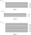
- FIG. 1 is a first schematic structural diagram of the package structure according to an embodiment of the present disclosure.
- the present disclosure provides the package structure 10.
- the package structure 10 includes an organic structural layer 101.
- a material of the organic structural layer 101 includes an organic structural material, and a structural formula of the organic structural material includes wherein, an R 1 group is an R 2 group is one or more of or -----O-----, n is a positive integer greater than or equal to 1, and x is one or more of -----H, ----SiH 3, or ---NH 2.
- the package structure 10 provided in the present disclosure includes the organic structural layer 101.
- the organic structural layer 101 includes the organic structural material.
- the organic structural material is an inorganic material having chain chemical bonds. Due to having the chain chemical bonds, the inorganic material has related properties of organic materials. For example, the organic structural material has lower stresses and better step-coverage properties.
- the organic structural layer 101 of the present disclosure obtains a material having organic properties by a manufacturing method of inorganic materials. Therefore, the organic structural layer 101 has buffering properties of organic encapsulation materials and water and oxygen blocking effects of inorganic encapsulation materials. Therefore, the package structure 10 of the present disclosure can obtain a better encapsulation effect, thereby improving encapsulation reliability of the display panel.
- Step coverage means a percentage of ratio of a thickness of a film layer across steps to a thickness of the film layer on a flat place.
- a thickness of the organic structural layer 101 ranges from 1 ⁇ m to 5 ⁇ m.
- the thickness of the organic structural layer 101 may be 1 ⁇ m, 1.5 ⁇ m, 2 ⁇ m, 2.5 ⁇ m, 3 ⁇ m, 3.5 ⁇ m, 4 ⁇ m, 4.5 ⁇ m, or 5 ⁇ m.
- the above numerical values are merely illustrative, and the thickness of the organic structural layer 101 may also be other values from 1 ⁇ m to 5 ⁇ m.
- the thickness of the organic structural layer 101 may be set according to encapsulation requirements.
- the R 1 group is the R 2 group is and/or -----O-----, n is the positive integer greater than or equal to 1, and x is one or more of -----H, ----SiH 3 , or ---NH 2 . That is, x in the R 1 group and the R 2 group may be any one selected from -----H, ----SiH 3 , and ---NH 2 .
- the R 2 group may also be -----O-----.
- the R 1 group and the R 2 group in the organic structural material may be two, three, or four kinds selected from the above groups.
- the organic structural material in the organic structural material, the R 1 group is --SiH 2 --, and the R 2 group is --NH--, then the organic structural material will include a structure of --SiH 2 -NH-SiH 2 -NH-SiH 2 - whilNH-SiH 2 -NH--.
- the R 1 group is --Si-- and --SiH 2 --, and the R 2 group is --NH--, then the organic structural material may include a structure of --Si-NH-SiH 2 -NH- whil-Si-NH--.
- the material of the organic structural layer further includes an inorganic material, and the inorganic material includes one or more combinations of silicon nitride, silicon oxide, or silicon oxynitride.
- the organic structural layer is manufactured by plasma enhanced chemical vapor deposition. Specifically, silane, ammonia, and water are introduced to be as reactive gases, and then the reactive gases are ionized by microwave or radio frequency to locally form plasma. A chemical activity of the plasma is very strong, so it is easy for the plasma to react and then form the organic structural layer.
- the organic structural material may also form a cross-linked structure with peripheral organic structural materials.
- the organic structural material and the inorganic material that specifically form are related to the reactive gases that are introduced.
- the inorganic material that is formed is silicon nitride
- the R 1 group is one or more of -----SiH 2 -- , or -----SiH 3
- the R 2 group is one or more of or
- the inorganic material that is formed being silicon oxide and silicon oxynitride and corresponding organic structural material thereof are similar to the above example and will not be repeated here.
- a molar ratio of the organic structural material to the inorganic material ranges from 0.01 to 0.75. Further, the molar ratio of the organic structural material to the inorganic material may range from 0.05 to 0.5.
- the organic structural material and the inorganic material are formed by a chemical reaction between different plasma groups that are ionized by microwave or radio frequency. In a case of introducing different gas flow rates, types and numbers of plasma groups generated by ionization will also be different.
- the molar ratio of the organic structural material to the inorganic material that are generated ranges from 0.01 to 0.75. That is, in the organic structural layer, a content of the organic structural material is 1 % to 75% of a content of the inorganic material.
- a ratio of the content of the organic structural material to the content of the inorganic material may be 0.01, 0.02, 0.03, 0.04, 0.05, 0.1, 0.15, 0.2, 0.25, 0.3, 0.35, 0.4, 0.45, 0.5, 0.55, 0.6, 0.65, 0.7, or 0.75.
- the above numerical values are merely illustrative, and the molar ratio of the organic structural material to the inorganic material may also be other values from 0.01 to 0.75.
- the ratio of the content of the organic structural material to the content of the inorganic material ranging from 0.01 to 0.75 can allow the organic structural layer to have properties of the organic materials and excellent encapsulation properties.
- the package structure 10 may only be provided with one organic structural layer 101 for encapsulation. Only the one organic structural layer 101 as the package structure 10 can reduce the thickness of the package structure 10. It can ensure bendability of panels when the organic structural layer 101 is applied to flexible display panels for encapsulation. Meanwhile, since there is only one layer of thin-film structure for encapsulation, the thickness of the package structure 10 is thinner at a bending site of the flexible display panels, thereby effectively reducing a bending radius, narrowing bezels, and preventing film layers from breaking at the bending site.
- the package structure 10 may also include at least one inorganic layer 102.
- a material of the at least one inorganic layer 102 includes one or more combinations of nitride, oxide, or nitrogen oxide.
- the nitride may be silicon nitride.
- the oxide may be aluminum oxide, silicon oxide, titanium oxide, zirconium oxide, or zinc oxide.
- the nitrogen oxide may be silicon oxynitride. Disposing the at least one inorganic layer 102 in the package structure 10, which combines the inorganic material and the material having the organic properties for encapsulation, can obtain a better encapsulation effect.
- the at least one inorganic layer 102 is used to block water and oxygen, and with the organic properties of the organic structural layer 101, the organic structural layer 101 is used as an organic layer to extend an intruding path of water vapor. Meanwhile, the organic structural layer 101 has good step-coverage properties and can well cover film layers that need to be encapsulated. Combining the organic structural layer 101 and the at least one inorganic layer 102 can improve an ability of the package structure 10 for blocking water and oxygen, thereby extending a service life of the display panel.
- a thickness of the at least one inorganic layer 102 ranges from 20 nm to 1500 nm.
- the thickness of the at least one inorganic layer 102 may be 20 nm, 300 nm, 400 nm, 500 nm, 600 nm, 700 nm, 800 nm, 900 nm, 1000 nm, 1100 nm, 1200 nm, 1300 nm, 1400 nm, or 1500 nm.
- the thickness of the at least one inorganic layer 102 may be adaptively set according to encapsulation requirements. For example, when the organic structural layer 101 needs to be set thinner, the thickness of the at least one inorganic layer 102 may be appropriately increased to ensure the encapsulation effect of the package structure.
- the package structure 10 includes two inorganic layers 102.
- the organic structural layer 101 is disposed between the two organic layers 102. Disposing the organic structural layer 101 between the two organic layers 102 can allow the two inorganic layers 102 to play a role of retaining walls. After the organic structural layer 101 absorbs water and oxygen, the inorganic layers 102 can block water and oxygen in the organic structural layer 101 to form a blocking space for water and oxygen, thereby preventing water and oxygen from intruding.
- This package structure 10 can further improve the ability for blocking water and oxygen and the encapsulation reliability.
- FIG. 2 is a second schematic structural diagram of the package structure according to an embodiment of the present disclosure.
- the package structure 10 shown in FIG. 2 includes one inorganic layer 102.
- the organic structural layer 101 may be disposed on either side of the inorganic layer 102. Combining the organic structural layer 101 and the inorganic layer 102 for encapsulation can improve the ability of the package structure 10 for blocking water and oxygen.
- FIG. 3 is a third schematic structural diagram of the package structure according to an embodiment of the present disclosure.
- the package structure 10 includes three inorganic layers 102 and two organic structural layers 101, and the three inorganic layers 102 and the two organic structural layers 101 are stacked alternatingly.
- film densities of the organic structural layers 101 and the inorganic layers 102 are not particularly high, multiple layers of the organic structural layers 101 and the inorganic layers 102 being stacked alternatingly for encapsulation can improve a density of the package structure 10, thereby better preventing water and oxygen from intruding.
- disposing the two organic structural layers 101 can extend the intruding path of water and oxygen.
- the inorganic layers 102 can block water and oxygen in the organic structural layers 101. Therefore, disposing a five-layered alternating stacked structure of the organic structural layers 101 and the inorganic layers 102 can further improve the encapsulation effect.
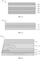
- FIG. 4 is a fourth schematic structural diagram of the package structure according to an embodiment of the present disclosure.
- the package structure 10 includes three inorganic layers 102, one organic structural layer 101, and an organic layer 103.
- the three inorganic layers 102, the organic structural layer 102, and the organic layer 103 are stacked in sequence in an order of one of the three inorganic layers, the organic structural layer, another one of the three inorganic layers, the organic layer, and yet another one of the three inorganic layers.
- a material of the organic layer 103 includes a UV-sensitive polymer, an epoxy polymer, or an acrylic polymer.
- the material of the organic layer 103 may be organic materials such as epoxy resin, polyimide (PI), polyethylene terephthalate (PET), polycarbonate (PC), polyethylene (PE), polyacrylate (PEA), or polymethylmethacrylate (PMMA).
- PI polyimide
- PET polyethylene terephthalate
- PC polycarbonate
- PE polyethylene
- PEA polyacrylate
- PMMA polymethylmethacrylate
- the organic layer 103 is made of the organic materials. Combining the organic structural layer 101 and the organic layer 103 in the package structure 10 can better extend the intruding path of water vapor and effectively block water and oxygen. In addition, a surface of the organic layer 103 is flatter, so an interface quality between the inorganic layers 102 and the organic layer 103 can be improved, thereby effectively preventing the film layers from falling off.
- FIG. 5 is a first schematic structural diagram of the display panel according to an embodiment of the present disclosure.
- the display panel 100 includes an array substrate 20, a light-emitting device layer 30, and the package structure 10.
- the light-emitting device layer 30 is disposed on the array substrate 20.
- the package structure 10 is disposed on one side of the light-emitting device layer 30 away from the array substrate 20.
- the package structure 10 is the package structure 10 mentioned above.
- FIG. 6 is a second schematic structural diagram of the display panel according to an embodiment of the present disclosure.
- the array substrate 20 includes a substrate 201 and a thin film transistor layer 202.
- the package structure 10 including a stacked structure of an inorganic layer 102/ an organic structural layer 101/ an inorganic layer 102 in FIG. 5 is taken as an example for description. Thicknesses and shapes of each of film layers in FIG. 5 are only for illustration and do not cause a limitation on the structure of the display panel 100.
- the substrate 201 may be glass, functional glass (sensor glass), or a flexible substrate.
- Specific film layers and assembly thereof of the thin film transistor layer 202 are technical means commonly used in the art and will not be repeated here.
- the display panel 100 provided in the present disclosure uses the package structure including the organic structural layer 101.
- the organic structural layer 101 includes the organic structural material.
- the organic structural material is the inorganic material having the chain chemical bonds. Due to having the chain chemical bonds, the inorganic material has related properties of organic materials. For example, the organic structural material has lower stresses and better step-coverage properties.
- the organic structural layer 101 of the present disclosure obtains the material having organic properties by the manufacturing method of inorganic materials.
- the organic structural layer 101 improves the water and oxygen blocking effect of the organic encapsulation materials. Therefore, the package structure 10 of the present disclosure can allow the display panel 100 to obtain the better encapsulation effect, thereby improving the encapsulation reliability of the display panel 100.
- the package structure 10 in addition to applying to encapsulation of the display panel 100, can also be applied to related aspects of step coverage of other electronic components. For example, it may be applied to electronic components having an undercut structure and used to cover steps formed due to the undercut structure.
- FIG. 7 is a flowchart of the manufacturing method of the display panel according to an embodiment of the present disclosure.
- the manufacturing method of the display panel specifically includes following steps.
- Step 11 providing the array substrate.
- the array substrate may include the substrate and the thin film transistor layer disposed on the substrate.
- the substrate may be glass, functional glass (sensor glass), or the flexible substrate.
- the functional glass is obtained by sputtering a transparent metal oxide conductive thin film on ultra-thin glass and annealing at a high temperature.
- the thin film transistor layer is manufactured on the substrate.
- a specific manufacturing method of the thin film transistor layer is technical means commonly used in the art and will not be repeated here.
- Step 12 disposing the light-emitting device layer on the array substrate.
- Step 13 transferring the array substrate provided with the light-emitting device layer into a cavity and introducing reactive gases into the cavity.
- the reactive gases include a silane gas (SiH 4 ) and a nitrous oxide gas (N 2 O) or include the silane gas and ammonia (NH 3 ).
- the reactive gases are partially ionized by increasing flow rates of the reactive gases that are introduced. Specifically, compared to flow rates of generating ordinary inorganic silicon nitride materials, silicon oxide materials, and silicon oxynitride materials, the gas flow rates will be increased by 3 to 7 times when used to generate the organic structural material. Increasing the flow rates of the reactive gases can partially ionize the reactive gases on one hand and can increase a film formation speed on another hand.
- Step 14 ionizing the reactive gases to form reactive plasma.
- the reactive gases can be ionized by microwave or radio frequency.
- adjusting a gas pressure and a radio frequency power in the cavity to ionize the reactive gases by radio frequency adjusting a gas pressure and a radio frequency power in the cavity to ionize the reactive gases by radio frequency.
- the gas pressure may range from 800 millitorr to 2000 millitorr.
- the radio frequency power may range from 1 KW to 2 KW.
- Step 15 the reactive plasma undergoing a chemical reaction and being deposited on the light-emitting device layer to form the organic structural layer.
- the material of the organic structural layer includes the organic structural material, and the organic structural material includes wherein, the R 1 group is the R 2 group is one or more of or -----O-----, n is a positive integer greater than or equal to 1, and x is one or more of -----H, ----SiH 3 , or ---NH 2 .
- the present disclosure uses plasma enhanced chemical vapor deposition (PECVD) to manufacture the organic structural layer, so a manufacturing temperature is low, which will not affect the light-emitting device layer, thereby ensuring luminous efficiency of the light-emitting device layer.
- PECVD plasma enhanced chemical vapor deposition
- using the method of manufacturing inorganics to form the material having the organic properties can use the organic structural layer to replace film layers formed by the organic materials for encapsulation. It is not necessary to manufacture organic film layers by ink-jet printing, thereby preventing overflow of materials during ink-jet printing.
- the PECVD method has a fast deposition rate, and good film-forming quality, so the package structure formed has less micropores and less cracking, thereby ensuring a better encapsulation effect.
- the method further includes a step of depositing the inorganic layer on one side of the light-emitting device layer away from the array substrate.
- the inorganic layer may be disposed on one side of the organic structural layer adjacent to the light-emitting device layer, or the inorganic layer may also be disposed on one side of the organic structural layer away from the light-emitting device layer. Or the inorganic layer may be disposed on both sides of the organic structural layer at a same time.
- the inorganic layer may be set in one layer or multiple layers.
- the inorganic layer being disposed on the side of the organic structural layer adjacent to the light-emitting device layer is taken as an example for description.
- the inorganic layer is deposited on the light-emitting device layer by chemical vapor deposition (CVD), atomic layer deposition (ALD), or plasma enhanced chemical vapor deposition.
- CVD chemical vapor deposition
- ALD atomic layer deposition
- plasma enhanced chemical vapor deposition plasma enhanced chemical vapor deposition.
- the silicon nitride material is used as the inorganic layer
- the array substrate provided with the light-emitting device layer is transferred to the cavity, and the silane gas and ammonia are introduced.
- the inorganic layer manufactured by PECVD has a fast manufacture speed, a dense film layer, and good adhesion.
- the organic structural layer can be subsequently manufactured by PECVD in a same cavity. In this way, there is no need to transfer the array substrate after the inorganic layer is manufactured, thereby preventing film layers from breaking during a transfer process and being able to speed up production.
- another inorganic layer may also be manufactured subsequently by PECVD in the same cavity, thereby forming a stacked package structure of an inorganic barrier/ an organic buffering layer/ an inorganic barrier.
- the organic structural layer may continue to be produced by the silane gas and ammonia. It can be manufactured only by increasing the gas flow rates to 3 to 7 times that of the inorganic layer and then ionized. In this way, the gases in the cavity are same, and other impurity will not be produced, so the package structure manufactured has high film purity and less defects, thereby being more beneficial to improve the encapsulation effect.
- another silicon nitride inorganic layer can be manufactured by reducing the gas flow rates.
- the introduction of silane gas and ammonia is used as an example.
- gases introduced when manufacturing the inorganic layer and the organic structural layer may also not be exactly the same.
- the method further includes a step of depositing the organic layer on one side of the inorganic layer away from the array substrate.
- the organic layer may be disposed on one side of the inorganic layer adjacent to the light-emitting device layer, or the organic layer may also be disposed between the organic structural layer and the inorganic layer. Or the organic layer may be disposed between two inorganic layers.
- the organic layer may be set in one layer or multiple layers. Positions of the organic structural layer, the inorganic layer, and the organic layer are not limited in the present disclosure.
- the organic layer is manufactured by ink-jet printing or evaporation.
- a film-forming method of evaporation is simple, a film layer formed thereof is thin and has high purity and density. Film forming areas can be accurately controlled by ink-jet printing, thereby saving materials, reducing costs, and improving product yields.
- the manufacturing method of the display panel provided in the present disclosure can manufacture the inorganic layer and the organic structural layer having the organic material properties in the same cavity by manufacturing the inorganic layer using CVD and manufacturing the organic structural layer using PECVD.
- the manufacturing method of the display panel can reduce transfer of the substrate during encapsulation, thereby preventing the package structure or the substrate from breaking during the transfer process and therefore improving product yields of the display panel.
Landscapes
- Chemical & Material Sciences (AREA)
- Engineering & Computer Science (AREA)
- Organic Chemistry (AREA)
- Chemical Kinetics & Catalysis (AREA)
- Materials Engineering (AREA)
- Medicinal Chemistry (AREA)
- Polymers & Plastics (AREA)
- Health & Medical Sciences (AREA)
- Life Sciences & Earth Sciences (AREA)
- Wood Science & Technology (AREA)
- Inorganic Chemistry (AREA)
- Manufacturing & Machinery (AREA)
- Microelectronics & Electronic Packaging (AREA)
- Physics & Mathematics (AREA)
- Optics & Photonics (AREA)
- Electroluminescent Light Sources (AREA)
- Devices For Indicating Variable Information By Combining Individual Elements (AREA)
Applications Claiming Priority (2)
| Application Number | Priority Date | Filing Date | Title |
|---|---|---|---|
| CN202110847538.6A CN113629210B (zh) | 2021-07-27 | 2021-07-27 | 封装结构、显示面板及显示面板的制作方法 |
| PCT/CN2021/110221 WO2023004839A1 (zh) | 2021-07-27 | 2021-08-03 | 封装结构、显示面板及显示面板的制作方法 |
Publications (2)
| Publication Number | Publication Date |
|---|---|
| EP4380337A1 true EP4380337A1 (de) | 2024-06-05 |
| EP4380337A4 EP4380337A4 (de) | 2025-08-06 |
Family
ID=78381026
Family Applications (1)
| Application Number | Title | Priority Date | Filing Date |
|---|---|---|---|
| EP21819016.3A Pending EP4380337A4 (de) | 2021-07-27 | 2021-08-03 | Verpackungsstruktur, anzeigetafel und verfahren zur herstellung einer anzeigetafel |
Country Status (6)
| Country | Link |
|---|---|
| US (1) | US20240065075A1 (de) |
| EP (1) | EP4380337A4 (de) |
| JP (1) | JP7499776B2 (de) |
| KR (2) | KR20250004128A (de) |
| CN (1) | CN113629210B (de) |
| WO (1) | WO2023004839A1 (de) |
Families Citing this family (3)
| Publication number | Priority date | Publication date | Assignee | Title |
|---|---|---|---|---|
| CN114171702B (zh) * | 2021-12-03 | 2023-11-28 | 深圳市华星光电半导体显示技术有限公司 | Oled封装结构与oled封装方法 |
| CN114566091B (zh) * | 2022-02-28 | 2023-12-29 | 京东方科技集团股份有限公司 | 显示模组及其制备方法、显示装置 |
| CN115020608A (zh) * | 2022-05-31 | 2022-09-06 | 固安翌光科技有限公司 | 一种发光装置 |
Family Cites Families (9)
| Publication number | Priority date | Publication date | Assignee | Title |
|---|---|---|---|---|
| JP3370408B2 (ja) * | 1993-12-28 | 2003-01-27 | 東燃ゼネラル石油株式会社 | セラミックコーティングの製造方法 |
| US9404178B2 (en) * | 2011-07-15 | 2016-08-02 | Applied Materials, Inc. | Surface treatment and deposition for reduced outgassing |
| JP2013077460A (ja) | 2011-09-30 | 2013-04-25 | Toppan Printing Co Ltd | 有機elパネルの製造方法、有機elパネル及び有機elディスプレイ |
| CN107768534A (zh) * | 2016-08-19 | 2018-03-06 | 上海和辉光电有限公司 | 一种柔性oled的薄膜封装结构及其制备方法 |
| CN107845734A (zh) * | 2016-09-19 | 2018-03-27 | 上海和辉光电有限公司 | 一种薄膜封装材料、薄膜封装结构和oled显示面板 |
| CN107845733A (zh) * | 2016-09-19 | 2018-03-27 | 上海和辉光电有限公司 | 一种薄膜封装结构和oled显示面板 |
| CN107845732A (zh) * | 2016-09-19 | 2018-03-27 | 上海和辉光电有限公司 | 一种薄膜封装结构和oled显示面板 |
| CN108206242A (zh) * | 2016-12-19 | 2018-06-26 | 上海和辉光电有限公司 | 柔性oled显示屏的封装结构及其制备方法 |
| CN109860423A (zh) * | 2019-02-20 | 2019-06-07 | 湖畔光电科技(江苏)有限公司 | 一种oled顶发射的封装结构及制备方法 |
-
2021
- 2021-07-27 CN CN202110847538.6A patent/CN113629210B/zh active Active
- 2021-08-03 JP JP2021547103A patent/JP7499776B2/ja active Active
- 2021-08-03 WO PCT/CN2021/110221 patent/WO2023004839A1/zh not_active Ceased
- 2021-08-03 EP EP21819016.3A patent/EP4380337A4/de active Pending
- 2021-08-03 US US17/598,849 patent/US20240065075A1/en active Pending
- 2021-08-03 KR KR1020247040895A patent/KR20250004128A/ko active Pending
- 2021-08-03 KR KR1020217029572A patent/KR20230018290A/ko not_active Ceased
Also Published As
| Publication number | Publication date |
|---|---|
| JP7499776B2 (ja) | 2024-06-14 |
| CN113629210A (zh) | 2021-11-09 |
| KR20230018290A (ko) | 2023-02-07 |
| EP4380337A4 (de) | 2025-08-06 |
| CN113629210B (zh) | 2024-06-11 |
| WO2023004839A1 (zh) | 2023-02-02 |
| JP2023538465A (ja) | 2023-09-08 |
| US20240065075A1 (en) | 2024-02-22 |
| KR20250004128A (ko) | 2025-01-07 |
Similar Documents
| Publication | Publication Date | Title |
|---|---|---|
| US11978803B2 (en) | Flexible display and method of manufacturing the same | |
| CN101697343B (zh) | 一种薄膜封装方法 | |
| EP4380337A1 (de) | Verpackungsstruktur, anzeigetafel und verfahren zur herstellung einer anzeigetafel | |
| US9831466B2 (en) | Method for depositing a multi-layer moisture barrier on electronic devices and electronic devices protected by a multi-layer moisture barrier | |
| CN106450035A (zh) | 一种显示面板及其制备方法 | |
| CN104051652B (zh) | 一种柔性薄膜晶体管 | |
| US8975534B2 (en) | Flexible base material and flexible electronic device | |
| CN107403877A (zh) | Oled面板的封装方法 | |
| CN105190932A (zh) | 用于薄膜封装的n2o稀释工艺对阻挡膜性能的改进 | |
| CN104766890B (zh) | 薄膜晶体管及其制造方法和应用 | |
| JP2009274251A (ja) | 透明バリアフィルムおよびその製造方法 | |
| US20150129989A1 (en) | Gate insulating layer and method for forming the same | |
| WO2019022929A1 (en) | ENHANCED THIN FILM ENCAPSULATION | |
| CN103500800A (zh) | 显示面板、显示装置及显示面板的制作方法 | |
| CN1563243A (zh) | 一种高热导性和高气密性的薄膜封装材料及其制备方法 | |
| US11991917B2 (en) | Display panel and manufacturing method thereof | |
| CN107845732A (zh) | 一种薄膜封装结构和oled显示面板 | |
| Chen | Realizing Thin‐Film Encapsulation's Benefits for Large‐Scale OLED Panels | |
| KR20190127086A (ko) | 기체 차단용 필름 및 이의 제조방법 | |
| CN107845733A (zh) | 一种薄膜封装结构和oled显示面板 | |
| CN105957978B (zh) | 封装结构及其制造方法 | |
| WO2019067137A1 (en) | THIN LAYER ENCAPSULATION DIFFUSION LAYER BY PECVD | |
| WO2012132585A1 (ja) | ガスバリア膜、その製造装置、及びその製造プログラム | |
| CN109487242B (zh) | 薄膜沉积设备及薄膜沉积方法、显示装置 | |
| US20240023409A1 (en) | Display panel and method of manufacturing the same |
Legal Events
| Date | Code | Title | Description |
|---|---|---|---|
| STAA | Information on the status of an ep patent application or granted ep patent |
Free format text: STATUS: UNKNOWN |
|
| STAA | Information on the status of an ep patent application or granted ep patent |
Free format text: STATUS: THE INTERNATIONAL PUBLICATION HAS BEEN MADE |
|
| PUAI | Public reference made under article 153(3) epc to a published international application that has entered the european phase |
Free format text: ORIGINAL CODE: 0009012 |
|
| STAA | Information on the status of an ep patent application or granted ep patent |
Free format text: STATUS: REQUEST FOR EXAMINATION WAS MADE |
|
| 17P | Request for examination filed |
Effective date: 20211213 |
|
| AK | Designated contracting states |
Kind code of ref document: A1 Designated state(s): AL AT BE BG CH CY CZ DE DK EE ES FI FR GB GR HR HU IE IS IT LI LT LU LV MC MK MT NL NO PL PT RO RS SE SI SK SM TR |
|
| DAV | Request for validation of the european patent (deleted) | ||
| DAX | Request for extension of the european patent (deleted) | ||
| A4 | Supplementary search report drawn up and despatched |
Effective date: 20250709 |
|
| RIC1 | Information provided on ipc code assigned before grant |
Ipc: H10K 50/00 20230101AFI20250703BHEP Ipc: C09D 183/08 20060101ALI20250703BHEP Ipc: C09D 183/14 20060101ALI20250703BHEP Ipc: C09D 183/16 20060101ALI20250703BHEP Ipc: H01L 21/02 20060101ALI20250703BHEP |