EP4361901A1 - Supraleitende quantenschaltung und herstellungsverfahren dafür sowie quantencomputer - Google Patents
Supraleitende quantenschaltung und herstellungsverfahren dafür sowie quantencomputer Download PDFInfo
- Publication number
- EP4361901A1 EP4361901A1 EP22882866.1A EP22882866A EP4361901A1 EP 4361901 A1 EP4361901 A1 EP 4361901A1 EP 22882866 A EP22882866 A EP 22882866A EP 4361901 A1 EP4361901 A1 EP 4361901A1
- Authority
- EP
- European Patent Office
- Prior art keywords
- superconducting
- superconducting element
- quantum circuit
- electrode
- superconducting quantum
- Prior art date
- Legal status (The legal status is an assumption and is not a legal conclusion. Google has not performed a legal analysis and makes no representation as to the accuracy of the status listed.)
- Withdrawn
Links
Images


Classifications
-
- H—ELECTRICITY
- H10—SEMICONDUCTOR DEVICES; ELECTRIC SOLID-STATE DEVICES NOT OTHERWISE PROVIDED FOR
- H10N—ELECTRIC SOLID-STATE DEVICES NOT OTHERWISE PROVIDED FOR
- H10N69/00—Integrated devices, or assemblies of multiple devices, comprising at least one superconducting element covered by group H10N60/00
-
- G—PHYSICS
- G06—COMPUTING OR CALCULATING; COUNTING
- G06N—COMPUTING ARRANGEMENTS BASED ON SPECIFIC COMPUTATIONAL MODELS
- G06N10/00—Quantum computing, i.e. information processing based on quantum-mechanical phenomena
-
- H—ELECTRICITY
- H10—SEMICONDUCTOR DEVICES; ELECTRIC SOLID-STATE DEVICES NOT OTHERWISE PROVIDED FOR
- H10N—ELECTRIC SOLID-STATE DEVICES NOT OTHERWISE PROVIDED FOR
- H10N60/00—Superconducting devices
- H10N60/01—Manufacture or treatment
- H10N60/0912—Manufacture or treatment of Josephson-effect devices
-
- G—PHYSICS
- G06—COMPUTING OR CALCULATING; COUNTING
- G06N—COMPUTING ARRANGEMENTS BASED ON SPECIFIC COMPUTATIONAL MODELS
- G06N10/00—Quantum computing, i.e. information processing based on quantum-mechanical phenomena
- G06N10/20—Models of quantum computing, e.g. quantum circuits or universal quantum computers
-
- G—PHYSICS
- G06—COMPUTING OR CALCULATING; COUNTING
- G06N—COMPUTING ARRANGEMENTS BASED ON SPECIFIC COMPUTATIONAL MODELS
- G06N10/00—Quantum computing, i.e. information processing based on quantum-mechanical phenomena
- G06N10/40—Physical realisations or architectures of quantum processors or components for manipulating qubits, e.g. qubit coupling or qubit control
-
- H—ELECTRICITY
- H01—ELECTRIC ELEMENTS
- H01P—WAVEGUIDES; RESONATORS, LINES, OR OTHER DEVICES OF THE WAVEGUIDE TYPE
- H01P7/00—Resonators of the waveguide type
- H01P7/06—Cavity resonators
- H01P7/065—Cavity resonators integrated in a substrate
-
- H—ELECTRICITY
- H10—SEMICONDUCTOR DEVICES; ELECTRIC SOLID-STATE DEVICES NOT OTHERWISE PROVIDED FOR
- H10N—ELECTRIC SOLID-STATE DEVICES NOT OTHERWISE PROVIDED FOR
- H10N60/00—Superconducting devices
- H10N60/10—Junction-based devices
- H10N60/12—Josephson-effect devices
-
- H—ELECTRICITY
- H10—SEMICONDUCTOR DEVICES; ELECTRIC SOLID-STATE DEVICES NOT OTHERWISE PROVIDED FOR
- H10N—ELECTRIC SOLID-STATE DEVICES NOT OTHERWISE PROVIDED FOR
- H10N60/00—Superconducting devices
- H10N60/80—Constructional details
- H10N60/805—Constructional details for Josephson-effect devices
Definitions
- the present application belongs to the field of quantum information, in particular to the field of quantum computing technology.
- the present application relates to a superconducting quantum circuit and a fabrication method thereof, as well as a quantum computer.
- Quantum computing is a new type of computing method that combines quantum mechanics and computer science, which follows the laws of quantum mechanics and regulates quantum information units for calculation. It takes the qubits composed of microscopic particles as basic units, with the characteristics of quantum superposition and entanglement. Moreover, through the controlled evolution of quantum states, quantum computing is able to realize information encoding and computational storage, with a huge information carrying capacity and excellent parallel computing processing capabilities with which classical computing technologies are incomparable. With the increase of the number of qubits, the computing and storage capacity thereof will expand exponentially. This is one of the key development directions in the field of quantum information technology.
- the structure of the superconducting quantum circuit in the related art brings numerous inconveniences to the fabrication of the superconducting quantum circuit.
- the superconducting quantum interference device and another superconducting element are relatively independent, which makes it often necessary to prepare one of the above two structures, and then prepare the other one of the above two structures.
- the present application provides a superconducting quantum circuit and a fabrication method thereof, as well as a quantum computer, to enable efficient process fabrication.
- One embodiment of the present application provides a superconducting quantum circuit, comprising a first superconducting element and a second superconducting element formed on a substrate, and a superconducting quantum interference device located between the first superconducting element and the second superconducting element, wherein the superconducting quantum interference device comprises:
- the first superconducting element is a ground layer and the second superconducting element is a capacitor plate having a capacitive effect with respect to the ground layer.
- the capacitor plate comprises at least two sub-capacitor plates, and one of the at least two sub-capacitor plates is integrally connected to the bottom electrode.
- each of the first superconducting element and the second superconducting element is a capacitor plate having a capacitive effect with respect to the ground layer.
- the capacitor plates each comprises at least two sub-capacitor plates, and one of the at least two sub-capacitor plates is integrally connected to the bottom electrode, or integrally connected to the top electrode.
- the at least two sub-capacitor plates are separated from each other.
- the superconducting quantum interference device comprises at least two top electrodes.
- the at least two top electrodes are parallel or not parallel to each other.
- the Josephson junction is a tunnel junction or other structure exhibiting a Josephson effect.
- the superconducting quantum circuit further comprises a third superconducting element located at a same surface as the first superconducting element and the second superconducting element.
- the third superconducting element is at least one of a read resonant cavity, a pulse control line, a flux-modulation signal line, and a read signal line.
- a second embodiment of the present application provides a fabrication method for a superconducting quantum circuit, wherein the superconducting quantum circuit comprises a first superconducting element and a second superconducting element formed on a substrate, and a superconducting quantum interference device located between the first superconducting element and the second superconducting element, and the fabrication method comprises:
- a step of patterning the superconducting material layer formed on the substrate to obtain the first superconducting element, the second superconducting element, and the first electrode integrally connected to the second superconducting element comprises:
- a step of forming the top electrode that is electrically connected at one end to the first superconducting element and forms the partial overlapping area with the barrier layer comprises:
- a third embodiment of the present application provides a quantum computer, comprising the superconducting quantum circuit, or comprising the superconducting quantum circuit fabricated by the fabrication method.
- the superconducting quantum circuit comprises a first superconducting element, a second superconducting element formed on a substrate, and a superconducting quantum interference device located between the first superconducting element and the second superconducting element, and the superconducting quantum interference device comprises: a bottom electrode integrally connected to the second superconducting element, a barrier layer located on the bottom electrode and a top electrode that is electrically connected at one end to the first superconducting element, and forms a partial overlapping area with the barrier layer to obtain a Josephson junction at the overlapping area.
- the bottom electrode and the second superconducting element which are integrally connected in the superconducting quantum circuit provided by the present application, can be fabricated by one patterning process. After the barrier layer is formed on the surface of the bottom electrode, the top electrode partially overlapped with the barrier layer and electrically connected at one end to the first superconducting element can be obtained by one more process such as evaporation coating.
- the structure of the superconducting quantum circuit provided in the present application facilitates fabrication and helps to shorten the process flow and improve the fabrication efficiency.
- the qubits in terms of physical realization, include superconducting quantum circuits, semiconductor quantum dots, ion traps, diamond vacancies, topological quanta, photons, and so on.
- Superconducting quantum computing is the fastest and best way to realize solid-state quantum computing. Since the energy level structure of superconducting quantum circuits can be regulated by applying electromagnetic signals externally, the design and customization of the circuits are highly controllable. At the same time, thanks to the existing mature process of integrated circuits, the superconducting quantum circuits have a scalability that is incomparable by most quantum physics systems.
- qubits in the superconducting quantum computing can be anharmonic oscillatory circuits with superconducting elements and capacitors.
- the capacitor is often a capacitor to ground, e.g., a cross-shaped parallel-plate capacitor.
- the superconducting element may be a superconducting quantum interference device grounded at one end and connected to the capacitor at the other end.
- FIG. 1 shows a schematic structural diagram of a qubit on a superconducting quantum chip in the related art.
- a capacitor plate C q is surrounded by a ground layer (GND) and there is a gap between the capacitor plate C q and the ground layer (GND), and a superconducting quantum interference device (Squid) is connected to the capacitor plate C q at one end, and to the ground layer (GND) at the other end.
- GND ground layer
- Squid superconducting quantum interference device
- the capacitor plate of each qubit usually adopts a cross-shaped capacitor plate, a first end of the cross-shaped capacitor plate is usually used for connecting a superconducting quantum interference device Squid, and a second end of the cross-shaped capacitor plate opposite the first end is used for coupling to a read resonant cavity.
- a certain space is required to be reserved near the first end and the second end for wiring, e.g., a space is required to be reserved near the first end for arranging pulse control lines (also called XY signal lines) and flux-modulation signal lines (also called Z signal lines).
- the other two ends of the cross-shaped capacitor plate, except the first and second ends described above, are used for coupling to neighboring qubits.
- the superconducting quantum interference device and another superconducting element are relatively independent, which makes it often necessary to prepare one of the above two structures, and then prepare the other one of the above two structures, thus bringing many inconveniences to the fabrication of the superconducting quantum circuit.
- the present application provides a superconducting quantum circuit and a fabrication method thereof, as well as a quantum computer, to address the deficiencies in the prior art.
- the superconducting quantum circuit of the present application has a bottom electrode and a second superconducting element integrally connected, and the bottom electrode and the second superconducting element which are integrally connected can be synchronously fabricated by one patterning process during a fabrication process. After a barrier layer is formed on the surface of the obtained bottom electrode, one process such as evaporation coating is only required to obtain a top electrode which is partially overlapped with the barrier layer and electrically connected to the first superconducting element at one end. Then the superconducting quantum circuit in the present application can also be obtained.
- the solution provided in the present application helps to shorten the fabrication process flow of the superconducting quantum circuits and realizes a more highly efficient process of fabrication.
- FIG. 2A , FIG. 2B , FIG. 2C , and FIG. 2D are schematic diagrams of a fabrication process of a superconducting quantum circuit provided by the present application, wherein FIG. 2D better illustrates the structure of a superconducting quantum circuit provided by the present application.
- M, N, and P are additionally schematically enlarged in the drawings of the present application.
- the present application provides a superconducting quantum circuit, which comprises a first superconducting element, a second superconducting element formed on a substrate 1, and a superconducting quantum interference device located between the first superconducting element and the second superconducting element, wherein the superconducting quantum interference device comprises:
- the other end of the top electrode 31 is connected to the barrier layer 242.
- the bottom electrode 241 of the superconducting quantum interference device is integrally connected with the second superconducting element, the bottom electrode 241 and the second superconducting element which are integrally connected are easy to be synchronously fabricated by one patterning process, and the bottom electrode 241 and the second superconducting element in this form have a good electrical connection performance.
- the barrier layer 242 is formed on the surface of the bottom electrode 241, one process such as evaporation coating is only required to obtain the top electrode 31 which is partially overlapped with the barrier layer 242 and electrically connected to the first superconducting element at one end.
- the structure of the superconducting quantum circuit facilitates fabrication and helps to shorten the process flow and improve the fabrication efficiency.
- the bottom electrode 241 and the second superconducting element can be connected in direct contact or can be integrally connected by means of an electrical connection part 23 formed synchronously with the second superconducting element and the bottom electrode 241. That is, the electrical connection part 23 may be formed synchronously when the second superconducting element and the bottom electrode 241 are formed. That is, the second superconducting element, the bottom electrode 241 and the electrical connection part 23 are integrally connected.
- the first superconducting element is a ground layer 21, and the second superconducting element is a capacitor plate 22 having a capacitance effect with respect to the ground layer 21.
- the capacitor plate 22 is not directly connected to the ground layer 21, and there is a proper gap between the capacitor plate 22 and the ground layer 21.
- the physical size of the gap is designed and determined according to the needs of the performance parameters of the quantum computing circuit.
- a capacitance C is formed between the capacitor plate 22 and the ground layer 21, thereby forming a circuit structure of qubits in the form of a single superconducting island, i.e., ground layer (GND) - superconducting quantum interference device - capacitor plate.
- the capacitor plate 22 is surrounded by the ground layer 21 and separated from the ground layer 21 by a gap exposing the surface of the substrate 1, which may be a dielectric substrate such as silicon or sapphire.
- the ground layer 21, the capacitor plate 22, and the superconducting quantum interference device are formed on a silicon substrate.
- the capacitor plate 22 and the ground layer 21 may be formed of superconducting materials exhibiting superconducting characteristics at a temperature equal to or lower than a critical temperature, such as aluminum, niobium or titanium nitride, which is not limited. Materials exhibiting superconducting characteristics at a temperature equal to or lower than a critical temperature may be used to form structures such as the ground layer 21, the capacitor plate 22, and the like.
- a critical temperature such as aluminum, niobium or titanium nitride
- FIG. 3A shows a schematic structural diagram of a first superconducting quantum circuit provided by the present application.
- the capacitor plate 22 comprises at least two sub-capacitor plates and one of the at least two sub-capacitor plates is integrally connected to the bottom electrode 241.
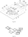
- the capacitor plate 22 is divided into a first sub-capacitor plate 221, a second sub-capacitor plate 222 and a third sub-capacitor plate 223 to form a plurality of capacitance effects, that is, a capacitance effect is formed between the first sub-capacitor plate 221 and the second sub-capacitor plate 222, and a capacitance effect is formed between the first sub-capacitor plate 221 and the third sub-capacitor plate 223.
- the first sub-capacitor plate 221 connected to the bottom electrode 241 adopts a structure integrally molded with the bottom electrode 241. In the structure with thin film limit, the contribution of the thickness to the capacitive effect can be ignored.
- the capacitor plate 22 in the qubit structure is divided and arranged into a plurality of sub-capacitor plates such that the capacitance in the qubit varies with the areas of the sub-capacitor plates. For example, the larger the area of a sub-capacitor plate is, the larger the capacitance of that sub-capacitor plate is. Accordingly, the capacitance of the qubits also varies with the number of sub-capacitor plates, and is related to the capacitance of each sub-capacitor plate, and the connection relationship between the sub-capacitor plates.
- the change in capacitance in the qubits in turn affects the resonant frequency of the qubits.
- the capacitance value of the qubit can be reduced by dividing the capacitor plate 22, that is, a plurality of sub-capacitor plates are obtained by dividing the capacitor plate 22, and the plurality of sub-capacitor plates are connected in series, so as to reduce the capacitance value of the qubit.
- it corresponds to a plurality of capacitors connected in series when the capacitor plate 22 is divided into a plurality of independent sub-capacitor plates, and the capacitance of the qubit is determined by these capacitors in series.
- the superconducting quantum circuits provided in the present application are not limited to the embodiment in which the first superconducting element is the ground layer 21 and the second superconducting element is the capacitor plate 22 with a capacitive effect relative to the ground layer 21. Some other embodiments of the superconducting quantum circuits provided in the present application are described below in conjunction with the drawings.
- FIG. 3B shows a schematic structural diagram of a second superconducting quantum circuit provided by the present application.
- each of the first superconducting element and the second superconducting element is a capacitor plate 22 having a capacitive effect with respect to the ground layer 21.
- FIG. 3B a ground layer 21 is formed on the substrate 1, and each of the first superconducting element and the second superconducting element is a capacitor plate 22 having a capacitive effect with respect to the ground layer 21.
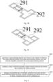
- the first superconducting element is a first capacitor plate 291 having a capacitive effect with respect to the ground layer 21
- the second superconducting element is a second capacitor plate 292 having a capacitive effect with respect to the ground layer 21, thereby forming a circuit structure of qubits in the form of having two superconducting islands, i.e., capacitor plate - superconducting quantum interference device - capacitor plate.
- FIG. 3C shows a schematic structural diagram of a third superconducting quantum circuit provided by the present application.
- the first capacitor plate 291 and the second capacitor plate 292 each comprises at least two sub-capacitor plates, and one of the at least two sub-capacitor plates is integrally connected to the bottom electrode 241, or integrally connected to the top electrode 31.
- the second capacitor plate 292 is divided into a plurality of sub-capacitor plates to form a plurality of capacitance effects, and similarly, the first capacitor plate 291 can be divided into a plurality of sub-capacitor plates (not shown in the Figure).
- the sub-capacitor plate connected to the top electrode 31 adopts a structure integrally molded with the top electrode 31, and the sub-capacitor plate connected to the bottom electrode 241 adopts a structure integrally molded with the bottom electrode 241.
- At least two sub-capacitor plates forming the same capacitor plate may be in the form of a structure separated from each other or in the form of a structure having an electrical connection.
- the superconducting quantum interference device comprises at least two top electrodes 31, wherein a different number of the top electrodes 31 results in a different number of Josephson junctions included in the superconducting quantum interference device, i.e., superconducting quantum interference devices with different structural forms and different magnetic flux sensitivity can be fabricated by adjusting the number of top electrodes 31.
- the at least two top electrodes 31 may be parallel or not parallel to each other.
- the at least two top electrodes 31 forms at least two partial overlapping area with the barrier layer 242, and the overlapping areas are different from each other.
- the different overlapping areas realize different critical currents of formed Josephson junctions, so that a superconducting quantum interference device comprising non-symmetric Josephson junctions can be obtained, and thus the frequency spectrum of the superconducting quantum circuit has at least two magnetic flux insensitive points.
- the superconducting quantum interference device comprises an odd number of the top electrodes 31, and the area of the overlapping area where each top electrode 31 partially overlaps with the barrier layer 242 is the same. This structural form also allows the frequency spectrum of the superconducting quantum circuit to have at least two magnetic flux insensitive points.
- the superconducting quantum circuit further comprises a third superconducting element fabricated in synchronization with the first superconducting element, the third superconducting element is located at a same surface as the first superconducting element and the second superconducting element, i.e., they are all located at the surface of the substrate 1.
- the third superconducting element is at least one of a read resonant cavity 34, a pulse control line 32, a flux-modulation signal line 33, and a read signal line.
- FIG. 4 shows a flowchart of a fabrication method of a superconducting quantum circuit provided by the present application.
- the superconducting quantum circuit comprises a first superconducting element and a second superconducting element formed on a substrate 1, and a superconducting quantum interference device located between the first superconducting element and the second superconducting element, the fabrication method comprises steps S401 to step S403, wherein:
- a first superconducting element, a second superconducting element, and a first electrode are firstly fabricated synchronously by a patterning process, and the first electrode is integrally connected to the second superconducting element.
- one process such as evaporation coating is only required to obtain a top electrode which is partially overlapped with the barrier layer and electrically connected at one end to the first superconducting element.
- the present application can reduce the times of evaporation coating, shorten the process flow and improve the fabrication efficiency.
- the fabrication method for the superconducting quantum circuit provided in the present application does not impose any requirement on the angle of the evaporation coating in the fabrication process to obtain the Josephson junction.
- a slant evaporation can be used or a vertical evaporation relative to the surface to be evaporated can be used.
- a plurality of Josephson junctions or a plurality of superconducting quantum circuits provided in the present embodiment can be fabricated synchronously.
- the bottom electrodes of a plurality of Josephson junctions and the top electrodes of a plurality of Josephson junctions are not limited to parallel structures.
- step S401 patterning the superconducting material layer 2 formed on the substrate 1 to obtain the first superconducting element, the second superconducting element, and the first electrode 24 integrally connected to the second superconducting element, specifically comprises steps S4011 to S4012, wherein:
- step S403, forming the top electrode 31 that is electrically connected at one end to the first superconducting element, and forms the partial overlapping area with the barrier layer 242 to obtain the Josephson junction at the overlapping area specifically comprises steps S4031 to S4032, wherein:
- a first region 25 for fabricating a read resonant cavity, a second region 26 for fabricating a pulse signal line, a third region 27 for fabricating a flux-modulation signal line, and a fourth region 28 for fabricating a coupling structure between adjacent bits can be obtained synchronously by etching.
- the top electrode 31 it is also possible to synchronously obtain the read resonant cavity 34, the pulse signal line 32, the flux-modulation signal line 33, and the coupling structure 35 on the first region 25, the second region 26, the third region 27, and the fourth region 28, respectively, by using the deposition coating (which may be in the form of a vertical evaporation coating).
- the coupling structure 35 may be a capacitive coupling structure or a resonant cavity coupling structure, and the specific embodiments are not limited to this.
- the read resonant cavity 34, the pulse signal line 32, the flux-modulation signal line 33 and the coupling structure 35 may also be obtained, by etching, synchronously with the first superconducting element and the second superconducting element, when performing a patterning process on the superconducting material layer 2 formed on the substrate 1.
- a quantum computer comprising the superconducting quantum circuit as described in embodiments of the present application, or comprising the superconducting quantum circuit fabricated by the fabrication method as described in embodiments of the present application.
- the superconducting quantum circuit in the above quantum computer is similar to the above structure and has the same beneficial effect as the above superconducting quantum circuit embodiment, and therefore will not be repeated.
- the technical details not disclosed in the quantum computer embodiments of the present application those skilled in the art should refer to the description of the above superconducting quantum circuits, and for the sake of saving space, it will not be repeated herein.
- the fabrication method for a superconducting quantum circuit may require the deposition of one or more materials, such as superconductors, dielectrics, and/or metals. These materials may be deposited, depending on the material selected, using deposition processes such as chemical vapor deposition, physical vapor deposition (e.g., evaporation or sputtering) or epitaxial techniques, as well as other deposition processes.
- the fabrication process for a superconducting quantum circuit described in embodiments of the present application may require the removal of one or more materials from the device during the fabrication process. Depending on the material to be removed, the removal process may include, for example, a wet etching technique, a dry etching technique, or a lift-off process.
- the materials forming the circuit elements described herein may be patterned using known exposure (lithographic) techniques, e.g., photolithography or electron beam lithographic.
Landscapes
- Engineering & Computer Science (AREA)
- General Physics & Mathematics (AREA)
- Theoretical Computer Science (AREA)
- Physics & Mathematics (AREA)
- Mathematical Analysis (AREA)
- Computing Systems (AREA)
- Evolutionary Computation (AREA)
- Condensed Matter Physics & Semiconductors (AREA)
- Computational Mathematics (AREA)
- Mathematical Optimization (AREA)
- Pure & Applied Mathematics (AREA)
- Data Mining & Analysis (AREA)
- General Engineering & Computer Science (AREA)
- Mathematical Physics (AREA)
- Software Systems (AREA)
- Artificial Intelligence (AREA)
- Manufacturing & Machinery (AREA)
- Superconductor Devices And Manufacturing Methods Thereof (AREA)
Applications Claiming Priority (2)
| Application Number | Priority Date | Filing Date | Title |
|---|---|---|---|
| CN202111236104.9A CN113822433B (zh) | 2021-10-22 | 2021-10-22 | 一种超导量子电路及其制备方法、一种量子计算机 |
| PCT/CN2022/125998 WO2023066261A1 (zh) | 2021-10-22 | 2022-10-18 | 一种超导量子电路及其制备方法、一种量子计算机 |
Publications (2)
| Publication Number | Publication Date |
|---|---|
| EP4361901A1 true EP4361901A1 (de) | 2024-05-01 |
| EP4361901A4 EP4361901A4 (de) | 2024-11-27 |
Family
ID=78917298
Family Applications (1)
| Application Number | Title | Priority Date | Filing Date |
|---|---|---|---|
| EP22882866.1A Withdrawn EP4361901A4 (de) | 2021-10-22 | 2022-10-18 | Supraleitende quantenschaltung und herstellungsverfahren dafür sowie quantencomputer |
Country Status (4)
| Country | Link |
|---|---|
| US (1) | US20240341202A1 (de) |
| EP (1) | EP4361901A4 (de) |
| CN (1) | CN113822433B (de) |
| WO (1) | WO2023066261A1 (de) |
Families Citing this family (4)
| Publication number | Priority date | Publication date | Assignee | Title |
|---|---|---|---|---|
| CN113822433B (zh) * | 2021-10-22 | 2025-10-10 | 本源量子计算科技(合肥)股份有限公司 | 一种超导量子电路及其制备方法、一种量子计算机 |
| CN115115054B (zh) * | 2022-06-28 | 2024-07-16 | 本源量子计算科技(合肥)股份有限公司 | 一种电路结构、量子芯片以及量子计算机 |
| CN115764260B (zh) * | 2022-11-17 | 2024-10-11 | 南通大学 | 一种适用超导串联约瑟夫森双晶结的嵌入蜿蜒线的蝶形天线 |
| CN118249063B (zh) * | 2024-05-24 | 2025-01-10 | 山东云海国创云计算装备产业创新中心有限公司 | 环形器及量子计算机 |
Family Cites Families (11)
| Publication number | Priority date | Publication date | Assignee | Title |
|---|---|---|---|---|
| KR102344884B1 (ko) * | 2014-11-25 | 2021-12-29 | 삼성전자주식회사 | 멀티 큐빗 커플링 구조 |
| US9455391B1 (en) * | 2015-05-19 | 2016-09-27 | The United States Of America As Represented By Secretary Of The Navy | Advanced process flow for quantum memory devices and josephson junctions with heterogeneous integration |
| US10134972B2 (en) * | 2015-07-23 | 2018-11-20 | Massachusetts Institute Of Technology | Qubit and coupler circuit structures and coupling techniques |
| CA3046173C (en) * | 2016-12-07 | 2023-09-05 | Google Llc | Quantum bit multi-state reset |
| US10665769B2 (en) * | 2018-06-19 | 2020-05-26 | Intel Corporation | Quantum circuit assemblies with vertically-stacked parallel-plate capacitors |
| FI129520B (en) * | 2019-01-24 | 2022-03-31 | Teknologian Tutkimuskeskus Vtt Oy | A traveling-wave parametric amplifier based on Josephson junctions |
| US10956828B2 (en) * | 2019-06-19 | 2021-03-23 | International Business Machines Corporation | Transmon qubit flip-chip structures for quantum computing devices |
| CN111933787B (zh) * | 2020-08-20 | 2022-09-06 | 中国科学院上海微系统与信息技术研究所 | 超导连接通道及其制备方法 |
| CN112782557B (zh) * | 2020-12-29 | 2021-09-07 | 合肥本源量子计算科技有限责任公司 | 一种量子芯片测试结构及其制备方法和测试方法 |
| CN113036030B (zh) * | 2021-02-26 | 2022-04-12 | 合肥本源量子计算科技有限责任公司 | 一种超导电路制备方法及一种超导量子芯片 |
| CN113822433B (zh) * | 2021-10-22 | 2025-10-10 | 本源量子计算科技(合肥)股份有限公司 | 一种超导量子电路及其制备方法、一种量子计算机 |
-
2021
- 2021-10-22 CN CN202111236104.9A patent/CN113822433B/zh active Active
-
2022
- 2022-10-18 EP EP22882866.1A patent/EP4361901A4/de not_active Withdrawn
- 2022-10-18 WO PCT/CN2022/125998 patent/WO2023066261A1/zh not_active Ceased
-
2024
- 2024-01-25 US US18/422,893 patent/US20240341202A1/en active Pending
Also Published As
| Publication number | Publication date |
|---|---|
| CN113822433A (zh) | 2021-12-21 |
| CN113822433B (zh) | 2025-10-10 |
| US20240341202A1 (en) | 2024-10-10 |
| EP4361901A4 (de) | 2024-11-27 |
| WO2023066261A1 (zh) | 2023-04-27 |
Similar Documents
| Publication | Publication Date | Title |
|---|---|---|
| EP4361901A1 (de) | Supraleitende quantenschaltung und herstellungsverfahren dafür sowie quantencomputer | |
| CN215729853U (zh) | 一种量子芯片及一种量子计算机 | |
| JP6802383B2 (ja) | 寄生容量を減少させ、誘導性結合器モードに結合するデバイスおよび方法 | |
| CN216286749U (zh) | 一种超导量子电路及一种量子计算机 | |
| CN111868757B (zh) | 减少量子比特系统中的寄生电容 | |
| CN109313726B (zh) | 使用电介质减薄来减少量子设备中的表面损耗和杂散耦合 | |
| CN216083732U (zh) | 一种量子芯片及一种量子计算机 | |
| WO2018106215A1 (en) | Quantum circuit components with planar josephson junctions | |
| JP2021500739A (ja) | トランスモン・キュービット用の垂直超伝導コンデンサ | |
| EP3953971B1 (de) | Transmon-qubits mit grabenkondensatorstrukturen | |
| JP2020503694A (ja) | 量子ビットディフェージングを低減するための選択的キャッピング | |
| US12160233B2 (en) | Quantum circuit, quantum chip, and quantum computer | |
| US12239027B2 (en) | Josephson junctions with reduced stray inductance | |
| CN117332862A (zh) | 一种超导量子比特及量子计算机 | |
| CN115759272B (zh) | 超导量子比特电路及其制备方法和量子计算机 | |
| CN217690118U (zh) | 一种超导量子比特及量子计算机 | |
| CN218831248U (zh) | 超导量子比特电路和量子计算机 | |
| JP7317180B2 (ja) | 量子ビットシステムの寄生容量の低減 | |
| CN116759413A (zh) | 测试结构、量子比特的制造方法及量子芯片 | |
| CN217880354U (zh) | 一种磁通调控结构及量子器件 | |
| RU2831759C2 (ru) | Квантовая схема, квантовая микросхема и квантовый компьютер | |
| CN219285749U (zh) | 一种量子比特、电路、芯片以及计算机 | |
| US4525730A (en) | Buried junction Josephson interferometer | |
| CN219812425U (zh) | 一种超导电路结构 | |
| JP2756443B2 (ja) | ジョセフソン接合の作製方法 |
Legal Events
| Date | Code | Title | Description |
|---|---|---|---|
| STAA | Information on the status of an ep patent application or granted ep patent |
Free format text: STATUS: THE INTERNATIONAL PUBLICATION HAS BEEN MADE |
|
| PUAI | Public reference made under article 153(3) epc to a published international application that has entered the european phase |
Free format text: ORIGINAL CODE: 0009012 |
|
| STAA | Information on the status of an ep patent application or granted ep patent |
Free format text: STATUS: REQUEST FOR EXAMINATION WAS MADE |
|
| 17P | Request for examination filed |
Effective date: 20240125 |
|
| AK | Designated contracting states |
Kind code of ref document: A1 Designated state(s): AL AT BE BG CH CY CZ DE DK EE ES FI FR GB GR HR HU IE IS IT LI LT LU LV MC ME MK MT NL NO PL PT RO RS SE SI SK SM TR |
|
| REG | Reference to a national code |
Ref country code: DE Ref legal event code: R079 Free format text: PREVIOUS MAIN CLASS: G06N0010000000 Ipc: H10N0069000000 |
|
| A4 | Supplementary search report drawn up and despatched |
Effective date: 20241029 |
|
| RIC1 | Information provided on ipc code assigned before grant |
Ipc: H10N 60/01 20230101ALI20241023BHEP Ipc: G06N 10/40 20220101ALI20241023BHEP Ipc: H10N 69/00 20230101AFI20241023BHEP |
|
| STAA | Information on the status of an ep patent application or granted ep patent |
Free format text: STATUS: THE APPLICATION HAS BEEN WITHDRAWN |
|
| DAV | Request for validation of the european patent (deleted) | ||
| DAX | Request for extension of the european patent (deleted) | ||
| 18W | Application withdrawn |
Effective date: 20250107 |