EP4354656B1 - Antennenelement und antennenvorrichtung - Google Patents
Antennenelement und antennenvorrichtung Download PDFInfo
- Publication number
- EP4354656B1 EP4354656B1 EP23194361.4A EP23194361A EP4354656B1 EP 4354656 B1 EP4354656 B1 EP 4354656B1 EP 23194361 A EP23194361 A EP 23194361A EP 4354656 B1 EP4354656 B1 EP 4354656B1
- Authority
- EP
- European Patent Office
- Prior art keywords
- conductor
- antenna element
- present
- antenna
- feeding
- Prior art date
- Legal status (The legal status is an assumption and is not a legal conclusion. Google has not performed a legal analysis and makes no representation as to the accuracy of the status listed.)
- Active
Links
Images


Classifications
-
- H—ELECTRICITY
- H01—ELECTRIC ELEMENTS
- H01Q—ANTENNAS, i.e. RADIO AERIALS
- H01Q9/00—Electrically-short antennas having dimensions not more than twice the operating wavelength and consisting of conductive active radiating elements
- H01Q9/04—Resonant antennas
- H01Q9/0407—Substantially flat resonant element parallel to ground plane, e.g. patch antenna
-
- H—ELECTRICITY
- H01—ELECTRIC ELEMENTS
- H01Q—ANTENNAS, i.e. RADIO AERIALS
- H01Q13/00—Waveguide horns or mouths; Slot antennas; Leaky-waveguide antennas; Equivalent structures causing radiation along the transmission path of a guided wave
- H01Q13/02—Waveguide horns
-
- H—ELECTRICITY
- H01—ELECTRIC ELEMENTS
- H01Q—ANTENNAS, i.e. RADIO AERIALS
- H01Q1/00—Details of, or arrangements associated with, antennas
- H01Q1/36—Structural form of radiating elements, e.g. cone, spiral, umbrella; Particular materials used therewith
-
- H—ELECTRICITY
- H01—ELECTRIC ELEMENTS
- H01Q—ANTENNAS, i.e. RADIO AERIALS
- H01Q1/00—Details of, or arrangements associated with, antennas
- H01Q1/36—Structural form of radiating elements, e.g. cone, spiral, umbrella; Particular materials used therewith
- H01Q1/38—Structural form of radiating elements, e.g. cone, spiral, umbrella; Particular materials used therewith formed by a conductive layer on an insulating support
-
- H—ELECTRICITY
- H01—ELECTRIC ELEMENTS
- H01Q—ANTENNAS, i.e. RADIO AERIALS
- H01Q5/00—Arrangements for simultaneous operation of antennas on two or more different wavebands, e.g. dual-band or multi-band arrangements
- H01Q5/30—Arrangements for providing operation on different wavebands
- H01Q5/307—Individual or coupled radiating elements, each element being fed in an unspecified way
- H01Q5/342—Individual or coupled radiating elements, each element being fed in an unspecified way for different propagation modes
- H01Q5/357—Individual or coupled radiating elements, each element being fed in an unspecified way for different propagation modes using a single feed point
- H01Q5/364—Creating multiple current paths
-
- H—ELECTRICITY
- H01—ELECTRIC ELEMENTS
- H01Q—ANTENNAS, i.e. RADIO AERIALS
- H01Q9/00—Electrically-short antennas having dimensions not more than twice the operating wavelength and consisting of conductive active radiating elements
- H01Q9/04—Resonant antennas
- H01Q9/0407—Substantially flat resonant element parallel to ground plane, e.g. patch antenna
- H01Q9/0428—Substantially flat resonant element parallel to ground plane, e.g. patch antenna radiating a circular polarised wave
- H01Q9/0435—Substantially flat resonant element parallel to ground plane, e.g. patch antenna radiating a circular polarised wave using two feed points
-
- H—ELECTRICITY
- H01—ELECTRIC ELEMENTS
- H01Q—ANTENNAS, i.e. RADIO AERIALS
- H01Q9/00—Electrically-short antennas having dimensions not more than twice the operating wavelength and consisting of conductive active radiating elements
- H01Q9/04—Resonant antennas
- H01Q9/0407—Substantially flat resonant element parallel to ground plane, e.g. patch antenna
- H01Q9/045—Substantially flat resonant element parallel to ground plane, e.g. patch antenna with particular feeding means
Definitions
- This invention relates to an antenna element and an antenna device provided with the antenna element.
- CN 108511913 A discloses a base station antenna and a dual polarized antenna oscillator thereof.
- the dual polarized antenna oscillator comprises a radiation piece and a loading branch, wherein the surface of the radiation piece is provided with a hollow part.
- the dual polarized antenna oscillator has the beneficial effects that: when a feeding network is adopted to feed the radiation piece, a capacitance effect is formed between a tail end of the loading branch and the feeding network, and the capacitance effect is focused on a low frequency end of an operating frequency band; in addition, a capacitance parameter is connected in parallel with an input impedance parameter of the radiation piece, thus the operating frequency band expands towards the lower frequency band; moreover, the hollowpart is beneficial to bandwidth expansion towards a high frequency band, in this way, under the function of the loading branch and the hollow part, the dual polarized antenna oscillator can achieve wide frequency band coverage with one layer of radiation piece, thus the dual polarized antenna oscillator is simple in structure and low in section, and therefore, when
- EP 2 081 256 A1 discloses an antenna apparatus provided with a conductor plate, radiating elements disposed to face the conductor plate and partially shortcircuited to the conductor plate, a feeding terminal provided on the conductor plate, and a feeding path connecting the feeding terminal and a feeding portion of the radiating elements to each other.
- US 2022/200151 A1 discloses an antenna that includes a cross-polarized feed signal network configured to convert first and second radio frequency (RF) input feed signals to first and second pairs of cross-polarized feed signals at respective first and second pairs of feed signal output ports.
- a feed signal pedestal is provided, which is electrically coupled to the first and second pairs of feed signal output ports, and a patch radiating element is provided, which is electrically coupled by the feed signal pedestal to the first and second pairs of feed signal output ports.
- This patch radiating element may be capacitively coupled to first and second pairs of feed signal lines on the feed signal pedestal, which are electrically connected to the first and second pairs of feed signal output ports.
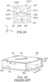
- Patent Document 1 JP 2008-193204 A discloses an antenna device provided with an antenna element formed of a sheet metal. It is said that the antenna device of Patent Document 1 can be downsized in comparison with a flat surface type antenna device provided with a ceramic substrate.
- an antenna device 90 disclosed in Patent Document 1 is provided with a dielectric substrate 92, an antenna element 95 which is formed of a sheet metal and arranged at a predetermined interval from the dielectric substrate 92, a plurality of leg pieces 952 extending from the antenna element 95 toward the dielectric substrate 92, a chip capacitor 94 electrically connected to the leg pieces 952 and the dielectric substrate 92, and an insertion member 96 which is made of resin and inserted between the dielectric substrate 92 and the antenna element 95.
- an object of the present invention to provide an antenna device which is small and capable of dual-band communication and to provide an antenna element used in the antenna device.
- the object is achived by the antenna element as defined by claim 1 and the amtenna device as defined by claim 6.
- each of the first lower conductor and the second lower conductor forms a capacitor together with the upper conductor.
- the antenna element can be downsized.
- the antenna device provided with the antenna element can also be downsized.
- a shape of the second lower conductor and a size of the second lower conductor influence setting of two frequencies of first and second resonances
- a shape of the first lower conductor and a size of the first lower conductor only influence setting of the frequency of the first resonance. Accordingly, by deciding the shape and the size of each of the first lower conductor and the second lower conductor, the first resonance and the second resonance can be set to desired frequencies.
- the antenna element for the antenna device which is capable of dual-band communication can be obtained
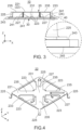
- an antenna device 10 is provided with an antenna element 20, a dielectric substrate 30 and a ground conductor 40.
- the antenna element 20 is provided on the ground conductor 40 via the dielectric substrate (or a dielectric body) 30 and thereby forms the antenna device 10.
- the antenna element 20 has an upper element 22 and a lower element 24.
- the upper element 22 is located upward of the lower element 24.
- the up-down direction is a Z-direction. A positive Z-direction is directed upward while a negative Z-direction is directed downward.
- the upper element 22 is provided with an upper conductor 221, at least one first leg portion 223, at least one second leg portion 225 and at least one feeding portion 227.
- the lower element 24 is provided with at least one first lower conductor 241 and at least one second lower conductor 243.
- the upper element 22 is formed of a single sheet metal.
- the upper conductor 221, the at least one first leg portion 223, the at least one second leg portion 225 and the at least one feeding portion 227 are formed of a single sheet metal.
- the upper element 22 is integrally formed by punching out a single sheet metal, followed by bending the punched-out sheet metal.
- the upper element 22 may be formed by use of a plurality of sheet metals.
- the upper element 22 may be formed by a laser direct structuring (LDS) method.
- LDS laser direct structuring
- each of the at least one first leg portion 223 and the at least one second leg portion 225 is four in number.
- the at least one feeding portion 227 is two in number.
- the at least one feeding portion 227 has two feeding portions 227.
- the present invention is not limited thereto.
- Each of the number of the first leg portions 223, the number of the second leg portions 225 and the number of the feeding portions 227 may be freely set.
- the lower element 24 is provided with the first lower conductors 241 and the second lower conductors 243.
- the first lower conductors 241 and the second lower conductors 243 are provided on an upper surface of the dielectric substrate 30.
- the first lower conductors 241 and the second lower conductors 243 may be formed by etching a conductor layer formed on the upper surface of the dielectric substrate 30.
- the first lower conductors 241 and the second lower conductors 243 may be formed by sticking conductor sheets or films each of which has a predetermined shape on the upper surface of the dielectric substrate 30.
- the present invention is not limited thereto.
- At least part of the lower element 24 may be integrally formed with the upper element 22 by using a material same as that of the upper element 22.
- the first lower conductors 241 and the second lower conductors 243 may not be located on the same plane perpendicular to the up-down direction. In other words, the first lower conductors 241 and the second lower conductors 243 may be located at different positions in the up-down direction. In that case, each of the first lower conductors 241 may overlap with any of the second lower conductors 243 in plan view. However, the first lower conductors 241 must be electrically separated from the second lower conductors 243.
- the first lower conductors 241 correspond to the first leg portions 223, respectively.
- the at least one first lower conductor 241 and the at least one first leg portion 223 are the same as each other in number.
- the at least one first lower conductor 241 is four in number.
- the at least one first lower conductor 241 has four first lower conductors 241.
- the second lower conductors 243 correspond to the second leg portions 225, respectively.
- the at least one second lower conductor 243 and the at least one second leg portion 225 are the same as each other in number.
- the at least one second lower conductor 243 is four in number.
- the at least one second lower conductor 243 has four second lower conductors 243.
- the number of the first lower conductors 241 may be freely set, provided that it is equal to the number of the first leg portions 223.
- the number of the second lower conductors 243 may be freely set, provided that it is equal to the number of the second leg portions 225.
- At least one feeding pad 32 is further provided on the upper surface of the dielectric substrate 30, on the upper surface of the dielectric substrate 30, at least one feeding pad 32 is further provided.
- the feeding pads 32 correspond to the feeding portions 227, respectively.
- the at least one feeding pad 32 is two in number.
- the feeding pads 32 are connected to feeding lines (not shown) provided on a lower surface of the dielectric substrate 30 through vias piercing through the dielectric substrate 30 in the up-down direction.
- the ground conductor 40 is located just under the dielectric substrate 30.
- the antenna device 10 is mounted on the ground conductor 40.
- the ground conductor 40 a circuit board in which a conductor layer is formed on an entire surface of each of upper and lower surfaces of a dielectric substrate may be used. In that case, it is preferable that the conductor layer on the upper surface and the conductor layer on the lower surface are connected to each other by use of vias or the like.
- a ground layer 245 is formed on the lower surface of the dielectric substrate 30 and covers almost the whole of the lower surface of the dielectric substrate 30.
- the ground conductor 40 arranged under the dielectric substrate 30 is electrically connected to the ground layer 245.
- the present invention is not limited thereto.
- the dielectric substrate 30 may not have the ground layer 245.
- an outer shape of the upper conductor 221 is generally square in plan view.
- the outer shape of the upper conductor 221 may not be generally square in plan view. Nevertheless, in order to use the antenna device 10 for communication using circular polarized waves, it is preferable that the outer shape of the upper conductor 221 has approximately n-fold symmetry in plan view.
- n is a multiple of four (the same applies hereafter).
- the upper conductor 221 has a middle portion 231, a ring portion 233 and coupling portions 235.
- the middle portion 231 is part of the upper conductor 221 which includes a middle of the upper conductor 221 in plan view.
- the ring portion 233 is part of the upper conductor 221 which is along an outer edge of the upper conductor 221.
- the coupling portions 235 are parts of the upper conductor 221 each of which couples the middle portion 231 and the ring portion 233 to each other. It is noted that a boundary between the middle portion 231 and each of the coupling portions 235 and a boundary between the ring portion 233 and each of the coupling portions 235 are indefinite.
- an outer shape of the middle portion 231 is square approximately analogous to the outer shape of the upper conductor 221 in plan view.
- the ring portion 233 has a frame shape which is generally square that is along the outer shape of the upper conductor 221.
- the ring portion 233 is located apart from and outward of the middle portion 231 and continuously surrounds the middle portion 231 in plan view.
- the coupling portions 235 are four in number.
- the coupling portions 235 correspond to four corners of the middle portion 231, respectively, and to four corners of the ring portion 233, respectively.
- Each of the coupling portions 235 couples the corner of the middle portion 231 corresponding thereto to the corner of the ring portion 233 corresponding thereto.
- the middle portion 231, the ring portion 233 and the coupling portions 235 are located on a plane intersecting with the up-down direction.
- the upper conductor 221 extends in the plane intersecting with the up-down direction.
- the upper conductor 221 extends in a plane perpendicular to the up-down direction.
- the ring portion 233 may not be, in part, located on the plane on which the middle portion 231 and the coupling portions 235 are located.
- the first leg portions 223 extend from the middle portion 231.
- the first leg portions 223 extend outward in plan view.
- each of the first leg portions 223 extends outward from any one of four edges of the middle portion 231 in a horizontal direction, then extends downward and further extends outward in the horizontal direction.
- each of the first leg portions 223 extends in either a front-rear direction or a lateral direction.
- the front-rear direction is an X-direction
- the lateral direction is a Y-direction. A positive X-direction is directed forward while a negative X-direction is directed rearward.
- the second leg portions 225 extend from the ring portion 233.
- the second leg portions 225 extend outward from an outer edge of the ring portion 233 in plan view.
- each of the second leg portions 225 extends outward from any one of four corners of the ring portion 233 in the horizontal direction, then extends diagonally downward and further extends outward in the horizontal direction.
- a direction in which each of the second leg portions 225 extends is an outward direction in a diagonal direction of the upper conductor 221.
- the second leg portions 225 may extend inward from inner edges of the ring portion 233 in plan view. In that case, the second leg portions 225 may extend inward or outward of the ring portion 233 in plan view.
- the feeding portions 227 extend from the upper conductor 221.
- the feeding portions 227 respectively extend from two of the coupling portions 235 adjacent to each other in the front-rear direction.
- the feeding portions 227 may extend from the middle portion 231.
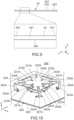
- the first lower conductors 241 are apart from each other and arranged on the middle portion 231 of the dielectric substrate 30.
- the first lower conductors 241 are arranged in four-fold symmetry about the middle of the dielectric substrate 30 in plan view.
- a shape of each of the first lower conductors 241 is an enneagon which has line symmetry about a straight line.
- the present invention is not limited thereto.
- the shape of each of the first lower conductors 241 may be freely set. Nevertheless, it is preferable that the first lower conductors 241 are formed in approximately n-fold symmetry about the middle of the dielectric substrate 30 in plan view.
- each of the first lower conductors 241 is connected to the first leg portion 223 corresponding thereto.
- the first lower conductors 241 are connected to the first leg portions 223 in a one-to-one relationship. Owing to existence of the first leg portions 223, the first lower conductors 241 are apart from the upper conductor 221 in the up-down direction.
- the second lower conductors 243 are arranged at corner portions of the dielectric substrate 30, respectively.
- Each of the second lower conductors 243 is distinct and separated from the first lower conductors 241 and apart from all of the first lower conductors 241.
- a shape of each of the second lower conductors 243 is square in plan view.
- the shape of each of the second lower conductors 243 may be freely set. Nevertheless, it is preferable that the second lower conductors 243 are formed in approximately n-fold symmetry about the middle of the dielectric substrate 30 in plan view.
- each of the second lower conductors 243 is connected to the second leg portion 225 corresponding thereto.
- the second lower conductors 243 are connected to the second leg portions 225 in a one-to-one relationship. Owing to existence of the second leg portions 225, the second lower conductors 243 are apart from the upper conductor 221 in the up-down direction.
- each of the feeding pads 32 is arranged on a diagonal line of the dielectric substrate 30.
- Each of the feeding pads 32 is located between two of the first lower conductors 241 adjacent to each other.
- the two feeding pads 32 are located on a straight line along the front-rear direction and sandwich one of the first lower conductors 241.
- each of the first lower conductors 241 and the second lower conductors 243 forms a capacitor together with the upper conductor 221. Accordingly, existence of the first lower conductors 241 and the second lower conductors 243 affects resonant frequencies of the antenna device 10. In detail, the existence of the first lower conductors 241 and the second lower conductors 243 reduces the resonant frequencies in comparison with a case of their absence. In other words, the existence of the first lower conductors 241 and the second lower conductors 243 allows the antenna element 20 having predetermined resonance frequencies to be downsized and thereby allows the antenna device 10 to be downsized.
- each of the first lower conductors 241 and the second lower conductors 243 also forms a capacitor together with the ground conductor 40.
- a capacitor element such as a chip capacitor, may be connected between the ground conductor 40 and each of the first lower conductors 241 and the second lower conductors 243.
- the antenna device 10 shown in Figs. 1 to 3 has a first resonance frequency and a second resonance frequency higher than the first resonance frequency.
- the shape of the second lower conductor 243 and a size of the second lower conductor 243 affect setting of both the first resonance frequency and the second resonance frequency.
- the shape of the first lower conductor 241 and a size of the first lower conductor 241 only affect setting of the first resonance frequency. Accordingly, decision of the shape and the size of each of the first lower conductors 241 and the second lower conductors 243 makes it possible to set each of the first resonance frequency and the second resonance frequency to a desired frequency.
- the antenna element 20 and the antenna device 10 each of which is capable of dual-band communication can be obtained.
- the antenna device 10 shown in Figs. 1 to 3 adopts the two-point feeding system.
- the antenna element 20 can perform communication using circular polarized waves each of which has a high degree of roundness.
- the outer shape of the upper conductor 221, an arrangement of the first lower conductors 241 and an arrangement of the second lower conductors 243 are preferable to have approximately n-fold symmetry.
- an antenna device 10A according to a second embodiment of the present invention is provided with an antenna element 20A, a dielectric substrate 30A and a ground conductor 40A.
- the antenna device 10A is basically formed in a manner similar to the antenna device 10 according to the first embodiment of the present invention.
- the antenna element 20A is provided with an upper conductor 221A, at least one first leg portion 223A, at least one second leg portion 225A, at least one feeding portion 227A, at least one first lower conductor 241A and at least one second lower conductor 243A.
- the antenna element 20A is formed of a single sheet metal.
- the upper conductor 221A has a middle portion 231A, a ring portion 233A and coupling portions 235A as with the upper conductor 221 of the first embodiment.
- each of the at least one first leg portion 223A, the at least one second leg portion 225A, the at least one first lower conductor 241A and the at least one second lower conductor 243A is four in number.
- the at least one feeding portion 227A is two in number.
- the antenna element 20A is mounted on an upper surface of the dielectric substrate 30A.
- a ground conductor 40A is provided on a lower surface of the dielectric substrate 30A.
- the antenna element 20A can be downsized, and the antenna device 10A can be downsized. Moreover, according to the present embodiment, the antenna element 20A and the antenna device 10A each of which is capable of dual-band communication can be obtained. Because the first lower conductors 241A and the second lower conductors 243A are united to the antenna element 20A, deterioration of positional accuracy of the first lower conductors 241A and the second lower conductors 243A, which depends on attaching accuracy, with respect to the upper conductor 221 can be prevented.
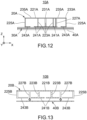
- an antenna element 20B is provided with an upper conductor 221B, at least one first lower conductor 241B, at least one second lower conductor 243B, at least one first leg portion 223B, at least one second leg portion 225B and at least one feeding portion 227B.
- the antenna element 20B is arranged apart from and upward of a ground conductor 40B and forms an antenna device 10B.
- the antenna element 20B and the ground conductor 40B are fixed to each other with supporting members (not shown).
- air exists as a dielectric body.
- the dielectric body may be air.
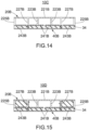
- an antenna device 10C is formed by arranging an antenna element 20B to be apart from and upward of a ground conductor 40B. In the up-down direction, a space between the ground conductor 40B and each of first lower conductors 241B and second lower conductors 243B is filled with a dielectric body 34.
- a dielectric body 34 any resin, such as epoxy resin, Teflon (Registered Trademark), etc., may be used.
- the dielectric body may not be a rigid substrate.
- an antenna device 10D is formed by arranging an antenna element 20B to be apart from and upward of a ground conductor 40B. In the up-down direction, a space between an upper conductor 221B of the antenna element 20B and the ground conductor 40B is filled with a dielectric body 34.
- a dielectric body 34 any resin, such as epoxy resin, Teflon (Registered Trademark), etc., may be used.
- the antenna device of the present invention not only a space between the antenna element 20B and the ground conductor 40B but also a space inside the antenna element 20B may be filled with a dielectric body.
- an antenna device 10E is formed by arranging an antenna element 20B to be apart from and upward of a ground conductor 40B.
- a space between an upper conductor 221B of the antenna element 20B and each of first lower conductors 241B and second lower conductors 243B is filled with a dielectric body 34.
- air exists as a dielectric body.
- only the space inside the antenna element 20B may be filled with a tangible dielectric body.
- the upper element 22 or the antenna element 20A is formed of a single sheet metal, cutting and rising the first leg portions 223 or 223A and the feeding portions 227 or 228A are carried out. At that time, in the upper conductor 221 or 221A, slots or aperture portions are inevitably formed.
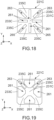
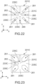
- a shape of each of the slots may be freely set as shown in any of Figs. 17 to 24 , for example. Nevertheless, it is preferable that the shape of the upper conductor, shapes of the slots and arrangement of the slots have n-fold symmetry in order to realize the communication using circular polarized waves.
- first slots 261 and two second slots 263 are formed in an upper conductor 221C.
- a shape of each of the first slots 261 and the second slots 263 is rectangular.
- the first slots 261 correspond to the first leg portions 223 of the first embodiment, respectively, for example.
- the second slots 263 correspond to the feeding portions 227 of the first embodiment, respectively, for example.
- the third slots 265 are further formed in comparison with the upper conductor 221C of Fig. 17 .
- the third slots 265 are dummy slots which correspond to neither the first leg portions 223 nor the feeding portions 227.
- the shape of the upper conductor 221 of Fig. 18 has four-fold symmetry. With this structure, circular polarized waves each of which has a higher degree of roundness are obtained.
- a shape of each of the first slots 261 may be hexagonal.
- each of the first slots 261 is arranged between a middle of the upper conductor 221C and any one of edges of the upper conductor 221C
- each of the second slots 263 is arranged between the middle of the upper conductor 221C and any one of corners of the upper conductor 221C.
- each of the first slots 261 may be arranged between the middle of the upper conductor 221C and any one of the corners of the upper conductor 221C
- each of the second slots 263 may be arranged between the middle of the upper conductor 221C and any one of the edges of the upper conductor 221C.
- a shape of each of the first slots 261 may be octagonal.
- the upper conductor 221C shown in each of Figs. 17 to 24 has a middle portion 231C, a ring portion 233c continuously surrounding the middle portion 231C and coupling portions 235C each of which couples the middle portion 231C and the ring portion 233C to each other.
Landscapes
- Details Of Aerials (AREA)
- Waveguide Aerials (AREA)
Claims (6)
- Antennenelement (20, 20A, 20B) zum Bilden einer Antennenvorrichtung (10, 10A-E) durch Anbringen an einem Masseleiter (40, 40A, 40B) über einen dielektrischen Körper (34), wobei:das Antennenelement (20, 20A, 20B) einen oberen Leiter (221, 221A-C), mindestens einen ersten unteren Leiter (241, 241A, 241B), mindestens einen zweiten unteren Leiter (243, 243A, 243B), mindestens einen ersten Schenkelabschnitt (223, 223A, 223B), mindestens einen zweiten Schenkelabschnitt (225, 225A, 225B) und mindestens einen Zuführungsabschnitt (227, 227A, 227B) umfasst;der obere Leiter (221, 221A-C) einen Mittelabschnitt (231, 231A, 231C), einen Ringabschnitt (233, 233A, 233C) und einen Koppelabschnitt (235, 235A, 235C) aufweist;der Ringabschnitt (233, 233A, 233C) beabstandet von dem Mittelabschnitt (231, 231A, 231C) angeordnet ist und den Mittelabschnitt (231, 231A, 231C) kontinuierlich umgibt;der Koppelabschnitt (235, 235A, 235C) den Mittelabschnitt (231, 231A, 231C) und den Ringabschnitt (233, 233A, 233C) miteinander koppelt;der mindestens eine erste Schenkelabschnitt (223, 223A, 223B) sich von dem Mittelabschnitt (231, 231A, 231C) aus erstreckt;der mindestens eine zweite Schenkelabschnitt (225, 225A, 225B) sich von dem Ringabschnitt (233, 233A, 233C) aus erstreckt;der mindestens eine erste untere Leiter (241, 241A, 241B) von dem oberen Leiter (221, 221A-C) in einer Auf-Ab-Richtung beabstandet ist und an den mindestens einen ersten Schenkelabschnitt (223, 223A, 223B) angeschlossen ist;der mindestens eine zweite untere Leiter (243, 243A, 243B) von dem mindestens einen ersten unteren Leiter (241, 241A, 241B) verschieden und getrennt ist und von dem mindestens einen ersten unteren Leiter (241, 241A, 241B) beabstandet ist;der mindestens eine zweite untere Leiter (243, 243A, 243B) von dem oberen Leiter (221, 221A-C) in der Auf-Ab-Richtung beabstandet ist und an den mindestens einen zweiten Schenkelabschnitt (225, 225A, 225B) angeschlossen ist;der mindestens eine Zuführungsabschnitt (227, 227A, 227B) sich von dem oberen Leiter (221, 221A-C) aus erstreckt;der mindestens eine erste untere Leiter (241, 241A, 241B) und der mindestens eine erste Schenkelabschnitt (223, 223A, 223B) in ihrer Anzahl gleich sind und in einer Eins-zu-Eins-Beziehung aneinander angeschlossen sind; undder mindestens eine zweite untere Leiter (243, 243A, 243B) und der mindestens eine zweite Schenkelabschnitt (225, 225A, 225B) in ihrer Anzahl gleich sind und in einer Eins-zu-Eins-Beziehung aneinander angeschlossen sind,der mindestens eine erste untere Leiter und der mindestens eine zweite untere Leiter so konfiguriert sind, dass sie jeweils kapazitiv an einen Masseleiter (40) angeschlossen sind.
- Antennenelement (20, 20A, 20B) nach Anspruch 1, wobei:der mindestens eine Zuführungsabschnitt (227, 227A, 227B) zwei Zuführungsabschnitte umfasst; undzwei imaginäre Linien, von denen jede eine Mitte des Mittelabschnitts (231, 231A, 231C) und jeden der zwei Zuführungsabschnitte miteinander verbindet, einander in einer Draufsicht um 90 Grad schneiden.
- Antennenelement (20, 20A, 20B) nach Anspruch 1 oder 2, wobei:der mindestens eine erste untere Leiter (241, 241A, 241B) vier erste untere Leiter umfasst; undder mindestens eine zweite untere Leiter (243, 243A, 243B) vier zweite untere Leiter umfasst.
- Antennenelement (20, 20A, 20B) nach einem der Ansprüche 1 bis 3, wobei:der obere Leiter (221, 221A-C) sich in einer Ebene erstreckt, die die Auf-Ab-Richtung schneidet; undder obere Leiter (221, 221A-C), der mindestens eine erste Schenkelabschnitt (223, 223A, 223B), der mindestens eine zweite Schenkelabschnitt (225, 225A, 225B) und der mindestens eine Zuführungsabschnitt (227, 227A, 227B) aus einem einzigen Metallblech gebildet sind.
- Antennenelement (20A, 20B) nach einem der Ansprüche 1 bis 3, wobei:der obere Leiter (221A-C) sich in einer Ebene erstreckt, die die Auf-Ab-Richtung schneidet; undder obere Leiter (221A-C), der mindestens eine erste untere Leiter (241A, 241B), der mindestens eine zweite untere Leiter (243A, 243B), der mindestens eine erste Schenkelabschnitt (223A, 223B), der mindestens eine zweite Schenkelabschnitt (225A, 225B) und der mindestens eine Zuführungsabschnitt (227A, 227B) aus einem einzigen Metallblech gebildet sind.
- Antennenvorrichtung (10C, 10D), umfassendein Antennenelement (20, 20A, 20B) nach einem der Ansprüche 1 bis 5,einen Masseleiter (40, 40A, 40B) undeinen dielektrischen Körper (34), der zwischen dem Antennenelement (20, 20A, 20B) und dem Masseleiter (40, 40A, 40B) liegt.
Applications Claiming Priority (2)
| Application Number | Priority Date | Filing Date | Title |
|---|---|---|---|
| JP2022164177A JP2024057437A (ja) | 2022-10-12 | 2022-10-12 | アンテナエレメント及びアンテナ装置 |
| JP2022164174A JP2024057435A (ja) | 2022-10-12 | 2022-10-12 | アンテナエレメント及びアンテナ装置 |
Publications (2)
| Publication Number | Publication Date |
|---|---|
| EP4354656A1 EP4354656A1 (de) | 2024-04-17 |
| EP4354656B1 true EP4354656B1 (de) | 2025-05-07 |
Family
ID=87863267
Family Applications (2)
| Application Number | Title | Priority Date | Filing Date |
|---|---|---|---|
| EP23194364.8A Pending EP4354660A1 (de) | 2022-10-12 | 2023-08-30 | Antennenelement und antennenvorrichtung |
| EP23194361.4A Active EP4354656B1 (de) | 2022-10-12 | 2023-08-30 | Antennenelement und antennenvorrichtung |
Family Applications Before (1)
| Application Number | Title | Priority Date | Filing Date |
|---|---|---|---|
| EP23194364.8A Pending EP4354660A1 (de) | 2022-10-12 | 2023-08-30 | Antennenelement und antennenvorrichtung |
Country Status (3)
| Country | Link |
|---|---|
| US (2) | US12482948B2 (de) |
| EP (2) | EP4354660A1 (de) |
| TW (2) | TWI875171B (de) |
Cited By (1)
| Publication number | Priority date | Publication date | Assignee | Title |
|---|---|---|---|---|
| EP4471986B1 (de) * | 2023-05-31 | 2026-03-25 | Japan Aviation Electronics Industry, Limited | Antennenelement und antennenvorrichtung - ep |
Family Cites Families (17)
| Publication number | Priority date | Publication date | Assignee | Title |
|---|---|---|---|---|
| JP4229418B2 (ja) | 2000-06-21 | 2009-02-25 | Tdk株式会社 | 円偏波パッチアンテナ |
| JP3896331B2 (ja) | 2003-01-15 | 2007-03-22 | Fdk株式会社 | 円偏波パッチアンテナ |
| JP3814271B2 (ja) | 2003-11-10 | 2006-08-23 | アルプス電気株式会社 | アンテナ装置 |
| KR101129997B1 (ko) * | 2006-08-24 | 2012-03-26 | 야기안테나 가부시기가이샤 | 안테나 장치 |
| JP2008079009A (ja) | 2006-09-21 | 2008-04-03 | Mitsumi Electric Co Ltd | アンテナ装置 |
| JP4404225B2 (ja) | 2007-07-12 | 2010-01-27 | ミツミ電機株式会社 | アンテナ装置 |
| JP2008079011A (ja) | 2006-09-21 | 2008-04-03 | Mitsumi Electric Co Ltd | アンテナ装置 |
| JP4456588B2 (ja) * | 2006-09-29 | 2010-04-28 | アルプス電気株式会社 | アンテナ構造及びヘッドセット |
| JP4882771B2 (ja) | 2007-02-01 | 2012-02-22 | ミツミ電機株式会社 | アンテナ装置 |
| CN201845860U (zh) * | 2010-09-30 | 2011-05-25 | 寰波科技股份有限公司 | 高增益多极化天线阵列模块 |
| KR101128872B1 (ko) * | 2010-11-29 | 2012-03-26 | 고형석 | 원편파 안테나 |
| JP2015216577A (ja) * | 2014-05-13 | 2015-12-03 | 富士通株式会社 | アンテナ装置 |
| CN108511913B (zh) * | 2018-05-03 | 2022-09-30 | 京信通信技术(广州)有限公司 | 基站天线及其双极化天线振子 |
| US11158948B2 (en) * | 2019-03-20 | 2021-10-26 | Samsung Electro-Mechanics Co., Ltd. | Antenna apparatus |
| WO2020242783A2 (en) * | 2019-05-24 | 2020-12-03 | Commscope Technologies Llc | Wireless communication systems having patch-type antenna arrays therein that support large scan angle radiation |
| CN112467343B (zh) * | 2019-09-09 | 2023-07-04 | 普罗斯通信技术(苏州)有限公司 | 一种高增益小型化天线振子及天线 |
| CN211670319U (zh) * | 2020-04-24 | 2020-10-13 | 瑞典爱立信有限公司 | 天线元件及包括该天线元件的基站天线 |
-
2023
- 2023-08-30 EP EP23194364.8A patent/EP4354660A1/de active Pending
- 2023-08-30 EP EP23194361.4A patent/EP4354656B1/de active Active
- 2023-09-01 US US18/241,249 patent/US12482948B2/en active Active
- 2023-09-01 US US18/241,247 patent/US12362493B2/en active Active
- 2023-09-04 TW TW112133456A patent/TWI875171B/zh active
- 2023-09-04 TW TW112133455A patent/TWI886561B/zh active
Cited By (2)
| Publication number | Priority date | Publication date | Assignee | Title |
|---|---|---|---|---|
| EP4471986B1 (de) * | 2023-05-31 | 2026-03-25 | Japan Aviation Electronics Industry, Limited | Antennenelement und antennenvorrichtung - ep |
| US12609443B2 (en) | 2023-05-31 | 2026-04-21 | Japan Aviation Electronics Industry, Limited | Antenna element and antenna device |
Also Published As
| Publication number | Publication date |
|---|---|
| EP4354656A1 (de) | 2024-04-17 |
| TWI886561B (zh) | 2025-06-11 |
| US20240128649A1 (en) | 2024-04-18 |
| EP4354660A1 (de) | 2024-04-17 |
| US12362493B2 (en) | 2025-07-15 |
| TWI875171B (zh) | 2025-03-01 |
| US12482948B2 (en) | 2025-11-25 |
| US20240128648A1 (en) | 2024-04-18 |
| TW202418656A (zh) | 2024-05-01 |
| TW202418655A (zh) | 2024-05-01 |
Similar Documents
| Publication | Publication Date | Title |
|---|---|---|
| US11183766B2 (en) | Antenna module and electronic device | |
| JP4423809B2 (ja) | 複共振アンテナ | |
| US9112262B2 (en) | Planar array feed for satellite communications | |
| US10535921B2 (en) | Reconfigurable multi-band antenna with four to ten ports | |
| CN111129712B (zh) | 5g毫米波双极化天线模组及手持设备 | |
| WO2021082988A1 (zh) | 天线模组及电子设备 | |
| EP3698433A1 (de) | Resonatorgestützte patch-antenne | |
| CN111129713B (zh) | 一种5g毫米波双极化天线模组及终端设备 | |
| CN110350289B (zh) | 基于基片集成波导四分之一模馈电的低剖面有源微带天线 | |
| CN113036403B (zh) | 电子装置及其天线结构 | |
| CN112542682B (zh) | 一种去耦双极化低频振子及嵌入式双频段阵列天线 | |
| US9728845B2 (en) | Dual antenna structure having circular polarisation characteristics | |
| CN109462028B (zh) | 一种射频微机电微带天线 | |
| WO2022105999A1 (en) | A low profile device comprising layers of coupled resonance structures | |
| EP4354656B1 (de) | Antennenelement und antennenvorrichtung | |
| WO2007072710A1 (ja) | 指向性可変アンテナ | |
| CN221486824U (zh) | 天线及天线装置 | |
| WO2025180427A1 (en) | Dual-polarized dielectric dipole antenna | |
| US8604983B2 (en) | CRLH antenna structures | |
| CN219534865U (zh) | 一种双频毫米波天线模组及电子设备 | |
| CN112635981B (zh) | 天线组件、天线阵列和通信设备 | |
| CN117525899A (zh) | 一种双频段5g微带天线 | |
| WO2024165151A1 (en) | Antenna, mobile communication base station and user device | |
| US20260039010A1 (en) | Radiating elements for multiband base station antennas having cavity phase shifters and related linear array assemblies and base station antennas | |
| US20260018793A1 (en) | Ultra-dense triband unit cell |
Legal Events
| Date | Code | Title | Description |
|---|---|---|---|
| PUAI | Public reference made under article 153(3) epc to a published international application that has entered the european phase |
Free format text: ORIGINAL CODE: 0009012 |
|
| STAA | Information on the status of an ep patent application or granted ep patent |
Free format text: STATUS: THE APPLICATION HAS BEEN PUBLISHED |
|
| AK | Designated contracting states |
Kind code of ref document: A1 Designated state(s): AL AT BE BG CH CY CZ DE DK EE ES FI FR GB GR HR HU IE IS IT LI LT LU LV MC ME MK MT NL NO PL PT RO RS SE SI SK SM TR |
|
| STAA | Information on the status of an ep patent application or granted ep patent |
Free format text: STATUS: REQUEST FOR EXAMINATION WAS MADE |
|
| 17P | Request for examination filed |
Effective date: 20240830 |
|
| RBV | Designated contracting states (corrected) |
Designated state(s): AL AT BE BG CH CY CZ DE DK EE ES FI FR GB GR HR HU IE IS IT LI LT LU LV MC ME MK MT NL NO PL PT RO RS SE SI SK SM TR |
|
| RAP3 | Party data changed (applicant data changed or rights of an application transferred) |
Owner name: JAPAN AVIATION ELECTRONICS INDUSTRY, LIMITED |
|
| GRAP | Despatch of communication of intention to grant a patent |
Free format text: ORIGINAL CODE: EPIDOSNIGR1 |
|
| STAA | Information on the status of an ep patent application or granted ep patent |
Free format text: STATUS: GRANT OF PATENT IS INTENDED |
|
| INTG | Intention to grant announced |
Effective date: 20241202 |
|
| GRAS | Grant fee paid |
Free format text: ORIGINAL CODE: EPIDOSNIGR3 |
|
| GRAA | (expected) grant |
Free format text: ORIGINAL CODE: 0009210 |
|
| STAA | Information on the status of an ep patent application or granted ep patent |
Free format text: STATUS: THE PATENT HAS BEEN GRANTED |
|
| AK | Designated contracting states |
Kind code of ref document: B1 Designated state(s): AL AT BE BG CH CY CZ DE DK EE ES FI FR GB GR HR HU IE IS IT LI LT LU LV MC ME MK MT NL NO PL PT RO RS SE SI SK SM TR |
|
| REG | Reference to a national code |
Ref country code: GB Ref legal event code: FG4D |
|
| REG | Reference to a national code |
Ref country code: CH Ref legal event code: EP |
|
| REG | Reference to a national code |
Ref country code: DE Ref legal event code: R096 Ref document number: 602023003334 Country of ref document: DE |
|
| REG | Reference to a national code |
Ref country code: IE Ref legal event code: FG4D |
|
| REG | Reference to a national code |
Ref country code: NL Ref legal event code: MP Effective date: 20250507 |
|
| PG25 | Lapsed in a contracting state [announced via postgrant information from national office to epo] |
Ref country code: PT Free format text: LAPSE BECAUSE OF FAILURE TO SUBMIT A TRANSLATION OF THE DESCRIPTION OR TO PAY THE FEE WITHIN THE PRESCRIBED TIME-LIMIT Effective date: 20250908 Ref country code: FI Free format text: LAPSE BECAUSE OF FAILURE TO SUBMIT A TRANSLATION OF THE DESCRIPTION OR TO PAY THE FEE WITHIN THE PRESCRIBED TIME-LIMIT Effective date: 20250507 Ref country code: ES Free format text: LAPSE BECAUSE OF FAILURE TO SUBMIT A TRANSLATION OF THE DESCRIPTION OR TO PAY THE FEE WITHIN THE PRESCRIBED TIME-LIMIT Effective date: 20250507 |
|
| PGFP | Annual fee paid to national office [announced via postgrant information from national office to epo] |
Ref country code: DE Payment date: 20250827 Year of fee payment: 3 |
|
| REG | Reference to a national code |
Ref country code: LT Ref legal event code: MG9D |
|
| PG25 | Lapsed in a contracting state [announced via postgrant information from national office to epo] |
Ref country code: NO Free format text: LAPSE BECAUSE OF FAILURE TO SUBMIT A TRANSLATION OF THE DESCRIPTION OR TO PAY THE FEE WITHIN THE PRESCRIBED TIME-LIMIT Effective date: 20250807 Ref country code: GR Free format text: LAPSE BECAUSE OF FAILURE TO SUBMIT A TRANSLATION OF THE DESCRIPTION OR TO PAY THE FEE WITHIN THE PRESCRIBED TIME-LIMIT Effective date: 20250808 |
|
| PG25 | Lapsed in a contracting state [announced via postgrant information from national office to epo] |
Ref country code: NL Free format text: LAPSE BECAUSE OF FAILURE TO SUBMIT A TRANSLATION OF THE DESCRIPTION OR TO PAY THE FEE WITHIN THE PRESCRIBED TIME-LIMIT Effective date: 20250507 Ref country code: PL Free format text: LAPSE BECAUSE OF FAILURE TO SUBMIT A TRANSLATION OF THE DESCRIPTION OR TO PAY THE FEE WITHIN THE PRESCRIBED TIME-LIMIT Effective date: 20250507 |
|
| REG | Reference to a national code |
Ref country code: AT Ref legal event code: MK05 Ref document number: 1793550 Country of ref document: AT Kind code of ref document: T Effective date: 20250507 |
|
| PG25 | Lapsed in a contracting state [announced via postgrant information from national office to epo] |
Ref country code: BG Free format text: LAPSE BECAUSE OF FAILURE TO SUBMIT A TRANSLATION OF THE DESCRIPTION OR TO PAY THE FEE WITHIN THE PRESCRIBED TIME-LIMIT Effective date: 20250507 |
|
| PG25 | Lapsed in a contracting state [announced via postgrant information from national office to epo] |
Ref country code: HR Free format text: LAPSE BECAUSE OF FAILURE TO SUBMIT A TRANSLATION OF THE DESCRIPTION OR TO PAY THE FEE WITHIN THE PRESCRIBED TIME-LIMIT Effective date: 20250507 |
|
| PG25 | Lapsed in a contracting state [announced via postgrant information from national office to epo] |
Ref country code: AT Free format text: LAPSE BECAUSE OF FAILURE TO SUBMIT A TRANSLATION OF THE DESCRIPTION OR TO PAY THE FEE WITHIN THE PRESCRIBED TIME-LIMIT Effective date: 20250507 |
|
| PGFP | Annual fee paid to national office [announced via postgrant information from national office to epo] |
Ref country code: FR Payment date: 20250814 Year of fee payment: 3 |
|
| PG25 | Lapsed in a contracting state [announced via postgrant information from national office to epo] |
Ref country code: RS Free format text: LAPSE BECAUSE OF FAILURE TO SUBMIT A TRANSLATION OF THE DESCRIPTION OR TO PAY THE FEE WITHIN THE PRESCRIBED TIME-LIMIT Effective date: 20250807 |
|
| PG25 | Lapsed in a contracting state [announced via postgrant information from national office to epo] |
Ref country code: IS Free format text: LAPSE BECAUSE OF FAILURE TO SUBMIT A TRANSLATION OF THE DESCRIPTION OR TO PAY THE FEE WITHIN THE PRESCRIBED TIME-LIMIT Effective date: 20250907 |
|
| PG25 | Lapsed in a contracting state [announced via postgrant information from national office to epo] |
Ref country code: LV Free format text: LAPSE BECAUSE OF FAILURE TO SUBMIT A TRANSLATION OF THE DESCRIPTION OR TO PAY THE FEE WITHIN THE PRESCRIBED TIME-LIMIT Effective date: 20250507 |
|
| PG25 | Lapsed in a contracting state [announced via postgrant information from national office to epo] |
Ref country code: SM Free format text: LAPSE BECAUSE OF FAILURE TO SUBMIT A TRANSLATION OF THE DESCRIPTION OR TO PAY THE FEE WITHIN THE PRESCRIBED TIME-LIMIT Effective date: 20250507 Ref country code: DK Free format text: LAPSE BECAUSE OF FAILURE TO SUBMIT A TRANSLATION OF THE DESCRIPTION OR TO PAY THE FEE WITHIN THE PRESCRIBED TIME-LIMIT Effective date: 20250507 |
|
| PG25 | Lapsed in a contracting state [announced via postgrant information from national office to epo] |
Ref country code: CZ Free format text: LAPSE BECAUSE OF FAILURE TO SUBMIT A TRANSLATION OF THE DESCRIPTION OR TO PAY THE FEE WITHIN THE PRESCRIBED TIME-LIMIT Effective date: 20250507 |
|
| PG25 | Lapsed in a contracting state [announced via postgrant information from national office to epo] |
Ref country code: EE Free format text: LAPSE BECAUSE OF FAILURE TO SUBMIT A TRANSLATION OF THE DESCRIPTION OR TO PAY THE FEE WITHIN THE PRESCRIBED TIME-LIMIT Effective date: 20250507 |
|
| PG25 | Lapsed in a contracting state [announced via postgrant information from national office to epo] |
Ref country code: SK Free format text: LAPSE BECAUSE OF FAILURE TO SUBMIT A TRANSLATION OF THE DESCRIPTION OR TO PAY THE FEE WITHIN THE PRESCRIBED TIME-LIMIT Effective date: 20250507 |
|
| PG25 | Lapsed in a contracting state [announced via postgrant information from national office to epo] |
Ref country code: IT Free format text: LAPSE BECAUSE OF FAILURE TO SUBMIT A TRANSLATION OF THE DESCRIPTION OR TO PAY THE FEE WITHIN THE PRESCRIBED TIME-LIMIT Effective date: 20250507 |
|
| REG | Reference to a national code |
Ref country code: DE Ref legal event code: R097 Ref document number: 602023003334 Country of ref document: DE |
|
| PG25 | Lapsed in a contracting state [announced via postgrant information from national office to epo] |
Ref country code: RO Free format text: LAPSE BECAUSE OF FAILURE TO SUBMIT A TRANSLATION OF THE DESCRIPTION OR TO PAY THE FEE WITHIN THE PRESCRIBED TIME-LIMIT Effective date: 20250507 |
|
| PLBE | No opposition filed within time limit |
Free format text: ORIGINAL CODE: 0009261 |
|
| STAA | Information on the status of an ep patent application or granted ep patent |
Free format text: STATUS: NO OPPOSITION FILED WITHIN TIME LIMIT |
|
| REG | Reference to a national code |
Ref country code: CH Ref legal event code: L10 Free format text: ST27 STATUS EVENT CODE: U-0-0-L10-L00 (AS PROVIDED BY THE NATIONAL OFFICE) Effective date: 20260318 |
|
| PG25 | Lapsed in a contracting state [announced via postgrant information from national office to epo] |
Ref country code: MC Free format text: LAPSE BECAUSE OF FAILURE TO SUBMIT A TRANSLATION OF THE DESCRIPTION OR TO PAY THE FEE WITHIN THE PRESCRIBED TIME-LIMIT Effective date: 20250507 |
|
| 26N | No opposition filed |
Effective date: 20260210 |
|
| PG25 | Lapsed in a contracting state [announced via postgrant information from national office to epo] |
Ref country code: LU Free format text: LAPSE BECAUSE OF NON-PAYMENT OF DUE FEES Effective date: 20250830 |