EP4350026A1 - Verfahren zur herstellung von siliciumbeschichtetem kupfer, siliciumbeschichtetes antioxidationskupfer damit und halbleiterbauelement damit - Google Patents
Verfahren zur herstellung von siliciumbeschichtetem kupfer, siliciumbeschichtetes antioxidationskupfer damit und halbleiterbauelement damit Download PDFInfo
- Publication number
- EP4350026A1 EP4350026A1 EP22811536.6A EP22811536A EP4350026A1 EP 4350026 A1 EP4350026 A1 EP 4350026A1 EP 22811536 A EP22811536 A EP 22811536A EP 4350026 A1 EP4350026 A1 EP 4350026A1
- Authority
- EP
- European Patent Office
- Prior art keywords
- silicon
- copper
- layer
- coated
- oxygen
- Prior art date
- Legal status (The legal status is an assumption and is not a legal conclusion. Google has not performed a legal analysis and makes no representation as to the accuracy of the status listed.)
- Pending
Links
Images



Classifications
-
- C—CHEMISTRY; METALLURGY
- C23—COATING METALLIC MATERIAL; COATING MATERIAL WITH METALLIC MATERIAL; CHEMICAL SURFACE TREATMENT; DIFFUSION TREATMENT OF METALLIC MATERIAL; COATING BY VACUUM EVAPORATION, BY SPUTTERING, BY ION IMPLANTATION OR BY CHEMICAL VAPOUR DEPOSITION, IN GENERAL; INHIBITING CORROSION OF METALLIC MATERIAL OR INCRUSTATION IN GENERAL
- C23C—COATING METALLIC MATERIAL; COATING MATERIAL WITH METALLIC MATERIAL; SURFACE TREATMENT OF METALLIC MATERIAL BY DIFFUSION INTO THE SURFACE, BY CHEMICAL CONVERSION OR SUBSTITUTION; COATING BY VACUUM EVAPORATION, BY SPUTTERING, BY ION IMPLANTATION OR BY CHEMICAL VAPOUR DEPOSITION, IN GENERAL
- C23C14/00—Coating by vacuum evaporation, by sputtering or by ion implantation of the coating forming material
- C23C14/06—Coating by vacuum evaporation, by sputtering or by ion implantation of the coating forming material characterised by the coating material
- C23C14/14—Metallic material, boron or silicon
- C23C14/16—Metallic material, boron or silicon on metallic substrates or on substrates of boron or silicon
- C23C14/165—Metallic material, boron or silicon on metallic substrates or on substrates of boron or silicon by cathodic sputtering
-
- C—CHEMISTRY; METALLURGY
- C23—COATING METALLIC MATERIAL; COATING MATERIAL WITH METALLIC MATERIAL; CHEMICAL SURFACE TREATMENT; DIFFUSION TREATMENT OF METALLIC MATERIAL; COATING BY VACUUM EVAPORATION, BY SPUTTERING, BY ION IMPLANTATION OR BY CHEMICAL VAPOUR DEPOSITION, IN GENERAL; INHIBITING CORROSION OF METALLIC MATERIAL OR INCRUSTATION IN GENERAL
- C23C—COATING METALLIC MATERIAL; COATING MATERIAL WITH METALLIC MATERIAL; SURFACE TREATMENT OF METALLIC MATERIAL BY DIFFUSION INTO THE SURFACE, BY CHEMICAL CONVERSION OR SUBSTITUTION; COATING BY VACUUM EVAPORATION, BY SPUTTERING, BY ION IMPLANTATION OR BY CHEMICAL VAPOUR DEPOSITION, IN GENERAL
- C23C14/00—Coating by vacuum evaporation, by sputtering or by ion implantation of the coating forming material
- C23C14/06—Coating by vacuum evaporation, by sputtering or by ion implantation of the coating forming material characterised by the coating material
-
- C—CHEMISTRY; METALLURGY
- C23—COATING METALLIC MATERIAL; COATING MATERIAL WITH METALLIC MATERIAL; CHEMICAL SURFACE TREATMENT; DIFFUSION TREATMENT OF METALLIC MATERIAL; COATING BY VACUUM EVAPORATION, BY SPUTTERING, BY ION IMPLANTATION OR BY CHEMICAL VAPOUR DEPOSITION, IN GENERAL; INHIBITING CORROSION OF METALLIC MATERIAL OR INCRUSTATION IN GENERAL
- C23C—COATING METALLIC MATERIAL; COATING MATERIAL WITH METALLIC MATERIAL; SURFACE TREATMENT OF METALLIC MATERIAL BY DIFFUSION INTO THE SURFACE, BY CHEMICAL CONVERSION OR SUBSTITUTION; COATING BY VACUUM EVAPORATION, BY SPUTTERING, BY ION IMPLANTATION OR BY CHEMICAL VAPOUR DEPOSITION, IN GENERAL
- C23C14/00—Coating by vacuum evaporation, by sputtering or by ion implantation of the coating forming material
- C23C14/0015—Coating by vacuum evaporation, by sputtering or by ion implantation of the coating forming material characterized by the colour of the layer
-
- C—CHEMISTRY; METALLURGY
- C23—COATING METALLIC MATERIAL; COATING MATERIAL WITH METALLIC MATERIAL; CHEMICAL SURFACE TREATMENT; DIFFUSION TREATMENT OF METALLIC MATERIAL; COATING BY VACUUM EVAPORATION, BY SPUTTERING, BY ION IMPLANTATION OR BY CHEMICAL VAPOUR DEPOSITION, IN GENERAL; INHIBITING CORROSION OF METALLIC MATERIAL OR INCRUSTATION IN GENERAL
- C23C—COATING METALLIC MATERIAL; COATING MATERIAL WITH METALLIC MATERIAL; SURFACE TREATMENT OF METALLIC MATERIAL BY DIFFUSION INTO THE SURFACE, BY CHEMICAL CONVERSION OR SUBSTITUTION; COATING BY VACUUM EVAPORATION, BY SPUTTERING, BY ION IMPLANTATION OR BY CHEMICAL VAPOUR DEPOSITION, IN GENERAL
- C23C14/00—Coating by vacuum evaporation, by sputtering or by ion implantation of the coating forming material
- C23C14/06—Coating by vacuum evaporation, by sputtering or by ion implantation of the coating forming material characterised by the coating material
- C23C14/08—Oxides
-
- C—CHEMISTRY; METALLURGY
- C23—COATING METALLIC MATERIAL; COATING MATERIAL WITH METALLIC MATERIAL; CHEMICAL SURFACE TREATMENT; DIFFUSION TREATMENT OF METALLIC MATERIAL; COATING BY VACUUM EVAPORATION, BY SPUTTERING, BY ION IMPLANTATION OR BY CHEMICAL VAPOUR DEPOSITION, IN GENERAL; INHIBITING CORROSION OF METALLIC MATERIAL OR INCRUSTATION IN GENERAL
- C23C—COATING METALLIC MATERIAL; COATING MATERIAL WITH METALLIC MATERIAL; SURFACE TREATMENT OF METALLIC MATERIAL BY DIFFUSION INTO THE SURFACE, BY CHEMICAL CONVERSION OR SUBSTITUTION; COATING BY VACUUM EVAPORATION, BY SPUTTERING, BY ION IMPLANTATION OR BY CHEMICAL VAPOUR DEPOSITION, IN GENERAL
- C23C14/00—Coating by vacuum evaporation, by sputtering or by ion implantation of the coating forming material
- C23C14/58—After-treatment
- C23C14/5806—Thermal treatment
-
- C—CHEMISTRY; METALLURGY
- C23—COATING METALLIC MATERIAL; COATING MATERIAL WITH METALLIC MATERIAL; CHEMICAL SURFACE TREATMENT; DIFFUSION TREATMENT OF METALLIC MATERIAL; COATING BY VACUUM EVAPORATION, BY SPUTTERING, BY ION IMPLANTATION OR BY CHEMICAL VAPOUR DEPOSITION, IN GENERAL; INHIBITING CORROSION OF METALLIC MATERIAL OR INCRUSTATION IN GENERAL
- C23C—COATING METALLIC MATERIAL; COATING MATERIAL WITH METALLIC MATERIAL; SURFACE TREATMENT OF METALLIC MATERIAL BY DIFFUSION INTO THE SURFACE, BY CHEMICAL CONVERSION OR SUBSTITUTION; COATING BY VACUUM EVAPORATION, BY SPUTTERING, BY ION IMPLANTATION OR BY CHEMICAL VAPOUR DEPOSITION, IN GENERAL
- C23C14/00—Coating by vacuum evaporation, by sputtering or by ion implantation of the coating forming material
- C23C14/58—After-treatment
- C23C14/5846—Reactive treatment
- C23C14/5853—Oxidation
-
- C—CHEMISTRY; METALLURGY
- C23—COATING METALLIC MATERIAL; COATING MATERIAL WITH METALLIC MATERIAL; CHEMICAL SURFACE TREATMENT; DIFFUSION TREATMENT OF METALLIC MATERIAL; COATING BY VACUUM EVAPORATION, BY SPUTTERING, BY ION IMPLANTATION OR BY CHEMICAL VAPOUR DEPOSITION, IN GENERAL; INHIBITING CORROSION OF METALLIC MATERIAL OR INCRUSTATION IN GENERAL
- C23C—COATING METALLIC MATERIAL; COATING MATERIAL WITH METALLIC MATERIAL; SURFACE TREATMENT OF METALLIC MATERIAL BY DIFFUSION INTO THE SURFACE, BY CHEMICAL CONVERSION OR SUBSTITUTION; COATING BY VACUUM EVAPORATION, BY SPUTTERING, BY ION IMPLANTATION OR BY CHEMICAL VAPOUR DEPOSITION, IN GENERAL
- C23C28/00—Coating for obtaining at least two superposed coatings either by methods not provided for in a single one of groups C23C2/00 - C23C26/00 or by combinations of methods provided for in subclasses C23C and C25C or C25D
- C23C28/30—Coatings combining at least one metallic layer and at least one inorganic non-metallic layer
- C23C28/34—Coatings combining at least one metallic layer and at least one inorganic non-metallic layer including at least one inorganic non-metallic material layer, e.g. metal carbide, nitride, boride, silicide layer and their mixtures, enamels, phosphates and sulphates
- C23C28/345—Coatings combining at least one metallic layer and at least one inorganic non-metallic layer including at least one inorganic non-metallic material layer, e.g. metal carbide, nitride, boride, silicide layer and their mixtures, enamels, phosphates and sulphates with at least one oxide layer
-
- C—CHEMISTRY; METALLURGY
- C30—CRYSTAL GROWTH
- C30B—SINGLE-CRYSTAL GROWTH; UNIDIRECTIONAL SOLIDIFICATION OF EUTECTIC MATERIAL OR UNIDIRECTIONAL DEMIXING OF EUTECTOID MATERIAL; REFINING BY ZONE-MELTING OF MATERIAL; PRODUCTION OF A HOMOGENEOUS POLYCRYSTALLINE MATERIAL WITH DEFINED STRUCTURE; SINGLE CRYSTALS OR HOMOGENEOUS POLYCRYSTALLINE MATERIAL WITH DEFINED STRUCTURE; AFTER-TREATMENT OF SINGLE CRYSTALS OR A HOMOGENEOUS POLYCRYSTALLINE MATERIAL WITH DEFINED STRUCTURE; APPARATUS THEREFOR
- C30B23/00—Single-crystal growth by condensing evaporated or sublimed materials
- C30B23/02—Epitaxial-layer growth
- C30B23/025—Epitaxial-layer growth characterised by the substrate
-
- C—CHEMISTRY; METALLURGY
- C30—CRYSTAL GROWTH
- C30B—SINGLE-CRYSTAL GROWTH; UNIDIRECTIONAL SOLIDIFICATION OF EUTECTIC MATERIAL OR UNIDIRECTIONAL DEMIXING OF EUTECTOID MATERIAL; REFINING BY ZONE-MELTING OF MATERIAL; PRODUCTION OF A HOMOGENEOUS POLYCRYSTALLINE MATERIAL WITH DEFINED STRUCTURE; SINGLE CRYSTALS OR HOMOGENEOUS POLYCRYSTALLINE MATERIAL WITH DEFINED STRUCTURE; AFTER-TREATMENT OF SINGLE CRYSTALS OR A HOMOGENEOUS POLYCRYSTALLINE MATERIAL WITH DEFINED STRUCTURE; APPARATUS THEREFOR
- C30B29/00—Single crystals or homogeneous polycrystalline material with defined structure characterised by the material or by their shape
- C30B29/02—Elements
- C30B29/06—Silicon
-
- C—CHEMISTRY; METALLURGY
- C30—CRYSTAL GROWTH
- C30B—SINGLE-CRYSTAL GROWTH; UNIDIRECTIONAL SOLIDIFICATION OF EUTECTIC MATERIAL OR UNIDIRECTIONAL DEMIXING OF EUTECTOID MATERIAL; REFINING BY ZONE-MELTING OF MATERIAL; PRODUCTION OF A HOMOGENEOUS POLYCRYSTALLINE MATERIAL WITH DEFINED STRUCTURE; SINGLE CRYSTALS OR HOMOGENEOUS POLYCRYSTALLINE MATERIAL WITH DEFINED STRUCTURE; AFTER-TREATMENT OF SINGLE CRYSTALS OR A HOMOGENEOUS POLYCRYSTALLINE MATERIAL WITH DEFINED STRUCTURE; APPARATUS THEREFOR
- C30B29/00—Single crystals or homogeneous polycrystalline material with defined structure characterised by the material or by their shape
- C30B29/10—Inorganic compounds or compositions
- C30B29/16—Oxides
- C30B29/22—Complex oxides
-
- H—ELECTRICITY
- H01—ELECTRIC ELEMENTS
- H01B—CABLES; CONDUCTORS; INSULATORS; SELECTION OF MATERIALS FOR THEIR CONDUCTIVE, INSULATING OR DIELECTRIC PROPERTIES
- H01B1/00—Conductors or conductive bodies characterised by the conductive materials; Selection of materials as conductors
- H01B1/02—Conductors or conductive bodies characterised by the conductive materials; Selection of materials as conductors mainly consisting of metals or alloys
- H01B1/026—Alloys based on copper
-
- H—ELECTRICITY
- H10—SEMICONDUCTOR DEVICES; ELECTRIC SOLID-STATE DEVICES NOT OTHERWISE PROVIDED FOR
- H10P—GENERIC PROCESSES OR APPARATUS FOR THE MANUFACTURE OR TREATMENT OF DEVICES COVERED BY CLASS H10
- H10P14/00—Formation of materials, e.g. in the shape of layers or pillars
- H10P14/40—Formation of materials, e.g. in the shape of layers or pillars of conductive or resistive materials
- H10P14/42—Formation of materials, e.g. in the shape of layers or pillars of conductive or resistive materials using a gas or vapour
- H10P14/44—Physical vapour deposition [PVD]
-
- H—ELECTRICITY
- H10—SEMICONDUCTOR DEVICES; ELECTRIC SOLID-STATE DEVICES NOT OTHERWISE PROVIDED FOR
- H10W—GENERIC PACKAGES, INTERCONNECTIONS, CONNECTORS OR OTHER CONSTRUCTIONAL DETAILS OF DEVICES COVERED BY CLASS H10
- H10W20/00—Interconnections in chips, wafers or substrates
- H10W20/40—Interconnections external to wafers or substrates, e.g. back-end-of-line [BEOL] metallisations or vias connecting to gate electrodes
- H10W20/41—Interconnections external to wafers or substrates, e.g. back-end-of-line [BEOL] metallisations or vias connecting to gate electrodes characterised by their conductive parts
- H10W20/425—Barrier, adhesion or liner layers
-
- H—ELECTRICITY
- H10—SEMICONDUCTOR DEVICES; ELECTRIC SOLID-STATE DEVICES NOT OTHERWISE PROVIDED FOR
- H10W—GENERIC PACKAGES, INTERCONNECTIONS, CONNECTORS OR OTHER CONSTRUCTIONAL DETAILS OF DEVICES COVERED BY CLASS H10
- H10W20/00—Interconnections in chips, wafers or substrates
- H10W20/40—Interconnections external to wafers or substrates, e.g. back-end-of-line [BEOL] metallisations or vias connecting to gate electrodes
- H10W20/45—Interconnections external to wafers or substrates, e.g. back-end-of-line [BEOL] metallisations or vias connecting to gate electrodes characterised by their insulating parts
- H10W20/48—Insulating materials thereof
-
- H—ELECTRICITY
- H10—SEMICONDUCTOR DEVICES; ELECTRIC SOLID-STATE DEVICES NOT OTHERWISE PROVIDED FOR
- H10W—GENERIC PACKAGES, INTERCONNECTIONS, CONNECTORS OR OTHER CONSTRUCTIONAL DETAILS OF DEVICES COVERED BY CLASS H10
- H10W72/00—Interconnections or connectors in packages
- H10W72/01—Manufacture or treatment
- H10W72/019—Manufacture or treatment of bond pads
-
- H—ELECTRICITY
- H10—SEMICONDUCTOR DEVICES; ELECTRIC SOLID-STATE DEVICES NOT OTHERWISE PROVIDED FOR
- H10W—GENERIC PACKAGES, INTERCONNECTIONS, CONNECTORS OR OTHER CONSTRUCTIONAL DETAILS OF DEVICES COVERED BY CLASS H10
- H10W72/00—Interconnections or connectors in packages
- H10W72/50—Bond wires
-
- H—ELECTRICITY
- H10—SEMICONDUCTOR DEVICES; ELECTRIC SOLID-STATE DEVICES NOT OTHERWISE PROVIDED FOR
- H10W—GENERIC PACKAGES, INTERCONNECTIONS, CONNECTORS OR OTHER CONSTRUCTIONAL DETAILS OF DEVICES COVERED BY CLASS H10
- H10W72/00—Interconnections or connectors in packages
- H10W72/50—Bond wires
- H10W72/521—Structures or relative sizes of bond wires
- H10W72/525—Bond wires having a filler embedded in a matrix
-
- H—ELECTRICITY
- H10—SEMICONDUCTOR DEVICES; ELECTRIC SOLID-STATE DEVICES NOT OTHERWISE PROVIDED FOR
- H10W—GENERIC PACKAGES, INTERCONNECTIONS, CONNECTORS OR OTHER CONSTRUCTIONAL DETAILS OF DEVICES COVERED BY CLASS H10
- H10W72/00—Interconnections or connectors in packages
- H10W72/50—Bond wires
- H10W72/551—Materials of bond wires
- H10W72/552—Materials of bond wires comprising metals or metalloids, e.g. silver
- H10W72/5525—Materials of bond wires comprising metals or metalloids, e.g. silver comprising copper [Cu]
-
- H—ELECTRICITY
- H10—SEMICONDUCTOR DEVICES; ELECTRIC SOLID-STATE DEVICES NOT OTHERWISE PROVIDED FOR
- H10W—GENERIC PACKAGES, INTERCONNECTIONS, CONNECTORS OR OTHER CONSTRUCTIONAL DETAILS OF DEVICES COVERED BY CLASS H10
- H10W72/00—Interconnections or connectors in packages
- H10W72/90—Bond pads, in general
-
- H—ELECTRICITY
- H10—SEMICONDUCTOR DEVICES; ELECTRIC SOLID-STATE DEVICES NOT OTHERWISE PROVIDED FOR
- H10W—GENERIC PACKAGES, INTERCONNECTIONS, CONNECTORS OR OTHER CONSTRUCTIONAL DETAILS OF DEVICES COVERED BY CLASS H10
- H10W72/00—Interconnections or connectors in packages
- H10W72/01—Manufacture or treatment
- H10W72/019—Manufacture or treatment of bond pads
- H10W72/01931—Manufacture or treatment of bond pads using blanket deposition
- H10W72/01938—Manufacture or treatment of bond pads using blanket deposition in gaseous form, e.g. by CVD or PVD
-
- H—ELECTRICITY
- H10—SEMICONDUCTOR DEVICES; ELECTRIC SOLID-STATE DEVICES NOT OTHERWISE PROVIDED FOR
- H10W—GENERIC PACKAGES, INTERCONNECTIONS, CONNECTORS OR OTHER CONSTRUCTIONAL DETAILS OF DEVICES COVERED BY CLASS H10
- H10W72/00—Interconnections or connectors in packages
- H10W72/90—Bond pads, in general
- H10W72/951—Materials of bond pads
- H10W72/952—Materials of bond pads comprising metals or metalloids, e.g. PbSn, Ag or Cu
-
- H—ELECTRICITY
- H10—SEMICONDUCTOR DEVICES; ELECTRIC SOLID-STATE DEVICES NOT OTHERWISE PROVIDED FOR
- H10W—GENERIC PACKAGES, INTERCONNECTIONS, CONNECTORS OR OTHER CONSTRUCTIONAL DETAILS OF DEVICES COVERED BY CLASS H10
- H10W72/00—Interconnections or connectors in packages
- H10W72/90—Bond pads, in general
- H10W72/951—Materials of bond pads
- H10W72/953—Materials of bond pads not comprising solid metals or solid metalloids, e.g. polymers, ceramics or liquids
Definitions
- the present invention relates to a method for producing a silicon-coated copper, a silicon-coated oxidation-resistant copper produced using the same, and a semiconductor device including the same, and more specifically, to a copper including a silicon (Si)-coated surface, which is produced by forming a protective layer including a silicon (Si)-oxide (O)-copper (Cu) mixed layer by deposition of silicon (Si) and has resistance to oxidation while retaining the electrical properties of copper.
- copper is highly useful as a conductive material and is widely used. This copper is used as a thin film, foil, or bulk structure. However, since copper has low resistance to oxidation, it cannot be used in the case where extreme reliability is required, or the case where long-term use is required, or the case where a high-temperature environment is required, and gold, which has higher resistance and is more expensive than copper, is used in this case.
- the present invention has been made in order to solve the above-described problems, and an object of the present invention is to provide a method of producing a copper thin film, foil, or bulk structure, which is prevented from oxidation and, at the same time, is stable against oxidation even at high temperatures, by forming a protective layer composed of Si-O-Cu through deposition of silicon (Si).
- the present invention provides a silicon-coated oxidation-resistant copper including silicon (Si)-oxygen (O) and silicon (Si)-oxygen (O)-copper (Cu) mixed layers formed by deposition of silicon.
- the silicon-coated copper may have an electrical resistivity between that of non-silicon-coated copper and that of gold (Au).
- the silicon-coated copper may have an electrical resistivity of 1.68*10 -6 to 2.2*10 -6 ⁇ cm.
- the silicon-coated copper may include:
- the silicon (Si) layer 40 may have a thickness of 3 to 20 nm.
- first silicon (Si)-oxygen (O) mixed layer 30 and the second silicon (Si)-oxygen (O) mixed layer 50 may have a thickness of 1 to 10 nm.
- the SiCuO x layer 20 may have a thickness of 0.8 to 1.2 nm.
- the present invention also provides a method for producing a silicon-coated copper, the method including depositing silicon (Si) on copper (Cu) by a single sputtering process.
- the sputtering may be performed under an argon atmosphere.
- the sputtering may be performed at room temperature to 350°C for 1 to 5 minutes.
- the present invention also provides a semiconductor device including a copper on which a SiCuO x layer 20 composed of a silicon (Si)-oxygen (O)-copper (Cu) mixture has been formed by depositing silicon (Si).
- the SiCuO x layer may have a thickness of 0.8 to 1.2 nm.
- the present invention it is possible to produce a copper free from oxidation with high efficiency simply by deposition of silicon (Si), and it is possible to replace gold with copper (Cu) and silicon (Si), which are the most abundant on earth. Therefore, the present invention is economically highly valuable.
- a copper which has resistance to oxidation while retaining the electrical properties of copper, by forming a protective layer composed of silicon (Si)-oxygen (O)-copper (Cu) through deposition of silicon (Si).
- an oxidation-resistant copper which is produced in a very simple manner, is inexpensive, and may be used semi-permanently at room temperature.
- the present invention is directed to a method for producing a silicon-coated copper, the method including forming a silicon (Si)-oxygen (O)-copper (Cu) mixed layer by depositing silicon.
- the copper surface is coated with silicon by depositing silicon by a single sputtering process.
- the sputtering is preferably performed under an argon atmosphere at room temperature to 350°C for 1 to 5 minutes. If the temperature and time of the sputtering are out of the above ranges, crystallinity will decrease due to the formation of grain boundaries and dislocations. For this reason, the sputtering is preferably performed at a temperature within the above temperature range. In Examples of the present invention, the sputtering was at 190°C for 75 seconds, 150 seconds, or 300 seconds.
- the silicon-coated copper produced by the method for producing a silicon-coated copper may include a SiCuO x layer 20 including a silicon (Si)-oxygen (O)-copper (Cu) mixed layer formed by depositing silicon.
- the silicon-coated copper of the present invention may have RGB values of 250 to 260 (red), 210 to 220 (green), and 155 to 165 (blue), respectively.
- FIG. 1 is a photograph of a 185-nm-thick single-crystal copper thin film (SCCF)
- FIG. 2 is a photograph of a copper coated with silicon and then heat-treated in air at 350°C for 30 minutes.
- the single-crystal thin film copper in FIG. 1 had RGB values of 254 (red), 220 (green), and 182 (blue), and the copper in FIG.
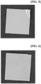
- FIGS. 5 to 8 are photographs showing a comparison of a copper foil and a silicon-coated copper foil between before and after heat treatment in air.
- FIG. 5 As a result of comparing the copper foil between before heat treatment ( FIG. 5 ) and after heat treatment at 250°C for 30 minutes ( FIG. 7 ), it can be seen that the copper foil turned dark.
- FIG. 8 As a result of comparing the silicon-coated copper foil between before heat treatment ( FIG. 6 ) and after heat treatment at 250°C for 30 minutes ( FIG. 8 ), it can be seen that the silicon-coated copper foil retained its original color.
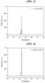
- FIGS. 3 and 4 show the XRD measurement results of a single-crystal thin copper film (SCCF) and a single-crystal copper thin film coated with silicon and then heat treated.
- SCCF single-crystal thin copper film
- FIG. 4 it can be seen that, even after coating with silicon and then heat treatment at 350°C in air for 30 minutes, the crystal structure of the silicon-coated single-crystal copper thin film did not change at all, crystallization in one direction occurred more easily, and the surface was not oxidized.
- FIGS. 9 to 10 show the XRD measurement results of a copper foil and a silicon-coated copper foil after heat treatment in air.
- the copper foil of FIG. 9 shows a Cu 2 O phase as shown in FIG. 9
- the silicon-coated copper foil retained its original copper structure as shown in in FIG. 10 .
- the silicon-coated copper of the present invention may have a resistivity of 1.68*10 -6 ⁇ cm, which is the resistivity of bulk Cu, and 2.2*10 -6 ⁇ cm, which is the resistivity of bulk Au.
- the silicon-coated copper of the present invention has an electrical resistivity similar to that of non-silicon-coated copper.
- the silicon-coated copper of the present invention is prevented from oxidation even when heated at 200°C for 60 hours.
- FIG. 11 is a graph showing changes in electrical resistivity of a SiCu/Al 2 O 3 specimen depending on the heat treatment temperature and silicon coating thickness thereof.
- zone A shows the change in resistivity of a 185-nm-thick single-crystal thin copper thin film (SCCF) specimen by heat treatment
- zone B shows the change in resistivity of a silicon-coated single-crystal thin copper thin film (SCCF) specimen (Si5SCCF) by heat treatment
- Zone C shows the change in resistivity of a single-crystal thin copper film (SCCF) specimen coated with silicon thicker than 5 nm.
- Zone D shows the resistivities of bulk Cu and bulk Au, compared to zones B and C.
- the pristine SCCF specimen has a resistivity which is almost the same as 1.68*10 -6 ⁇ cm, which is the resistivity of bulk Cu, and it has a resistivity lower than 2.2*10 -6 ⁇ cm, which is the resistivity of bulk Au.
- SCCF single-crystal thin copper film
- zone B it can be seen that a specimen (Si5SCCF) obtained by coating a 185-nm-thick single-crystal thin copper film (SCCF) with 5 nm of silicon has a resistivity similar to that of bulk Cu even when heat-treated at 400°C for 30 minutes.
- zone C shows that the resistivity changes as the thickness of the silicon layer increases.
- SCCF single-crystal thin copper film coated with silicon has a resistivity between the resistivity of bulk Cu and the resistivity of bulk Au before the thickness of the silicon layer reaches 30 nm, and has a resistivity similar to that of bulk Au only after the thickness of the silicon layer reaches 30 nm.
- the silicon-coated copper may be produced in a single-crystal thin film, polycrystalline thin film, foil, or bulk form. As shown in FIG. 11 , when the silicon-coated copper is a single-crystal thin film, it is prevented from oxidation even when heated at 400°C for 30 minutes. When the silicon-coated copper is a polycrystalline thin film, foil, or bulk, it is prevented from oxidation even when heated at 300°C for 30 minutes.
- the silicon-coated copper produced by the method for producing a silicon-coated copper includes: a copper layer 10; a SiCuO x layer 20 formed of a silicon (Si)-oxygen (O)-copper (Cu) mixture on the copper layer 10; a first silicon (Si)-oxygen (O) mixed layer 30 formed on the SiCuO x layer 20; a silicon (Si) layer 40 formed on the first silicon (Si)-oxygen (O) mixed layer 30; and a second silicon (Si)-oxygen (O) mixed layer 50 formed on the silicon layer (Si) layer 40.
- FIG. 12 shows the TEM measurement results of the cross-section of a Si10Cu/Al 2 O 3 specimen obtained by coating a single-crystal copper thin film with 10 nm of silicon.
- the coated silicon does not simply exist as a single layer, but a silicon (Si)-oxygen (O) mixed layer is formed on the copper layer 10, and a silicon (Si) layer and a silicon (Si)-oxygen (O) mixed layer are sequentially formed thereon.
- the first silicon (Si)-oxygen (O) mixed layer 30, the silicon (Si) layer 40, and the second silicon (Si)-oxygen (O) mixed layer 50 which are layers formed by coating copper with silicon (Si), may have a thickness of 5 to 30 nm. If these silicon (Si)-coated layers are thinner than 5 nm, a problem may arise in that the copper is easily oxidized, and if these layers are thicker than 30 nm, a problem may arise in that the copper becomes dielectric or has poor electrical conductivity. For this reason, these layers have a thickness within the above-described range.
- the silicon (Si) layer 40 may have a thickness of 3 to 20 nm.
- the first silicon (Si)-oxygen (O) mixed layer 30 and the second silicon (Si)-oxygen (O) mixed layer 50 may have a thickness of 1 to 10 nm.
- the SiCuO x layer may have a thickness of 0.8 to 1.2 nm.
- FIG. 13 shows the results of observing the change in distance between copper atoms depending on depth by high-resolution TEM. As shown in FIG. 13 , it can be seen that the distance between copper (Cu) atoms on the surface has decreased, which means that a mixed layer of silicon (Si) and copper (Cu) exists on the surface. The presence of this mixed layer of silicon (Si) and copper (Cu) can be confirmed again by the XPS analysis shown in FIG. 14 .
- FIG. 14 shows the results of XPS analysis performed to examine the distribution of components on the surface of the SCCF (Si10SCCF) specimen coated with 10 nm of silicon. It can be seen that the oxygen on the surface decreases slightly, increases again in the mixed layer, and then decreases, and the distribution of silicon (Si) is the highest in the portion where oxygen forms the valley. Additionally, there is a portion where oxygen, silicon, and copper form a mixed layer, and this mixed layer is expected to play a critical role in preventing oxidation.
- the silicon (Si)-oxygen (O)-copper (Cu) mixed layer 20 (SiCuO x layer), the silicon (Si)-oxygen (O) mixed layer (SiOx), and the silicon (Si) layer 40 are sequentially formed.
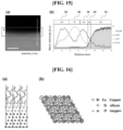
- FIG. 15 shows the surface structure (TEM) of the surface of the SCCF (Si10SCCF) specimen coated with 10 nm of silicon, from which shows the surface morphology of the silicon-coated copper can be confirmed more accurately.
- FIG. 15(b) shows the results of TEM analysis of components. As shown in the TEM measurement results in FIG. 12 and the XPS measurement results in FIG. 14 , FIG. 15(b) shows that the silicon (Si)-oxygen (O)-copper (Cu) mixed layer 20 (SiCuO x layer), the silicon (Si)-oxygen (O) mixed layer (SiOx), and the silicon (Si) layer 40 are sequentially formed on the copper (Cu) surface.
- the formed silicon (Si)-oxygen (O) mixed layer (SiO x ) has an amorphous structure, it is not visible in the image of FIG. 15(a) .
- Silicon atoms immediately above the copper thin film function to fix oxygen atoms, which move freely on the copper surface, at optimal sites. In general, oxygen atoms move relatively freely on the flat surface of copper, but silicon functions to fix these oxygen atoms.
- the thickness of the silicon (Si) layer 40 is not critical to preventing oxidation, and the most important structure is determined by 1 or 2 layers of atoms immediately above the copper thin film.
- the silicon (Si)-oxygen (O)-copper (Cu) mixed layer 20 (SiCuO x layer) including a mixture of oxygen, silicon and copper is present, and it is expected that this mixed layer plays a critical role in preventing oxidation.
- FIG. 16 shows the expected distribution of oxygen (O) and silicon (Si) in the SiCuO x layer 20 on the copper thin film.
- FIG. 16(a) is a side view showing that oxygen (O) and silicon (Si) form the SiCuO x layer 20 on the copper thin film
- FIG. 16(b) is a top view.
- the silicon (Si) is expected to bond with oxygen (O) on the copper surface and function to fix oxygen onto the copper surface.
- the most basic structure is as shown in FIG. 16 .
- the oxygen (O) covers the copper surface and is then fixed by silicon (Si)
- it may function to prevent other oxygen (O) atoms from entering the inside of the copper.
- the present invention also provides a semiconductor device including a silicon-coated copper produced by the method for producing a silicon-coated copper.
- This semiconductor device may include a copper on which a silicon (Si)-oxygen (O)-copper (Cu) mixed layer has been formed by depositing silicon (Si). Details regarding the copper in the semiconductor device are as described above with respect to the silicon-coated copper.
- the semiconductor device is connected to a semiconductor chip pad and a terminal and includes the oxidation-resistant copper of the present invention, which has the silicon (Si)-oxygen (O)-copper (Cu) mixed layer formed on the surface thereof.
- the copper in the semiconductor device of the present invention has low electrical resistance and high firmness, is less expensive, has increased resistance even to high surrounding temperatures, and may be used for a long time.
- the silicon-coated copper in the semiconductor device retains the advantages of general copper, and at the same time, has improved electrical properties and increased strength due to inhibition of oxidation.
- the first silicon (Si)-oxygen (O) mixed layer 30, the silicon (Si) layer 40, and the second silicon (Si)-oxygen (O) mixed layer 50 which are layers formed by coating copper with silicon (Si), may have a thickness of 5 to 30 nm. If these silicon (Si)-coated layers are thinner than 5 nm, a problem may arise in that the copper is easily oxidized, and if these layers are thicker than 30 nm, a problem may arise in that the copper becomes dielectric or has poor electrical conductivity. For this reason, these layers have a thickness within the above-described range.
- the SiCuO x layer may have a thickness of 0.8 to 1.2 nm.
- the present invention it is possible to produce a copper free from oxidation with high efficiency simply by deposition of silicon (Si), and it is possible to replace gold with copper (Cu) and silicon (Si), which are the most abundant on earth. Therefore, the present invention is economically highly valuable.
- a silicon-coated copper which has resistance to oxidation while retaining the electrical properties of copper, by forming a silicon (Si)-oxygen (O)-copper (Cu) mixed layer through deposition of silicon (Si).
- an oxidation-resistant copper which lasts the longest at high temperatures, is produced in a very simple manner, is inexpensive, and may be used semi-permanently at room temperature.
- the copper of the present invention may greatly enhance current density and may create a very great sensation in semiconductor processes.
Landscapes
- Chemical & Material Sciences (AREA)
- Engineering & Computer Science (AREA)
- Materials Engineering (AREA)
- Metallurgy (AREA)
- Organic Chemistry (AREA)
- Chemical Kinetics & Catalysis (AREA)
- Mechanical Engineering (AREA)
- Crystallography & Structural Chemistry (AREA)
- Inorganic Chemistry (AREA)
- Physics & Mathematics (AREA)
- Thermal Sciences (AREA)
- Physical Vapour Deposition (AREA)
- Other Surface Treatments For Metallic Materials (AREA)
- Internal Circuitry In Semiconductor Integrated Circuit Devices (AREA)
- Manufacturing & Machinery (AREA)
- Silicon Compounds (AREA)
Applications Claiming Priority (2)
| Application Number | Priority Date | Filing Date | Title |
|---|---|---|---|
| KR1020210069338A KR102640972B1 (ko) | 2021-05-28 | 2021-05-28 | 실리콘이 코팅 된 구리 제조방법, 이를 이용한 실리콘이 코팅된 산화방지용 구리 및 이를 이용한 반도체 장치 |
| PCT/KR2022/006804 WO2022250343A1 (ko) | 2021-05-28 | 2022-05-12 | 실리콘이 코팅 된 구리 제조방법, 이를 이용한 실리콘이 코팅된 산화방지용 구리 및 이를 이용한 반도체 장치 |
Publications (2)
| Publication Number | Publication Date |
|---|---|
| EP4350026A1 true EP4350026A1 (de) | 2024-04-10 |
| EP4350026A4 EP4350026A4 (de) | 2025-12-03 |
Family
ID=84230085
Family Applications (1)
| Application Number | Title | Priority Date | Filing Date |
|---|---|---|---|
| EP22811536.6A Pending EP4350026A4 (de) | 2021-05-28 | 2022-05-12 | Verfahren zur herstellung von siliciumbeschichtetem kupfer, siliciumbeschichtetes antioxidationskupfer damit und halbleiterbauelement damit |
Country Status (6)
| Country | Link |
|---|---|
| US (1) | US12595546B2 (de) |
| EP (1) | EP4350026A4 (de) |
| JP (1) | JP7715420B2 (de) |
| KR (1) | KR102640972B1 (de) |
| CN (1) | CN117222772B (de) |
| WO (1) | WO2022250343A1 (de) |
Families Citing this family (2)
| Publication number | Priority date | Publication date | Assignee | Title |
|---|---|---|---|---|
| KR102640972B1 (ko) * | 2021-05-28 | 2024-02-23 | 부산대학교 산학협력단 | 실리콘이 코팅 된 구리 제조방법, 이를 이용한 실리콘이 코팅된 산화방지용 구리 및 이를 이용한 반도체 장치 |
| KR20250010549A (ko) | 2023-07-12 | 2025-01-21 | 한국재료연구원 | 내오염성 구리계 제품 및 알루미늄계 제품의 제조 방법 |
Family Cites Families (17)
| Publication number | Priority date | Publication date | Assignee | Title |
|---|---|---|---|---|
| JPS63299250A (ja) * | 1987-05-29 | 1988-12-06 | Fujitsu Ltd | 半導体装置の製造方法 |
| EP0601509A1 (de) * | 1992-12-07 | 1994-06-15 | Nikko Kyodo Co., Ltd. | Halbleiteranordnungen und Herstellungsverfahren |
| CN1199254C (zh) * | 1999-06-28 | 2005-04-27 | 尤纳克西斯巴尔策斯公司 | 部件及其制造方法 |
| WO2006025347A1 (ja) * | 2004-08-31 | 2006-03-09 | National University Corporation Tohoku University | 銅合金及び液晶表示装置 |
| KR100598290B1 (ko) * | 2004-05-20 | 2006-07-07 | 동부일렉트로닉스 주식회사 | 리소그래피 공정의 감광막 패턴 형성 방법 |
| SE0402082L (sv) * | 2004-08-25 | 2006-04-18 | Sandvik Intellectual Property | Metallprodukt, metod för att tillverka en metallprodukt och användning av denna |
| JP2006165115A (ja) * | 2004-12-03 | 2006-06-22 | Toshiba Corp | 半導体装置 |
| JP2007266416A (ja) * | 2006-03-29 | 2007-10-11 | Nippon Foil Mfg Co Ltd | プリント配線板用金属箔とそれを用いた積層板 |
| EP2156481B1 (de) * | 2007-05-31 | 2012-10-31 | Nxp B.V. | Elektronische vorrichtung mit einer umkehrbaren struktur und verfahren zur herstellung einer elektronischen vorrichtung |
| KR20140097244A (ko) * | 2011-11-08 | 2014-08-06 | 토소우 에스엠디, 인크 | 특별한 표면 처리를 하고 양호한 입자 성능을 가진 실리콘 스퍼터링 타겟 및 그 제조 방법들 |
| KR20160108565A (ko) * | 2014-09-19 | 2016-09-19 | 미쓰이금속광업주식회사 | 표면 처리 구리박 및 그 제조 방법, 프린트 배선판용 동장 적층판, 그리고 프린트 배선판 |
| US10763002B2 (en) * | 2015-04-28 | 2020-09-01 | Mitsui Mining & Smelting Co., Ltd. | Surface-treated copper foil, manufacturing method therefor, printed circuit board copper-clad laminate, and printed circuit board |
| US9613826B2 (en) * | 2015-07-29 | 2017-04-04 | United Microelectronics Corp. | Semiconductor process for treating metal gate |
| JP2018137254A (ja) * | 2017-02-20 | 2018-08-30 | 住友金属鉱山株式会社 | 高周波基板 |
| JP6811136B2 (ja) | 2017-03-30 | 2021-01-13 | Jx金属株式会社 | Cu−Ni−Si系銅合金条及びその製造方法 |
| US10319582B2 (en) * | 2017-04-27 | 2019-06-11 | Lam Research Corporation | Methods and apparatus for depositing silicon oxide on metal layers |
| KR102640972B1 (ko) * | 2021-05-28 | 2024-02-23 | 부산대학교 산학협력단 | 실리콘이 코팅 된 구리 제조방법, 이를 이용한 실리콘이 코팅된 산화방지용 구리 및 이를 이용한 반도체 장치 |
-
2021
- 2021-05-28 KR KR1020210069338A patent/KR102640972B1/ko active Active
-
2022
- 2022-05-12 EP EP22811536.6A patent/EP4350026A4/de active Pending
- 2022-05-12 CN CN202280030045.6A patent/CN117222772B/zh active Active
- 2022-05-12 WO PCT/KR2022/006804 patent/WO2022250343A1/ko not_active Ceased
- 2022-05-12 US US18/561,672 patent/US12595546B2/en active Active
- 2022-05-12 JP JP2023572159A patent/JP7715420B2/ja active Active
Also Published As
| Publication number | Publication date |
|---|---|
| CN117222772B (zh) | 2026-01-30 |
| KR20220160997A (ko) | 2022-12-06 |
| CN117222772A (zh) | 2023-12-12 |
| JP7715420B2 (ja) | 2025-07-30 |
| KR102640972B9 (ko) | 2025-06-12 |
| US12595546B2 (en) | 2026-04-07 |
| JP2024521742A (ja) | 2024-06-04 |
| WO2022250343A1 (ko) | 2022-12-01 |
| EP4350026A4 (de) | 2025-12-03 |
| KR102640972B1 (ko) | 2024-02-23 |
| US20240250049A1 (en) | 2024-07-25 |
Similar Documents
| Publication | Publication Date | Title |
|---|---|---|
| EP4350026A1 (de) | Verfahren zur herstellung von siliciumbeschichtetem kupfer, siliciumbeschichtetes antioxidationskupfer damit und halbleiterbauelement damit | |
| US6057223A (en) | Passivated copper conductive layers for microelectronic applications | |
| US6518177B1 (en) | Method of manufacturing a semiconductor device | |
| WO2004053971A1 (ja) | 配線用銅合金、半導体装置、配線の形成方法及び半導体装置の製造方法 | |
| US4717591A (en) | Prevention of mechanical and electronic failures in heat-treated structures | |
| CN114783980B (zh) | Cu互连集成电路用多层合金扩散阻挡层及其制备方法 | |
| JP2000294738A (ja) | 薄膜抵抗体およびその製造方法 | |
| TW200539391A (en) | Method for fabricating low resistivity barrier for copper interconnect | |
| JP3021996B2 (ja) | アルミニウム配線およびその形成方法 | |
| Aboelfotoh et al. | Electrical transport properties of Cu3Ge thin films | |
| JP2534434B2 (ja) | 耐酸化性化合物およびその製造方法 | |
| Li et al. | Conductive metallic LaNiO3 films from metallo-organic precursors | |
| JP2882380B2 (ja) | 半導体装置及びその製造方法 | |
| JPS6128213B2 (de) | ||
| JPH1154511A (ja) | 半導体装置の金属配線構造及びその形成方法 | |
| Sinha et al. | Thermal stability of PtSi films on polysilicon layers | |
| JP2000124310A (ja) | 半導体装置およびその製造方法 | |
| EP0130468B1 (de) | Schutzüberzug für Leiter, um mechanisches und elektronisches Fehlen zu verhindern, besonders während thermischer Behandlung ihrer Trägerstruktur | |
| CN109346456A (zh) | 一种显示用电子器件铜互连布线电极及其制备方法 | |
| JP2001351878A (ja) | 半導体装置用WSi膜、ならびにそのWSi膜を用いた半導体装置 | |
| US6838116B2 (en) | Oxygen-removing pre-process for copper interconnect grown by electrochemical displacement deposition | |
| JPH08111455A (ja) | 配線形成方法 | |
| KR101005739B1 (ko) | 반도체 소자의 금속배선 형성 방법 | |
| JPS5844767A (ja) | 半導体装置 | |
| Oishi et al. | Orientational growth of Al (111) caused by interposing Al3Ti layer on a highly oriented TiN (200) film |
Legal Events
| Date | Code | Title | Description |
|---|---|---|---|
| STAA | Information on the status of an ep patent application or granted ep patent |
Free format text: STATUS: THE INTERNATIONAL PUBLICATION HAS BEEN MADE |
|
| PUAI | Public reference made under article 153(3) epc to a published international application that has entered the european phase |
Free format text: ORIGINAL CODE: 0009012 |
|
| STAA | Information on the status of an ep patent application or granted ep patent |
Free format text: STATUS: REQUEST FOR EXAMINATION WAS MADE |
|
| 17P | Request for examination filed |
Effective date: 20231120 |
|
| AK | Designated contracting states |
Kind code of ref document: A1 Designated state(s): AL AT BE BG CH CY CZ DE DK EE ES FI FR GB GR HR HU IE IS IT LI LT LU LV MC MK MT NL NO PL PT RO RS SE SI SK SM TR |
|
| DAV | Request for validation of the european patent (deleted) | ||
| DAX | Request for extension of the european patent (deleted) | ||
| A4 | Supplementary search report drawn up and despatched |
Effective date: 20251103 |
|
| RIC1 | Information provided on ipc code assigned before grant |
Ipc: C23C 14/06 20060101AFI20251028BHEP Ipc: C23C 14/00 20060101ALI20251028BHEP Ipc: C23C 14/16 20060101ALI20251028BHEP Ipc: C23C 14/58 20060101ALI20251028BHEP Ipc: H01L 23/00 20060101ALI20251028BHEP Ipc: H01B 1/02 20060101ALI20251028BHEP Ipc: C23C 28/00 20060101ALI20251028BHEP Ipc: C30B 23/02 20060101ALI20251028BHEP Ipc: C30B 29/06 20060101ALI20251028BHEP Ipc: H01L 23/532 20060101ALI20251028BHEP Ipc: H01L 21/285 20060101ALI20251028BHEP Ipc: C30B 29/22 20060101ALI20251028BHEP |