EP4346013B1 - Verbinder, verbinderanordnung und verbindungsverfahren - Google Patents
Verbinder, verbinderanordnung und verbindungsverfahren Download PDFInfo
- Publication number
- EP4346013B1 EP4346013B1 EP23190481.4A EP23190481A EP4346013B1 EP 4346013 B1 EP4346013 B1 EP 4346013B1 EP 23190481 A EP23190481 A EP 23190481A EP 4346013 B1 EP4346013 B1 EP 4346013B1
- Authority
- EP
- European Patent Office
- Prior art keywords
- conductor
- connection object
- electric wire
- connector
- placement surface
- Prior art date
- Legal status (The legal status is an assumption and is not a legal conclusion. Google has not performed a legal analysis and makes no representation as to the accuracy of the status listed.)
- Active
Links
Images


Classifications
-
- H—ELECTRICITY
- H01—ELECTRIC ELEMENTS
- H01R—ELECTRICALLY-CONDUCTIVE CONNECTIONS; STRUCTURAL ASSOCIATIONS OF A PLURALITY OF MUTUALLY-INSULATED ELECTRICAL CONNECTING ELEMENTS; COUPLING DEVICES; CURRENT COLLECTORS
- H01R12/00—Structural associations of a plurality of mutually-insulated electrical connecting elements, specially adapted for printed circuits, e.g. printed circuit boards [PCB], flat or ribbon cables, or like generally planar structures, e.g. terminal strips, terminal blocks; Coupling devices specially adapted for printed circuits, flat or ribbon cables, or like generally planar structures; Terminals specially adapted for contact with, or insertion into, printed circuits, flat or ribbon cables, or like generally planar structures
- H01R12/70—Coupling devices
- H01R12/77—Coupling devices for flexible printed circuits, flat or ribbon cables or like structures
- H01R12/78—Coupling devices for flexible printed circuits, flat or ribbon cables or like structures connecting to other flexible printed circuits, flat or ribbon cables or like structures
-
- H—ELECTRICITY
- H01—ELECTRIC ELEMENTS
- H01R—ELECTRICALLY-CONDUCTIVE CONNECTIONS; STRUCTURAL ASSOCIATIONS OF A PLURALITY OF MUTUALLY-INSULATED ELECTRICAL CONNECTING ELEMENTS; COUPLING DEVICES; CURRENT COLLECTORS
- H01R4/00—Electrically-conductive connections between two or more conductive members in direct contact, i.e. touching one another; Means for effecting or maintaining such contact; Electrically-conductive connections having two or more spaced connecting locations for conductors and using contact members penetrating insulation
- H01R4/28—Clamped connections, spring connections
- H01R4/48—Clamped connections, spring connections utilising a spring, clip, or other resilient member
-
- H—ELECTRICITY
- H01—ELECTRIC ELEMENTS
- H01R—ELECTRICALLY-CONDUCTIVE CONNECTIONS; STRUCTURAL ASSOCIATIONS OF A PLURALITY OF MUTUALLY-INSULATED ELECTRICAL CONNECTING ELEMENTS; COUPLING DEVICES; CURRENT COLLECTORS
- H01R12/00—Structural associations of a plurality of mutually-insulated electrical connecting elements, specially adapted for printed circuits, e.g. printed circuit boards [PCB], flat or ribbon cables, or like generally planar structures, e.g. terminal strips, terminal blocks; Coupling devices specially adapted for printed circuits, flat or ribbon cables, or like generally planar structures; Terminals specially adapted for contact with, or insertion into, printed circuits, flat or ribbon cables, or like generally planar structures
- H01R12/70—Coupling devices
- H01R12/77—Coupling devices for flexible printed circuits, flat or ribbon cables or like structures
- H01R12/778—Coupling parts carrying sockets, clips or analogous counter-contacts
-
- H—ELECTRICITY
- H01—ELECTRIC ELEMENTS
- H01R—ELECTRICALLY-CONDUCTIVE CONNECTIONS; STRUCTURAL ASSOCIATIONS OF A PLURALITY OF MUTUALLY-INSULATED ELECTRICAL CONNECTING ELEMENTS; COUPLING DEVICES; CURRENT COLLECTORS
- H01R13/00—Details of coupling devices of the kinds covered by groups H01R12/70 or H01R24/00 - H01R33/00
- H01R13/46—Bases; Cases
- H01R13/514—Bases; Cases composed as a modular blocks or assembly, i.e. composed of co-operating parts provided with contact members or holding contact members between them
-
- H—ELECTRICITY
- H01—ELECTRIC ELEMENTS
- H01R—ELECTRICALLY-CONDUCTIVE CONNECTIONS; STRUCTURAL ASSOCIATIONS OF A PLURALITY OF MUTUALLY-INSULATED ELECTRICAL CONNECTING ELEMENTS; COUPLING DEVICES; CURRENT COLLECTORS
- H01R13/00—Details of coupling devices of the kinds covered by groups H01R12/70 or H01R24/00 - H01R33/00
- H01R13/62—Means for facilitating engagement or disengagement of coupling parts or for holding them in engagement
- H01R13/629—Additional means for facilitating engagement or disengagement of coupling parts, e.g. aligning or guiding means, levers, gas pressure electrical locking indicators, manufacturing tolerances
-
- H—ELECTRICITY
- H01—ELECTRIC ELEMENTS
- H01R—ELECTRICALLY-CONDUCTIVE CONNECTIONS; STRUCTURAL ASSOCIATIONS OF A PLURALITY OF MUTUALLY-INSULATED ELECTRICAL CONNECTING ELEMENTS; COUPLING DEVICES; CURRENT COLLECTORS
- H01R4/00—Electrically-conductive connections between two or more conductive members in direct contact, i.e. touching one another; Means for effecting or maintaining such contact; Electrically-conductive connections having two or more spaced connecting locations for conductors and using contact members penetrating insulation
- H01R4/28—Clamped connections, spring connections
- H01R4/48—Clamped connections, spring connections utilising a spring, clip, or other resilient member
- H01R4/4809—Clamped connections, spring connections utilising a spring, clip, or other resilient member using a leaf spring to bias the conductor toward the busbar
Definitions
- the present invention relates to a connector, particularly to a connector and a connector assembly that electrically connect a conductor portion of an electric wire to a contact portion exposed on a bottom surface of a sheet type connection object.
- the present invention also relates to a connecting method for electrically connecting a conductor portion of an electric wire to a contact portion exposed on a bottom surface of a sheet type connection object.
- smart clothes that can obtain user's biological data such as the heart rate and the body temperature only by being worn by the user.
- Such smart clothes have an electrode disposed at a measurement site and constituted of a flexible conductor, and when a wearable device serving as a measurement device is electrically connected to the electrode, biological data can be transmitted to the wearable device.
- the electrode and the wearable device can be interconnected by, for instance, use of a connector connected to the flexible conductor.
- JP 2007-214087 A discloses a connector shown in FIG. 19 as a connector used for connecting an electric wire to a flexible conductor.
- This connector includes a first connector 2 connected to an end of a substrate 1 and a second connector 4 attached to tips of electric wires 3, and the electric wires 3 can be connected to a flexible conductor of the substrate 1 by fitting the second connector 4 to the first connector 2.
- first connector 2 and the second connector 4 that are separately attached to the end of the substrate 1 and the tips of the electric wires 3 need to be fitted to each other in order to connect the electric wires 3 to the flexible conductor of the substrate 1, and this causes a larger size of a device; and there is a separable connection portion between the first connector 2 and the second connector 4, which impairs the reliability of electric connection.
- US 5,944,553 discloses a flat cable connection structure.
- bus bars are integrally fitted to a resin-made bus-bar holder by molding, conductor exposed sections of a flat cable and conductor exposed sections of wires are connected to these bus bars either by welding or by soldering, and the flat cable is inverted to the rear surface of the bus-bar holder and is sandwiched between the bus-bar holder and an under case
- US 8,579,637 B2 discloses an electrical connection system for contacting an electronic module with multiple printed conductors of a flexible printed circuit.
- the present invention has been made to overcome the conventional problems as above and aims at providing a connector and a connector assembly that can have a small size while electrically connecting, with high reliability, a conductor portion of an electric wire to a contact portion exposed on a bottom surface of a sheet type connection object.
- the present invention also aims at providing a connecting method for electrically connecting a conductor portion of an electric wire to a contact portion exposed on a bottom surface of a sheet type connection object.
- a connector according to the present invention is one connecting a conductor portion of an electric wire to a contact portion exposed on a bottom surface of a sheet type connection object, the connector comprising:
- a connector assembly according to the present invention comprises:
- a connecting method is one for connecting a conductor portion of an electric wire to a contact portion exposed on a bottom surface of a sheet type connection object, the method comprising:
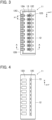
- FIG. 1 shows a connector assembly according to the embodiment.
- the connector assembly is obtained by connecting conductor portions 31A of a plurality of coated electric wires 31 to a sheet type connection object 21 by means of a connector 11.
- the connector 11 includes an insulator 12 of substantially flat plate shape made of an insulating resin material, and a plurality of metal terminals 13 retained by the insulator 12.
- the coated electric wires 31 are aligned in a predetermined alignment direction and each extend in a direction orthogonal to the alignment direction in parallel to the surface of the insulator 12 of the connector 11.
- Each coated electric wire 31 has a structure in which the outer periphery of the conductor portion 31A is covered with an insulating coating portion 31B.
- the conductor portions 31A of the plurality of coated electric wires 31 are electrically connected to a plurality of contact portions, which will be described later, exposed on the bottom surface of the connection object 21.
- the conductor portion 31A of the coated electric wire 31 may be either a so-called solid wire constituted of one conductor or a so-called stranded wire constituted of plural conductors being stranded.
- the insulator 12 of the connector 11 is defined as extending along an XY plane, the alignment direction of the coated electric wires 31 is referred to as "X direction,” the direction in which each coated electric wire 31 extends toward the connector 11 is referred to as "+Y direction,” and the direction orthogonal to an XY plane is referred to as "Z direction.”
- the insulator 12 of the connector 11 has a rectangular shape extending along an XY plane and elongated in the X direction, and has a flat surface 12A extending along the XY plane and facing the +Z direction.
- a wall portion 12B is formed to project in the +Z direction, and at the -Y directional end portion of the insulator 12, a plurality of electric-wire accommodating grooves 12C are formed to be aligned in the X direction.
- the electric-wire accommodating grooves 12C separately correspond to the coated electric wires 31, and each groove 12C extends in the Y direction across the wall portion 12B, is recessed from the flat surface 12A toward the -Z direction, and has an X directional groove width corresponding to the diameter of the coated electric wire 31.
- a plurality of protrusion portions 12D are formed near a +Y directional end portion of the insulator 12 so as to be aligned in the X direction and project in the +Z direction.
- the insulator 12 is provided with a through-hole 12E penetrating the insulator 12 in the Z direction at a position adjacent to the plurality of protrusion portions 12D, aligned in the X direction, on the -Y direction side thereof.
- the through-hole 12E extends in the X direction over all of the protrusion portions 12D aligned in the X direction.
- the plurality of metal terminals 13 are exposed on the flat surface 12A at positions adjacent to the through-hole 12E on the -Y direction side thereof.
- the electric-wire accommodating grooves 12C, the protrusion portions 12D, and the metal terminals 13 are separately aligned in the X direction with an alignment pitch P1, and when viewed in the Z direction, the electric-wire accommodating groove 12C, the protrusion portion 12D, and the metal terminal 13, which correspond to one another, are arranged on one straight line along the Y direction.
- the metal terminal 13 is formed of a single bent metal sheet and has a flat plate portion 13A extending along an XY plane, a spring portion 13B connected to a +Y directional end portion of the flat plate portion 13A, and a bottom plate portion 13D connected to a -Y directional end portion of the flat plate portion 13A via a step portion 13C and extending along the XY plane.
- the flat plate portion 13A has a top surface 13E facing in the +Z direction and is provided with two projections 13F projecting in the +Z direction from the top surface 13E.
- the two projections 13F each extend in the X direction and are disposed with a distance therebetween in the Y direction.
- the spring portion 13B forms a pressing portion that presses the sheet type connection object 21 against the conductor portion 31A drawn from the coated electric wire 31, and is formed from a rising portion 13G rising toward the +Z direction from the +Y directional end portion of the flat plate portion 13A, and an arm portion 13H bent from a +Z directional end portion of the rising portion 13G and extending in the -Y direction.
- the spring portion 13B has a cantilever shape projecting in the +Z direction from the flat plate portion 13A and extending toward the -Y direction (first direction).
- a slit 13J is formed at a middle part in the X direction of the spring portion 13B so as to extend from a -Z directional end portion of the rising portion 13G connected to the flat plate portion 13A to the vicinity of a -Y directional end portion of the arm portion 13H.
- a curved portion 13K is formed to be curved toward the +Z direction.
- the bottom plate portion 13D is disposed at a position deviated in the -Z direction from the flat plate portion 13A.
- the metal terminal 13 is retained by the insulator 12 such that the top surface 13E of the flat plate portion 13A forms the same plane as the flat surface 12A of the insulator 12 and is exposed toward the +Z direction.
- the flat surface 12A of the insulator 12 and the top surface 13E of the flat plate portion 13A of the metal terminal 13 form a conductor-portion placement surface S on which the conductor portion 31A of the coated electric wire 31 is to be placed.
- the conductor-portion placement surface S extends in the X direction (third direction) along the flat surface 12A of the insulator 12.
- the spring portion 13B of the metal terminal 13 projects in the +Z direction from the conductor-portion placement surface S, and a +Y directional end portion of the spring portion 13B is situated above the through-hole 12E penetrating the insulator 12 in the Z direction.
- the step portion 13C of the metal terminal 13 is embedded in the insulator 12, and the lower surface on the -Z direction side of the bottom plate portion 13D forms the same plane as the lower surface of the insulator 12 and is exposed from the insulator 12 toward the -Z direction.
- the bottom portion of the electric-wire accommodating groove 12C of the insulator 12 is formed by the bottom plate portion 13D of the metal terminal 13.
- a Z directional height H1 to the conductor-portion placement surface S from a top surface on the +Z directional side of the bottom plate portion 13D of the metal terminal 13 forming the bottom portion of the electric-wire accommodating groove 12C of the insulator 12 is set to be substantially equal to the thickness of the insulating coating portion 31B covering the outer periphery of the conductor portion 31A of the coated electric wire 31.
- the insulating coating portion 31B is disposed on the bottom plate portion 13D of the metal terminal 13, and the conductor portion 31A drawn from the insulating coating portion 31B is disposed on the conductor-portion placement surface S.
- the connector 11 having the thus-configured metal terminals 13 and the insulator 12 that are integrally formed can be produced by, for instance, insert molding.
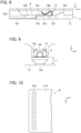
- the sheet type connection object 21 is shown in FIG. 10 .
- the connection object 21 has a multilayer structure in which at least one wiring layer formed from a conductor and a plurality of insulating layers are laminated, for instance.
- connection object 21 A top surface, extending along an XY plane and facing in the +Z direction, of the connection object 21 is covered with an insulating layer 21A.
- a plurality of opening portions 21B are formed near a -Y directional end portion of the connection object 21 so as to be aligned in the X direction and penetrate the connection object 21 in the Z direction.
- the opening portion 21B has such a size that the spring portion 13B of the metal terminal 13 projecting in the +Z direction from the conductor-portion placement surface S of the connector 11 can be passed therethrough in the Z direction.
- a plurality of contact portions 21C aligned in the X direction along the -Y directional end portion of the connection object 21 are exposed on the bottom surface, facing in the -Z direction, of the connection object 21.
- the contact portions 21C separately correspond to the opening portions 21B, and the opening portions 21B are disposed adjacent to the contact portions 21C on the +Y direction side thereof.
- the corresponding contact portion 21C is disposed adjacent to the opening portion 21B on the -Y direction side thereof at the same X directional position as that of the opening portion 21B.
- the opening portions 21B and the contact portions 21C are separately aligned in the X direction with the alignment pitch P1.
- the contact portions 21C are formed from part of one wiring layer of the connection object 21 and connected to a plurality of wiring portions (not shown) covered with the insulating layer 21D.
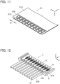
- the coated electric wires 31 are aligned in the X direction, the insulating coating portion 31B of each of the coated electric wires 31 is accommodated in the corresponding electric-wire accommodating groove 12C of the insulator 12 of the connector 11, and the conductor portion 31A drawn from the coated electric wire 31 is disposed on the conductor-portion placement surface S of the connector 11 from the -Y direction, as shown in FIG. 12 .
- the conductor portion 31A extends toward the +Y direction on the conductor-portion placement surface S formed by the flat surface 12A of the insulator 12 and the top surface 13E of the flat plate portion 13A of the metal terminal 13, and is disposed on the two protrusions 13F of the metal terminal 13.
- the conductor portion 31A is disposed between the conductor-portion placement surface S and the spring portion 13B in the state where the conductor portion 31A penetrates, in the Y direction, the slit 13J formed in the spring portion 13B of the metal terminal 13.
- connection object 21 is disposed on the connector 11 in the state where the bottom surface of the sheet type connection object 21 extending from the +Y direction (second direction) toward the conductor-portion placement surface S of the connector 11 faces the conductor-portion placement surface S.
- connection object 21 is positioned with respect to the connector 11 such that the opening portions 21B are separately situated right above the spring portions 13B of the metal terminals 13 of the connector 11.
- connection object 21 on the +Y direction side of the opening portion 21B makes contact with the top side of the protrusion portion 12D of the insulator 12 of the connector 11, while a part of the connection object 21 on the -Y direction side of the opening portion 21B is situated on the conductor portion 31A disposed on the conductor-portion placement surface S.
- the curved portion 13K formed at the -Y directional end portion of the spring portion 13B of the metal terminal 13 of the connector 11 and curved toward the +Z direction is situated on the +Z direction side of the connection object 21 through the opening portion 21B of the connection object 21.
- connection object 21 By pulling the connection object 21 in the +Y direction in this state, the connection object 21 is displaced in the +Y direction relatively to the connector 11 as shown in FIG. 18 .
- the curved portion 13K of the spring portion 13B of the metal terminal 13 of the connector 11 is situated on the +Z direction side of the connection object 21 through the opening portion 21B, a part, adjacent to the -Y direction side of the opening portion 21B, of the connection object 21 displaced in the +Y direction with respect to the spring portion 13B pushes and spread the spring portion 13B and enters the -Z directional side of the spring portion 13B.
- connection object 21 is sandwiched between the spring portion 13B passed through the opening portion 21B and the conductor portion 31A disposed on the conductor-portion placement surface S, and the contact portion 21C exposed on the bottom surface of the connection object 21 makes contact with the conductor portion 31A with predetermined contact pressure by the elastic force of the spring portion 13B and is electrically connected to the conductor portion 31A.
- connection object 21 When the connection object 21 is displaced in the +Y direction, the opening portion 21B of the connection object 21 moves to the position of the protrusion portion 21D of the insulator 12 of the connector 11, and the protrusion portion 12D is inserted in the opening portion 21B.
- the connector 11 has a simple configuration in which the plurality of metal terminals 13 are retained by the insulator 12 of substantially flat plate shape, and this makes it possible to obtain the thin connector 11 and the thin connector assembly.
- the metal terminal 13 is retained by the insulator 12 such that the +Y directional end portion of the spring portion 13B is situated above the through-hole 12E of the insulator 12, one can visually check from the -Z direction side of the connector 11 through the through-hole 12E that a +Y directional end portion of the conductor portion 31A of the coated electric wire 31 penetrates the slit 13J of the spring portion 13B of the metal terminal 13 as shown in FIGS. 17 and 18 .
- the reliability of connection of the plurality of coated electric wires 31 to the connection object 21 can be improved.
- the invention is not limited thereto, and the plurality of metal terminals 13 may also be retained by the insulator 12 by, for example, press-fitting.
- connection object 21 may be pressed against the conductor portion 31A of the coated electric wire 31 by use of a pressing portion of cantilever shape integrally formed with the insulator 12 with an insulating resin material constituting the insulator 12.
- the sheet type connection object 21 either a flexible substrate or a rigid substrate may be used.
- connection object 21 is disposed on the connector 11 such that the plurality of opening portions 21B of the connection object 21 are situated right above the spring portions 13B of the plurality of metal terminals 13 of the connector 11, and the connection object 21 is pulled in the +Y direction, whereby the plurality of contact portions 21C exposed on the bottom surface of the connection object 21 are electrically connected to the conductor portions 31A of the plurality of coated electric wires 31.
- connection object 21 even when a flexible substrate is used as the connection object 21, it is not necessary to reinforce the flexible substrate with a reinforcing plate or the like, and a plurality of contact portions of the flexible substrate can be electrically connected to the conductor portions 31A of the plurality of coated electric wires 31 with high reliability.
- a connector assembly that is deformable along the alignment direction of the plurality of coated electric wires 31 can also be configured, for instance.
- a connector assembly may be configured such that the conductor portion 31A of one coated electric wire 31 is connected to the contact portion 21C of the connection object 21 in the same manner.
- coated electric wire 31 is used as an electric wire connected to the connection object 21, an electric wire constituted only of the conductor portion 31A whose outer periphery is not covered with the insulating coating portion 31B may be connected to the connection object 21.
Landscapes
- Coupling Device And Connection With Printed Circuit (AREA)
Claims (12)
- Verbinder (11), der einen Leiterabschnitt (31A) eines elektrischen Drahtes (31) mit einem Kontaktabschnitt (21C), der an einer Unterseite eines flachmaterialartigen Verbindungsobjekts (21) frei liegt, verbindet, wobei der Verbinder umfasst:einen Isolator (12), der mindestens einen Teil einer Leiterabschnittplatzierungsfläche (S) bildet, an der der Leiterabschnitt des elektrischen Drahtes platziert ist; undeinen Drückabschnitt (13B), der von dem Isolator so gehalten wird, dass er von der Leiterabschnittsplatzierungsfläche in einer Richtung orthogonal zu der Leiterabschnittsplatzierungsfläche vorsteht und sich in einer zuvor festgelegten ersten Richtung (-Y-Richtung) entlang der Leiterabschnittsplatzierungsfläche erstreckt,dadurch gekennzeichnet, dassder Drückabschnitt in der Richtung orthogonal zu der Leiterabschnittsplatzierungsfläche elastisch verformbar ist undder Leiterabschnitt des elektrischen Drahtes, der sich von der ersten Richtung entlang der Leiterabschnittplatzierungsfläche erstreckt, zwischen der Leiterabschnittplatzierungsfläche und dem Drückabschnitt angeordnet ist und das Verbindungsobjekt zwischen dem Drückabschnitt, der durch einen Öffnungsabschnitt (21B) des Verbindungsobjekts (21) hindurch verläuft, der sich von einer zweiten Richtung (+Y-Richtung) entlang der Leiterabschnittplatzierungsfläche erstreckt, und dem Leiterabschnitt des elektrischen Drahtes sandwichartig aufgenommen ist, wobei die zweite Richtung eine der ersten Richtung entgegengesetzte Richtung ist, wodurch der Kontaktabschnitt des Verbindungsobjekts Kontakt mit dem Leiterabschnitt des elektrischen Drahtes herstellt und mit diesem elektrisch verbunden ist.
- Verbinder nach Anspruch 1, umfassend des Weiteren einen Metallanschluss (13), der von dem Isolator gehalten wird, wobei der Metallanschluss einen Flachplattenabschnitt (13A), der sich entlang der Leiterabschnittplatzierungsfläche erstreckt, und einen Federabschnitt (13B) von freitragender Form, der in einer Richtung orthogonal zu dem Flachplattenabschnitt von einem Endabschnitt in der zweiten Richtung des Flachplattenabschnitts vorsteht und sich in der ersten Richtung erstreckt, aufweist,wobei eine Oberseite des Flachplattenabschnitts zusammen mit dem Isolator die Leiterabschnittplatzierungsfläche bildet, undwobei der Federabschnitt den Drückabschnitt bildet.
- Verbinder nach Anspruch 2, wobei der Federabschnitt (13B) einen Schlitz (13J) aufweist, der sich von einem Verbindungsabschnitt zwischen dem Federabschnitt und dem Flachplattenabschnitt in der ersten Richtung erstreckt, und wobei der Leiterabschnitt (31A) des elektrischen Drahtes zwischen der Leiterabschnittplatzierungsfläche und dem Drückabschnitt in einem Zustand angeordnet ist, in dem der Leiterabschnitt durch den Schlitz hindurch verläuft.
- Verbinder nach Anspruch 2 oder 3, wobei der Flachplattenabschnitt (13A) mindestens einen Vorsprung (13F) aufweist, der in der Richtung orthogonal zu dem Flachplattenabschnitt vorsteht und Kontakt mit dem Leiterabschnitt des elektrischen Drahtes herstellt.
- Verbinder nach einem der Ansprüche 2-4, wobei ein Endabschnitt des Federabschnitts (13B) in der ersten Richtung in der Richtung orthogonal zu dem Flachplattenabschnitt (13A) gekrümmt ist.
- Verbinder nach einem der Ansprüche 2-5, wobei der Metallanschluss (13) in dem Isolator (12) durch Insert-Molding geformt ist.
- Verbinder nach einem der Ansprüche 1-6, wobei in einem Zustand, in dem der Drückabschnitt (13B) durch den Öffnungsabschnitt (21B) des Verbindungsobjekts (21) hindurchgeführt ist, der Kontaktabschnitt (21C) des Verbindungsobjekts, der in Bezug auf den Drückabschnitt in der zweiten Richtung verschoben ist, Kontakt mit dem Leiterabschnitt (31A) des elektrischen Drahtes herstellt.
- Verbinder nach Anspruch 7, wobei der Isolator (12) einen Vorsprungsabschnitt (12D) aufweist, der so angeordnet ist, dass er von dem Drückabschnitt in der zweiten Richtung getrennt ist und in der Richtung orthogonal zu der Leiterabschnittplatzierungsfläche vorsteht, und
wobei der Vorsprungsabschnitt in den Öffnungsabschnitt (21B) des Verbindungsobjekts, der in Bezug auf den Drückabschnitt in der zweiten Richtung verschoben ist, eingeführt ist. - Verbinder nach einem der Ansprüche 1-8, wobei der Isolator (12) eine den elektrischen Draht aufnehmende Nut (12C) aufweist, die an einem Endabschnitt des Isolators in der ersten Richtung ausgebildet ist und den elektrischen Draht aufnimmt.
- Verbinder nach einem der Ansprüche 1-9, wobei sich die Leiterabschnittplatzierungsfläche (S) in einer dritten Richtung (X-Richtung) orthogonal zu der ersten Richtung und der zweiten Richtung erstreckt,
wobei der Verbinder mehrere Drückabschnitte (13B) aufweist, die in der dritten Richtung ausgerichtet sind und jeweils von dem Isolator gehalten werden, wobei die mehreren Drückabschnitte jeweils den Drückabschnitt aufweisen, und wobei Leiterabschnitte mehrerer elektrischer Drähte mit mehreren Kontaktabschnitten des Verbindungsobjekts durch die mehreren Drückabschnitte elektrisch verbunden sind, wobei die Leiterabschnitte der mehreren elektrischen Drähte jeweils den Leiterabschnitt des elektrischen Drahtes aufweisen, wobei die mehreren Kontaktabschnitte jeweils den Kontaktabschnitt aufweisen. - Verbinderanordnung, umfassend:den Verbinder (11) nach einem der Ansprüche 1-10;das Verbindungsobjekt (21); undden elektrischen Draht (31),wobei das Verbindungsobjekt den Kontaktabschnitt (21C), der an einer Unterseite eines Endabschnitts in der ersten Richtung des Verbindungsobjekts angeordnet ist, und den Öffnungsabschnitt (21B), der neben dem Kontaktabschnitt an einer Seite der zweiten Richtung des Kontaktabschnitts angeordnet ist, aufweist.
- Verbindungsverfahren zum Verbinden eines Leiterabschnitts (31A) eines elektrischen Drahtes (31) mit einem Kontaktabschnitt (21C), der an einer Unterseite eines flachmaterialartigen Verbindungsobjekts (21) frei liegt, wobei das Verfahren umfasst:Anordnen des Leiterabschnitts (31A) des elektrischen Drahtes an einer Leiterabschnittplatzierungsfläche (S) eines Verbinders (11), wobei sich der Leiterabschnitt von einer zuvor festgelegten ersten Richtung (-Y-Richtung) zu einer zweiten Richtung (+Y-Richtung) erstreckt, die eine der ersten Richtung entgegengesetzte Richtung ist,Hindurchführen eines Drückabschnitts (13B) durch einen Öffnungsabschnitt (21B) des Verbindungsobjekts, der sich von der zweiten Richtung entlang der Leiterabschnittplatzierungsfläche erstreckt, wobei der Drückabschnitt von der Leiterabschnittplatzierungsfläche in einer Richtung orthogonal zu der Leiterabschnittplatzierungsfläche vorsteht und sich in der ersten Richtung erstreckt, undVerschieben des Verbindungsobjekts in der zweiten Richtung in Bezug auf den Drückabschnitt, um das Verbindungsobjekt zwischen dem Leiterabschnitt des elektrischen Drahtes und dem Drückabschnitt sandwichartig aufzunehmen, wodurch der Kontaktabschnitt des Verbindungsobjekts Kontakt mit dem Leiterabschnitt des elektrischen Drahtes herstellt und mit diesem elektrisch verbunden wird.
Applications Claiming Priority (1)
| Application Number | Priority Date | Filing Date | Title |
|---|---|---|---|
| JP2022156650A JP7822294B2 (ja) | 2022-09-29 | 2022-09-29 | コネクタ、コネクタ組立体および接続方法 |
Publications (2)
| Publication Number | Publication Date |
|---|---|
| EP4346013A1 EP4346013A1 (de) | 2024-04-03 |
| EP4346013B1 true EP4346013B1 (de) | 2025-01-22 |
Family
ID=87567366
Family Applications (1)
| Application Number | Title | Priority Date | Filing Date |
|---|---|---|---|
| EP23190481.4A Active EP4346013B1 (de) | 2022-09-29 | 2023-08-09 | Verbinder, verbinderanordnung und verbindungsverfahren |
Country Status (4)
| Country | Link |
|---|---|
| US (1) | US12463358B2 (de) |
| EP (1) | EP4346013B1 (de) |
| JP (1) | JP7822294B2 (de) |
| CN (1) | CN117791208A (de) |
Family Cites Families (11)
| Publication number | Priority date | Publication date | Assignee | Title |
|---|---|---|---|---|
| US3993383A (en) * | 1975-06-02 | 1976-11-23 | Vincent Marino | Printed circuit electrical connectors |
| JPH041663Y2 (de) * | 1985-06-17 | 1992-01-21 | ||
| JP3140683B2 (ja) * | 1996-05-27 | 2001-03-05 | 矢崎総業株式会社 | フラットケーブルの接続構造 |
| JP2004087331A (ja) | 2002-08-27 | 2004-03-18 | Fujikura Ltd | 接続ユニット |
| US6880241B2 (en) | 2002-09-30 | 2005-04-19 | General Electric Company A New York Corporation | Method for connecting coaxial cables to a printed circuit board |
| JP2007214087A (ja) | 2006-02-13 | 2007-08-23 | Fujikura Ltd | コネクタ |
| DE102010039185A1 (de) | 2010-08-11 | 2012-02-16 | Robert Bosch Gmbh | Elektrische Verbindungsanordnung |
| JP6959839B2 (ja) * | 2017-11-20 | 2021-11-05 | 日本航空電子工業株式会社 | コネクタ |
| JP7216556B2 (ja) * | 2019-01-22 | 2023-02-01 | 日本航空電子工業株式会社 | 被覆導線の接続方法、被覆導線の接続構造および被覆導線の接続部材 |
| US11258189B2 (en) * | 2019-10-03 | 2022-02-22 | Japan Aviation Electronics Industry, Limited | Connector and connecting method |
| JP7386147B2 (ja) | 2020-11-06 | 2023-11-24 | ヒロセ電機株式会社 | 平型導体用電気コネクタ |
-
2022
- 2022-09-29 JP JP2022156650A patent/JP7822294B2/ja active Active
-
2023
- 2023-08-01 CN CN202310961049.2A patent/CN117791208A/zh active Pending
- 2023-08-09 EP EP23190481.4A patent/EP4346013B1/de active Active
- 2023-08-16 US US18/450,834 patent/US12463358B2/en active Active
Also Published As
| Publication number | Publication date |
|---|---|
| US20240113453A1 (en) | 2024-04-04 |
| JP2024050058A (ja) | 2024-04-10 |
| CN117791208A (zh) | 2024-03-29 |
| JP7822294B2 (ja) | 2026-03-02 |
| US12463358B2 (en) | 2025-11-04 |
| EP4346013A1 (de) | 2024-04-03 |
Similar Documents
| Publication | Publication Date | Title |
|---|---|---|
| US7547214B2 (en) | Edge-to-edge connector system for electronic devices | |
| CN100531513C (zh) | 印刷布线板的连接装置 | |
| US10630004B2 (en) | Connection assisting member and circuit board assembly | |
| EP3435489B1 (de) | Verbinder und leiterplattenanordnung | |
| CN100534260C (zh) | 印刷布线板的连接装置 | |
| US6309223B1 (en) | Terminal assembly for flexible circuit strip | |
| JP2024001999A (ja) | コネクタ、コネクタ対及びその製造方法 | |
| EP4213308B1 (de) | Verbinder | |
| US5964594A (en) | Electrical connector | |
| EP4346013B1 (de) | Verbinder, verbinderanordnung und verbindungsverfahren | |
| EP3683895B1 (de) | Verbinder, leiterplatteanordnung und verbinderstruktur | |
| EP4293832B1 (de) | Hochfrequenzsignalübertragungsvorrichtung und elektrisches verbindungsverfahren für leiterplatte und verbinder | |
| CN118117364A (zh) | 连接器组装体和连接方法 | |
| EP4343974B1 (de) | Verbinder | |
| JPH08148204A (ja) | フラットケーブルの接続方法及びコネクタ | |
| JP7837843B2 (ja) | コネクタ | |
| EP4379964B1 (de) | Verbinderanordnung und verbindungsverfahren | |
| EP4387004B1 (de) | Verbinder | |
| CN103296524A (zh) | 连接器 | |
| JPH1032062A (ja) | 電気コネクタ | |
| KR101160901B1 (ko) | 한쌍의 헤더 콘택트 및 이것을 이용한 헤더 커넥터 | |
| CN119812810A (zh) | 端子模组、端子模组的制造方法以及端子模组的应用 | |
| JPH08203624A (ja) | 電気コネクタ |
Legal Events
| Date | Code | Title | Description |
|---|---|---|---|
| PUAI | Public reference made under article 153(3) epc to a published international application that has entered the european phase |
Free format text: ORIGINAL CODE: 0009012 |
|
| STAA | Information on the status of an ep patent application or granted ep patent |
Free format text: STATUS: REQUEST FOR EXAMINATION WAS MADE |
|
| 17P | Request for examination filed |
Effective date: 20230809 |
|
| AK | Designated contracting states |
Kind code of ref document: A1 Designated state(s): AL AT BE BG CH CY CZ DE DK EE ES FI FR GB GR HR HU IE IS IT LI LT LU LV MC ME MK MT NL NO PL PT RO RS SE SI SK SM TR |
|
| RBV | Designated contracting states (corrected) |
Designated state(s): AL AT BE BG CH CY CZ DE DK EE ES FI FR GB GR HR HU IE IS IT LI LT LU LV MC ME MK MT NL NO PL PT RO RS SE SI SK SM TR |
|
| GRAP | Despatch of communication of intention to grant a patent |
Free format text: ORIGINAL CODE: EPIDOSNIGR1 |
|
| STAA | Information on the status of an ep patent application or granted ep patent |
Free format text: STATUS: GRANT OF PATENT IS INTENDED |
|
| RIC1 | Information provided on ipc code assigned before grant |
Ipc: H01R 12/78 20110101ALI20240906BHEP Ipc: H01R 12/77 20110101ALI20240906BHEP Ipc: H01R 4/48 20060101AFI20240906BHEP |
|
| INTG | Intention to grant announced |
Effective date: 20240924 |
|
| RAP3 | Party data changed (applicant data changed or rights of an application transferred) |
Owner name: JAPAN AVIATION ELECTRONICS INDUSTRY, LIMITED |
|
| GRAS | Grant fee paid |
Free format text: ORIGINAL CODE: EPIDOSNIGR3 |
|
| GRAA | (expected) grant |
Free format text: ORIGINAL CODE: 0009210 |
|
| STAA | Information on the status of an ep patent application or granted ep patent |
Free format text: STATUS: THE PATENT HAS BEEN GRANTED |
|
| AK | Designated contracting states |
Kind code of ref document: B1 Designated state(s): AL AT BE BG CH CY CZ DE DK EE ES FI FR GB GR HR HU IE IS IT LI LT LU LV MC ME MK MT NL NO PL PT RO RS SE SI SK SM TR |
|
| REG | Reference to a national code |
Ref country code: GB Ref legal event code: FG4D |
|
| REG | Reference to a national code |
Ref country code: CH Ref legal event code: EP |
|
| REG | Reference to a national code |
Ref country code: IE Ref legal event code: FG4D |
|
| REG | Reference to a national code |
Ref country code: DE Ref legal event code: R096 Ref document number: 602023001758 Country of ref document: DE |
|
| REG | Reference to a national code |
Ref country code: NL Ref legal event code: MP Effective date: 20250122 |
|
| PG25 | Lapsed in a contracting state [announced via postgrant information from national office to epo] |
Ref country code: NL Free format text: LAPSE BECAUSE OF FAILURE TO SUBMIT A TRANSLATION OF THE DESCRIPTION OR TO PAY THE FEE WITHIN THE PRESCRIBED TIME-LIMIT Effective date: 20250122 |
|
| PG25 | Lapsed in a contracting state [announced via postgrant information from national office to epo] |
Ref country code: RS Free format text: LAPSE BECAUSE OF FAILURE TO SUBMIT A TRANSLATION OF THE DESCRIPTION OR TO PAY THE FEE WITHIN THE PRESCRIBED TIME-LIMIT Effective date: 20250422 |
|
| PG25 | Lapsed in a contracting state [announced via postgrant information from national office to epo] |
Ref country code: FI Free format text: LAPSE BECAUSE OF FAILURE TO SUBMIT A TRANSLATION OF THE DESCRIPTION OR TO PAY THE FEE WITHIN THE PRESCRIBED TIME-LIMIT Effective date: 20250122 |
|
| PG25 | Lapsed in a contracting state [announced via postgrant information from national office to epo] |
Ref country code: PL Free format text: LAPSE BECAUSE OF FAILURE TO SUBMIT A TRANSLATION OF THE DESCRIPTION OR TO PAY THE FEE WITHIN THE PRESCRIBED TIME-LIMIT Effective date: 20250122 |
|
| PG25 | Lapsed in a contracting state [announced via postgrant information from national office to epo] |
Ref country code: ES Free format text: LAPSE BECAUSE OF FAILURE TO SUBMIT A TRANSLATION OF THE DESCRIPTION OR TO PAY THE FEE WITHIN THE PRESCRIBED TIME-LIMIT Effective date: 20250122 |
|
| REG | Reference to a national code |
Ref country code: LT Ref legal event code: MG9D |
|
| PG25 | Lapsed in a contracting state [announced via postgrant information from national office to epo] |
Ref country code: IS Free format text: LAPSE BECAUSE OF FAILURE TO SUBMIT A TRANSLATION OF THE DESCRIPTION OR TO PAY THE FEE WITHIN THE PRESCRIBED TIME-LIMIT Effective date: 20250522 Ref country code: NO Free format text: LAPSE BECAUSE OF FAILURE TO SUBMIT A TRANSLATION OF THE DESCRIPTION OR TO PAY THE FEE WITHIN THE PRESCRIBED TIME-LIMIT Effective date: 20250422 |
|
| REG | Reference to a national code |
Ref country code: AT Ref legal event code: MK05 Ref document number: 1762182 Country of ref document: AT Kind code of ref document: T Effective date: 20250122 |
|
| PG25 | Lapsed in a contracting state [announced via postgrant information from national office to epo] |
Ref country code: HR Free format text: LAPSE BECAUSE OF FAILURE TO SUBMIT A TRANSLATION OF THE DESCRIPTION OR TO PAY THE FEE WITHIN THE PRESCRIBED TIME-LIMIT Effective date: 20250122 |
|
| PG25 | Lapsed in a contracting state [announced via postgrant information from national office to epo] |
Ref country code: LV Free format text: LAPSE BECAUSE OF FAILURE TO SUBMIT A TRANSLATION OF THE DESCRIPTION OR TO PAY THE FEE WITHIN THE PRESCRIBED TIME-LIMIT Effective date: 20250122 Ref country code: PT Free format text: LAPSE BECAUSE OF FAILURE TO SUBMIT A TRANSLATION OF THE DESCRIPTION OR TO PAY THE FEE WITHIN THE PRESCRIBED TIME-LIMIT Effective date: 20250522 |
|
| PG25 | Lapsed in a contracting state [announced via postgrant information from national office to epo] |
Ref country code: BG Free format text: LAPSE BECAUSE OF FAILURE TO SUBMIT A TRANSLATION OF THE DESCRIPTION OR TO PAY THE FEE WITHIN THE PRESCRIBED TIME-LIMIT Effective date: 20250122 Ref country code: GR Free format text: LAPSE BECAUSE OF FAILURE TO SUBMIT A TRANSLATION OF THE DESCRIPTION OR TO PAY THE FEE WITHIN THE PRESCRIBED TIME-LIMIT Effective date: 20250423 |
|
| PG25 | Lapsed in a contracting state [announced via postgrant information from national office to epo] |
Ref country code: AT Free format text: LAPSE BECAUSE OF FAILURE TO SUBMIT A TRANSLATION OF THE DESCRIPTION OR TO PAY THE FEE WITHIN THE PRESCRIBED TIME-LIMIT Effective date: 20250122 |
|
| PG25 | Lapsed in a contracting state [announced via postgrant information from national office to epo] |
Ref country code: SE Free format text: LAPSE BECAUSE OF FAILURE TO SUBMIT A TRANSLATION OF THE DESCRIPTION OR TO PAY THE FEE WITHIN THE PRESCRIBED TIME-LIMIT Effective date: 20250122 |
|
| PG25 | Lapsed in a contracting state [announced via postgrant information from national office to epo] |
Ref country code: SM Free format text: LAPSE BECAUSE OF FAILURE TO SUBMIT A TRANSLATION OF THE DESCRIPTION OR TO PAY THE FEE WITHIN THE PRESCRIBED TIME-LIMIT Effective date: 20250122 |
|
| PG25 | Lapsed in a contracting state [announced via postgrant information from national office to epo] |
Ref country code: DK Free format text: LAPSE BECAUSE OF FAILURE TO SUBMIT A TRANSLATION OF THE DESCRIPTION OR TO PAY THE FEE WITHIN THE PRESCRIBED TIME-LIMIT Effective date: 20250122 |
|
| PGFP | Annual fee paid to national office [announced via postgrant information from national office to epo] |
Ref country code: DE Payment date: 20250821 Year of fee payment: 3 |
|
| PG25 | Lapsed in a contracting state [announced via postgrant information from national office to epo] |
Ref country code: IT Free format text: LAPSE BECAUSE OF FAILURE TO SUBMIT A TRANSLATION OF THE DESCRIPTION OR TO PAY THE FEE WITHIN THE PRESCRIBED TIME-LIMIT Effective date: 20250122 |
|
| PGFP | Annual fee paid to national office [announced via postgrant information from national office to epo] |
Ref country code: FR Payment date: 20250828 Year of fee payment: 3 |
|
| PG25 | Lapsed in a contracting state [announced via postgrant information from national office to epo] |
Ref country code: EE Free format text: LAPSE BECAUSE OF FAILURE TO SUBMIT A TRANSLATION OF THE DESCRIPTION OR TO PAY THE FEE WITHIN THE PRESCRIBED TIME-LIMIT Effective date: 20250122 Ref country code: CZ Free format text: LAPSE BECAUSE OF FAILURE TO SUBMIT A TRANSLATION OF THE DESCRIPTION OR TO PAY THE FEE WITHIN THE PRESCRIBED TIME-LIMIT Effective date: 20250122 |
|
| REG | Reference to a national code |
Ref country code: DE Ref legal event code: R097 Ref document number: 602023001758 Country of ref document: DE |
|
| PG25 | Lapsed in a contracting state [announced via postgrant information from national office to epo] |
Ref country code: RO Free format text: LAPSE BECAUSE OF FAILURE TO SUBMIT A TRANSLATION OF THE DESCRIPTION OR TO PAY THE FEE WITHIN THE PRESCRIBED TIME-LIMIT Effective date: 20250122 |
|
| PG25 | Lapsed in a contracting state [announced via postgrant information from national office to epo] |
Ref country code: SK Free format text: LAPSE BECAUSE OF FAILURE TO SUBMIT A TRANSLATION OF THE DESCRIPTION OR TO PAY THE FEE WITHIN THE PRESCRIBED TIME-LIMIT Effective date: 20250122 |
|
| PLBE | No opposition filed within time limit |
Free format text: ORIGINAL CODE: 0009261 |
|
| STAA | Information on the status of an ep patent application or granted ep patent |
Free format text: STATUS: NO OPPOSITION FILED WITHIN TIME LIMIT |
|
| 26N | No opposition filed |
Effective date: 20251023 |