EP4297280B1 - Digital-to-analog converter - Google Patents
Digital-to-analog converter Download PDFInfo
- Publication number
- EP4297280B1 EP4297280B1 EP21931446.5A EP21931446A EP4297280B1 EP 4297280 B1 EP4297280 B1 EP 4297280B1 EP 21931446 A EP21931446 A EP 21931446A EP 4297280 B1 EP4297280 B1 EP 4297280B1
- Authority
- EP
- European Patent Office
- Prior art keywords
- current
- terminal
- switch transistor
- transistor
- switch
- Prior art date
- Legal status (The legal status is an assumption and is not a legal conclusion. Google has not performed a legal analysis and makes no representation as to the accuracy of the status listed.)
- Active
Links
Images


Classifications
-
- H—ELECTRICITY
- H03—ELECTRONIC CIRCUITRY
- H03M—CODING; DECODING; CODE CONVERSION IN GENERAL
- H03M1/00—Analogue/digital conversion; Digital/analogue conversion
- H03M1/66—Digital/analogue converters
-
- H—ELECTRICITY
- H03—ELECTRONIC CIRCUITRY
- H03M—CODING; DECODING; CODE CONVERSION IN GENERAL
- H03M1/00—Analogue/digital conversion; Digital/analogue conversion
- H03M1/66—Digital/analogue converters
- H03M1/74—Simultaneous conversion
- H03M1/742—Simultaneous conversion using current sources as quantisation value generators
- H03M1/745—Simultaneous conversion using current sources as quantisation value generators with weighted currents
Definitions
- the present disclosure relates to a digital-to-analog converter that converts a digital signal into an analog signal.
- Some digital-to-analog converters are configured such that an output load is a capacitor (capacitive load), and a current generator is connected in parallel to the capacitor.
- This digital-to-analog converter generates an analog waveform of a voltage in a capacitor by arbitrarily switching between operation and stop of a current generator using a digital signal.
- a driver circuit is generally provided in each current generator in order to switch timing between operation and stop of the current generator.
- Non-Patent Literature 1 discloses a digital-to-analog converter in which a current generator includes a transistor, and a driver circuit for driving the transistor is connected to the transistor (see Fig. 3 in Non-Patent Literature 1).
- WEIS MARKUS ET AL "Integrated 2-b Riemann Pump RF-DAC in GaN Technology for 5G Base Stations", 2019 IEEE MTT-S INTERNATIONAL MICROWAVE SYMPOSIUM (IMS), IEEE, 2 June 2019 (2019-06-02), pages 1426-1429 , presents the experimental verification of radio frequency (RF) signals with several volts of voltage swing, generated by an integrated 2-b Riemann Pump in gallium nitride (GaN) technology.
- RF radio frequency
- Non-Patent Literature 1 Weiss, M., et. al. "Integrated 2-b Riemann Pump RF-DAC in GaN Technology for 5G Base Stations". 2019 IEEE International microwave symposium (IMS) .
- a driver circuit and an input terminal for inputting a digital signal to the driver circuit are required for one current generator.
- two current generators are required for one bit
- two driver circuits and two input terminals are required for one bit, and there is a problem that the circuit size is large.
- the present disclosure has been made to solve the above problem, and an object of the present disclosure is to provide a digital-to-analog converter having a small circuit size per 1-bit element.
- the present invention provides a digital-to-analog converter according to claim 1.
- the current supply switch 41 switches connection and non-connection with the power supply terminal 30, allows a current to flow from the power supply terminal 30 in the connected state, and does not allow a current to flow from the power supply terminal 30 in the non-connection state.
- the current discharge switch 42 in the switching circuit of the nth 1-bit element 10-n is, for example, an N-type and normally-on type transistor (current discharge switch transistor).
- the current discharge switch 42 is a transistor that performs switching so that a current flows from the drain terminal D to the source terminal S in a state where a voltage of 0 V or more is applied to the gate terminal G, and when a voltage having a negative gate-source potential is applied to the gate terminal G, a current does not flow from the drain terminal D to the source terminal S.
- the current discharge switch 42 switches charge or discharge between the 1-bit element 10-n and the capacitive load 70.
- control switch 43 in the switching circuit of the nth 1-bit element 10-n is, for example, an N-type and normally-on type transistor (control switch transistor).
- the control switch 43 is a transistor that performs switching so that a current flows from the drain terminal D to the source terminal S in a state where a voltage of 0 V or more is applied to the gate terminal G, and when a voltage having a negative gate-source potential is applied to the gate terminal G, a current does not flow from the drain terminal D to the source terminal S.
- the control switch 43 switches the current supply switch transistor to the non-connection state by discharging the charge from each of the 1-bit element 10-n and the capacitive load 70 according to the value indicated by the input digital signal.
- the size of the transistor of the control switch 43 is designed to be sufficiently larger than the size of the transistor of the current supply switch 41 and the size of the transistor of the current discharge switch 42. In other words, the control switch 43 allows a current to flow more easily than the current supply switch 41 and the current discharge switch 42.
- the source terminal S of the current supply switch 41 (current supply switch transistor) and the drain terminal D of the current discharge switch 42 (current discharge switch transistor) are connected.
- the source terminal S of the current discharge switch 42 (current discharge switch transistor) and the drain terminal D of the control switch 43 (control switch transistor) are connected.
- the gate terminal G of the current supply switch 41 current supply switch transistor
- the gate terminal G of the current discharge switch 42 current discharge switch transistor
- the source terminal S of the current discharge switch 42 current discharge switch transistor
- the drain terminal D and the power supply terminal of the current supply switch 41 are connected.
- the source terminal S of the current supply switch 41 (current supply switch transistor) and the drain terminal D of the current discharge switch 42 (current discharge switch transistor) are connected to the nth bit unit output terminal 50-n and the output terminal 60.
- control switch 43 control switch transistor
- the gate terminal G of the control switch 43 (control switch transistor) and the nth input terminal 20-n are connected.
- the nth 1-bit element 10-n charges a current at the output terminal 60 in a case where the digital signal indicates low voltage or off.
- the nth 1-bit element 10-n discharges a current from the output terminal 60 in a case where the digital signal indicates a high voltage or on.
- the charge and discharge current values can be determined by the sizes of the transistors constituting the current supply switch 41 and the current discharge switch 42.
- the charge current value is determined by the size of the current supply switch transistor constituting the current supply switch 41. Further, the discharge current value is determined by the size of the current discharge switch transistor constituting the current discharge switch 42.
- the current value I n from the nth 1-bit element is set to the current value of the following Formula (2).
- I n 2 n ⁇ 1 I 0
- I 0 is any current value.
- a current value I out flowing to the output terminal is expressed by the following Formula (3).
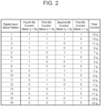
- FIG. 2 is a table showing possible patterns of current values in a case where the digital-to-analog converter according to the first embodiment of the present disclosure includes four 1-bit elements.
- any voltage waveform can be created by the digital signal according to Formula (1).
- a desired analog voltage waveform can be generated by inputting a digital signal corresponding to a value obtained by time-differentiating a desired analog voltage waveform.
- FIG. 3 is a diagram for explaining the operation of the 1-bit elements 10 of the digital-to-analog converter 1 according to the first embodiment of the present disclosure.
- parts (a), (b), (c), (d), and (e) each indicate time changes due to on and off of the control switch 43 in the nth 1-bit element 10-n.
- these parts are each described as FIGS. 3(a), 3(b), 3(c), 3(d), and 3(e) .
- N-type and normally-on type transistors are used as the current supply switch 41, the current discharge switch 42, and the control switch 43.
- FIG. 3(a) illustrates a state of the nth 1-bit element 10-n immediately before the control switch 43 is turned on.
- the voltage value V out appearing at the bit unit output terminal 50 of the nth 1-bit element 10-n is 10 V.
- the current discharge switch 42 is normally on and a current flows therethrough, and the voltage at each of the gate terminal G of the current supply switch 41, the gate terminal G of the current discharge switch 42, and the source terminal S of the current discharge switch 42 is 10 V As a result, the voltage between these and the drain terminal D of the control switch 43 is 15 V. In addition, the voltage value V out appearing at the bit unit output terminal 50 is 10 V
- FIG. 3(b) illustrates a state immediately after the control switch 43 is turned on from the state of FIG. 3(a) .
- the current flowing through the control switch 43 can be divided into three components.
- the currents of the three components are the following (current component 1), (current component 2), and (current component 3).
- Current component 1 Current (hereinafter, referred to as a "first current”) from the power supply terminal 30 via the current supply switch 41, the current discharge switch 42, and the control switch 43.
- (Current component 2) Current (hereinafter, referred to as a "second current") from the bit unit output terminal 50 via the current discharge switch 42 and the control switch 43.
- (Current component 3) Current (hereinafter, referred to as a "third current") from a line connecting the gate terminal G of the current supply switch 41 and the gate terminal G of the current discharge switch 42 via only the control switch 43.
- the third current value (4I 0 ) is the largest, and the first current value and the second current value are sufficiently smaller than the third current value.
- the current source of the third current is charges accumulated at the gate end of the current supply switch 41 and the gate end of the current discharge switch 42.
- the current supply switch 41 is switched from on to off (ON ⁇ OFF) by the change in the self-bias of the nth 1-bit element 10-n. Then, the state illustrated in FIG. 3(c) is obtained (OFF).
- control switch 43 is turned off by the digital signal input to the nth 1-bit element 10-n.
- FIG. 3(d) illustrates a state immediately after the control switch 43 is turned off from the state of FIG. 3(c) .
- the control switch 43 is turned off in the nth 1-bit element 10-n, the current flowing through the current discharge switch 42 is used for charging (0 V ⁇ 8.8 V) at the gate terminal G of the current supply switch 41 and the gate terminal G of the current discharge switch 42.
- the current supply switch 41 is thereby switched from off to on (OFF ⁇ ON) by a change in the self-bias of the nth 1-bit element 10-n.
- FIG. 3(e) illustrates a state in which the current supply switch 41 is switched on.
- the bit unit output terminal 50 is charged via the current supply switch 41, and the potential at the bit unit output terminal 50 rises at a desired slope (8.8 V ⁇ 10 V).
- the self-bias is changed according to the digital signal from one input terminal to control the voltage applied to the gate terminal G of the current supply switch 41 and the gate terminal G of the current discharge switch 42, the current supply switch 41 and the current discharge switch 42 can be switched, the potential of the bit unit output terminal 50 can be changed, and a circuit operating with one input terminal can be implemented without providing a driver circuit.
- the digital-to-analog converter includes a plurality of 1-bit elements each of which outputs a current corresponding to a value indicated by a digital signal when the digital signal is input; and a capacitive load connected to the plurality of 1-bit elements, the digital-to-analog converter being configured to generate an analog voltage waveform via the capacitive load that receives currents output from the plurality of 1-bit elements, wherein each of the 1-bit elements includes a switching circuit to change a bias of a voltage in each of the 1-bit elements according to a value indicated by an input digital signal, and to switch connection and non-connection with a power supply according to a change in the bias.
- the switching circuit includes: a current supply switch transistor to switch connection and non-connection with the power supply; a current discharge switch transistor to switch discharge between each of the 1-bit elements and the capacitive load; and a control switch transistor to switch the current supply switch transistor to a non-connection state by discharging the charge from each of the 1-bit elements and the capacitive load according to the value indicated by the input digital signal.
- the digital-to-analog converter according to the first embodiment of the present disclosure is configured in such a manner that a source terminal of the current supply switch transistor and a drain terminal of the current discharge switch transistor are connected to each other, a source terminal of the current discharge switch transistor and a drain terminal of the control switch transistor are connected to each other, a gate terminal of the current supply switch transistor, a gate terminal of the current discharge switch transistor, and a source terminal of the current discharge switch transistor are connected to each other, a drain terminal of the current supply switch transistor is connected to a power supply terminal, a source terminal of the current supply switch transistor and a drain terminal of the current discharge switch transistor are connected to an output terminal, a source terminal of the control switch transistor is grounded, and a gate terminal of the control switch transistor is connected to an input terminal thereof.
- each of the current supply switch transistor, the current discharge switch transistor, and the control switch transistor is a transistor that performs switching so that a current does not flow between a drain terminal and a source terminal when a voltage having a negative gate-source potential is applied to a gate terminal.
- the digital-to-analog converter can be configured to have a small circuit size per 1-bit element, the digital-to-analog converter is suitable for use in, for example, a high-frequency digital-to-analog converter, a communication device including a high-frequency digital-to-analog converter, or the like.
Landscapes
- Engineering & Computer Science (AREA)
- Theoretical Computer Science (AREA)
- Analogue/Digital Conversion (AREA)
Applications Claiming Priority (1)
| Application Number | Priority Date | Filing Date | Title |
|---|---|---|---|
| PCT/JP2021/010469 WO2022195692A1 (ja) | 2021-03-16 | 2021-03-16 | デジタルアナログ変換機 |
Publications (3)
| Publication Number | Publication Date |
|---|---|
| EP4297280A1 EP4297280A1 (en) | 2023-12-27 |
| EP4297280A4 EP4297280A4 (en) | 2024-04-24 |
| EP4297280B1 true EP4297280B1 (en) | 2025-05-07 |
Family
ID=83320035
Family Applications (1)
| Application Number | Title | Priority Date | Filing Date |
|---|---|---|---|
| EP21931446.5A Active EP4297280B1 (en) | 2021-03-16 | 2021-03-16 | Digital-to-analog converter |
Country Status (5)
| Country | Link |
|---|---|
| US (1) | US12355466B2 (https=) |
| EP (1) | EP4297280B1 (https=) |
| JP (1) | JP7378663B2 (https=) |
| CN (1) | CN116982261A (https=) |
| WO (1) | WO2022195692A1 (https=) |
Families Citing this family (1)
| Publication number | Priority date | Publication date | Assignee | Title |
|---|---|---|---|---|
| US12160256B2 (en) * | 2021-12-22 | 2024-12-03 | Xilinx, Inc. | DAC-based transmit driver architecture with improved bandwidth |
Family Cites Families (9)
| Publication number | Priority date | Publication date | Assignee | Title |
|---|---|---|---|---|
| JPS5513545A (en) * | 1978-07-14 | 1980-01-30 | Nippon Telegr & Teleph Corp <Ntt> | Semiconductor d-a converter |
| JPS56147519A (en) * | 1980-04-18 | 1981-11-16 | Nec Corp | Digital-to-analog converter |
| JP3209967B2 (ja) * | 1998-11-04 | 2001-09-17 | 沖電気工業株式会社 | 電流セル及びこれを用いたディジタル/アナログ変換器 |
| JP2001211076A (ja) * | 2000-01-26 | 2001-08-03 | Thine Electronics Inc | 半導体集積回路装置 |
| KR101705159B1 (ko) * | 2010-12-16 | 2017-02-10 | 한국전자통신연구원 | 전류스위치 구동회로 및 디지털 아날로그 신호변환기 |
| FR3005815B1 (fr) | 2013-05-17 | 2019-09-20 | Thales | Systeme de generation d'un signal analogique |
| WO2015004829A1 (ja) * | 2013-07-11 | 2015-01-15 | パナソニック株式会社 | 電流型d/a変換器、デルタシグマ変調器および通信装置 |
| US10499150B2 (en) * | 2016-07-05 | 2019-12-03 | Knowles Electronics, Llc | Microphone assembly with digital feedback loop |
| CN222476837U (zh) | 2023-03-31 | 2025-02-14 | 意法半导体国际公司 | 器件 |
-
2021
- 2021-03-16 JP JP2023506416A patent/JP7378663B2/ja active Active
- 2021-03-16 WO PCT/JP2021/010469 patent/WO2022195692A1/ja not_active Ceased
- 2021-03-16 EP EP21931446.5A patent/EP4297280B1/en active Active
- 2021-03-16 CN CN202180095391.8A patent/CN116982261A/zh active Pending
-
2023
- 2023-07-19 US US18/223,861 patent/US12355466B2/en active Active
Also Published As
| Publication number | Publication date |
|---|---|
| US12355466B2 (en) | 2025-07-08 |
| US20230361783A1 (en) | 2023-11-09 |
| JPWO2022195692A1 (https=) | 2022-09-22 |
| JP7378663B2 (ja) | 2023-11-13 |
| EP4297280A1 (en) | 2023-12-27 |
| EP4297280A4 (en) | 2024-04-24 |
| WO2022195692A1 (ja) | 2022-09-22 |
| CN116982261A (zh) | 2023-10-31 |
Similar Documents
| Publication | Publication Date | Title |
|---|---|---|
| US7839197B2 (en) | Level shift circuit | |
| KR101939662B1 (ko) | 전력 트랜지스터 게이트 드라이버 | |
| JP5074465B2 (ja) | スイッチ | |
| US20220224330A1 (en) | Driving D-Mode and E-Mode FETS in Half-Bridge Driver Configuration | |
| CN106712748B (zh) | 偏置开关的方法和装置 | |
| US20200350900A1 (en) | Bootstrap circuit and a sampling circuit using the same | |
| US12176888B2 (en) | Switch FET body current management devices and methods | |
| US20210184667A1 (en) | Semiconductor integrated circuit and control method of semiconductor integrated circuit | |
| US11463087B2 (en) | Methods and devices to generate gate induced drain leakage current sink or source path for switch FETs | |
| CN116134731B (zh) | 开关fet体电流管理装置和方法 | |
| US7710164B1 (en) | Highly linear bootstrapped switch with improved reliability | |
| US20110095806A1 (en) | Semiconductor switch | |
| US20220038097A1 (en) | Switch fet body current management devices and methods | |
| JP6200757B2 (ja) | 信号伝送回路を備える駆動回路及び動作方法 | |
| CN108432104B (zh) | 一种自举驱动电路及其驱动方法 | |
| US7427882B2 (en) | Method and apparatus for switching on a voltage supply of a semiconductor circuit and corresponding semiconductor circuit | |
| US20050012542A1 (en) | Power supply | |
| JP2002076882A (ja) | 半導体集積回路装置 | |
| EP4297280B1 (en) | Digital-to-analog converter | |
| JP2013172482A (ja) | スイッチ制御回路、半導体装置および無線通信装置 | |
| US10666137B2 (en) | Method and circuitry for sensing and controlling a current | |
| EP3352042A1 (en) | Output circuit and method for providing an output current | |
| US11595029B2 (en) | Switch circuit | |
| JP2014204282A (ja) | 高周波スイッチ回路 | |
| US20160269023A1 (en) | Semiconductor switch and switching system |
Legal Events
| Date | Code | Title | Description |
|---|---|---|---|
| STAA | Information on the status of an ep patent application or granted ep patent |
Free format text: STATUS: THE INTERNATIONAL PUBLICATION HAS BEEN MADE |
|
| PUAI | Public reference made under article 153(3) epc to a published international application that has entered the european phase |
Free format text: ORIGINAL CODE: 0009012 |
|
| STAA | Information on the status of an ep patent application or granted ep patent |
Free format text: STATUS: REQUEST FOR EXAMINATION WAS MADE |
|
| 17P | Request for examination filed |
Effective date: 20230831 |
|
| AK | Designated contracting states |
Kind code of ref document: A1 Designated state(s): AL AT BE BG CH CY CZ DE DK EE ES FI FR GB GR HR HU IE IS IT LI LT LU LV MC MK MT NL NO PL PT RO RS SE SI SK SM TR |
|
| RIC1 | Information provided on ipc code assigned before grant |
Ipc: H03M 1/74 20060101AFI20240312BHEP |
|
| A4 | Supplementary search report drawn up and despatched |
Effective date: 20240325 |
|
| RIC1 | Information provided on ipc code assigned before grant |
Ipc: H03M 1/74 20060101AFI20240319BHEP |
|
| DAV | Request for validation of the european patent (deleted) | ||
| DAX | Request for extension of the european patent (deleted) | ||
| GRAP | Despatch of communication of intention to grant a patent |
Free format text: ORIGINAL CODE: EPIDOSNIGR1 |
|
| STAA | Information on the status of an ep patent application or granted ep patent |
Free format text: STATUS: GRANT OF PATENT IS INTENDED |
|
| INTG | Intention to grant announced |
Effective date: 20250108 |
|
| GRAS | Grant fee paid |
Free format text: ORIGINAL CODE: EPIDOSNIGR3 |
|
| GRAA | (expected) grant |
Free format text: ORIGINAL CODE: 0009210 |
|
| STAA | Information on the status of an ep patent application or granted ep patent |
Free format text: STATUS: THE PATENT HAS BEEN GRANTED |
|
| AK | Designated contracting states |
Kind code of ref document: B1 Designated state(s): AL AT BE BG CH CY CZ DE DK EE ES FI FR GB GR HR HU IE IS IT LI LT LU LV MC MK MT NL NO PL PT RO RS SE SI SK SM TR |
|
| REG | Reference to a national code |
Ref country code: GB Ref legal event code: FG4D |
|
| REG | Reference to a national code |
Ref country code: CH Ref legal event code: EP |
|
| REG | Reference to a national code |
Ref country code: DE Ref legal event code: R096 Ref document number: 602021030633 Country of ref document: DE |
|
| REG | Reference to a national code |
Ref country code: IE Ref legal event code: FG4D |
|
| REG | Reference to a national code |
Ref country code: NL Ref legal event code: MP Effective date: 20250507 |
|
| PG25 | Lapsed in a contracting state [announced via postgrant information from national office to epo] |
Ref country code: PT Free format text: LAPSE BECAUSE OF FAILURE TO SUBMIT A TRANSLATION OF THE DESCRIPTION OR TO PAY THE FEE WITHIN THE PRESCRIBED TIME-LIMIT Effective date: 20250908 Ref country code: FI Free format text: LAPSE BECAUSE OF FAILURE TO SUBMIT A TRANSLATION OF THE DESCRIPTION OR TO PAY THE FEE WITHIN THE PRESCRIBED TIME-LIMIT Effective date: 20250507 Ref country code: ES Free format text: LAPSE BECAUSE OF FAILURE TO SUBMIT A TRANSLATION OF THE DESCRIPTION OR TO PAY THE FEE WITHIN THE PRESCRIBED TIME-LIMIT Effective date: 20250507 |
|
| REG | Reference to a national code |
Ref country code: LT Ref legal event code: MG9D |
|
| PG25 | Lapsed in a contracting state [announced via postgrant information from national office to epo] |
Ref country code: GR Free format text: LAPSE BECAUSE OF FAILURE TO SUBMIT A TRANSLATION OF THE DESCRIPTION OR TO PAY THE FEE WITHIN THE PRESCRIBED TIME-LIMIT Effective date: 20250808 Ref country code: NO Free format text: LAPSE BECAUSE OF FAILURE TO SUBMIT A TRANSLATION OF THE DESCRIPTION OR TO PAY THE FEE WITHIN THE PRESCRIBED TIME-LIMIT Effective date: 20250807 |
|
| PG25 | Lapsed in a contracting state [announced via postgrant information from national office to epo] |
Ref country code: NL Free format text: LAPSE BECAUSE OF FAILURE TO SUBMIT A TRANSLATION OF THE DESCRIPTION OR TO PAY THE FEE WITHIN THE PRESCRIBED TIME-LIMIT Effective date: 20250507 Ref country code: PL Free format text: LAPSE BECAUSE OF FAILURE TO SUBMIT A TRANSLATION OF THE DESCRIPTION OR TO PAY THE FEE WITHIN THE PRESCRIBED TIME-LIMIT Effective date: 20250507 |
|
| REG | Reference to a national code |
Ref country code: AT Ref legal event code: MK05 Ref document number: 1793636 Country of ref document: AT Kind code of ref document: T Effective date: 20250507 |
|
| PG25 | Lapsed in a contracting state [announced via postgrant information from national office to epo] |
Ref country code: BG Free format text: LAPSE BECAUSE OF FAILURE TO SUBMIT A TRANSLATION OF THE DESCRIPTION OR TO PAY THE FEE WITHIN THE PRESCRIBED TIME-LIMIT Effective date: 20250507 |
|
| PG25 | Lapsed in a contracting state [announced via postgrant information from national office to epo] |
Ref country code: HR Free format text: LAPSE BECAUSE OF FAILURE TO SUBMIT A TRANSLATION OF THE DESCRIPTION OR TO PAY THE FEE WITHIN THE PRESCRIBED TIME-LIMIT Effective date: 20250507 |
|
| PG25 | Lapsed in a contracting state [announced via postgrant information from national office to epo] |
Ref country code: AT Free format text: LAPSE BECAUSE OF FAILURE TO SUBMIT A TRANSLATION OF THE DESCRIPTION OR TO PAY THE FEE WITHIN THE PRESCRIBED TIME-LIMIT Effective date: 20250507 |
|
| PG25 | Lapsed in a contracting state [announced via postgrant information from national office to epo] |
Ref country code: RS Free format text: LAPSE BECAUSE OF FAILURE TO SUBMIT A TRANSLATION OF THE DESCRIPTION OR TO PAY THE FEE WITHIN THE PRESCRIBED TIME-LIMIT Effective date: 20250807 |
|
| PG25 | Lapsed in a contracting state [announced via postgrant information from national office to epo] |
Ref country code: IS Free format text: LAPSE BECAUSE OF FAILURE TO SUBMIT A TRANSLATION OF THE DESCRIPTION OR TO PAY THE FEE WITHIN THE PRESCRIBED TIME-LIMIT Effective date: 20250907 |
|
| PG25 | Lapsed in a contracting state [announced via postgrant information from national office to epo] |
Ref country code: LV Free format text: LAPSE BECAUSE OF FAILURE TO SUBMIT A TRANSLATION OF THE DESCRIPTION OR TO PAY THE FEE WITHIN THE PRESCRIBED TIME-LIMIT Effective date: 20250507 |
|
| PG25 | Lapsed in a contracting state [announced via postgrant information from national office to epo] |
Ref country code: SM Free format text: LAPSE BECAUSE OF FAILURE TO SUBMIT A TRANSLATION OF THE DESCRIPTION OR TO PAY THE FEE WITHIN THE PRESCRIBED TIME-LIMIT Effective date: 20250507 Ref country code: DK Free format text: LAPSE BECAUSE OF FAILURE TO SUBMIT A TRANSLATION OF THE DESCRIPTION OR TO PAY THE FEE WITHIN THE PRESCRIBED TIME-LIMIT Effective date: 20250507 |
|
| PG25 | Lapsed in a contracting state [announced via postgrant information from national office to epo] |
Ref country code: CZ Free format text: LAPSE BECAUSE OF FAILURE TO SUBMIT A TRANSLATION OF THE DESCRIPTION OR TO PAY THE FEE WITHIN THE PRESCRIBED TIME-LIMIT Effective date: 20250507 |
|
| PG25 | Lapsed in a contracting state [announced via postgrant information from national office to epo] |
Ref country code: EE Free format text: LAPSE BECAUSE OF FAILURE TO SUBMIT A TRANSLATION OF THE DESCRIPTION OR TO PAY THE FEE WITHIN THE PRESCRIBED TIME-LIMIT Effective date: 20250507 |
|
| PG25 | Lapsed in a contracting state [announced via postgrant information from national office to epo] |
Ref country code: SK Free format text: LAPSE BECAUSE OF FAILURE TO SUBMIT A TRANSLATION OF THE DESCRIPTION OR TO PAY THE FEE WITHIN THE PRESCRIBED TIME-LIMIT Effective date: 20250507 |
|
| PG25 | Lapsed in a contracting state [announced via postgrant information from national office to epo] |
Ref country code: IT Free format text: LAPSE BECAUSE OF FAILURE TO SUBMIT A TRANSLATION OF THE DESCRIPTION OR TO PAY THE FEE WITHIN THE PRESCRIBED TIME-LIMIT Effective date: 20250507 |
|
| REG | Reference to a national code |
Ref country code: DE Ref legal event code: R097 Ref document number: 602021030633 Country of ref document: DE |
|
| PLBE | No opposition filed within time limit |
Free format text: ORIGINAL CODE: 0009261 |
|
| STAA | Information on the status of an ep patent application or granted ep patent |
Free format text: STATUS: NO OPPOSITION FILED WITHIN TIME LIMIT |
|
| REG | Reference to a national code |
Ref country code: CH Ref legal event code: L10 Free format text: ST27 STATUS EVENT CODE: U-0-0-L10-L00 (AS PROVIDED BY THE NATIONAL OFFICE) Effective date: 20260318 |
|
| PGFP | Annual fee paid to national office [announced via postgrant information from national office to epo] |
Ref country code: GB Payment date: 20260202 Year of fee payment: 6 |
|
| PGFP | Annual fee paid to national office [announced via postgrant information from national office to epo] |
Ref country code: DE Payment date: 20260128 Year of fee payment: 6 |
|
| 26N | No opposition filed |
Effective date: 20260210 |
|
| PGFP | Annual fee paid to national office [announced via postgrant information from national office to epo] |
Ref country code: FR Payment date: 20260209 Year of fee payment: 6 |