EP4243579B1 - Bezugsmarken für laminatstrukturen - Google Patents
Bezugsmarken für laminatstrukturen Download PDFInfo
- Publication number
- EP4243579B1 EP4243579B1 EP23185218.7A EP23185218A EP4243579B1 EP 4243579 B1 EP4243579 B1 EP 4243579B1 EP 23185218 A EP23185218 A EP 23185218A EP 4243579 B1 EP4243579 B1 EP 4243579B1
- Authority
- EP
- European Patent Office
- Prior art keywords
- laminate structure
- opening
- metal layer
- metal
- fiducial
- Prior art date
- Legal status (The legal status is an assumption and is not a legal conclusion. Google has not performed a legal analysis and makes no representation as to the accuracy of the status listed.)
- Active
Links
Images




Classifications
-
- H—ELECTRICITY
- H05—ELECTRIC TECHNIQUES NOT OTHERWISE PROVIDED FOR
- H05K—PRINTED CIRCUITS; CASINGS OR CONSTRUCTIONAL DETAILS OF ELECTRIC APPARATUS; MANUFACTURE OF ASSEMBLAGES OF ELECTRICAL COMPONENTS
- H05K1/00—Printed circuits
- H05K1/02—Details
- H05K1/0266—Marks, test patterns or identification means
-
- H—ELECTRICITY
- H05—ELECTRIC TECHNIQUES NOT OTHERWISE PROVIDED FOR
- H05K—PRINTED CIRCUITS; CASINGS OR CONSTRUCTIONAL DETAILS OF ELECTRIC APPARATUS; MANUFACTURE OF ASSEMBLAGES OF ELECTRICAL COMPONENTS
- H05K1/00—Printed circuits
- H05K1/02—Details
- H05K1/0266—Marks, test patterns or identification means
- H05K1/0269—Marks, test patterns or identification means for visual or optical inspection
-
- H—ELECTRICITY
- H05—ELECTRIC TECHNIQUES NOT OTHERWISE PROVIDED FOR
- H05K—PRINTED CIRCUITS; CASINGS OR CONSTRUCTIONAL DETAILS OF ELECTRIC APPARATUS; MANUFACTURE OF ASSEMBLAGES OF ELECTRICAL COMPONENTS
- H05K1/00—Printed circuits
- H05K1/02—Details
- H05K1/0296—Conductive pattern lay-out details not covered by sub groups H05K1/02 - H05K1/0295
- H05K1/0298—Multilayer circuits
-
- H—ELECTRICITY
- H05—ELECTRIC TECHNIQUES NOT OTHERWISE PROVIDED FOR
- H05K—PRINTED CIRCUITS; CASINGS OR CONSTRUCTIONAL DETAILS OF ELECTRIC APPARATUS; MANUFACTURE OF ASSEMBLAGES OF ELECTRICAL COMPONENTS
- H05K1/00—Printed circuits
- H05K1/02—Details
- H05K1/03—Use of materials for the substrate
- H05K1/05—Insulated conductive substrates, e.g. insulated metal substrate
-
- H—ELECTRICITY
- H05—ELECTRIC TECHNIQUES NOT OTHERWISE PROVIDED FOR
- H05K—PRINTED CIRCUITS; CASINGS OR CONSTRUCTIONAL DETAILS OF ELECTRIC APPARATUS; MANUFACTURE OF ASSEMBLAGES OF ELECTRICAL COMPONENTS
- H05K1/00—Printed circuits
- H05K1/02—Details
- H05K1/11—Printed elements for providing electric connections to or between printed circuits
- H05K1/115—Via connections; Lands around holes or via connections
-
- H—ELECTRICITY
- H05—ELECTRIC TECHNIQUES NOT OTHERWISE PROVIDED FOR
- H05K—PRINTED CIRCUITS; CASINGS OR CONSTRUCTIONAL DETAILS OF ELECTRIC APPARATUS; MANUFACTURE OF ASSEMBLAGES OF ELECTRICAL COMPONENTS
- H05K1/00—Printed circuits
- H05K1/18—Printed circuits structurally associated with non-printed electric components
-
- H—ELECTRICITY
- H05—ELECTRIC TECHNIQUES NOT OTHERWISE PROVIDED FOR
- H05K—PRINTED CIRCUITS; CASINGS OR CONSTRUCTIONAL DETAILS OF ELECTRIC APPARATUS; MANUFACTURE OF ASSEMBLAGES OF ELECTRICAL COMPONENTS
- H05K3/00—Apparatus or processes for manufacturing printed circuits
- H05K3/0011—Working of insulating substrates or insulating layers
- H05K3/0017—Etching of the substrate by chemical or physical means
- H05K3/0026—Etching of the substrate by chemical or physical means by laser ablation
-
- H—ELECTRICITY
- H05—ELECTRIC TECHNIQUES NOT OTHERWISE PROVIDED FOR
- H05K—PRINTED CIRCUITS; CASINGS OR CONSTRUCTIONAL DETAILS OF ELECTRIC APPARATUS; MANUFACTURE OF ASSEMBLAGES OF ELECTRICAL COMPONENTS
- H05K3/00—Apparatus or processes for manufacturing printed circuits
- H05K3/0011—Working of insulating substrates or insulating layers
- H05K3/0044—Mechanical working of the substrate, e.g. drilling or punching
- H05K3/0052—Depaneling, i.e. dividing a panel into circuit boards; Working of the edges of circuit boards
-
- H—ELECTRICITY
- H05—ELECTRIC TECHNIQUES NOT OTHERWISE PROVIDED FOR
- H05K—PRINTED CIRCUITS; CASINGS OR CONSTRUCTIONAL DETAILS OF ELECTRIC APPARATUS; MANUFACTURE OF ASSEMBLAGES OF ELECTRICAL COMPONENTS
- H05K3/00—Apparatus or processes for manufacturing printed circuits
- H05K3/02—Apparatus or processes for manufacturing printed circuits in which the conductive material is applied to the surface of the insulating support and is thereafter removed from such areas of the surface which are not intended for current conducting or shielding
- H05K3/04—Apparatus or processes for manufacturing printed circuits in which the conductive material is applied to the surface of the insulating support and is thereafter removed from such areas of the surface which are not intended for current conducting or shielding the conductive material being removed mechanically, e.g. by punching
- H05K3/046—Apparatus or processes for manufacturing printed circuits in which the conductive material is applied to the surface of the insulating support and is thereafter removed from such areas of the surface which are not intended for current conducting or shielding the conductive material being removed mechanically, e.g. by punching by selective transfer or selective detachment of a conductive layer
- H05K3/048—Apparatus or processes for manufacturing printed circuits in which the conductive material is applied to the surface of the insulating support and is thereafter removed from such areas of the surface which are not intended for current conducting or shielding the conductive material being removed mechanically, e.g. by punching by selective transfer or selective detachment of a conductive layer using a lift-off resist pattern or a release layer pattern
-
- H—ELECTRICITY
- H05—ELECTRIC TECHNIQUES NOT OTHERWISE PROVIDED FOR
- H05K—PRINTED CIRCUITS; CASINGS OR CONSTRUCTIONAL DETAILS OF ELECTRIC APPARATUS; MANUFACTURE OF ASSEMBLAGES OF ELECTRICAL COMPONENTS
- H05K2201/00—Indexing scheme relating to printed circuits covered by H05K1/00
- H05K2201/07—Electric details
- H05K2201/0707—Shielding
- H05K2201/0715—Shielding provided by an outer layer of PCB
-
- H—ELECTRICITY
- H05—ELECTRIC TECHNIQUES NOT OTHERWISE PROVIDED FOR
- H05K—PRINTED CIRCUITS; CASINGS OR CONSTRUCTIONAL DETAILS OF ELECTRIC APPARATUS; MANUFACTURE OF ASSEMBLAGES OF ELECTRICAL COMPONENTS
- H05K2201/00—Indexing scheme relating to printed circuits covered by H05K1/00
- H05K2201/09—Shape and layout
- H05K2201/09818—Shape or layout details not covered by a single group of H05K2201/09009 - H05K2201/09809
- H05K2201/09918—Optically detected marks used for aligning tool relative to the PCB, e.g. for mounting of components
-
- H—ELECTRICITY
- H05—ELECTRIC TECHNIQUES NOT OTHERWISE PROVIDED FOR
- H05K—PRINTED CIRCUITS; CASINGS OR CONSTRUCTIONAL DETAILS OF ELECTRIC APPARATUS; MANUFACTURE OF ASSEMBLAGES OF ELECTRICAL COMPONENTS
- H05K2203/00—Indexing scheme relating to apparatus or processes for manufacturing printed circuits covered by H05K3/00
- H05K2203/16—Inspection; Monitoring; Aligning
- H05K2203/166—Alignment or registration; Control of registration
-
- H—ELECTRICITY
- H05—ELECTRIC TECHNIQUES NOT OTHERWISE PROVIDED FOR
- H05K—PRINTED CIRCUITS; CASINGS OR CONSTRUCTIONAL DETAILS OF ELECTRIC APPARATUS; MANUFACTURE OF ASSEMBLAGES OF ELECTRICAL COMPONENTS
- H05K3/00—Apparatus or processes for manufacturing printed circuits
- H05K3/30—Assembling printed circuits with electric components, e.g. with resistors
- H05K3/32—Assembling printed circuits with electric components, e.g. with resistors electrically connecting electric components or wires to printed circuits
- H05K3/34—Assembling printed circuits with electric components, e.g. with resistors electrically connecting electric components or wires to printed circuits by soldering
- H05K3/3452—Solder masks
Definitions
- the present disclosure relates to laminate structures for electronic devices, and particularly to fiducials for laminate structures.
- a typical laminate structure may include a non-conductive body for support and one or more conductive features for connecting the electrical components or electronic modules.
- the conductive features may be any type of conductive structure exposed at a surface of the non-conductive body and may include contact pads, conductive traces, surface-exposed sections of vias, and the like.
- Electrical components such as resistors, capacitors, inductors, resonators, bond wires, and integrated circuits (ICs) are mounted to one or more of the conductive features by a soldering process.
- the conductive features may include one or more contact pads connected to one another by one or more conductive traces.
- one or more circuits can be formed on the laminate structure.
- One or more electrical components that are mounted on the laminate structure can be arranged to form an electronic device or module.
- US 2004/0071019 A1 relates to a method of forming quantum-mechanical memory and computational devices and devices obtained thereof.
- US 2009/0014410 A1 relates to a method of producing a suspension board with a circuit.
- neither of these references disclose, at least, a device comprising a laminate structure and a solder mask on a surface of a topmost layer of the laminate structure, the solder mask forming a solder mask opening that is registered with a fiducial in the laminate structure.
- Laminate structures as disclosed herein may include one or more metal layers and dielectric layers that form a support structure for one or more electronic components or modules that are mounted thereon.
- Fiducials are disclosed that are formed in the laminate structure to provide increased visibility and contrast, thereby improving detection of the fiducials with optical detection equipment of automated machines commonly used in the electronics industry.
- a fiducial is defined by an opening in the laminate structure that extends to a depth within the laminate structure that provides sufficient contrast. Openings for fiducials may be arranged to extend through multiple metal layers and dielectric layers of the laminate structure.
- the openings for the fiducials are formed by a subtractive process, such as laser drilling.
- the fiducial may be coated with additional layers or coatings, such as a metal coating that includes an electromagnetic shield for electronic devices that are mounted on the laminate structure, and the fiducial is configured with sufficient visibility and contrast to be detectable through the additional layers or coatings.
- Laminate structures as disclosed herein may include one or more metal layers and dielectric layers that form a support structure for one or more electronic components or modules that are mounted thereon.
- Fiducials are disclosed that are formed in the laminate structure to provide increased visibility and contrast, thereby improving detection of the fiducials with optical detection equipment of automated machines commonly used in the electronics industry.
- a fiducial is defined by an opening in the laminate structure that extends to a depth within the laminate structure that provides sufficient contrast. Openings for fiducials may be arranged to extend through multiple metal layers and dielectric layers of the laminate structure.
- the openings for the fiducials are formed by a subtractive process, such as laser drilling.
- the fiducial may be coated with additional layers or coatings, such as a metal coating that includes an electromagnetic shield for electronic devices that are mounted on the laminate structure, and the fiducial is configured with sufficient visibility and contrast to be detectable through the additional layers or coatings.
- Fiducials have many uses in the electronics industry, including the indication of mounting locations for various electronic components or to indicate the locations of singulation lines for electronic components or electronic modules during fabrication. Fiducials are typically placed in various locations across an electronic substrate and automated equipment is configured with optical detection equipment such as a camera to detect the locations of the fiducials and accordingly perform subsequent fabrication steps. For example, pick-and-place machines may be configured to detect various fiducials with a camera and accordingly place various electronic components at the various fiducial locations. In another example, dicing machines may be configured to detect fiducials with a camera and accordingly scribe, break, saw, or cut electronic devices along dicing lines or streets that are registered with the fiducials.
- FIG. 1A is a top view of a laminate structure 10 as an example in which every feature of the independent claims is not explicitly recited but which is useful for understanding the invention, on which several fiducials 12-1 to 12-3 have been formed.
- FIG. 1B is a cross-sectional view taken along the section line A-A of FIG. 1A .
- the laminate structure 10 includes a plurality of metal layers 14-1 to 14-6 and a plurality of dielectric layers 16-1 to 16-5.
- the laminate structure 10 may comprise a printed circuit board where the plurality of metal layers 14-1 to 14-6 are laminated in an alternating configuration with the plurality of dielectric layers 16-1 to 16-5. While six metal layers 14-1 to 14-6 are illustrated, the laminate structure may be configured with any number of metal layers.
- the plurality of metal layers 14-1 to 14-6 may include copper (Cu), copper foil, or the like while the plurality of dielectric layers 16-1 to 16-5 may include fiber materials, glass, epoxy, glass-reinforced epoxy, ceramic materials, polymer materials and combinations thereof.
- the fiducials 12-1 to 12-3 may be formed on the laminate structure 10 in locations that are spaced apart from mounting regions for various electronic components.
- the fiducials 12-1 to 12-3 may form any number of shapes including circles, crosses, squares, rectangles, and ovals, among others.
- the fiducial 12-1 is formed with a circular shape in a portion of the first metal layer 14-1 where boundaries of the circular shape are defined by a pattern of the first metal layer 14-1.
- a clearance section that is devoid of the first metal layer 14-1 is formed adjacent to the boundaries of the fiducial 12-1, and accordingly, the first dielectric layer 16-1 is visible in the clearance section.
- the fiducial 12-2 also forms a circular shape where boundaries of the circular shape are defined by a pattern of the first metal layer 14-1; however, the fiducial 12-2 is formed by an area of the laminate structure 10 that is devoid of the first metal layer 14-1.
- the fiducial 12-3 forms a cross or plus symbol that is also defined by a pattern of the first metal layer 14-1.
- Each of the fiducials 12-1 to 12-3 may be formed by selectively removing or selectively depositing the first metal layer 14-1. In this manner, the fiducials 12-1 to 12-3 are formed by patterns of the first metal layer 14-1 and portions of the first dielectric layer 16-1 that are visible through the patterns of the first metal layer 14-1.
- a depth of each of the fiducials 12-1 to 12-3 is defined by a thickness of the first metal layer 14-1.
- the laminate structure 10 may be subsequently coated with one or more additional layers (e.g., dielectrics, metals, etc.) in fabrication steps associated with various electronic components that are mounted to the laminate structure 10. If the fiducials 12-1 to 12-3 are also coated with the one or more additional layers, the visibility and/or contrast of the fiducials 12-1 to 12-3 may be reduced, making it more difficult for automated machines to detect the precise location of the fiducials 12-1 to 12-3.
- FIG. 2 is a top view of a laminate structure 18 as an example in which every feature of the independent claims is not explicitly recited but which is useful for understanding the invention, where several fiducials 20-1 to 20-3 have been formed with increased depths into the laminate structure 18.
- the first metal layer 14-1 as previously described is visible from the top view.
- the fiducial 20-1 is formed with a circular shape in a portion of the first metal layer 14-1 where an outer boundary of the circular shape is defined by a circular pattern of the first metal layer 14-1. Within the outer boundary, a ring-shaped area is formed that is devoid of the first metal layer 14-1. The ring-shaped area is configured to extend into the laminate structure 18 to a depth sufficient to provide improved visibility and contrast of the fiducial 20-1.
- the fiducial 20-2 also forms a circular shape where an outer boundary of the circular shape is defined by a pattern of the first metal layer 14-1; however, the entire area within the outer boundary of the circular shape is devoid of the first metal layer 14-1 and extends into the laminate structure 18 to a similar depth.
- the fiducial 20-3 forms a cross or plus symbol that is also defined by a pattern of the first metal layer 14-1. In this manner, each of the fiducials 20-1 to 20-3 are formed in the laminate structure 18 and each of the fiducials 20-1 to 20-3 are defined by one or more openings of the first metal layer 14-1.
- FIGS. 3A to 3E illustrate cross-sectional views taken at various stages of fabrication for fiducials as an example in which every feature of the independent claims is not explicitly recited but which is useful for understanding the invention.
- FIG. 3A is a cross-sectional view of a laminate structure 22 before any fiducials have been formed.
- the laminate structure 22 includes the plurality of metal layers 14-1 to 14-6 and the plurality of dielectric layers 16-1 to 16-5 as previously described.
- the second metal layer 14-2 is formed with an opening 24 such that the second metal layer 14-2 does not extend across the same area of the laminate structure 22 as the other metal layers 14-1, 14-3 to 14-6.
- the first dielectric layer 16-1 and the second dielectric layer 16-2 may be continuous within the opening 24.
- the opening 24 of the second metal layer 14-2 is formed during fabrication of the laminate structure 22 and may include selectively depositing a pattern of the second metal layer 14-2 to form the opening 24 or blanket depositing the second metal layer 14-2 and selectively removing a portion of the second metal layer 14-2 to form the opening 24.
- FIG. 3B is a cross-sectional view of the laminate structure 22 of FIG. 3A after a resist layer 26 has been patterned on the laminate structure 22.
- the resist layer 26 may be patterned by various methods, including lithography and photolithography.
- the resist layer 26 is formed on the laminate structure 22 and is registered with the opening 24 of the second metal layer 14-2.
- FIG. 3C is a cross-sectional view of the laminate structure 22 of FIG. 3B after a thickness of the first metal layer 14-1 has been increased in certain areas.
- additional material of the first metal layer 14-1 may be formed on the laminate structure 22 around the resist layer 26.
- a thin portion of the first metal layer 14-1 is formed that is between the resist layer 26 and the first dielectric layer 16-1.
- the thickness of the first metal layer 14-1 may be increased by depositing additional Cu material by a plating process or other deposition techniques around the resist layer 26. In other examples and embodiments, a material that is different from the first metal layer 14-1 may be deposited around the resist layer 26.
- FIG. 3D is a cross-sectional view of the laminate structure 22 after the resist layer 26 of FIG. 3C has been removed. In particular, the resist layer 26 of FIG. 3C may be stripped off of the laminate structure 22, and the thinner portion of the first metal layer 14-1 that was directly under the resist layer 26 of FIG. 3C may be etched or otherwise removed to form an opening 28 that is defined by a pattern of the first metal layer 14-1.
- a fiducial 30 that is similar to the fiducial 12-2 of FIG. 1A may be formed where boundaries of the fiducial 30 are defined by a pattern of the first metal layer 14-1. Due to the increased thickness of the first metal layer 14-1 in FIG. 3D , the fiducial 30 is formed with a greater depth into the laminate structure 22 than the fiducial 12-2 of FIG. 1A , thereby providing improved contrast when viewed from above the laminate structure 22. As illustrated, the opening 28 is registered with the opening 24 of the second metal layer 14-2.
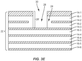
- FIG. 3E is a cross-sectional view of the laminate structure 22 of FIG. 3D after a depth of the fiducial 30 is increased even further into the laminate structure 22.
- portions of the first and second dielectric layers 16-1, 16-2 that were registered with the opening 28 are removed such that the opening 28 is configured to extend to the third metal layer 14-3.
- the shape of the opening 28 is defined by a pattern of the first metal layer 14-1, the first dielectric layer 16-1, and the second dielectric layer 16-2, and the fiducial 30 comprises a surface of the third metal layer 14-3 that is exposed by the opening 28.
- the opening 28 is thereby configured to extend through the opening 24 of the second metal layer 14-2.
- the fiducial 30 is formed in the laminate structure 22 and the fiducial 30 is defined by the opening 28 that extends through the first metal layer 14-1, the first dielectric layer 16-1, and the second metal layer 14-2.
- a width of the opening 28 may define a width of the fiducial 30.
- a sidewall 28' of the opening 28 comprises a portion of the first metal layer 14-1 and a portion of the first dielectric layer 16-1.
- the sidewall 28' may also comprise a portion of the second dielectric layer 16-2.
- the sidewall 28' may also refer to a sidewall of the laminate structure 22 that is within the opening 28 and the sidewall 28' may also be configured to define at least a portion of the fiducial 30.
- the opening 24 in the second metal layer 14-2 is configured with a larger width across the laminate structure 22 than a width of the opening 28.
- the sidewall 28' may be devoid of the second metal layer 14-2.
- the fiducial 30 is configured to extend further into the laminate structure 22, thereby providing even further improved visibility and contrast when viewed from above the laminate structure 22. Additionally, at least some portions of the fiducial 30 are defined by edges of the first metal layer 14-1 at the opening 28, thereby forming a well-defined edge for optical detection equipment.
- a selective removal process may be performed on the laminate structure 22 in certain examples and embodiments.
- the selective removal process may comprise laser drilling where pulsed laser energy from a laser source such as a carbon dioxide (CO 2 ) laser is applied to the laminate structure 22 at the opening 28.
- the laser energy may be configured to be absorbed by and promote ablation of the first and second dielectric layers 16-1, 16-2. Additionally, the laser energy may be configured to have reduced absorption by the metal layers 14-1, 14-3. In this regard, the laser energy may be applied over a wider area of the laminate structure 22 and the shape of the fiducial 30 will be defined by the pattern or opening 28 that extends through the first metal layer 14-1.
- different depths of fiducials 30 may be configured by initially arranging additional openings of various metal layers within the laminate structure 22.
- the third metal layer 14-3 may be formed with an opening similar to the opening 24 of the second metal layer 14-2.
- a laser drilling process may ablate portions of the first, second, and third dielectric layers 16-1 to 16-3 before stopping at the fourth metal layer 14-4.
- Other subtractive removal steps are contemplated, including mechanical drilling or cutting, and etching, among others.
- FIG. 4A is a cross-sectional view of a laminate structure 32 as an example in which every feature of the independent claims is not explicitly recited but which is useful for understanding the invention, that includes a solder mask 34.
- the laminate structure 32 is similar to the laminate structure 22 of FIG. 3D and accordingly includes the metal layers 14-1 - 14-6, the dielectric layers 16-1 - 16-5, the opening 28 that is defined by a pattern of the first metal layer 14-1, and the fiducial 30 as previously described.
- the solder mask 34 may be configured to provide electrical isolation on the top of the laminate structure 32 as well as to provide oxidation protection.
- the solder mask 34 may be configured on the first metal layer 14-1 to form a solder mask opening 36 that is registered with the fiducial 30.
- the solder mask opening 36 is configured with a larger width across the laminate structure 32 than a width of the fiducial 30 across the laminate structure 32. Accordingly, a portion of the first metal layer 14-1 that is closest to the opening 28 may be devoid of the solder mask 34 to provide access to the opening 28 in subsequent processing steps as well as to provide increased visibility of the fiducial 30.
- FIG. 4B is a cross-sectional view of the laminate structure 32 of FIG. 4A after a depth of the fiducial 30 is increased.
- the depth of the fiducial 30 may be increased by a subtractive material process, such as the laser drilling as previously described for FIG. 3E .
- a subtractive material process such as the laser drilling as previously described for FIG. 3E .
- one or more additional layers or coatings may be applied to surfaces of laminate structures as disclosed herein.
- one or more additional layers may include additional dielectric coatings and/or additional metal coatings, among others.
- electrical components or modules on a laminate structure may be coated with one or more metal coatings to form an electromagnetic shield for reducing electromagnetic interference or crosstalk between different ones of the electrical components or modules.
- An electromagnetic shield may include one or more thin metal layers sequentially deposited over a laminate structure to cover a particular electrical component or module.
- An electromagnetic shield may also include one or more metal particles or flecks suspended in a binder.
- fiducials that are provided in the laminate structure may also be coated with the electromagnetic shield coatings. According to configurations of fiducials as disclosed herein, fiducials may be coated with additional layers or coatings and still maintain sufficient visibility and contrast to be viewed and detected with automated processing equipment.
- FIG. 5A is cross-sectional view of a laminate structure 38 that includes a metal coating 40 on the laminate structure 38 as an example in which every feature of the independent claims is not explicitly recited but which is useful for understanding the invention.
- the metal coating 40 may comprise one or more layers or sub-layers that form an electromagnetic shield for electrical components or modules that are mounted in other locations of the laminate structure 38.
- the metal coating 40 may be deposited by one or more combinations of electroless plating, electrolytic plating, other plating processes, sputtering, dispensing, and spraying, among others.
- the metal coating 40 comprises one or more layers of Cu, nickel (Ni), and combinations thereof.
- the metal coating 40 may comprise a first layer of electroless Cu, a second layer of electrolytic Cu, and a third layer of electrolytic Ni to form an electromagnetic shield.
- the metal coating 40 comprises conductive metal particles or flecks that are suspended or filled in an epoxy material or binder to form an electromagnetic shield.
- the epoxy material may be filed with one or more combinations of conductive metal particles or flecks of Cu, silver (Ag), tin/zinc alloys (Sn/Zn), or other conductive materials.
- the laminate structure 38 in FIG. 5A is similar to the laminate structure 22 of FIG.
- the 3E and accordingly includes the metal layers 14-1 to 14-6, the dielectric layers 16-1 to 16-5, the opening 28 that is defined by a pattern of the first metal layer 14-1, and the fiducial 30 as previously described.
- the opening 28 may also be covered by the metal coating 40.
- the metal coating 40 may be configured to extend into the opening 28 and to cover the sidewall 28'.
- the metal coating 40 may be configured to extend into the opening 28 to cover the surface of the third metal layer 14-3 that is exposed by the opening 28.
- the fiducial 30 is defined by the opening 28 and the metal coating 40 is configured to cover one or more surfaces of the laminate structure 38 that are outside of the opening 28 (e.g., top surfaces of the first metal layer 14-1) as well as one or more surfaces of the laminate structure 38 that are within the opening 28 (e.g., the sidewall 28' and a portion of the third metal layer 14-3).
- FIG. 5B is a cross-sectional view of the laminate structure 38 of FIG. 5A for embodiments that include the solder mask 34 as described for FIG. 4A and FIG. 4B .
- the solder mask 34 may be configured as previously described and the metal coating 40 may subsequently be formed on the laminate structure 38 to cover at least a portion of the solder mask 34.
- the metal coating 40 may also be configured to cover portions of the first metal layer 14-1 that are uncovered by the solder mask 34, and the metal coating 40 may also be configured to extend into the opening 28 as previously described.
- the metal coating 40 covers the sidewall 28' of the opening 28 as well as a portion of the third metal layer 14-3 within the opening 28.
- a laminate structure as disclosed herein may be populated with arrays of one or more electronic components that form an array of electronic modules.
- the electronic components are mounted on and electrically connected to one or more of the metal layers of the laminate structure.
- the laminate structure may be diced or singulated along dicing lines or streets that extend between individual ones or groups of electronic modules, thereby forming a plurality of separated electronic modules.
- Fiducials as described herein may be provided at various locations in the laminate structure. In certain embodiments, fiducials are placed to identify the location of the dicing lines for dicing equipment. In certain embodiments, fiducials may also be placed to identify the locations where individual electronic components are to be mounted for placement equipment.
- FIG. 6A is a top view of a representative laminate structure 42 on which a plurality of electronic modules 44 have been mounted to form an array of the electronic modules 44.
- various combinations of one or more electrical components including resistors, capacitors, inductors, resonators, bond wires, and ICs may form each of the electronic modules 44.
- Streets or dicing lines 46 are configured between rows and columns of the electronic modules 44. For simplicity, only a few dicing lines 46 are shown, but it is understood dicing lines 46 can be formed between every column and every row of the electronic modules 44.
- a plurality of fiducials 30 are arranged in the laminate structure 42 as previously described. As illustrated in FIG.
- the plurality of fiducials 30 are configured in areas of the laminate structure 42 that are spaced apart from where the electronic modules 44 are mounted.
- the fiducials 30 are arranged along the perimeter of the laminate structure 42 and the fiducials 30 are configured to be registered with or aligned with the dicing lines 46.
- an automated dicing machine may be configured to detect the location of each fiducial 30 and properly align the machine to cut, saw, break, or otherwise separate the laminate structure 42 along each of the dicing lines 46.
- each of the fiducials 30 may comprise an alignment marker that indicates the location of each dicing line 46 for singulation.
- the dicing lines 46 or streets may comprise a width as measured by a distance between adjacent electronic modules 44 in a range of about 100 microns ( ⁇ m) to about 500 ⁇ m.
- the fiducials 30 are registered with the width of the dicing lines 46.
- the fiducials 30 may comprise a longest dimension across the surface (e.g., diameter for circular fiducials) of the laminate structure 42 that is approximately the same as the width of the dicing lines 46.
- the fiducials 30 may comprise a longest dimension across the surface of the laminate structure 42 that is less than the width of the dicing lines 46.
- the fiducials 30 may comprise a longest dimension across the surface of the laminate structure 42 that is greater than the width of the dicing lines 46.
- the fiducials 30 may be registered with the dicing lines 46 such that a center point of each fiducial 30 is aligned with at least one dicing line 46.
- the longest dimension of the fiducials 30 across the surface of the laminate structure 42 may include a range from about 100 ⁇ m to about 500 ⁇ m, or in a range from about 200 ⁇ m to about 400 ⁇ m, or in a range from about 250 ⁇ m to about 350 ⁇ m.
- the fiducials 30 may be provided in locations that are adjacent to each of the electronic modules 44 to indicate a mounting location for each of the electronic modules 44.
- FIG. 6B is a top view of the laminate structure 42 of FIG. 6A after the metal coating 40 as described for FIG. 5A and FIG. 5B has been formed.
- the metal coating 40 is blanket deposited across the plurality of electronic modules 44 and surfaces of the laminate structure 42 that are uncovered by the plurality of electronic modules 44.
- the metal coating 40 may comprise an electromagnetic shield as previously described. In this manner, each of the electronic modules 44 is coated with an electromagnetic shield that will remain on each of the electronic modules 44 after singulation along each of the dicing lines 46.
- the metal coating 40 may also be configured to coat the fiducials 30.
- the fiducials 30 as disclosed herein are provided with increased visibility and contrast at least partly due to the increased depth in which the fiducials 30 are formed within the laminate structure 42. In this manner, the metal coating 40 may not obscure the fiducials 30, thereby allowing the fiducials 30 to remain visible from the top view with sufficient contrast to be detected by cameras or other detection equipment of automated dicing equipment.
Landscapes
- Engineering & Computer Science (AREA)
- Microelectronics & Electronic Packaging (AREA)
- Manufacturing & Machinery (AREA)
- Physics & Mathematics (AREA)
- Optics & Photonics (AREA)
- Production Of Multi-Layered Print Wiring Board (AREA)
- Shielding Devices Or Components To Electric Or Magnetic Fields (AREA)
- Structure Of Printed Boards (AREA)
- Laminated Bodies (AREA)
Claims (14)
- Vorrichtung, Folgendes umfassend:
eine Laminatstruktur (38), Folgendes umfassend:mehrere Metallschichten (14-1 bis 14-6), die in einer alternierenden Konfiguration mit mehreren dielektrischen Schichten (16-1 bis 16-5) angeordnet sind;eine Bezugsmarke (30), die durch eine Öffnung (28) in der Laminatstruktur definiert ist, wobei sich die Öffnung durch eine erste und eine zweite Metallschicht (14-1, 14-2) der mehreren Metallschichten erstreckt, wobei die erste Metallschicht (14-1) eine oberste Schicht der Laminatstruktur (38) ist; undeine Lötmaske (34) auf einer Oberfläche der ersten Metallschicht, wobei die Lötmaske eine Lötmaskenöffnung (36) ausbildet, die mit der Bezugsmarke ausgerichtet ist;wobei die Vorrichtung weiterhin eine Metallbeschichtung (40) auf der Laminatstruktur umfasst, wobei sich die Metallbeschichtung von der ersten und der zweiten Metallschicht unterscheidet und die Metallbeschichtung auf mindestens einer horizontalen Oberfläche der Laminatstruktur, die sich außerhalb der Öffnung befindet, auf mindestens einer horizontalen Oberfläche der Laminatstruktur, die einen Boden der Öffnung bedeckt, und auf einer Seitenwand (28') der Öffnung angeordnet ist. - Vorrichtung nach Anspruch 1, wobei sich die Öffnung durch mindestens zwei dielektrische Schichten (16-1, 16-2) der mehreren dielektrischen Schichten erstreckt.
- Vorrichtung nach Anspruch 1 oder 2, wobei die mindestens eine horizontale Fläche der Laminatstruktur am Boden der Öffnung durch eine Fläche einer dritten Metallschicht der mehreren Metallschichten definiert ist.
- Vorrichtung nach einem vorhergehenden Anspruch, wobei die Metallbeschichtung eine elektromagnetische Abschirmung umfasst.
- Vorrichtung nach einem vorhergehenden Anspruch, wobei die Lötmaskenöffnung mit einer größeren Breite über die Laminatstruktur als einer Breite der Bezugsmarke über die Laminatstruktur eingerichtet ist.
- Vorrichtung nach einem vorhergehenden Anspruch, wobei die Metallbeschichtung eingerichtet ist, um mindestens einen Abschnitt der Lötmaske zu bedecken.
- Vorrichtung nach einem vorhergehenden Anspruch, wobei ein Abschnitt der Oberfläche der ersten Metallschicht, welcher der Öffnung am nächsten ist, ohne die Lötmaske ist.
- Vorrichtung nach Anspruch 7, wobei die Metallbeschichtung eingerichtet ist, um den Abschnitt der Oberfläche der ersten Metallschicht zu bedecken, welcher der Öffnung am nächsten ist und ohne die Lötmaske ist.
- Vorrichtung nach einem vorhergehenden Anspruch, wobei die Seitenwand der Bezugsmarke einen Abschnitt der ersten Metallschicht und einen Abschnitt der ersten dielektrischen Schicht umfasst.
- Vorrichtung nach Anspruch 9, wobei die Seitenwand der Bezugsmarke ohne die zweite Metallschicht ist.
- Vorrichtung nach einem vorhergehenden Anspruch, wobei die Bezugsmarke einen Ausrichtungsmarker umfasst.
- Vorrichtung nach einem vorhergehenden Anspruch, wobei eine Dicke der ersten Metallschicht größer ist als eine Dicke der zweiten Metallschicht.
- Vorrichtung nach einem vorhergehenden Anspruch, weiterhin umfassend ein elektronisches Modul (44) auf einer Oberfläche der Laminatstruktur, wobei die Bezugsmarke in einem Abschnitt der Laminatstruktur ausgebildet ist, der lateral von dem elektronischen Modul beabstandet ist.
- Vorrichtung nach einem vorhergehenden Anspruch, wobei die Metallbeschichtung mindestens eines von Kupfer und Nickel umfasst.
Applications Claiming Priority (4)
| Application Number | Priority Date | Filing Date | Title |
|---|---|---|---|
| US201962815375P | 2019-03-08 | 2019-03-08 | |
| US16/383,752 US11596058B2 (en) | 2019-03-08 | 2019-04-15 | Fiducials for laminate structures |
| PCT/US2020/021404 WO2020185566A1 (en) | 2019-03-08 | 2020-03-06 | Fiducials for laminate structures |
| EP20717016.8A EP3935924B1 (de) | 2019-03-08 | 2020-03-06 | Bezugsmarker für laminatstrukturen |
Related Parent Applications (2)
| Application Number | Title | Priority Date | Filing Date |
|---|---|---|---|
| EP20717016.8A Division-Into EP3935924B1 (de) | 2019-03-08 | 2020-03-06 | Bezugsmarker für laminatstrukturen |
| EP20717016.8A Division EP3935924B1 (de) | 2019-03-08 | 2020-03-06 | Bezugsmarker für laminatstrukturen |
Publications (3)
| Publication Number | Publication Date |
|---|---|
| EP4243579A2 EP4243579A2 (de) | 2023-09-13 |
| EP4243579A3 EP4243579A3 (de) | 2023-11-29 |
| EP4243579B1 true EP4243579B1 (de) | 2025-01-15 |
Family
ID=72335834
Family Applications (2)
| Application Number | Title | Priority Date | Filing Date |
|---|---|---|---|
| EP20717016.8A Active EP3935924B1 (de) | 2019-03-08 | 2020-03-06 | Bezugsmarker für laminatstrukturen |
| EP23185218.7A Active EP4243579B1 (de) | 2019-03-08 | 2020-03-06 | Bezugsmarken für laminatstrukturen |
Family Applications Before (1)
| Application Number | Title | Priority Date | Filing Date |
|---|---|---|---|
| EP20717016.8A Active EP3935924B1 (de) | 2019-03-08 | 2020-03-06 | Bezugsmarker für laminatstrukturen |
Country Status (5)
| Country | Link |
|---|---|
| US (1) | US11596058B2 (de) |
| EP (2) | EP3935924B1 (de) |
| KR (1) | KR102791592B1 (de) |
| CN (2) | CN119450895A (de) |
| WO (1) | WO2020185566A1 (de) |
Families Citing this family (1)
| Publication number | Priority date | Publication date | Assignee | Title |
|---|---|---|---|---|
| JP7153438B2 (ja) * | 2017-10-26 | 2022-10-14 | 日東電工株式会社 | 基板集合体シート |
Family Cites Families (20)
| Publication number | Priority date | Publication date | Assignee | Title |
|---|---|---|---|---|
| US4916260A (en) * | 1988-10-11 | 1990-04-10 | International Business Machines Corporation | Circuit member for use in multilayered printed circuit board assembly and method of making same |
| GB2258183A (en) | 1991-08-01 | 1993-02-03 | Motorola Inc | Solder mask defined printed circuit board |
| WO1998020534A1 (en) | 1996-11-08 | 1998-05-14 | W.L. Gore & Associates, Inc. | Method for using fiducial schemes to increase nominal registration |
| JPH10294541A (ja) * | 1997-04-16 | 1998-11-04 | Japan Aviation Electron Ind Ltd | 表面自動実装用プリント基板のフェデューシャルマーク構造 |
| US7042004B2 (en) * | 2002-06-21 | 2006-05-09 | Interuniversitair Microelektronica Centrum (Imec) | Method of forming quantum-mechanical memory and computational devices and devices obtained thereof |
| US20060087031A1 (en) | 2004-10-25 | 2006-04-27 | Fujifilm Electronic Imaging Ltd. | Assembly and method |
| US7583834B2 (en) | 2005-03-04 | 2009-09-01 | Eastman Kodak Company | Laser etched fiducials in roll-roll display |
| US8062930B1 (en) | 2005-08-08 | 2011-11-22 | Rf Micro Devices, Inc. | Sub-module conformal electromagnetic interference shield |
| US8359739B2 (en) | 2007-06-27 | 2013-01-29 | Rf Micro Devices, Inc. | Process for manufacturing a module |
| JP2007059627A (ja) | 2005-08-24 | 2007-03-08 | Nitto Denko Corp | Tab用テープキャリアの製造方法 |
| DE102006051597A1 (de) * | 2006-11-02 | 2008-05-08 | Atmel Germany Gmbh | Halbleiteranordnung und Verfahren zur Herstellung einer Halbleiteranordnung |
| US8647517B2 (en) | 2007-07-09 | 2014-02-11 | Nitto Denko Corporation | Producing method of suspension board with circuit |
| US7939369B2 (en) * | 2009-05-14 | 2011-05-10 | International Business Machines Corporation | 3D integration structure and method using bonded metal planes |
| CN101971719B (zh) | 2009-06-04 | 2013-01-16 | 揖斐电株式会社 | 多连片基板的制造方法以及多连片基板 |
| JP2011049316A (ja) | 2009-08-26 | 2011-03-10 | Nitto Denko Corp | 配線回路基板およびその製造方法 |
| JP5739226B2 (ja) * | 2011-05-17 | 2015-06-24 | 株式会社ジャパンディスプレイ | 電子デバイスモジュールの製造方法 |
| KR101269903B1 (ko) | 2011-06-27 | 2013-05-31 | 주식회사 심텍 | 다이스택 패키지 및 제조 방법 |
| US9095083B2 (en) | 2013-11-07 | 2015-07-28 | Unimicron Technology Corp. | Manufacturing method for multi-layer circuit board |
| WO2018236885A1 (en) * | 2017-06-20 | 2018-12-27 | Natcore Technology, Inc. | System and methods for forming foil contact rear emitter solar cells with carrier selective contacts |
| JP2019204894A (ja) * | 2018-05-24 | 2019-11-28 | 東芝メモリ株式会社 | 半導体装置の製造方法および半導体装置 |
-
2019
- 2019-04-15 US US16/383,752 patent/US11596058B2/en active Active
-
2020
- 2020-03-06 CN CN202411679538.XA patent/CN119450895A/zh active Pending
- 2020-03-06 EP EP20717016.8A patent/EP3935924B1/de active Active
- 2020-03-06 WO PCT/US2020/021404 patent/WO2020185566A1/en not_active Ceased
- 2020-03-06 EP EP23185218.7A patent/EP4243579B1/de active Active
- 2020-03-06 CN CN202080034015.3A patent/CN113796166B/zh active Active
- 2020-03-06 KR KR1020217032540A patent/KR102791592B1/ko active Active
Also Published As
| Publication number | Publication date |
|---|---|
| EP3935924B1 (de) | 2024-01-31 |
| KR102791592B1 (ko) | 2025-04-08 |
| EP4243579A2 (de) | 2023-09-13 |
| WO2020185566A1 (en) | 2020-09-17 |
| EP3935924A1 (de) | 2022-01-12 |
| CN113796166B (zh) | 2024-12-03 |
| EP4243579A3 (de) | 2023-11-29 |
| KR20210148173A (ko) | 2021-12-07 |
| US11596058B2 (en) | 2023-02-28 |
| CN113796166A (zh) | 2021-12-14 |
| US20200288567A1 (en) | 2020-09-10 |
| CN119450895A (zh) | 2025-02-14 |
Similar Documents
| Publication | Publication Date | Title |
|---|---|---|
| US9966333B2 (en) | Semiconductor substrate, semiconductor module and method for manufacturing the same | |
| JP5466785B1 (ja) | 回路モジュール及びその製造方法 | |
| US9006580B2 (en) | Method of manufacturing multilayer wiring substrate, and multilayer wiring substrate | |
| US9282626B2 (en) | Printed circuit board and method for manufacturing the same | |
| US4995941A (en) | Method of manufacture interconnect device | |
| KR102267242B1 (ko) | 적층형 전자부품 및 적층형 전자부품의 제조 방법 | |
| WO2011126646A2 (en) | Improved backdrilling of multilayer printed circuit boards | |
| US20090250258A1 (en) | Wiring Substrate, Semiconductor Package, Electronic Instrument, And Wiring Substrate Manufacturing Method | |
| US20200305314A1 (en) | Electromagnetic shields for sub-modules | |
| EP2656703B1 (de) | Leiterplatte und verfahren zu ihrer herstellung | |
| KR101164957B1 (ko) | 인쇄회로기판 및 그 제조방법 | |
| US20060157852A1 (en) | Circuit barrier structure of semiconductor packaging substrate and method for fabricating the same | |
| EP1971194A2 (de) | Anschlusssubstrat und Herstellungsverfahren dafür | |
| EP4243579B1 (de) | Bezugsmarken für laminatstrukturen | |
| US7246434B1 (en) | Method of making a surface mountable PCB module | |
| US11432406B2 (en) | Package substrate | |
| US5843806A (en) | Methods for packaging tab-BGA integrated circuits | |
| US20240347477A1 (en) | Method for forming a shielding layer over a semiconductor package with reduced metal burrs | |
| KR101088030B1 (ko) | 임베디드 인쇄회로기판 및 그 제조방법 | |
| KR20110093407A (ko) | 인쇄회로기판 및 그 제조방법 | |
| TWI842111B (zh) | 多層基板和其製造方法包括及多層基板的電子裝置 | |
| KR20150115346A (ko) | 인쇄회로기판 및 이의 제조 방법 | |
| US20240203896A1 (en) | Semiconductor device package and method of manufacturing the same |
Legal Events
| Date | Code | Title | Description |
|---|---|---|---|
| PUAI | Public reference made under article 153(3) epc to a published international application that has entered the european phase |
Free format text: ORIGINAL CODE: 0009012 |
|
| STAA | Information on the status of an ep patent application or granted ep patent |
Free format text: STATUS: THE APPLICATION HAS BEEN PUBLISHED |
|
| AC | Divisional application: reference to earlier application |
Ref document number: 3935924 Country of ref document: EP Kind code of ref document: P |
|
| AK | Designated contracting states |
Kind code of ref document: A2 Designated state(s): AL AT BE BG CH CY CZ DE DK EE ES FI FR GB GR HR HU IE IS IT LI LT LU LV MC MK MT NL NO PL PT RO RS SE SI SK SM TR |
|
| REG | Reference to a national code |
Ref country code: DE Ref legal event code: R079 Free format text: PREVIOUS MAIN CLASS: H05K0003000000 Ipc: H05K0001020000 Ref document number: 602020045025 Country of ref document: DE |
|
| PUAL | Search report despatched |
Free format text: ORIGINAL CODE: 0009013 |
|
| AK | Designated contracting states |
Kind code of ref document: A3 Designated state(s): AL AT BE BG CH CY CZ DE DK EE ES FI FR GB GR HR HU IE IS IT LI LT LU LV MC MK MT NL NO PL PT RO RS SE SI SK SM TR |
|
| RIC1 | Information provided on ipc code assigned before grant |
Ipc: H05K 3/00 20060101ALN20231024BHEP Ipc: H05K 3/34 20060101ALN20231024BHEP Ipc: H05K 1/02 20060101AFI20231024BHEP |
|
| STAA | Information on the status of an ep patent application or granted ep patent |
Free format text: STATUS: REQUEST FOR EXAMINATION WAS MADE |
|
| 17P | Request for examination filed |
Effective date: 20240524 |
|
| RBV | Designated contracting states (corrected) |
Designated state(s): AL AT BE BG CH CY CZ DE DK EE ES FI FR GB GR HR HU IE IS IT LI LT LU LV MC MK MT NL NO PL PT RO RS SE SI SK SM TR |
|
| GRAP | Despatch of communication of intention to grant a patent |
Free format text: ORIGINAL CODE: EPIDOSNIGR1 |
|
| STAA | Information on the status of an ep patent application or granted ep patent |
Free format text: STATUS: GRANT OF PATENT IS INTENDED |
|
| RIC1 | Information provided on ipc code assigned before grant |
Ipc: H05K 3/00 20060101ALN20240724BHEP Ipc: H05K 3/34 20060101ALN20240724BHEP Ipc: H05K 1/02 20060101AFI20240724BHEP |
|
| INTG | Intention to grant announced |
Effective date: 20240801 |
|
| RIN1 | Information on inventor provided before grant (corrected) |
Inventor name: CULLER, JAMES EDWIN JR. Inventor name: PARKER, STEPHEN CRAIG Inventor name: ORLOWSKI, JOHN AUGUST |
|
| GRAS | Grant fee paid |
Free format text: ORIGINAL CODE: EPIDOSNIGR3 |
|
| GRAA | (expected) grant |
Free format text: ORIGINAL CODE: 0009210 |
|
| STAA | Information on the status of an ep patent application or granted ep patent |
Free format text: STATUS: THE PATENT HAS BEEN GRANTED |
|
| AC | Divisional application: reference to earlier application |
Ref document number: 3935924 Country of ref document: EP Kind code of ref document: P |
|
| AK | Designated contracting states |
Kind code of ref document: B1 Designated state(s): AL AT BE BG CH CY CZ DE DK EE ES FI FR GB GR HR HU IE IS IT LI LT LU LV MC MK MT NL NO PL PT RO RS SE SI SK SM TR |
|
| REG | Reference to a national code |
Ref country code: CH Ref legal event code: EP Ref country code: GB Ref legal event code: FG4D |
|
| REG | Reference to a national code |
Ref country code: DE Ref legal event code: R096 Ref document number: 602020045025 Country of ref document: DE |
|
| REG | Reference to a national code |
Ref country code: IE Ref legal event code: FG4D |
|
| REG | Reference to a national code |
Ref country code: NL Ref legal event code: MP Effective date: 20250115 |
|
| PG25 | Lapsed in a contracting state [announced via postgrant information from national office to epo] |
Ref country code: NL Free format text: LAPSE BECAUSE OF FAILURE TO SUBMIT A TRANSLATION OF THE DESCRIPTION OR TO PAY THE FEE WITHIN THE PRESCRIBED TIME-LIMIT Effective date: 20250115 |
|
| PG25 | Lapsed in a contracting state [announced via postgrant information from national office to epo] |
Ref country code: RS Free format text: LAPSE BECAUSE OF FAILURE TO SUBMIT A TRANSLATION OF THE DESCRIPTION OR TO PAY THE FEE WITHIN THE PRESCRIBED TIME-LIMIT Effective date: 20250415 |
|
| PG25 | Lapsed in a contracting state [announced via postgrant information from national office to epo] |
Ref country code: FI Free format text: LAPSE BECAUSE OF FAILURE TO SUBMIT A TRANSLATION OF THE DESCRIPTION OR TO PAY THE FEE WITHIN THE PRESCRIBED TIME-LIMIT Effective date: 20250115 |
|
| PG25 | Lapsed in a contracting state [announced via postgrant information from national office to epo] |
Ref country code: PL Free format text: LAPSE BECAUSE OF FAILURE TO SUBMIT A TRANSLATION OF THE DESCRIPTION OR TO PAY THE FEE WITHIN THE PRESCRIBED TIME-LIMIT Effective date: 20250115 |
|
| PG25 | Lapsed in a contracting state [announced via postgrant information from national office to epo] |
Ref country code: ES Free format text: LAPSE BECAUSE OF FAILURE TO SUBMIT A TRANSLATION OF THE DESCRIPTION OR TO PAY THE FEE WITHIN THE PRESCRIBED TIME-LIMIT Effective date: 20250115 |
|
| REG | Reference to a national code |
Ref country code: LT Ref legal event code: MG9D |
|
| PG25 | Lapsed in a contracting state [announced via postgrant information from national office to epo] |
Ref country code: IS Free format text: LAPSE BECAUSE OF FAILURE TO SUBMIT A TRANSLATION OF THE DESCRIPTION OR TO PAY THE FEE WITHIN THE PRESCRIBED TIME-LIMIT Effective date: 20250515 Ref country code: NO Free format text: LAPSE BECAUSE OF FAILURE TO SUBMIT A TRANSLATION OF THE DESCRIPTION OR TO PAY THE FEE WITHIN THE PRESCRIBED TIME-LIMIT Effective date: 20250415 |
|
| REG | Reference to a national code |
Ref country code: AT Ref legal event code: MK05 Ref document number: 1760669 Country of ref document: AT Kind code of ref document: T Effective date: 20250115 |
|
| PG25 | Lapsed in a contracting state [announced via postgrant information from national office to epo] |
Ref country code: HR Free format text: LAPSE BECAUSE OF FAILURE TO SUBMIT A TRANSLATION OF THE DESCRIPTION OR TO PAY THE FEE WITHIN THE PRESCRIBED TIME-LIMIT Effective date: 20250115 |
|
| PG25 | Lapsed in a contracting state [announced via postgrant information from national office to epo] |
Ref country code: LV Free format text: LAPSE BECAUSE OF FAILURE TO SUBMIT A TRANSLATION OF THE DESCRIPTION OR TO PAY THE FEE WITHIN THE PRESCRIBED TIME-LIMIT Effective date: 20250115 Ref country code: PT Free format text: LAPSE BECAUSE OF FAILURE TO SUBMIT A TRANSLATION OF THE DESCRIPTION OR TO PAY THE FEE WITHIN THE PRESCRIBED TIME-LIMIT Effective date: 20250515 |
|
| PG25 | Lapsed in a contracting state [announced via postgrant information from national office to epo] |
Ref country code: BG Free format text: LAPSE BECAUSE OF FAILURE TO SUBMIT A TRANSLATION OF THE DESCRIPTION OR TO PAY THE FEE WITHIN THE PRESCRIBED TIME-LIMIT Effective date: 20250115 Ref country code: GR Free format text: LAPSE BECAUSE OF FAILURE TO SUBMIT A TRANSLATION OF THE DESCRIPTION OR TO PAY THE FEE WITHIN THE PRESCRIBED TIME-LIMIT Effective date: 20250416 |
|
| PG25 | Lapsed in a contracting state [announced via postgrant information from national office to epo] |
Ref country code: AT Free format text: LAPSE BECAUSE OF FAILURE TO SUBMIT A TRANSLATION OF THE DESCRIPTION OR TO PAY THE FEE WITHIN THE PRESCRIBED TIME-LIMIT Effective date: 20250115 |
|
| PG25 | Lapsed in a contracting state [announced via postgrant information from national office to epo] |
Ref country code: SE Free format text: LAPSE BECAUSE OF FAILURE TO SUBMIT A TRANSLATION OF THE DESCRIPTION OR TO PAY THE FEE WITHIN THE PRESCRIBED TIME-LIMIT Effective date: 20250115 |
|
| P01 | Opt-out of the competence of the unified patent court (upc) registered |
Free format text: CASE NUMBER: UPC_APP_2776_4243579/2025 Effective date: 20250807 |
|
| PG25 | Lapsed in a contracting state [announced via postgrant information from national office to epo] |
Ref country code: SM Free format text: LAPSE BECAUSE OF FAILURE TO SUBMIT A TRANSLATION OF THE DESCRIPTION OR TO PAY THE FEE WITHIN THE PRESCRIBED TIME-LIMIT Effective date: 20250115 |
|
| PG25 | Lapsed in a contracting state [announced via postgrant information from national office to epo] |
Ref country code: DK Free format text: LAPSE BECAUSE OF FAILURE TO SUBMIT A TRANSLATION OF THE DESCRIPTION OR TO PAY THE FEE WITHIN THE PRESCRIBED TIME-LIMIT Effective date: 20250115 |
|
| PG25 | Lapsed in a contracting state [announced via postgrant information from national office to epo] |
Ref country code: MC Free format text: LAPSE BECAUSE OF FAILURE TO SUBMIT A TRANSLATION OF THE DESCRIPTION OR TO PAY THE FEE WITHIN THE PRESCRIBED TIME-LIMIT Effective date: 20250115 |
|
| PG25 | Lapsed in a contracting state [announced via postgrant information from national office to epo] |
Ref country code: IT Free format text: LAPSE BECAUSE OF FAILURE TO SUBMIT A TRANSLATION OF THE DESCRIPTION OR TO PAY THE FEE WITHIN THE PRESCRIBED TIME-LIMIT Effective date: 20250115 |
|
| REG | Reference to a national code |
Ref country code: DE Ref legal event code: R097 Ref document number: 602020045025 Country of ref document: DE |
|
| PG25 | Lapsed in a contracting state [announced via postgrant information from national office to epo] |
Ref country code: EE Free format text: LAPSE BECAUSE OF FAILURE TO SUBMIT A TRANSLATION OF THE DESCRIPTION OR TO PAY THE FEE WITHIN THE PRESCRIBED TIME-LIMIT Effective date: 20250115 Ref country code: CZ Free format text: LAPSE BECAUSE OF FAILURE TO SUBMIT A TRANSLATION OF THE DESCRIPTION OR TO PAY THE FEE WITHIN THE PRESCRIBED TIME-LIMIT Effective date: 20250115 |
|
| PG25 | Lapsed in a contracting state [announced via postgrant information from national office to epo] |
Ref country code: RO Free format text: LAPSE BECAUSE OF FAILURE TO SUBMIT A TRANSLATION OF THE DESCRIPTION OR TO PAY THE FEE WITHIN THE PRESCRIBED TIME-LIMIT Effective date: 20250115 |
|
| REG | Reference to a national code |
Ref country code: CH Ref legal event code: H13 Free format text: ST27 STATUS EVENT CODE: U-0-0-H10-H13 (AS PROVIDED BY THE NATIONAL OFFICE) Effective date: 20251023 |
|
| PG25 | Lapsed in a contracting state [announced via postgrant information from national office to epo] |
Ref country code: SK Free format text: LAPSE BECAUSE OF FAILURE TO SUBMIT A TRANSLATION OF THE DESCRIPTION OR TO PAY THE FEE WITHIN THE PRESCRIBED TIME-LIMIT Effective date: 20250115 |
|
| PG25 | Lapsed in a contracting state [announced via postgrant information from national office to epo] |
Ref country code: LU Free format text: LAPSE BECAUSE OF NON-PAYMENT OF DUE FEES Effective date: 20250306 |
|
| PLBE | No opposition filed within time limit |
Free format text: ORIGINAL CODE: 0009261 |
|
| STAA | Information on the status of an ep patent application or granted ep patent |
Free format text: STATUS: NO OPPOSITION FILED WITHIN TIME LIMIT |
|
| REG | Reference to a national code |
Ref country code: BE Ref legal event code: MM Effective date: 20250331 |
|
| 26N | No opposition filed |
Effective date: 20251016 |
|
| GBPC | Gb: european patent ceased through non-payment of renewal fee |
Effective date: 20250415 |
|
| PG25 | Lapsed in a contracting state [announced via postgrant information from national office to epo] |
Ref country code: GB Free format text: LAPSE BECAUSE OF NON-PAYMENT OF DUE FEES Effective date: 20250415 |
|
| PG25 | Lapsed in a contracting state [announced via postgrant information from national office to epo] |
Ref country code: FR Free format text: LAPSE BECAUSE OF NON-PAYMENT OF DUE FEES Effective date: 20250315 |
|
| PG25 | Lapsed in a contracting state [announced via postgrant information from national office to epo] |
Ref country code: BE Free format text: LAPSE BECAUSE OF NON-PAYMENT OF DUE FEES Effective date: 20250331 |
|
| PG25 | Lapsed in a contracting state [announced via postgrant information from national office to epo] |
Ref country code: CH Free format text: LAPSE BECAUSE OF NON-PAYMENT OF DUE FEES Effective date: 20250331 |
|
| PG25 | Lapsed in a contracting state [announced via postgrant information from national office to epo] |
Ref country code: IE Free format text: LAPSE BECAUSE OF NON-PAYMENT OF DUE FEES Effective date: 20250306 |
|
| PGFP | Annual fee paid to national office [announced via postgrant information from national office to epo] |
Ref country code: DE Payment date: 20260219 Year of fee payment: 7 |