EP4240130B1 - Organische lichtemittierende vorrichtung und elektronische vorrichtung damit - Google Patents
Organische lichtemittierende vorrichtung und elektronische vorrichtung damit Download PDFInfo
- Publication number
- EP4240130B1 EP4240130B1 EP23182925.0A EP23182925A EP4240130B1 EP 4240130 B1 EP4240130 B1 EP 4240130B1 EP 23182925 A EP23182925 A EP 23182925A EP 4240130 B1 EP4240130 B1 EP 4240130B1
- Authority
- EP
- European Patent Office
- Prior art keywords
- group
- substituted
- unsubstituted
- layer
- compound
- Prior art date
- Legal status (The legal status is an assumption and is not a legal conclusion. Google has not performed a legal analysis and makes no representation as to the accuracy of the status listed.)
- Active
Links
Images

Classifications
-
- C—CHEMISTRY; METALLURGY
- C09—DYES; PAINTS; POLISHES; NATURAL RESINS; ADHESIVES; COMPOSITIONS NOT OTHERWISE PROVIDED FOR; APPLICATIONS OF MATERIALS NOT OTHERWISE PROVIDED FOR
- C09K—MATERIALS FOR MISCELLANEOUS APPLICATIONS, NOT PROVIDED FOR ELSEWHERE
- C09K11/00—Luminescent materials, e.g. electroluminescent or chemiluminescent
- C09K11/06—Luminescent materials, e.g. electroluminescent or chemiluminescent containing organic luminescent materials
-
- H—ELECTRICITY
- H10—SEMICONDUCTOR DEVICES; ELECTRIC SOLID-STATE DEVICES NOT OTHERWISE PROVIDED FOR
- H10K—ORGANIC ELECTRIC SOLID-STATE DEVICES
- H10K85/00—Organic materials used in the body or electrodes of devices covered by this subclass
- H10K85/60—Organic compounds having low molecular weight
- H10K85/631—Amine compounds having at least two aryl rest on at least one amine-nitrogen atom, e.g. triphenylamine
- H10K85/633—Amine compounds having at least two aryl rest on at least one amine-nitrogen atom, e.g. triphenylamine comprising polycyclic condensed aromatic hydrocarbons as substituents on the nitrogen atom
-
- C—CHEMISTRY; METALLURGY
- C07—ORGANIC CHEMISTRY
- C07F—ACYCLIC, CARBOCYCLIC OR HETEROCYCLIC COMPOUNDS CONTAINING ELEMENTS OTHER THAN CARBON, HYDROGEN, HALOGEN, OXYGEN, NITROGEN, SULFUR, SELENIUM OR TELLURIUM
- C07F15/00—Compounds containing elements of Groups 8, 9, 10 or 18 of the Periodic Table
- C07F15/0006—Compounds containing elements of Groups 8, 9, 10 or 18 of the Periodic Table compounds of the platinum group
- C07F15/0086—Platinum compounds
-
- C—CHEMISTRY; METALLURGY
- C07—ORGANIC CHEMISTRY
- C07F—ACYCLIC, CARBOCYCLIC OR HETEROCYCLIC COMPOUNDS CONTAINING ELEMENTS OTHER THAN CARBON, HYDROGEN, HALOGEN, OXYGEN, NITROGEN, SULFUR, SELENIUM OR TELLURIUM
- C07F7/00—Compounds containing elements of Groups 4 or 14 of the Periodic Table
- C07F7/02—Silicon compounds
- C07F7/08—Compounds having one or more C—Si linkages
- C07F7/0803—Compounds with Si-C or Si-Si linkages
- C07F7/081—Compounds with Si-C or Si-Si linkages comprising at least one atom selected from the elements N, O, halogen, S, Se or Te
- C07F7/0812—Compounds with Si-C or Si-Si linkages comprising at least one atom selected from the elements N, O, halogen, S, Se or Te comprising a heterocyclic ring
- C07F7/0814—Compounds with Si-C or Si-Si linkages comprising at least one atom selected from the elements N, O, halogen, S, Se or Te comprising a heterocyclic ring said ring is substituted at a C ring atom by Si
-
- C—CHEMISTRY; METALLURGY
- C07—ORGANIC CHEMISTRY
- C07F—ACYCLIC, CARBOCYCLIC OR HETEROCYCLIC COMPOUNDS CONTAINING ELEMENTS OTHER THAN CARBON, HYDROGEN, HALOGEN, OXYGEN, NITROGEN, SULFUR, SELENIUM OR TELLURIUM
- C07F7/00—Compounds containing elements of Groups 4 or 14 of the Periodic Table
- C07F7/02—Silicon compounds
- C07F7/08—Compounds having one or more C—Si linkages
- C07F7/0803—Compounds with Si-C or Si-Si linkages
- C07F7/081—Compounds with Si-C or Si-Si linkages comprising at least one atom selected from the elements N, O, halogen, S, Se or Te
- C07F7/0812—Compounds with Si-C or Si-Si linkages comprising at least one atom selected from the elements N, O, halogen, S, Se or Te comprising a heterocyclic ring
- C07F7/0816—Compounds with Si-C or Si-Si linkages comprising at least one atom selected from the elements N, O, halogen, S, Se or Te comprising a heterocyclic ring said ring comprising Si as a ring atom
-
- H—ELECTRICITY
- H10—SEMICONDUCTOR DEVICES; ELECTRIC SOLID-STATE DEVICES NOT OTHERWISE PROVIDED FOR
- H10K—ORGANIC ELECTRIC SOLID-STATE DEVICES
- H10K50/00—Organic light-emitting devices
- H10K50/10—OLEDs or polymer light-emitting diodes [PLED]
- H10K50/11—OLEDs or polymer light-emitting diodes [PLED] characterised by the electroluminescent [EL] layers
- H10K50/12—OLEDs or polymer light-emitting diodes [PLED] characterised by the electroluminescent [EL] layers comprising dopants
-
- H—ELECTRICITY
- H10—SEMICONDUCTOR DEVICES; ELECTRIC SOLID-STATE DEVICES NOT OTHERWISE PROVIDED FOR
- H10K—ORGANIC ELECTRIC SOLID-STATE DEVICES
- H10K50/00—Organic light-emitting devices
- H10K50/80—Constructional details
- H10K50/84—Passivation; Containers; Encapsulations
- H10K50/842—Containers
- H10K50/8426—Peripheral sealing arrangements, e.g. adhesives, sealants
-
- H—ELECTRICITY
- H10—SEMICONDUCTOR DEVICES; ELECTRIC SOLID-STATE DEVICES NOT OTHERWISE PROVIDED FOR
- H10K—ORGANIC ELECTRIC SOLID-STATE DEVICES
- H10K50/00—Organic light-emitting devices
- H10K50/80—Constructional details
- H10K50/84—Passivation; Containers; Encapsulations
- H10K50/844—Encapsulations
-
- H—ELECTRICITY
- H10—SEMICONDUCTOR DEVICES; ELECTRIC SOLID-STATE DEVICES NOT OTHERWISE PROVIDED FOR
- H10K—ORGANIC ELECTRIC SOLID-STATE DEVICES
- H10K59/00—Integrated devices, or assemblies of multiple devices, comprising at least one organic light-emitting element covered by group H10K50/00
-
- H—ELECTRICITY
- H10—SEMICONDUCTOR DEVICES; ELECTRIC SOLID-STATE DEVICES NOT OTHERWISE PROVIDED FOR
- H10K—ORGANIC ELECTRIC SOLID-STATE DEVICES
- H10K85/00—Organic materials used in the body or electrodes of devices covered by this subclass
- H10K85/30—Coordination compounds
-
- H—ELECTRICITY
- H10—SEMICONDUCTOR DEVICES; ELECTRIC SOLID-STATE DEVICES NOT OTHERWISE PROVIDED FOR
- H10K—ORGANIC ELECTRIC SOLID-STATE DEVICES
- H10K85/00—Organic materials used in the body or electrodes of devices covered by this subclass
- H10K85/30—Coordination compounds
- H10K85/321—Metal complexes comprising a group IIIA element, e.g. Tris (8-hydroxyquinoline) gallium [Gaq3]
- H10K85/324—Metal complexes comprising a group IIIA element, e.g. Tris (8-hydroxyquinoline) gallium [Gaq3] comprising aluminium, e.g. Alq3
-
- H—ELECTRICITY
- H10—SEMICONDUCTOR DEVICES; ELECTRIC SOLID-STATE DEVICES NOT OTHERWISE PROVIDED FOR
- H10K—ORGANIC ELECTRIC SOLID-STATE DEVICES
- H10K85/00—Organic materials used in the body or electrodes of devices covered by this subclass
- H10K85/30—Coordination compounds
- H10K85/341—Transition metal complexes, e.g. Ru(II)polypyridine complexes
- H10K85/342—Transition metal complexes, e.g. Ru(II)polypyridine complexes comprising iridium
-
- H—ELECTRICITY
- H10—SEMICONDUCTOR DEVICES; ELECTRIC SOLID-STATE DEVICES NOT OTHERWISE PROVIDED FOR
- H10K—ORGANIC ELECTRIC SOLID-STATE DEVICES
- H10K85/00—Organic materials used in the body or electrodes of devices covered by this subclass
- H10K85/30—Coordination compounds
- H10K85/341—Transition metal complexes, e.g. Ru(II)polypyridine complexes
- H10K85/348—Transition metal complexes, e.g. Ru(II)polypyridine complexes comprising osmium
-
- H—ELECTRICITY
- H10—SEMICONDUCTOR DEVICES; ELECTRIC SOLID-STATE DEVICES NOT OTHERWISE PROVIDED FOR
- H10K—ORGANIC ELECTRIC SOLID-STATE DEVICES
- H10K85/00—Organic materials used in the body or electrodes of devices covered by this subclass
- H10K85/40—Organosilicon compounds, e.g. TIPS pentacene
-
- H—ELECTRICITY
- H10—SEMICONDUCTOR DEVICES; ELECTRIC SOLID-STATE DEVICES NOT OTHERWISE PROVIDED FOR
- H10K—ORGANIC ELECTRIC SOLID-STATE DEVICES
- H10K85/00—Organic materials used in the body or electrodes of devices covered by this subclass
- H10K85/60—Organic compounds having low molecular weight
-
- H—ELECTRICITY
- H10—SEMICONDUCTOR DEVICES; ELECTRIC SOLID-STATE DEVICES NOT OTHERWISE PROVIDED FOR
- H10K—ORGANIC ELECTRIC SOLID-STATE DEVICES
- H10K85/00—Organic materials used in the body or electrodes of devices covered by this subclass
- H10K85/60—Organic compounds having low molecular weight
- H10K85/615—Polycyclic condensed aromatic hydrocarbons, e.g. anthracene
-
- H—ELECTRICITY
- H10—SEMICONDUCTOR DEVICES; ELECTRIC SOLID-STATE DEVICES NOT OTHERWISE PROVIDED FOR
- H10K—ORGANIC ELECTRIC SOLID-STATE DEVICES
- H10K85/00—Organic materials used in the body or electrodes of devices covered by this subclass
- H10K85/60—Organic compounds having low molecular weight
- H10K85/615—Polycyclic condensed aromatic hydrocarbons, e.g. anthracene
- H10K85/622—Polycyclic condensed aromatic hydrocarbons, e.g. anthracene containing four rings, e.g. pyrene
-
- H—ELECTRICITY
- H10—SEMICONDUCTOR DEVICES; ELECTRIC SOLID-STATE DEVICES NOT OTHERWISE PROVIDED FOR
- H10K—ORGANIC ELECTRIC SOLID-STATE DEVICES
- H10K85/00—Organic materials used in the body or electrodes of devices covered by this subclass
- H10K85/60—Organic compounds having low molecular weight
- H10K85/615—Polycyclic condensed aromatic hydrocarbons, e.g. anthracene
- H10K85/624—Polycyclic condensed aromatic hydrocarbons, e.g. anthracene containing six or more rings
-
- H—ELECTRICITY
- H10—SEMICONDUCTOR DEVICES; ELECTRIC SOLID-STATE DEVICES NOT OTHERWISE PROVIDED FOR
- H10K—ORGANIC ELECTRIC SOLID-STATE DEVICES
- H10K85/00—Organic materials used in the body or electrodes of devices covered by this subclass
- H10K85/60—Organic compounds having low molecular weight
- H10K85/615—Polycyclic condensed aromatic hydrocarbons, e.g. anthracene
- H10K85/626—Polycyclic condensed aromatic hydrocarbons, e.g. anthracene containing more than one polycyclic condensed aromatic rings, e.g. bis-anthracene
-
- H—ELECTRICITY
- H10—SEMICONDUCTOR DEVICES; ELECTRIC SOLID-STATE DEVICES NOT OTHERWISE PROVIDED FOR
- H10K—ORGANIC ELECTRIC SOLID-STATE DEVICES
- H10K85/00—Organic materials used in the body or electrodes of devices covered by this subclass
- H10K85/60—Organic compounds having low molecular weight
- H10K85/631—Amine compounds having at least two aryl rest on at least one amine-nitrogen atom, e.g. triphenylamine
-
- H—ELECTRICITY
- H10—SEMICONDUCTOR DEVICES; ELECTRIC SOLID-STATE DEVICES NOT OTHERWISE PROVIDED FOR
- H10K—ORGANIC ELECTRIC SOLID-STATE DEVICES
- H10K85/00—Organic materials used in the body or electrodes of devices covered by this subclass
- H10K85/60—Organic compounds having low molecular weight
- H10K85/631—Amine compounds having at least two aryl rest on at least one amine-nitrogen atom, e.g. triphenylamine
- H10K85/636—Amine compounds having at least two aryl rest on at least one amine-nitrogen atom, e.g. triphenylamine comprising heteroaromatic hydrocarbons as substituents on the nitrogen atom
-
- H—ELECTRICITY
- H10—SEMICONDUCTOR DEVICES; ELECTRIC SOLID-STATE DEVICES NOT OTHERWISE PROVIDED FOR
- H10K—ORGANIC ELECTRIC SOLID-STATE DEVICES
- H10K85/00—Organic materials used in the body or electrodes of devices covered by this subclass
- H10K85/60—Organic compounds having low molecular weight
- H10K85/649—Aromatic compounds comprising a hetero atom
- H10K85/654—Aromatic compounds comprising a hetero atom comprising only nitrogen as heteroatom
-
- H—ELECTRICITY
- H10—SEMICONDUCTOR DEVICES; ELECTRIC SOLID-STATE DEVICES NOT OTHERWISE PROVIDED FOR
- H10K—ORGANIC ELECTRIC SOLID-STATE DEVICES
- H10K85/00—Organic materials used in the body or electrodes of devices covered by this subclass
- H10K85/60—Organic compounds having low molecular weight
- H10K85/649—Aromatic compounds comprising a hetero atom
- H10K85/657—Polycyclic condensed heteroaromatic hydrocarbons
- H10K85/6572—Polycyclic condensed heteroaromatic hydrocarbons comprising only nitrogen in the heteroaromatic polycondensed ring system, e.g. phenanthroline or carbazole
-
- H—ELECTRICITY
- H10—SEMICONDUCTOR DEVICES; ELECTRIC SOLID-STATE DEVICES NOT OTHERWISE PROVIDED FOR
- H10K—ORGANIC ELECTRIC SOLID-STATE DEVICES
- H10K85/00—Organic materials used in the body or electrodes of devices covered by this subclass
- H10K85/60—Organic compounds having low molecular weight
- H10K85/649—Aromatic compounds comprising a hetero atom
- H10K85/657—Polycyclic condensed heteroaromatic hydrocarbons
- H10K85/6574—Polycyclic condensed heteroaromatic hydrocarbons comprising only oxygen in the heteroaromatic polycondensed ring system, e.g. cumarine dyes
-
- H—ELECTRICITY
- H10—SEMICONDUCTOR DEVICES; ELECTRIC SOLID-STATE DEVICES NOT OTHERWISE PROVIDED FOR
- H10K—ORGANIC ELECTRIC SOLID-STATE DEVICES
- H10K85/00—Organic materials used in the body or electrodes of devices covered by this subclass
- H10K85/60—Organic compounds having low molecular weight
- H10K85/649—Aromatic compounds comprising a hetero atom
- H10K85/657—Polycyclic condensed heteroaromatic hydrocarbons
- H10K85/6576—Polycyclic condensed heteroaromatic hydrocarbons comprising only sulfur in the heteroaromatic polycondensed ring system, e.g. benzothiophene
-
- H—ELECTRICITY
- H10—SEMICONDUCTOR DEVICES; ELECTRIC SOLID-STATE DEVICES NOT OTHERWISE PROVIDED FOR
- H10K—ORGANIC ELECTRIC SOLID-STATE DEVICES
- H10K2101/00—Properties of the organic materials covered by group H10K85/00
- H10K2101/10—Triplet emission
-
- H—ELECTRICITY
- H10—SEMICONDUCTOR DEVICES; ELECTRIC SOLID-STATE DEVICES NOT OTHERWISE PROVIDED FOR
- H10K—ORGANIC ELECTRIC SOLID-STATE DEVICES
- H10K2101/00—Properties of the organic materials covered by group H10K85/00
- H10K2101/30—Highest occupied molecular orbital [HOMO], lowest unoccupied molecular orbital [LUMO] or Fermi energy values
-
- H—ELECTRICITY
- H10—SEMICONDUCTOR DEVICES; ELECTRIC SOLID-STATE DEVICES NOT OTHERWISE PROVIDED FOR
- H10K—ORGANIC ELECTRIC SOLID-STATE DEVICES
- H10K2101/00—Properties of the organic materials covered by group H10K85/00
- H10K2101/40—Interrelation of parameters between multiple constituent active layers or sublayers, e.g. HOMO values in adjacent layers
-
- H—ELECTRICITY
- H10—SEMICONDUCTOR DEVICES; ELECTRIC SOLID-STATE DEVICES NOT OTHERWISE PROVIDED FOR
- H10K—ORGANIC ELECTRIC SOLID-STATE DEVICES
- H10K2101/00—Properties of the organic materials covered by group H10K85/00
- H10K2101/90—Multiple hosts in the emissive layer
-
- H—ELECTRICITY
- H10—SEMICONDUCTOR DEVICES; ELECTRIC SOLID-STATE DEVICES NOT OTHERWISE PROVIDED FOR
- H10K—ORGANIC ELECTRIC SOLID-STATE DEVICES
- H10K50/00—Organic light-emitting devices
- H10K50/10—OLEDs or polymer light-emitting diodes [PLED]
- H10K50/11—OLEDs or polymer light-emitting diodes [PLED] characterised by the electroluminescent [EL] layers
-
- H—ELECTRICITY
- H10—SEMICONDUCTOR DEVICES; ELECTRIC SOLID-STATE DEVICES NOT OTHERWISE PROVIDED FOR
- H10K—ORGANIC ELECTRIC SOLID-STATE DEVICES
- H10K85/00—Organic materials used in the body or electrodes of devices covered by this subclass
- H10K85/30—Coordination compounds
- H10K85/341—Transition metal complexes, e.g. Ru(II)polypyridine complexes
- H10K85/346—Transition metal complexes, e.g. Ru(II)polypyridine complexes comprising platinum
-
- H—ELECTRICITY
- H10—SEMICONDUCTOR DEVICES; ELECTRIC SOLID-STATE DEVICES NOT OTHERWISE PROVIDED FOR
- H10K—ORGANIC ELECTRIC SOLID-STATE DEVICES
- H10K85/00—Organic materials used in the body or electrodes of devices covered by this subclass
- H10K85/60—Organic compounds having low molecular weight
- H10K85/649—Aromatic compounds comprising a hetero atom
- H10K85/657—Polycyclic condensed heteroaromatic hydrocarbons
Definitions
- One or more aspects of embodiments of the present disclosure relate to an organic light-emitting device and an electronic apparatus including the same.
- OLEDs are self-emission devices that, as compared with devices of the related art, have wide viewing angles, high contrast ratios, short response times, excellent characteristics in terms of brightness, driving voltage, and/or response speed, and produce full-color images.
- OLEDs may include a first electrode located on a substrate, and a hole transport region, an emission layer, an electron transport region, and a second electrode sequentially stacked on the first electrode. Holes provided from the first electrode may move toward the emission layer through the hole transport region, and electrons provided from the second electrode may move toward the emission layer through the electron transport region. Carriers, such as holes and electrons, may then recombine in the emission layer to produce excitons. These excitons transition from an excited state to a ground state to thereby generate light.
- US 2011/291080 A1 relates to an electronic device comprising a substrate, a first electrode, at least one organic functional layer, and a second electrode.
- EP 3435438 A2 relates to an OLED whose emissive layer has a first host and an emitter, where the emitter is a phosphorescent metal complex or a delayed fluorescent emitter, where EH1T, the T1 triplet energy of the first host, is higher than EET, the T1 triplet energy of the emitter, where EET is at least 2.50 eV, where the LUMO energy of the first host is higher than the HOMO energy of the emitter, where the absolute value of the difference between the HOMO energy of the emitter and the LUMO energy of the first host is ⁇ E1, where a ⁇ ⁇ E1 - EET ⁇ b; and where a ⁇ 0.05 eV, and b ⁇ 0.60 eV.
- US 2015/115240 A1 relates to an organic electroluminescent device that includes a light-emitting layer between an anode and a cathode opposite to each other.
- One or more aspects of embodiments of the present disclosure are directed toward an organic light-emitting device having low driving voltage, high efficiency, and long lifespan, and an electronic apparatus including the organic light-emitting device.
- the expression "at least one of a, b or c" indicates only a, only b, only c, both a and b, both a and c, both b and c, all of a, b, and c, or variations thereof. Further, the use of “may” when describing embodiments of the present disclosure refers to “one or more embodiments of the present disclosure.”
- organic layer refers to a single layer and/or all layers between the first electrode and the second electrode of the organic light-emitting device.
- a material included in “the organic layer” is not limited to an organic material.
- FIG. 1 is a schematic cross-sectional view of an organic light-emitting device 10 according to an embodiment.
- the organic light-emitting device 10 includes a first electrode 110, an organic layer 150, and a second electrode 190.
- a substrate may be additionally located under the first electrode 110 or above the second electrode 190.
- the substrate may be a glass substrate and/or a plastic substrate.
- the substrate 100 may be a flexible substrate, and, for example, may include plastics with excellent (or suitable) heat resistance and durability, such as polyimide, polyethylene terephthalate (PET), polycarbonate, polyethylene naphthalate, polyarylate (PAR), polyetherimide, or any combination thereof.
- the first electrode 110 may be formed by, for example, depositing or sputtering a material for forming the first electrode 110 on the substrate.
- a material that has a high work function and can easily inject holes may be used as a material for forming the first electrode 110.
- the first electrode 110 may be a reflective electrode, a semi-transmissive electrode, or a transmissive electrode.
- a material for forming the first electrode 110 may include indium tin oxide (ITO), indium zinc oxide (IZO), tin oxide (SnO 2 ), zinc oxide (ZnO), or any combinations thereof.
- the first electrode 110 when the first electrode 110 is a semi-transmissive electrode or a reflective electrode, magnesium (Mg), silver (Ag), aluminium (Al), aluminium-lithium (Al-Li), calcium (Ca), magnesium-indium (Mg-In), magnesium-silver (Mg-Ag), or any combinations thereof may be used as a material for forming the first electrode 110.
- the organic layer 150 may include, between the first electrode 110 and the second electrode 190, i) two or more emitting units stacked sequentially on the first electrode 110 and ii) charge generation layer(s) located between the two or more emitting units.
- the organic light-emitting device 10 may be a tandem organic light-emitting device.
- the hole transport region may have: i) a single-layered structure including (e.g., consisting of) a single material, ii) a single-layered structure including (e.g., consisting of) a plurality of different materials, or iii) a multi-layered structure including a plurality of layers including different materials.
- the hole transport region may include a hole injection layer, a hole transport layer, an emission auxiliary layer, an electron blocking layer, or any combination thereof.
- the hole transport region may have a multi-layered structure including a hole injection layer/hole transport layer structure, a hole injection layer/hole transport layer/emission auxiliary layer structure, a hole injection layer/emission auxiliary layer structure, a hole transport layer/emission auxiliary layer structure, or a hole injection layer/hole transport layer/electron blocking layer structure, wherein, in each structure, layers are stacked sequentially from the first electrode 110, but embodiments of the present disclosure are not limited thereto.
- the hole transport region may include a compound represented by Formula 201, a compound represented by Formula 202, or any combination thereof:
- the compound represented by Formula 201 and the compound represented by Formula 202 may each include at least one of the groups represented by Formulae CY201 to CY217:
- R 10b and R 10c may each independently be the same as described herein in connection with R 10a
- ring CY 201 to ring CY 204 may each independently be a C 3 -C 20 carbocyclic group or a C 1 -C 20 heterocyclic group.
- at least one hydrogen may be substituted with R 10a .
- ring CY 201 to ring CY 204 may each independently be a benzene group, a naphthalene group, a phenanthrene group, or an anthracene group.
- the compound represented by Formula 201 and the compound represented by Formula 202 may each independently include at least one of the groups represented by Formulae CY201 to CY203.
- the compound represented by Formula 201 may include at least one of the groups represented by Formulae CY201 to CY203 and at least one of the groups represented by Formulae CY204 to CY217.
- xa1 may be 1
- R 201 may be a group represented by one of Formulae CY201 to CY203
- xa2 may be 0
- R 202 may be a group represented by one of Formulae CY204 to CY207.
- the compound represented by Formula 201 and the compound represented by Formula 202 may each independently not include groups represented by Formulae CY201 to CY203.
- the compound represented by Formula 201 and the compound represented by Formula 202 may each independently not include groups represented by Formulae CY201 to CY203, but may each include at least one of the groups represented by Formulae CY204 to CY217.
- the compound represented by Formula 201 and the compound represented by Formula 202 may each independently not include groups represented by Formulae CY201 to CY217.
- the hole transport region may include one of Compounds HT1 to HT44, m-MTDATA, TDATA, 2-TNATA, NPB(NPD), ⁇ -NPB, TPD, Spiro-TPD, Spiro-NPB, methylated-NPB, TAPC, HMTPD, 4,4',4"-tris(N-carbazolyl)triphenylamine (TCTA), polyaniline/dodecylbenzenesulfonic acid (PANI/DBSA), poly(3,4-ethylenedioxythiophene)/poly(4-styrenesulfonate) (PEDOT/PSS), polyaniline/camphor sulfonic acid (PANI/CSA), polyaniline/poly(4-styrenesulfonate) (PANI/PSS), or any combination thereof:
- a thickness of the hole transport region may be in a range of about 50 ⁇ to about 10,000 ⁇ , for example, about 100 ⁇ to about 7,000 ⁇ , about 100 ⁇ to about 5,000 ⁇ , about 100 ⁇ to about 4,000 ⁇ or about 100 ⁇ to about 1,000 ⁇ .
- a thickness of the hole injection layer may be in a range of about 100 ⁇ to about 9,000 ⁇ , for example, about 100 ⁇ to about 7,000 ⁇ , about 100 ⁇ to about 5,000 ⁇ , about 100 ⁇ to about 3,000 ⁇ , about 100 ⁇ to about 2,000 ⁇ , about 100 ⁇ to about 1,000 ⁇ , or about 300 ⁇ to about 500 ⁇ , and a thickness of the hole transport layer may be in a range of about 5 ⁇ to about 2,000 ⁇ , for example, about 10 ⁇ to about 1,500 ⁇ .
- the thicknesses of the hole transport region, the hole injection layer, and the hole transport layer are within the ranges above, satisfactory (or suitable) hole transport characteristics may be obtained without a substantial increase in driving voltage.
- the emission auxiliary layer may increase light-emission efficiency by compensating for an optical resonance distance according to the wavelength of light emitted by the emission layer, and the electron blocking layer may block or reduce the leakage of electrons from the electron transport region.
- a material included in the hole transport region may be included in the emission auxiliary layer and/or the electron blocking layer.
- the hole transport region may include, in addition to the materials described above, a charge-generating material for the improvement of conductive properties.
- the charge-generating material may be homogeneously or non-homogeneously dispersed in the hole transport region (for example, in the form of a single layer including (e.g., consisting of) the charge-generating material).
- the charge-generation material may be, for example, a p-dopant.
- the lowest unoccupied molecular orbital (LUMO) energy level of the p-dopant may be equal to or less than -3.5 eV.
- the p-dopant may include a quinone derivative, a cyano group-containing compound, a compound including Elements EL1 and EL2, or any combination thereof.
- Non-limiting examples of the quinone derivative are TCNQ, F4-TCNQ, and the like, and
- non-limiting examples of the cyano group-containing compound are HAT-CN, a compound represented by Formula 221, and the like:
- Element EL1 may be a metal, a metalloid, or a combination thereof
- Element EL2 may be a non-metal, a metalloid, or a combination thereof.
- Non-limiting examples of the metal are: an alkali metal (for example, lithium (Li), sodium (Na), potassium (K), rubidium (Rb), cesium (Cs), etc.); an alkaline earth metal (for example, beryllium (Be), magnesium (Mg), calcium (Ca), strontium (Sr), barium (Ba), etc.); a transition metal (for example, titanium (Ti), zirconium (Zr), hafnium (Hf), vanadium (V), niobium (Nb), tantalum (Ta), chromium (Cr), molybdenum (Mo), tungsten (W), manganese (Mn), technetium (Tc), rhenium (Re), iron (Fe), ruthenium (Ru), osmium (Os), cobalt (Co), rhodium (Rh), iridium (Ir), nickel (Ni), palladium (Pd), platinum (Pt), copper (Cu), silver (A
- Non-limiting examples of the metalloid are silicon (Si), antimony (Sb), tellurium (Te), and the like.
- Non-limiting examples of the non-metal are oxygen (O), halogen (for example, F, Cl, Br, I, etc.), and the like.
- the compound including Elements EL1 and EL2 may include a metal oxide, a metal halide (for example, metal fluoride, metal chloride, metal bromide, metal iodide, etc.), a metalloid halide (for example, metalloid fluoride, metalloid chloride, metalloid bromide, metalloid iodide, etc.), a metal telluride, or any combination thereof.
- a metal oxide for example, metal fluoride, metal chloride, metal bromide, metal iodide, etc.
- a metalloid halide for example, metalloid fluoride, metalloid chloride, metalloid bromide, metalloid iodide, etc.
- a metal telluride or any combination thereof.
- Non-limiting examples of the transition metal halide are titanium halide (for example, TiF 4 , TiCl 4 , TiBr 4 , TiI 4 , etc.), zirconium halide (for example, ZrF 4 , ZrCl 4 , ZrBr 4 , ZrI 4 , etc.), hafnium halide (for example, HfF 4 , HfCl 4 , HfBr 4 , HfI 4 , etc.), vanadium halide (for example, VF 3 , VCl 3 , VBr 3 , VI 3 , etc.), niobium halide (for example, NbF 3 , NbCl 3 , NbBr 3 , NbI 3 , etc.), tantalum halide (for example, TaF 3 , TaCl 3 , TaBr 3 , TaI 3 , etc.), chromium halide (for example, CrF 3 , CrCl
- Non-limiting examples of the lanthanide metal halide are YbF, YbF 2 , YbF 3 , SmF 3 , YbCl, YbCl 2 , YbCl 3 , SmCl 3 , YbBr, YbBr 2 , YbBr 3 , SmBr 3 , Ybl, YbI 2 , YbI 3 , SmI 3 , and the like.
- Non-limiting examples of the metalloid halide are antimony halide (for example, SbCl 5 , etc.), and the like.
- Non-limiting examples of the metal telluride are alkali metal telluride (for example, Li 2 Te, a Na 2 Te, K 2 Te, Rb 2 Te, Cs 2 Te, etc.), alkaline earth metal telluride (for example, BeTe, MgTe, CaTe, SrTe, BaTe, etc.), transition metal telluride (for example, TiTe 2 , ZrTe 2 , HfTe 2 , V 2 Te 3 , Nb 2 Te 3 , Ta 2 Te 3 , Cr 2 Te 3 , Mo 2 Te 3 , W 2 Te 3 , MnTe, TcTe, ReTe, FeTe, RuTe, OsTe, CoTe, RhTe, IrTe, NiTe, PdTe, PtTe, Cu 2 Te, CuTe, Ag 2 Te, AgTe, Au 2 Te, etc.), post-transition metal telluride (for example, ZnTe, etc.), lanthanide metal
- the emission layer may be patterned into a red emission layer, a green emission layer, and/or a blue emission layer, according to a sub-pixel.
- the emission layer may have a stacked structure of two or more layers of a red emission layer, a green emission layer, and a blue emission layer, in which the two or more layers contact each other or are separated from each other.
- the emission layer may include two or more materials of a red light-emitting material, a green light-emitting material, and a blue light-emitting material, in which the two or more materials are mixed with each other in a single layer to emit white light.
- the emission layer may include a host and a dopant.
- a thickness of the emission layer may be in a range of about 100 ⁇ to about 1,000 ⁇ , for example, about 100 A to about 800 ⁇ , about 150 ⁇ to about 800 ⁇ , about 150 ⁇ to about 700 ⁇ , about 150 ⁇ to about 650 ⁇ , about 200 ⁇ to about 600 ⁇ or about 200 ⁇ to about 400 ⁇ .
- excellent (or improved) light-emission characteristics may be obtained without a substantial increase in driving voltage.
- the host may include a compound represented by Formula 301: Formula 301 [Ar 301 ] xb11 -[(L 301 ) xb1 -R 301 ] xb21 ,
- xb11 in Formula 301 is 2 or more
- two or more of Ar 301 (s) may be linked to each other via a single bond.
- the host may include a compound represented by Formula 301-1, a compound represented by Formula 301-2, or any combination thereof:
- the host may include an alkaline earth metal complex.
- the host may include a Be complex (for example, Compound H55), a Mg complex, a Zn complex, or any combination thereof.
- the host may include one of Compounds H1 to H124, 9,10-di(2-naphthyl)anthracene (ADN), 2-methyl-9,10-bis(naphthalen-2-yl)anthracene (MADN), 9,10-di(2-naphthyl)-2-t-butyl-anthracene (TBADN), 4,4'-bis(N-carbazolyl)-1,1'-biphenyl (CBP), 1,3-di-9-carbazolylbenzene (mCP), 1,3,5-tri(carbazol-9-yl)benzene (TCP), or any combination thereof, but embodiments of the present disclosure are not limited thereto:
- the host includes a first host compound, a second host compound, and a third host compound.
- the first host compound satisfies Conditions 1-1 and 1-2: S 1 H 1 > 3 eV T 1 H 1 > 2.8 eV ,
- S 1 energy of a compound as used herein refers to the lowest excitation singlet energy level of the compound. For example, by preparing, on a quartz substrate of the compound, a sample having a thickness of 1,000 ⁇ and analyzing the obtained absorption spectrum from the sample at room temperature, S 1 energy may be calculated. "Onset S 1 energy” of a compound as used herein may refer to the S 1 energy level of a compound in an onset wavelength.
- T 1 energy of a compound as used herein refers to the lowest excitation triplet energy level of the compound. For example, from a sample having a thickness of 1,000 ⁇ , wherein a compound is deposited on a quartz substrate of the compound, an emission spectrum of the sample may be obtained at a temperature of 77K, the first peak (the peak with the shortest wavelength) of the photoluminescence spectrum may be analyzed, and the T 1 energy may be calculated therefrom.
- “Onset T 1 energy” of a compound as used herein refers to the T 1 energy level of a compound in an onset wavelength.
- the emission layer includes the first host compound satisfying Conditions 1-1 and 1-2, so that a suitably high energy host may be used and the balance of electrons and holes in the emission layer may be also improved, thereby exhibiting low driving voltage, high efficiency, and long lifespan.
- the first host compound and the second host compound may satisfy Condition 2-1, and
- the first host compound and the third host compound may satisfy Condition 2-2: LUMO H 1 ⁇ LUMO H 2 LUMO H 1 ⁇ LUMO H 3 ,
- the first host compound and the second host compound may satisfy Condition 3-1, and
- the first host compound and the third host compound may satisfy Condition 3-2: HOMO H 1 > HOMO H 2 HOMO H 1 > HOMO H 3 ,
- the emission layer may include the first host compound, the second host compound, and the third host compound satisfying Conditions 2-1, 2-2, 3-1, and/or 3-2, so that suitably high energy hosts may be used, and the balance between electrons and holes may be also improved, thereby exhibiting low driving voltage, high efficiency, and long lifespan.
- the first host compound may not form an exciplex with the second host compound.
- the first host compound may not form an exciplex with the third host compound.
- the second host compound may form an exciplex with the third host compound.
- the organic light-emitting device when the host included in the emission layer of the organic light-emitting device is formed of a host compound forming an exciplex, an energy level of a formed exciplex may be relatively low compared to a case using a single host compound. Accordingly, the organic light-emitting device may have a limit to stably (suitably) exhibit low driving voltage, high efficiency, and long lifespan.
- the organic light-emitting device includes the first host compound, so that even when the second host compound and the third host compound form an exciplex, the energy level of all the hosts may be increased, thereby obtaining the organic light-emitting device having low driving voltage, high efficiency, and long lifespan.
- the second host compound may be a hole transport compound not including an electron transport moiety
- the third host compound may be an electron transport compound including an electron transport moiety or a bipolar compound including an electron transport moiety.
- the electron transport moiety may include at least one selected from a pyridine group, a pyrimidine group, a triazine group, a quinoline group, an isoquinoline group, and a quinazoline group.
- the first host compound is one of Compounds A-02 to A-10, and A-12 to A-21:
- Compounds A-01 and A-11 are reference compounds not forming part of the present invention.
- an amount of the first host compounc is in a range of about 0.1 parts by weight to about 20 parts by weight.
- the second host compound may be a compound represented by one of Formulae 311-1 to 311-5:
- the second host compound may be selected from a fluorene-containing compound, a carbazole-containing compound, a diarylamine compound, a triarylamine compound, a dibenzofuran-containing compound, a dibenzothiophene-containing compound, and a dibenzosilole-containing compound.
- a 301 to A 304 may each independently be selected from a benzene group, an indene group, a naphthalene group, an anthracene group, a fluorene group, a phenanthrene group, and a carbazole group.
- a 301 , A 302 , and A 304 may each independently be selected from a benzene group, a naphthalene group, and a phenanthrene group.
- a 301 , A 302 , and A 304 may each be a benzene group or a naphthalene group.
- L 301 to L 305 may each independently be selected from:
- R 301 to R 305 may each independently be selected from:
- Q 31 to Q 33 may each independently be selected from a C 1 -C 10 alkyl group, a C 1 -C 10 alkoxy group, a phenyl group, a biphenyl group, a terphenyl group, and a naphthyl group.
- the third host compound may be an electron transport compound including an electron transport moiety.
- the third host compound may be a compound represented by one of Formulae 312-1 and 312-2:
- the third host compound may be a triazine-containing compound, a triazole-containing compound, an imidazole-containing compound, and/or an oxazine-containing compound.
- the third host compound may be a bipolar compound including an electron transport moiety.
- the third host compound may be a compound represented by Formula 313:
- the third host compound may be a compound represented by one of Formulae 313-1 to 313-6:
- a 31 , A 32 , and A 34 may each independently be selected from a benzene group, an indene group, a naphthalene group, an anthracene group, a fluorene group, a phenanthrene group, a pyridine group, a pyrimidine group, a pyrazine group, a pyridazine group, and a carbazole group.
- a 31 , A 32 , and A 34 may each independently be selected from a benzene group, a naphthalene group, a phenanthrene group, a pyridine group, a pyrimidine group, a pyrazine group, and a pyridazine group.
- a 31 , A 32 , and A 34 may each independently be a benzene group, a naphthalene group, or a phenanthrene group.
- a 31 , A 32 , and A 34 may each independently be a benzene group or a naphthalene group.
- L 321 to L 324 and L 331 to L 336 may each independently be selected from:
- R 321 to R 324 and R 331 to R 336 may each independently be selected from:
- Q 31 to Q 33 may each independently be selected from a C 1 -C 10 alkyl group, a C 1 -C 10 alkoxy group, a phenyl group, a biphenyl group, a terphenyl group, and a naphthyl group.
- Q 301 to Q 303 , Q 321 to Q 323 , and Q 331 to Q 333 may each independently be selected from a C 1 -C 10 alkyl group, a C 1 -C 10 alkoxy group, a phenyl group, a biphenyl group, a terphenyl group, a pentalenyl group, an indenyl group, a naphthyl group, an azulenyl group, a heptalenyl group, an indacenyl group, an acenaphthyl group, a fluorenyl group, a spiro-bifluorenyl group, a benzofluorenyl group, a dibenzofluorenyl group, a phenalenyl group, a phenanthrenyl group, an anthracenyl group, a fluoranthenyl group, a triphenylenyl group, a
- the host includes (e.g., may consist of) the first host compound, the second host compound, and the third host compound.
- the host may further include, in addition to the first host compound, the second host compound, and the third host compound, a host compound such as a compound represented by Formula 301.
- Dopant included in emission layer in organic layer 150 is Dopant included in emission layer in organic layer 150
- the dopant may include a phosphorescent dopant compound, a fluorescent dopant compound, a delayed fluorescence dopant compound, or any combination thereof.
- An amount of the dopant in the emission layer may be in a range of about 0.01 parts by weight to about 15 parts by weight based on 100 parts by weight of the host.
- embodiments of the present disclosure are not limited thereto.
- the phosphorescent dopant compound may include at least one transition metal as a central metal.
- the phosphorescent dopant compound may include a monodentate ligand, a bidentate ligand, a tridentate ligand, a tetradentate ligand, a pentadentate ligand, a hexadentate ligand, or any combination thereof.
- the phosphorescent dopant compound may be electrically neutral.
- the phosphorescent dopant compound may include an organometallic compound represented by Formula 401: Formula 401 M(L 401 ) xc1 (L 402 ) xc2
- X 401 may be nitrogen
- X 402 may be carbon
- each of X 401 and X 402 may be nitrogen.
- two ring A 401 (s) in two or more of L 401 (s) may optionally be linked to each other via T 402 , which is a linking group, or two ring A 402 (s) in two or more of L 401 (s) may optionally be linked to each other via T 403 , which is a linking group (see e.g., Compounds PD1 to PD4 and PD7), wherein T 402 and T 403 may each be the same as described in connection with T 401 .
- L 402 in Formula 401 may be an organic ligand.
- the phosphorescent dopant compound may include, for example, one of Compounds PD1 to PD25 or any combination thereof:
- the fluorescent dopant compound may include an amine group-containing compound, a styryl group-containing compound, or any combination thereof.
- the electron transport region may include a compound represented by Formula 601-1:
- the electron transport region may include one of Compounds ET1 to ET45, 2,9-dimethyl-4,7-diphenyl-1,10-phenanthroline (BCP), 4,7-diphenyl-1,10-phenanthroline (Bphen), Alq 3 , BAlq, TAZ, NTAZ, or any combination thereof:
- a thickness of the electron transport region may be in a range of about 100 ⁇ to about 5000 ⁇ or about 160 ⁇ to about 5,000 ⁇ , for example, about 100 ⁇ to about 4,000 ⁇ or about 100 ⁇ to about 1000 ⁇ .
- a thickness of the buffer layer, the hole blocking layer, and/or the electron control layer may each independently be in a range of about 20 ⁇ to about 1,000 ⁇ , for example, about 20 ⁇ to about 700 ⁇ , about 20 ⁇ to about 500 ⁇ , about 20 ⁇ to about 400 ⁇ , about 30 ⁇ to about 400 ⁇ or about 30 ⁇ to about 300 ⁇
- a thickness of the electron transport layer may be in a range of about 100 ⁇ to about 1,000 ⁇ , for example, about 100 ⁇ to about 700 ⁇ , about 100 ⁇ to about 600 ⁇ , about 150 ⁇ to about 600 ⁇ , about 150 ⁇ to about 500 ⁇ or about 200 ⁇ to
- the electron transport region (for example, the electron transport layer in the electron transport region) may further include, in addition to the materials described above, a metal-containing material.
- the metal-containing material may include an alkali metal complex, an alkaline earth-metal complex, or any combination thereof.
- a metal ion of the alkali metal complex may be a Li ion, a Na ion, a K ion, a Rb ion, or a Cs ion
- a metal ion of the alkaline earth-metal complex may be a Be ion, a Mg ion, a Ca ion, a Sr ion, or a Ba ion.
- the electron injection layer may include an alkali metal, an alkaline earth metal, a rare earth metal, an alkali metal-containing compound, an alkaline earth metal-containing compound, a rare earth metal-containing compound, an alkali metal complex, an alkaline earth-metal complex, a rare earth metal complex, or any combinations thereof.
- the alkali metal-containing compound, the alkaline earth metal-containing compound, and the rare earth metal-containing compound may be oxides and/or halides (for example, fluorides, chlorides, bromides, and/or iodides) of the alkali metal, the alkaline earth metal, and the rare earth metal, a telluride, or any combination thereof.
- oxides and/or halides for example, fluorides, chlorides, bromides, and/or iodides
- the alkali metal-containing compound may be alkali metal oxides (such as Li 2 O, Cs 2 O, and/or K 2 O), alkali metal halides (such as LiF, NaF, CsF, KF, Lil, Nal, Csl, and/or KI), or any combination thereof.
- the alkaline earth metal-containing compound may include an alkaline earth metal compound, such as BaO, SrO, CaO, Ba x Sr 1-x O (where x is a real number satisfying 0 ⁇ x ⁇ 1), Ba x Ca 1-x O (where x is a real number satisfying 0 ⁇ x ⁇ 1), and/or the like.
- the rare earth metal-containing compound may include YbF 3 , ScF 3 , Sc 2 O 3 , Y 2 O 3 , Ce 2 O 3 , GdF 3 , TbF 3 , YbI 3 , ScI 3 , TbI 3 , or any combination thereof.
- the rare earth metal-containing compound may include a lanthanide metal telluride.
- Examples of the lanthanide metal telluride are LaTe, CeTe, PrTe, NdTe, PmTe, SmTe, EuTe, GdTe, TbTe, DyTe, HoTe, ErTe, TmTe, YbTe, LuTe, La 2 Te 3 , Ce 2 Te 3 , Pr 2 Te 3 , Nd 2 Te 3 , Pm 2 Te 3 , Sm 2 Te 3 , EU 2 Te 3 , Gd 2 Te 3 , Tb 2 Te 3 , Dy 2 Te 3 , Ho 2 Te 3 , Er 2 Te 3 , Tm 2 Te 3 , Yb 2 Te 3 , Lu 2 Te 3 , and the like.
- the alkali metal complex, the alkaline earth-metal complex, and the rare earth metal complex may each independently include i) an ion of the alkali metal, the alkaline earth metal, and the rare earth metal, respectively, and ii), as a ligand linked to the metal ion, for example, a hydroxyquinoline, a hydroxyisoquinoline, a hydroxybenzoquinoline, a hydroxyacridine, a hydroxyphenanthridine, a hydroxyphenyloxazole, a hydroxyphenylthiazole, a hydroxydiphenyloxadiazole, a hydroxydiphenylthiadiazole, a hydroxyphenylpyridine, a hydroxyphenyl benzimidazole, a hydroxyphenylbenzothiazole, a bipyridine, a phenanthroline, a cyclopentadiene, or any combination thereof.
- the electron injection layer may include (e.g., may consist of) an alkali metal, an alkaline earth metal, a rare earth metal, an alkali metal-containing compound, an alkaline earth metal-containing compound, a rare earth metal-containing compound, an alkali metal complex, an alkaline earth-metal complex, a rare earth metal complex, or any combination thereof, and/or may further include an organic material (for example, a compound represented by Formula 601).
- the electron injection layer includes (e.g., consists of) i) an alkali metal-containing compound (for example, an alkali metal halide), or ii) a) an alkali metal-containing compound (for example, an alkali metal halide); and b) an alkali metal, alkaline earth metal, a rare earth metal, or any combination thereof.
- the electron injection layer may be a KI:Yb co-deposited layer, a Rbl:Yb co-deposited layer, and/or the like.
- the alkali metal, the alkaline earth metal, the rare earth metal, the alkali metal-containing compound, the alkaline earth metal-containing compound, the rare earth metal-containing compound, the alkali metal complex, the alkaline earth-metal complex, the rare earth metal complex, or any combination thereof may be homogeneously or non-homogeneously dispersed in a matrix including the organic material.
- a thickness of the electron injection layer may be in a range of about 1 ⁇ to about 100 ⁇ , for example, about 3 ⁇ to about 90 ⁇ or about 3 ⁇ to about 20 ⁇ . When the thickness of the electron injection layer is satisfied within the range above, satisfactory (or suitable) electron injection characteristics may be obtained without a substantial increase in driving voltage.
- the organic light-emitting device 10 may include a capping layer located outside the first electrode 110 or outside the second electrode 190.
- the organic light-emitting device 10 may include:
- the first capping layer may be located outside the first electrode 110, and/or the second capping layer may be located outside the second electrode 190.
- the organic light-emitting device 10 may have a structure in which the first capping layer, the first electrode 110, the organic layer 150, and the second electrode 190 are sequentially stacked in this stated order, a structure in which the first electrode 110, the organic layer 150, the second electrode 190, and the second capping layer are sequentially stacked in this stated order, or a structure in which the first capping layer, the first electrode 110, the organic layer 150, the second electrode 190, and the second capping layer are sequentially stacked in this stated order.
- Light generated in the emission layer of the organic layer 150 of the organic light-emitting device 10 may be extracted toward the outside through the first electrode 110 and the first capping layer, each of which may be a semi-transmissive electrode or a transmissive electrode, and/or light generated in the emission layer of the organic layer 150 of the organic light-emitting device 10 may be extracted toward the outside through the second electrode 190 and the second capping layer, each of which may be a semi-transmissive electrode or a transmissive electrode.
- the first capping layer and the second capping layer may increase external luminescence efficiency according to the principle of constructive interference. Accordingly, light extraction efficiency of the organic light-emitting device 10 may be increased, so that luminescence efficiency of the organic light-emitting device 10 may be also improved.
- the first capping layer and the second capping layer may each include a material having a refractive index of equal to or greater than 1.6 (at 589 nm).
- At least one selected from the first capping layer and the second capping layer may each independently include a carbocyclic compound, a heterocyclic compound, an amine group-containing compound, a porphyrine derivative, a phthalocyanine derivative, a naphthalocyanine derivative, an alkali metal complex, an alkaline earth-metal complex, or a combination thereof.
- the carbocyclic compound, the heterocyclic compound, and the amine group-containing compound may each independently be optionally substituted with a substituent containing O, N, S, Se, Si, F, CI, Br, I, or any combination thereof.
- At least one of the first capping layer and the second capping layer may each independently include an amine group-containing compound.
- At least one of the first capping layer and the second capping layer may each independently include a compound represented by Formula 201, a compound represented by Formula 202, or any combination thereof.
- the first area may include a red quantum dot
- the second area may include a green quantum dot
- the third area may not include a quantum dot.
- the quantum dot may be the same as described in the present specification.
- Each of the first area, the second area, and/or the third area may further include a scatterer.
- the thin-film transistor may further include a gate electrode, a gate insulation layer, and/or the like.
- Suitable functional layers may be additionally provided, depending on the use of the electronic apparatus.
- the functional layers are a touch-screen layer, a polarization layer, and/or the like, without limitation.
- the touchscreen layer may be a resistive touchscreen layer, a capacitive touchscreen layer, and/or an infrared touchscreen layer.
- the authentication apparatus may be, for example, a biometric authentication apparatus for authenticating an individual by using biometric information of a biometric body (for example, a finger tip, a pupil, and/or the like).
- the authentication apparatus may further include, in addition to the organic light-emitting device, a biometric information collector.
- the electronic apparatus may be applied to various suitable displays, light sources, lighting apparatuses, personal computers (for example, a mobile personal computer), mobile phones, digital cameras, electronic organizers, electronic dictionaries, electronic game machines, medical instruments (for example, electronic thermometers, sphygmomanometers, blood glucose meters, pulse measurement devices, pulse wave measurement devices, electrocardiogram (ECG) displays, ultrasonic diagnostic devices, or endoscope displays), fish finders, various measuring instruments, meters (for example, meters for a vehicle, an aircraft, and/or a vessel), projectors, and/or the like.
- medical instruments for example, electronic thermometers, sphygmomanometers, blood glucose meters, pulse measurement devices, pulse wave measurement devices, electrocardiogram (ECG) displays, ultrasonic diagnostic devices, or endoscope displays
- fish finders various measuring instruments, meters (for example, meters for a vehicle, an aircraft, and/or a vessel), projectors, and/or the like.
- FIG. 2 is a cross-sectional view showing a light-emitting apparatus according to an embodiment of the present disclosure.
- the light-emitting apparatus of FIG. 2 includes a substrate 100, a thin-film transistor (TFT), a light-emitting device, and an encapsulation portion 300 that seals the light-emitting device.
- TFT thin-film transistor
- the substrate 100 may be a flexible substrate, a glass substrate, and/or a metal substrate.
- a buffer layer 210 may be located on the substrate 100.
- the buffer layer 210 may prevent or reduce penetration of impurities through the substrate 100, and may serve to provide a flat (or suitably flat) surface on the substrate 100.
- a TFT may be located on the buffer layer 210.
- the TFT may include an activation layer 220, a gate electrode 240, a source electrode 260, and a drain electrode 270.
- the activation layer 220 may include an inorganic semiconductor (such as silicon and/or polysilicon), an organic semiconductor, and/or an oxide semiconductor, and may include a source region, a drain region and a channel region.
- an inorganic semiconductor such as silicon and/or polysilicon
- an organic semiconductor such as silicon and/or polysilicon
- an oxide semiconductor such as silicon oxide
- the activation layer 220 may include a source region, a drain region and a channel region.
- An interlayer insulating film 250 may be located on the gate electrode 240.
- the interlayer insulating film 250 may be located between the gate electrode 240 and the source electrode 260, to insulate the gate electrode 240 from the source electrode 260, and between the gate electrode 240 and the drain electrode 270, to insulate the gate electrode 240 from the drain electrode 270.
- the source electrode 260 and the drain electrode 270 may be located on the interlayer insulating film 250.
- the interlayer insulating film 250 and the gate insulating film 230 may be formed to expose a source region and a drain region of the activation layer 220, and the source electrode 260 and the drain electrode 270 may be in contact with the exposed portions of the source region and the drain region of the activation layer 220.
- the TFT may be electrically connected to the organic light-emitting device to drive the organic light-emitting device, and may be covered by a passivation layer 280 for protection.
- the passivation layer 280 may include an inorganic insulating film, an organic insulating film, or a combination thereof.
- An organic light-emitting device may be provided on the passivation layer 280.
- the organic light-emitting device includes a first electrode 110, an organic layer 150, and a second electrode 190.
- the first electrode 110 may be located on the passivation layer 280.
- the passivation layer 280 may expose a certain portion of the drain electrode 270, without completely covering the drain electrode 270, and the first electrode 110 may be connected to the exposed portion of the drain electrode 270.
- the second electrode 190 may be arranged on the organic layer 150, and a capping layer 170 may be additionally formed on the second electrode 190.
- the capping layer 170 may be formed to cover the second electrode 190.
- An encapsulation portion 300 may be located on the capping layer 170.
- the encapsulation portion 300 may be located on the organic light-emitting device to protect the organic light-emitting device from moisture and/or oxygen.
- the encapsulation portion 300 may include an inorganic film (such as silicon nitride (SiNx), silicon oxide (SiOx), indium tin oxide, indium zinc oxide, or any combination thereof), an organic film (such as polyethylene terephthalate, polyethylene naphthalate, polycarbonate, polyimide, polyethylene sulfonate, polyoxymethylene, polyarylate, hexamethyldisiloxane, an acryl-based resin (for example, polymethyl methacrylate, polyacrylic acid, and/or the like), an epoxy-based resion (for example, aliphatic glycidyl ether (AGE) and/or the like), or a combination thereof), or a combination of an inorganic film and an organic film.
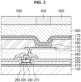
- FIG. 3 is a cross-sectional view showing a light-emitting apparatus according to another embodiment of the present disclosure.
- quantum dots refer to crystals of a semiconductor compound, and may include any material capable of emitting luminescence wavelength of different lengths according to the size of the crystals. Therefore, a material for quantum dots is not limited.
- a diameter of the quantum dot is not particularly limited, but may be, for example, in a range of about 1 nm to about 10 nm.
- Quantum dots arranged in the emission layer including the quantum dots may be synthesized by a wet chemical process, a metal organic chemical vapor deposition process, a molecular beam epitaxy process, or any process similar thereto.
- a precursor material may be added to an organic solvent to grow a quantum dot particle crystal.
- the organic solvent acts as a dispersant naturally coordinated on the surface of the quantum dot crystal, and controls the growth of the crystal.
- MOCVD metal organic chemical vapor deposition
- MBE molecular beam epitaxy
- the growth of quantum dot particles may be suitably controlled.
- the quantum dot may be a Groups III-VI semiconductor compound; a Groups II-VI semiconductor compound; a Groups III-V semiconductor compound; a Groups IV-VI semiconductor compound; a Group IV element or compound; or any combination thereof.
- the Groups III-VI semiconductor compound may include a binary compound, such as In 2 S 3 ; a ternary compound, such as AgInS, AgInS 2 , CulnS, and/or CuInS 2 ; or any combination thereof.
- a binary compound such as In 2 S 3
- a ternary compound such as AgInS, AgInS 2 , CulnS, and/or CuInS 2 ; or any combination thereof.
- the Groups II-VI semiconductor compound may include a binary compound, such as CdSe, CdTe, ZnS, ZnSe, ZnTe, ZnO, HgS, HgSe, HgTe, MgSe, and/or MgS; a ternary compound, such as CdSeS, CdSeTe, CdSTe, ZnSeS, ZnSeTe, ZnSTe, HgSeS, HgSeTe, HgSTe, CdZnS, CdZnSe, CdZnTe, CdHgS, CdHgSe, CdHgTe, HgZnS, HgZnSe, HgZnTe, MgZnSe, and/or MgZnS; a quaternary compound, such as CdZnSeS, CdZnSeTe, CdZnSTe, CdHgSeS,
- the Groups III-V semiconductor compound may include a binary compound, such as GaN, GaP, GaAs, GaSb, AlN, AlP, AlAs, AlSb, InN, InP, InAs, and/or InSb; a ternary compound, such as GaNP, GaNAs, GaNSb, GaPAs, GaPSb, AINP, AlNAs, AlNSb, AlPAs, AlPSb, InGaP, InNP, InNAs, InNSb, InPAs, and/or InPSb; a quaternary compound, such as GaAlNP, GaAINAs, GaAINSb, GaAlPAs, GaAlPSb, GalnNP, GalnNAs, GaInNSb, GalnPAs, GalnPSb, InAlNP, InAlNAs, InAlNSb, InAlPAs, and/or InAlPSb; or any combination thereof.
- a binary compound such as GaN, GaP, GaAs, Ga
- the Groups IV-VI semiconductor compound may include a binary compound, such as SnS, SnSe, SnTe, PbS, PbSe, and/or PbTe; a ternary compound, such as SnSeS, SnSeTe, SnSTe, PbSeS, PbSeTe, PbSTe, SnPbS, SnPbSe, and/or SnPbTe; a quaternary compound, such as SnPbSSe, SnPbSeTe, and/or SnPbSTe; or any combination thereof.
- the Group IV element or compound may include a single element compound, such as Si and/or Ge; a binary compound, such as SiC and/or SiGe; or any combination thereof.
- respective elements included in the binary compound, the ternary compound, or the quaternary compound may exist in particles at uniform concentration or may exist in the same particle in a state in which a concentration distribution is partially different.
- Non-limiting examples of the ⁇ electron-deficient nitrogen-containing C 1 -C 60 cyclic group include a pyrazole group, an imidazole group, a triazole group, an oxazole group, an isoxazole group, an oxadiazole group, a thiazole group, an isothiazole group, a thiadiazole group, a benzopyrazole group, a benzimidazole group, a benzoxazole group, a benzoisoxazole group, a benzothiazole group, a benzisothiazole group, a pyridine group, a pyrimidine group, a pyrazine group, a pyridazine group, a triazine group, a quinoline group, an isoquinoline group, a benzoquinoline group, a benzoisoquinoline group, a quinoxaline group, a benzoquinoxaline group, a quin
- the T1 group may be a cyclopropane group, a cyclobutane group, a cyclopentane group, a cyclohexane group, a cycloheptane group, a cyclooctane group, a cyclobetene group, a cyclopentene group, a cyclopentadiene group, a cyclohexene group, a cyclohexadiene group, a cycloheptene group, an adamantane group, a norbornane group (or, a bicyclo[2.2.1]heptane group), a norbornene group, a bicyclo[1.1.1]pentane group, a bicyclo[2.1.1]hexane group, a bicyclo[2.2.2]octane group, or a benzene group.
- Examples of a monovalent C 3 -C 60 carbocyclic group and a monovalent C 1 -C 60 heterocyclic group are a C 3 -C 10 cycloalkyl group, a C 1 -C 10 heterocycloalkyl group, a C 3 -C 10 cycloalkenyl group, a C 1 -C 10 heterocycloalkenyl group, a C 6 -C 60 aryl group, a C 1 -C 60 heteroaryl group, a monovalent non-aromatic condensed polycyclic group, and a monovalent non-aromatic condensed heteropolycyclic group group; and examples of a divalent C 3 -C 60 carbocyclic group and a divalent C 1 -C 60 heterocyclic group are a C 3 -C 10 cycloalkylene group, a C 1 -C 10 heterocycloalkylene group, a C 3 -C 10 cycloalkenylene group, a C 1 -C 10
- C 2 -C 60 alkynyl group refers to a monovalent hydrocarbon group having at least one carbon-carbon triple bond in the middle and/or at either terminus of a C 2 -C 60 alkyl group, and non-limiting examples thereof include an ethynyl group, and a propynyl group.
- C 2 -C 60 alkynylene group refers to a divalent group having the same structure as the C 2 -C 60 alkynyl group. Corresponding definitions apply to other ranges given for the number of carbon atoms in an alkynyl/alkynylene group.
- C 3 -C 10 cycloalkyl group refers to a monovalent saturated hydrocarbon cyclic group having 3 to 10 carbon atoms, and non-limiting examples thereof are a cyclopropyl group, a cyclobutyl group, a cyclopentyl group, a cyclohexyl group, a cycloheptyl group, a cyclooctyl group, an adamantanyl group, a norbornanyl group, (or a bicyclo[2.2.1]heptyl group), a bicyclo[1.1.1]pentyl group, a bicyclo[2.1.1]hexyl group, and a bicyclo[2.2.2]octyl group.
- C 3 -C 10 cycloalkylene group refers to a divalent group having the same structure as the C 3 -C 10 cycloalkyl group.
- C 1 -C 10 heterocycloalkenyl group refers to a monovalent cyclic group further including at least one heteroatom, other than carbon atoms, as a ring-forming atom, having 1 to 10 carbon atoms, and including at least one carbon-carbon double bond in its ring.
- Non-limiting examples of the C 1 -C 10 heterocycloalkenyl group include a 4,5-dihydro-1,2,3,4-oxatriazolyl group, a 2,3-dihydrofuranyl group, a 2,3-dihydrothiophenyl group, and the like.
- C 1 -C 10 heterocycloalkenylene group refers to a divalent group having the same structure as the C 1 -C 10 heterocycloalkenyl group.
- C 6 -C 60 aryl group refers to a monovalent group having a carbocyclic aromatic system having 6 to 60 carbon atoms.
- Non-limiting examples of the C 6 -C 60 aryl group are a phenyl group, a pentalenyl group, a naphthyl group, an azulenyl group, an indacenyl group, an acenaphthyl group, a phenalenyl group, a phenanthrenyl group, an anthracenyl group, a fluoranthenyl group, a triphenylenyl group, a pyrenyl group, a chrysenyl group, a perylenyl group, a pentaphenyl group, a heptalenyl group, a naphthacenyl group, a picenyl group, a hexacenyl group, a pentaceny
- C 6 -C 60 arylene group refers to a divalent group having the same structure as the C 6 -C 60 aryl group.
- the respective two or more rings may be condensed to each other.
- Corresponding definitions apply to other ranges given for the number of carbon atoms in an aryl/arylene group.
- C 1 -C 60 heteroaryl group refers to a monovalent group having an aromatic system that further includes at least one heteroatom, other than carbon atoms, as a ring-forming atom and has 1 to 60 carbon atoms.
- Non-limiting examples of the C 1 -C 60 heteroaryl group are a pyridinyl group, a pyrimidinyl group, a pyrazinyl group, a pyridazinyl group, a triazinyl group, a quinolinyl group, a benzoquinolinyl group, an isoquinolinyl group, a benzoisoquinolinyl group, a quinoxalinyl group, a benzoquinoxalinyl group, a quinazolinyl group, a benzoquinazolinyl group, a cinnolinyl group, a phenanthrolinyl group, a phthalazinyl group, a naphthyridinyl group, or the like.
- C 1 -C 60 heteroarylene group refers to a divalent group having the same structure as the C 1 -C 60 heteroaryl group.
- the respective two or more rings may be condensed with each other.
- Corresponding definitions apply to other ranges given for the number of carbon atoms in an heteroaryl/heteroarylene group.
- the term "monovalent non-aromatic condensed polycyclic group” as used herein refers to a monovalent group having two or more rings condensed with each other, only carbon atoms as ring-forming atoms (for example, having 8 to 60 carbon atoms), and no aromaticity in its entire molecular structure (e.g., the molecular structure as a whole is non-aromatic).
- Non-limiting examples of the monovalent non-aromatic condensed polycyclic group are an indenyl group, a fluorenyl group, a spiro-bifluorenyl group, a benzofluorenyl group, an indenophenanthrenyl group, and an indenoanthracenyl group.
- divalent non-aromatic condensed polycyclic group refers to a divalent group having the same structure as the monovalent non-aromatic condensed polycyclic group.
- non-aromatic condensed heteropolycyclic group refers to a monovalent group having two or more rings condensed with each other, further including at least one heteroatom, other than carbon atoms (for example, having 1 to 60 carbon atoms), as a ring-forming atom, and having non-aromaticity in its entire molecular structure (e.g., the molecular structure as a whole is non-aromatic).
- Non-limiting examples of the monovalent non-aromatic condensed heteropolycyclic group are a pyrrolyl group, a thiophenyl group, a furanyl group, an indolyl group, a benzoindolyl group, a naphthoindolyl group, an isoindolyl group, a benzoisoindolyl group, a naphthoisoindolyl group, a benzosilolyl group, a benzothiophenyl group, a benzofuranyl group, a carbazolyl group, a dibenzosilolyl group, a dibenzothiophenyl group, a dibenzofuranyl group, an azacarbazolyl group, an azafluorenyl group, an azadibenzosilolyl group, an azadibenzothiophenyl group, an azadibenzofuranyl group, a
- C 6 -C 60 aryloxy group refers to a monovalent group represented by -OA 102 (wherein A 102 is the C 6 -C 60 aryl group), and the term “C 6 -C 60 arylthio group” as used herein refers to a monovalent group represented by -SA 103 (wherein A 103 is the C 6 -C 60 aryl group).
- -OA 102 the C 6 -C 60 aryl group
- C 6 -C 60 arylthio group refers to a monovalent group represented by -SA 103 (wherein A 103 is the C 6 -C 60 aryl group).
- Corresponding definitions apply to other ranges given for the number of carbon atoms in an aryloxy group and an arylthio group.
- R 10a as used herein may be:
- Q 1 to Q 3 , Q 11 to Q 13 , Q 21 to Q 23 , and Q 31 to Q 33 may each independently be: hydrogen; deuterium; -F; -Cl; -Br; -I; a hydroxyl group; a cyano group; a nitro group; a C 1 -C 60 ( e.g . C 1 -C 20 ) alkyl group; a C 2 -C 60 ( e.g. C 2 -C 20 ) alkenyl group; a C 2 -C 60 ( e.g. C 2 -C 20 ) alkynyl group; a C 1 -C 60 ( e.g.
- C 1 -C 20 alkoxy group
- a C 3 -C 60 e.g. C 3 -C 30
- carbocyclic group or a C 1 -C 60 e.g. C 1 -C 20 ) heterocyclic group, each independently unsubstituted or substituted with deuterium, -F, a cyano group, a C 1 -C 60 ( e.g . C 1 -C 20 ) alkyl group, a C 1 -C 60 ( e.g. C 1 -C 20 ) alkoxy group, a phenyl group, a biphenyl group, or any combination thereof.
- heteroatom refers to any atom except a carbon atom.
- heteroatom examples include O, S, N, P, Si, B, Ge, Se, or any combination thereof.
- Ph refers to a phenyl group
- Me refers to a methyl group
- Et refers to an ethyl group
- ter-Bu refers to a tert-butyl group
- OMe refers to a methoxy group
- biphenyl group refers to "a phenyl group substituted with a phenyl group.”
- the "biphenyl group” may be a substituted phenyl group having a C 6 -C 60 aryl group as a substituent.
- terphenyl group refers to "a phenyl group substituted with a biphenyl group.”
- the "terphenyl group” may be a substituted phenyl group having, as a substituent, a C 6 -C 60 aryl group substituted with a C 6 -C 60 aryl group.
- Example 1 is a reference Example not forming part of the present invention.
- An ITO glass substrate was cut to a size of 50 mm x 50 mm x 0.5 mm, sonicated with isopropyl alcohol and pure water each for 5 minutes, and then cleaned by exposure to ultraviolet rays and ozone for 30 minutes. Then, the ITO glass substrate was provided to a vacuum deposition apparatus.
- a suitable material NPB for hole injection was vacuum-deposited on the ITO glass substrate to form a hole injection layer having a thickness of 400 ⁇
- a hole transport material mCP was vacuum-deposited on the hole injection layer to form a hole transport layer having a thickness of 10 ⁇ .
- Compound A-01 On the hole transport layer, Compound A-01, co-hosts of Host 1 and Host 2 that form an exciplex, and dopant PHD were co-deposited (wherein a weight ratio of A-01:Host 1:Host 2:PHD was 10:140:140:10) to form an emission layer having a thickness of 300 ⁇ .
- ETL1 and Liq (at a weight ratio of 5:5) were deposited on the emission layer to form an electron transport layer having a thickness of 300 ⁇ , and Al was deposited on the electron transport layer to form an Al electrode (i.e., a cathode electrode) having a thickness of 1,200 ⁇ .
- HT28 was deposited on the Al electrode to form a capping layer having a thickness of 700 ⁇ , thereby completing the manufacture of an organic light-emitting device.
- Examples 2 to 8 and Comparative Examples 1 to 4 , Examples 3 and 7 are reference Examples not forming part of the present invention.
- HOMO energy levels were measured by cyclovoltametry (CV), and LUMO energy levels were measured through a UV-measured band gap.
- S1 is measured from a photoluminescent spectrum
- T1 is measured from a low-temperature photoluminescent spectrum. Results measured therefrom are recorded as shown in Table 1.
- HT1 which is a hole transport compound, had a HOMO energy level of 5.11 eV.
- the organic light-emitting devices according to one or more embodiments of the present disclosure had low driving voltage and excellent characteristics in terms of luminescence efficiency, external quantum efficiency, and lifespan.
- the organic light-emitting devices of Examples 2, 4-6, 8 had excellent luminescence efficiency and/or excellent lifespan characteristics compared to those of the organic light-emitting devices of Comparative Examples 1 to 4.
- the organic light-emitting devices of Examples 2, 4-6, 8 were suitable for emitting blue light, unlike the organic light-emitting devices of Comparative Examples 2 and 3.
- an organic light-emitting device may have low driving voltage, high efficiency, and long lifespan.
- any numerical range recited herein is intended to include all sub-ranges of the same numerical precision subsumed within the recited range.
- a range of "1.0 to 10.0" is intended to include all subranges between (and including) the recited minimum value of 10 and the recited maximum value of 100, that is, having a minimum value equal to or greater than 1.0 and a maximum value equal to or less than 10.0, such as, for example, 2.4 to 7.6.
- Any maximum numerical limitation recited herein is intended to include all lower numerical limitations subsumed therein and any minimum numerical limitation recited in this specification is intended to include all higher numerical limitations subsumed therein.
Landscapes
- Chemical & Material Sciences (AREA)
- Engineering & Computer Science (AREA)
- Materials Engineering (AREA)
- Physics & Mathematics (AREA)
- Spectroscopy & Molecular Physics (AREA)
- Organic Chemistry (AREA)
- Inorganic Chemistry (AREA)
- Crystallography & Structural Chemistry (AREA)
- Optics & Photonics (AREA)
- Electroluminescent Light Sources (AREA)
Claims (11)
- Organische lichtemittierende Vorrichtung, Folgendes umfassend:eine erste Elektrode (110);eine zweite Elektrode (190), die der ersten Elektrode zugewandt ist; undeine organische Schicht (150) zwischen der ersten Elektrode und der zweiten Elektrode und umfassend eine Emissionsschicht,wobei:die Emissionsschicht einen Wirt und ein Dotiermittel umfasst,der Wirt eine erste Wirtsverbindung, eine zweite Wirtsverbindung und eine dritte Wirtsverbindung umfasst, unddie erste Wirtsverbindung die Bedingungen 1-1 und 1-2 erfüllt:

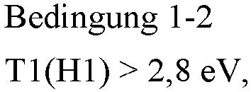 wobei in den Bedingungen 1-1 und 1-2S1(H1) einen Singlett-Energiepegel mit der niedrigsten Anregung der ersten Wirtsverbindung angibt, undT1(H1) einen Triplett-Energiepegel mit der niedrigsten Anregung der ersten Wirtsverbindung angibt, und dadurch gekennzeichnet, dassdie erste Wirtsverbindung ausgewählt ist aus den Verbindungen A-02 bis A-10 und A-12 bis A-21: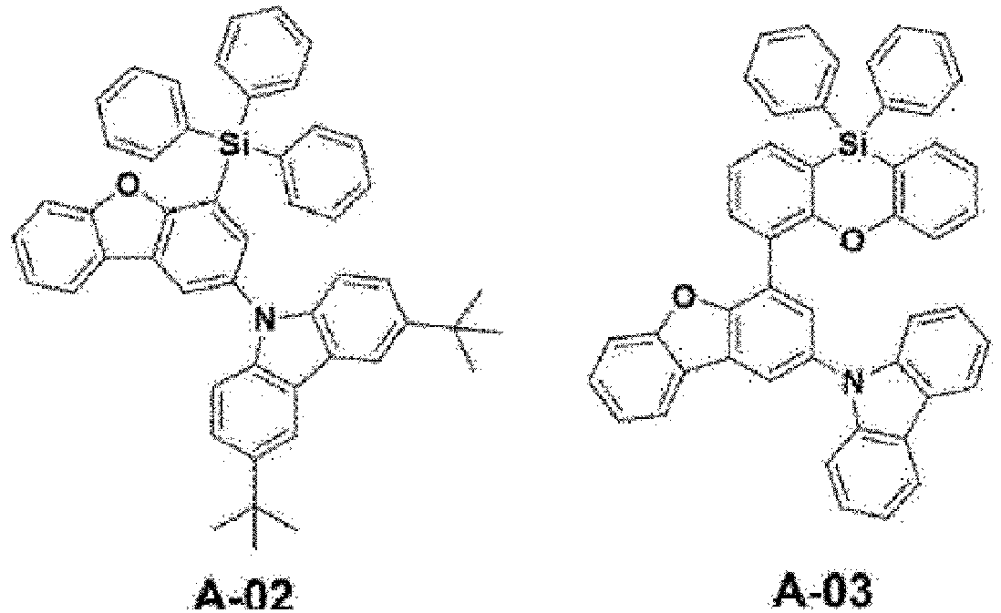


- Organische lichtemittierende Vorrichtung nach Anspruch 1, wobei die erste Wirtsverbindung und die zweite Wirtsverbindung die Bedingung 2-1 erfüllen, unddie erste Wirtsverbindung und die dritte Wirtsverbindung die Bedingung 2-2 erfüllen:

 LUMO (H1) einen Energiepegel des niedrigsten unbesetzten Molekülorbitals (LUMO) der ersten Wirtsverbindung angibt,LUMO (H2) einen LUMO-Energiepegel der zweiten Wirtsverbindung angibt, undLUMO (H3) einen LUMO-Energiepegel der dritten Wirtsverbindung angibt.
 - Organische lichtemittierende Vorrichtung nach Anspruch 1 oder Anspruch 2, wobei eine Menge der ersten Wirtsverbindung in einem Bereich von etwa 0,1 Gewichtsteilen bis etwa 20 Gewichtsteilen liegt, bezogen auf 100 Gewichtsteile des Wirts.
- Organische lichtemittierende Vorrichtung nach einem der Ansprüche 1 bis 3, wobei:(i) die erste Wirtsverbindung keinen Exciplex mit der zweiten Wirtsverbindung bildet, und
die erste Wirtsverbindung keinen Exciplex mit der dritten Wirtsverbindung bildet; und/oder(ii) die zweite Wirtsverbindung und die dritte Wirtsverbindung in der Emissionsschicht einen Exciplex bilden. - Organische lichtemittierende Vorrichtung nach einem der Ansprüche 1 bis 4, wobei die zweite Wirtsverbindung eine Lochtransportverbindung ist, die keine Elektronentransporteinheit einschließt, und
die dritte Wirtsverbindung eine Elektronentransportverbindung, die eine Elektronentransporteinheit umfasst, oder eine bipolare Verbindung, die eine Elektronentransporteinheit umfasst, ist. - Organische lichtemittierende Vorrichtung nach einem der Ansprüche 1 bis 5, wobei die zweite Wirtsverbindung durch die Formeln 311-1 bis 311-5 dargestellt ist:


wobei in den Formeln 311-1 bis 311-5Ar301 eine substituierte oder unsubstituierte carbocyclische C5-C60-Gruppe oder eine substituierte oder unsubstituierte heterocyclische C1-C60-Gruppe ist,xb11 1, 2 oder 3 ist,A301 bis A304 jeweils unabhängig aus einer Benzolgruppe, einer Naphthalingruppe, einer Phenanthrengruppe, einer Fluoranthengruppe, einer Triphenylengruppe, einer Pyrengruppe, einer Chrysengruppe, einer Indengruppe, einer Fluorengruppe, einer Spirobifluorengruppe, einer Benzofluorengruppe, einer Dibenzofluorengruppe, einer Indolgruppe, einer Carbazolgruppe, einer Benzocarbazolgruppe, einer Dibenzocarbazolgruppe, einer Furangruppe, einer Benzofurangruppe, einer Dibenzofurangruppe, einer Naphthofurangruppe, einer Benzonaphthofurangruppe, einer Dinaphthofurangruppe, einer Thiophengruppe, einer Benzothiophengruppe, einer Dibenzothiophengruppe, einer Naphthothiophengruppe, einer Benzonaphthothiophengruppe und einer Dinaphthothiophengruppe ausgewählt sind,X301 O, S, N-[(L304)xb4-R304], C[(L304)xb4-R304][(L305)xb5-R305] oder Si[(L304)xb4-R304][(L305)xb5-R305] ist,X302, Y301 und Y302 jeweils unabhängig eine Einfachbindung, O, S, N-[(L305)xb5-R305], C[(L304)xb4-R304][(L305)xb5-R305], Si[(L304)xb4-R304][(L305)xb5-R305] oder S(=O)2 sind,xb21 bis xb24 jeweils unabhängig 0, 1 oder 2 sind,L301 bis L306 jeweils unabhängig aus einer substituierten oder unsubstituierten C3-C10-Cycloalkylengruppe, einer substituierten oder unsubstituierten C1-C10-Heterocycloalkylengruppe, einer substituierten oder unsubstituierten C3-C10-Cycloalkenylengruppe, einer substituierten oder unsubstituierten C1-C10-Heterocycloalkenylengruppe, einer substituierten oder unsubstituierten C6-C60-Arylengruppe, einer substituierten oder unsubstituierten C1-C60-Heteroarylengruppe, einer substituierten oder unsubstituierten zweiwertigen nicht-aromatischen kondensierten polycyclischen Gruppe und einer substituierten oder unsubstituierten zweiwertigen nicht-aromatischen kondensierten heteropolycyclischen Gruppe ausgewählt sind,xb1 bis xb5 jeweils unabhängig eine ganze Zahl von 0 bis 5 sind,xb6 eine ganze Zahl von 1 bis 5 ist,R301 bis R305 jeweils unabhängig aus Deuterium, -F, -Cl, -Br, -I, einer Hydroxylgruppe, einer Cyanogruppe, einer Nitrogruppe, einer Amidinogruppe, einer Hydrazinogruppe, einer Hydrazonogruppe, einer substituierten oder unsubstituierten C1-C60-Alkylgruppe, einer substituierten oder unsubstituierten C2-C60-Alkenylgruppe, einer substituierten oder unsubstituierten C2-C60-Alkinylgruppe, einer substituierten oder unsubstituierten C1-C60-Alkoxygruppe, einer substituierten oder unsubstituierten C3-C10-Cycloalkylgruppe, einer substituierten oder unsubstituierten C1-C10-Heterocycloalkylgruppe, einer substituierten oder unsubstituierten C3-C10-Cycloalkenylgruppe, einer substituierten oder unsubstituierten C1-C10-Heterocycloalkenylgruppe, einer substituierten oder unsubstituierten C6-C60-Arylgruppe, einer substituierten oder unsubstituierten C6-C60-Aryloxygruppe, einer substituierten oder unsubstituierten C6-C60-Arylthiogruppe, einer substituierten oder unsubstituierten C1-C60-Heteroarylgruppe, einer substituierten oder unsubstituierten einwertigen nicht-aromatischen kondensierten polycyclischen Gruppe, einer substituierten oder unsubstituierten einwertigen nicht-aromatischen kondensierten heteropolycyclischen Gruppe, -Si(Q301)(Q302)(Q303), -N(Q301)(Q302), -B(Q301)(Q302), -C(=O)(Q301), -S(=O)2(Q301) und -P(=O)(Q301)(Q302) ausgewählt sind,R311 bis R314 jeweils unabhängig aus Wasserstoff, Deuterium, -F, -Cl, -Br, -I, einer Hydroxylgruppe, einer Cyanogruppe, einer Nitrogruppe, einer Amidinogruppe, einer Hydrazinogruppe, einer Hydrazonogruppe, einer C1-C20-Alkylgruppe, einer C1-C20-Alkoxygruppe, einer Phenylgruppe, einer Biphenylgruppe, einer Terphenylgruppe, einer Naphthylgruppe, -Si(Q301)(Q302)(Q303), -N(Q301)(Q302), -B(Q301)(Q302), -C(=O)(Q301), -S(=O)2(Q301) und -P(=O)(Q301)(Q302) ausgewählt sind, undQ301 bis Q303 jeweils unabhängig aus Wasserstoff, Deuterium, -F, -Cl, -Br, -I, einer Hydroxylgruppe, einer Cyanogruppe, einer Nitrogruppe, einer Amidinogruppe, einer Hydrazinogruppe, einer Hydrazonogruppe, einer C1-C60-Alkylgruppe, einer C2-C60-Alkenylgruppe, einer C2-C60-Alkinylgruppe, einer C1-C60-Alkoxygruppe, einer C3-C10-Cycloalkylgruppe, einer C1-C10-Heterocycloalkylgruppe, einer C3-C10-Cycloalkenylgruppe, einer C1-C10-Heterocycloalkenylgruppe, einer C6-C60-Arylgruppe, einer C6-C60-Aryloxygruppe, einer C6-C60-Arylthiogruppe, einer C1-C60-Heteroarylgruppe, einer C1-C60-Heteroaryloxygruppe, einer C1-C60-Heteroarylthiogruppe, einer einwertigen nicht-aromatischen kondensierten polycyclischen Gruppe, einer einwertigen nicht-aromatischen kondensierten heteropolycyclischen Gruppe, einer Biphenylgruppe und einer Terphenylgruppe ausgewählt sind. - Organische lichtemittierende Vorrichtung nach einem der Ansprüche 1 bis 6, wobei die dritte Wirtsverbindung durch die Formel 312-1, 312-2 oder 313 dargestellt ist:

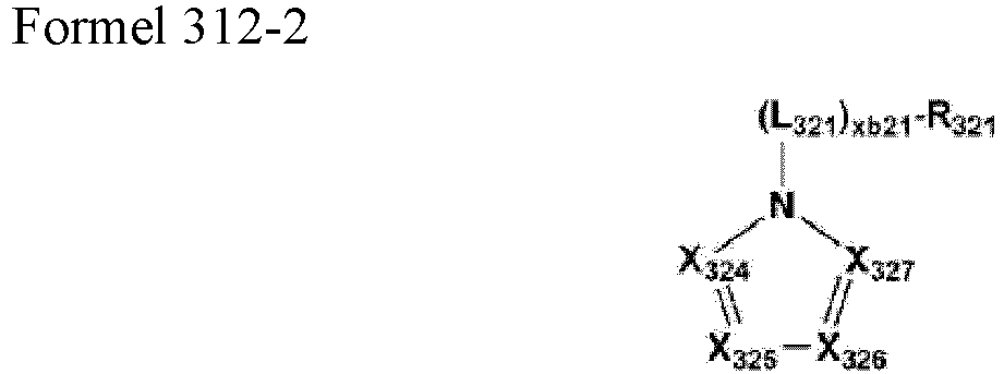


wobei in den Formeln 312-1 und 312-2X321 bis X327 jeweils unabhängig N oder C[(L324)xb24-R324] sind,xb21 bis xb24 jeweils unabhängig eine ganze Zahl von 0 bis 5 sind,L321 bis L324 jeweils unabhängig aus einer substituierten oder unsubstituierten C3-C10-Cycloalkylengruppe, einer substituierten oder unsubstituierten C1-C10-Heterocycloalkylengruppe, einer substituierten oder unsubstituierten C3-C10-Cycloalkenylengruppe, einer substituierten oder unsubstituierten C1-C10-Heterocycloalkenylengruppe, einer substituierten oder unsubstituierten C6-C60-Arylengruppe, einer substituierten oder unsubstituierten C1-C60-Heteroarylengruppe, einer substituierten oder unsubstituierten zweiwertigen nicht-aromatischen kondensierten polycyclischen Gruppe und einer substituierten oder unsubstituierten zweiwertigen nicht-aromatischen kondensierten heteropolycyclischen Gruppe ausgewählt sind,R321 bis R324 jeweils unabhängig aus Wasserstoff, Deuterium, -F, -Cl, -Br, -I, einer Hydroxylgruppe, einer Cyanogruppe, einer Nitrogruppe, einer Amidinogruppe, einer Hydrazinogruppe, einer Hydrazonogruppe, einer substituierten oder unsubstituierten C1-C60-Alkylgruppe, einer substituierten oder unsubstituierten C2-C60-Alkenylgruppe, einer substituierten oder unsubstituierten C2-C60-Alkinylgruppe, einer substituierten oder unsubstituierten C1-C60-Alkoxygruppe, einer substituierten oder unsubstituierten C3-C10-Cycloalkylgruppe, einer substituierten oder unsubstituierten C1-C10-Heterocycloalkylgruppe, einer substituierten oder unsubstituierten C3-C10-Cycloalkenylgruppe, einer substituierten oder unsubstituierten C1-C10-Heterocycloalkenylgruppe, einer substituierten oder unsubstituierten C6-C60-Arylgruppe, einer substituierten oder unsubstituierten C6-C60-Aryloxygruppe, einer substituierten oder unsubstituierten C6-C60-Arylthiogruppe, einer substituierten oder unsubstituierten C1-C60-Heteroarylgruppe, einer substituierten oder unsubstituierten einwertigen nicht-aromatischen kondensierten polycyclischen Gruppe, einer substituierten oder unsubstituierten einwertigen nicht-aromatischen kondensierten heteropolycyclischen Gruppe, -Si(Q321)(Q322)(Q323), -N(Q321)(Q322), -B(Q321)(Q322), -C(=O)(Q321), -S(=O)2(Q321) und -P(=O)(Q321)(Q322) ausgewählt sind,benachbarte zwei oder mehr R321 bis R324 optional miteinander verknüpft sind, um eine substituierte oder unsubstituierte carbocyclische C3-C60-Gruppe oder eine substituierte oder unsubstituierte heterocyclische C1-C60-Gruppe zu bilden,Q321 bis Q323 jeweils unabhängig aus Wasserstoff, Deuterium, -F, -Cl, -Br, -I, einer Hydroxylgruppe, einer Cyanogruppe, einer Nitrogruppe, einer Amidinogruppe, einer Hydrazinogruppe, einer Hydrazonogruppe, einer C1-C60-Alkylgruppe, einer C2-C60-Alkenylgruppe, einer C2-C60-Alkinylgruppe, einer C1-C60-Alkoxygruppe, einer C3-C10-Cycloalkylgruppe, einer C1-C10-Heterocycloalkylgruppe, einer C3-C10-Cycloalkenylgruppe, einer C1-C10-Heterocycloalkenylgruppe, einer C6-C60-Arylgruppe, einer C6-C60-Aryloxygruppe, einer C6-C60-Arylthiogruppe, einer C1-C60-Heteroarylgruppe, einer C1-C60-Heteroaryloxygruppe, einer C1-C60-Heteroarylthiogruppe, einer einwertigen nicht-aromatischen kondensierten polycyclischen Gruppe, einer einwertigen nicht-aromatischen kondensierten heteropolycyclischen Gruppe, einer Biphenylgruppe und einer Terphenylgruppe ausgewählt sind,in Formel 313A31, A32 und A34 jeweils unabhängig aus einer carbocyclischen C5-C60-Gruppe und einer heterocyclischen C1-C30-Gruppe ausgewählt sind,A33 eine Gruppe ist, die durch die Formel 313A dargestellt ist,X31 aus N-[(L335)xb35-(R335)], O, S, Se, C[(L335)xb35-(R335)][(L336)xb36-(R336)] und Si[(L335)xb35-(R335)][(L336)xb36-(R336)] ausgewählt ist,xb31 bis xb36 jeweils unabhängig eine ganze Zahl von 0 bis 5 sind,L331 bis L336 jeweils unabhängig aus einer substituierten oder unsubstituierten C3-C10-Cycloalkylengruppe, einer substituierten oder unsubstituierten C1-C10-Heterocycloalkylengruppe, einer substituierten oder unsubstituierten C3-C10-Cycloalkenylengruppe, einer substituierten oder unsubstituierten C1-C10-Heterocycloalkenylengruppe, einer substituierten oder unsubstituierten C6-C60-Arylengruppe, einer substituierten oder unsubstituierten C1-C60-Heteroarylengruppe, einer substituierten oder unsubstituierten zweiwertigen nicht-aromatischen kondensierten polycyclischen Gruppe und einer substituierten oder unsubstituierten zweiwertigen nicht-aromatischen kondensierten heteropolycyclischen Gruppe ausgewählt sind,R331 bis R336 jeweils unabhängig aus Wasserstoff, Deuterium, -F, -Cl, -Br, -I, einer Hydroxylgruppe, einer Cyanogruppe, einer Nitrogruppe, einer Amidinogruppe, einer Hydrazinogruppe, einer Hydrazonogruppe, einer substituierten oder unsubstituierten C1-C60-Alkylgruppe, einer substituierten oder unsubstituierten C2-C60-Alkenylgruppe, einer substituierten oder unsubstituierten C2-C60-Alkinylgruppe, einer substituierten oder unsubstituierten C1-C60-Alkoxygruppe, einer substituierten oder unsubstituierten C3-C10-Cycloalkylgruppe, einer substituierten oder unsubstituierten C1-C10-Heterocycloalkylgruppe, einer substituierten oder unsubstituierten C3-C10-Cycloalkenylgruppe, einer substituierten oder unsubstituierten C1-C10-Heterocycloalkenylgruppe, einer substituierten oder unsubstituierten C6-C60-Arylgruppe, einer substituierten oder unsubstituierten C6-C60-Aryloxygruppe, einer substituierten oder unsubstituierten C6-C60-Arylthiogruppe, einer substituierten oder unsubstituierten C1-C60-Heteroarylgruppe, einer substituierten oder unsubstituierten einwertigen nicht-aromatischen kondensierten polycyclischen Gruppe, einer substituierten oder unsubstituierten einwertigen nicht-aromatischen kondensierten heteropolycyclischen Gruppe, -Si(Q331)(Q332)(Q333), -N(Q331)(Q332), -B(Q331)(Q332), -C(=O)(Q331), -S(=O)2(Q331) und -P(=O)(Q331)(Q332) ausgewählt sind,xb42 bis xb44 jeweils unabhängig eine ganze Zahl von 0 bis 10 sind, undQ331 bis Q333 jeweils unabhängig aus Wasserstoff, Deuterium, -F, -Cl, -Br, -I, einer Hydroxylgruppe, einer Cyanogruppe, einer Nitrogruppe, einer Amidinogruppe, einer Hydrazinogruppe, einer Hydrazonogruppe, einer C1-C60-Alkylgruppe, einer C2-C60-Alkenylgruppe, einer C2-C60-Alkinylgruppe, einer C1-C60-Alkoxygruppe, einer C3-C10-Cycloalkylgruppe, einer C1-C10-Heterocycloalkylgruppe, einer C3-C10-Cycloalkenylgruppe, einer C1-C10-Heterocycloalkenylgruppe, einer C6-C60-Arylgruppe, einer C6-C60-Aryloxygruppe, einer C6-C60-Arylthiogruppe, einer C1-C60-Heteroarylgruppe, einer C1-C60-Heteroaryloxygruppe, einer C1-C60-Heteroarylthiogruppe, einer einwertigen nicht-aromatischen kondensierten polycyclischen Gruppe, einer einwertigen nicht-aromatischen kondensierten heteropolycyclischen Gruppe, einer Biphenylgruppe und einer Terphenylgruppe ausgewählt sind. - Organische lichtemittierende Vorrichtung nach einem der Ansprüche 1 bis 7, wobei:(i) die organische lichtemittierende Vorrichtung ferner eine Deckschicht auf der zweiten Elektrode umfasst, und
die Deckschicht einen Brechungsindex von 1,6 oder mehr aufweist; und/oder(ii) das Dotiermittel eine phosphoreszierende Dotiermittelverbindung, eine fluoreszierende Dotiermittelverbindung, eine Dotiermittelverbindung mit verzögerter Fluoreszenz oder eine beliebige Kombination davon umfasst; und/oder(iii) die Emissionsschicht dazu dient, blaues Licht mit einer maximalen Lumineszenzwellenlänge, die gleich oder größer als etwa 410 nm und gleich oder kleiner als etwa 490 nm ist, zu emittieren. - Organische lichtemittierende Vorrichtung nach einem der Ansprüche 1 bis 8, wobei die erste Elektrode eine Anode ist,die zweite Elektrode eine Kathode ist,die organische Schicht ferner eine Lochtransportregion zwischen der ersten Elektrode und der Emissionsschicht und eine Elektronentransportregion zwischen der Emissionsschicht und der zweiten Elektrode umfasst;die Lochtransportregion eine Lochinjektionsschicht, eine Lochtransportschicht, eine Emissionshilfsschicht, eine Elektronenblockierschicht oder eine beliebige Kombination davon umfasst, unddie Elektronentransportregion eine Pufferschicht, eine Lochblockierschicht, eine Elektronentransportschicht, eine Elektroneninjektionsschicht oder eine beliebige Kombination davon umfasst, optional wobei die Elektronentransportregion ein metallhaltiges Material umfasst.
- Elektronisches Gerät, umfassend eine organische lichtemittierende Vorrichtung nach einem der Ansprüche 1 bis 9.
- Elektronisches Gerät nach Anspruch 10, wobei:(i) das elektronische Gerät ferner einen Abdichtungsabschnitt umfasst, um die organische lichtemittierende Vorrichtung abzudichten, und
der Abdichtungsabschnitt eine Dünnschicht-Einkapselungsschicht ist, die mindestens eine organische Schicht und/oder mindestens eine anorganische Schicht umfasst; und/oder(ii) das elektronische Gerät ferner einen Dünnschichttransistor umfasst,der Dünnschichttransistor eine Source-Elektrode und eine Drain-Elektrode umfasst, unddie erste Elektrode der organischen lichtemittierenden Vorrichtung mit der Source-Elektrode oder der Drain-Elektrode des Dünnschichttransistors elektrisch verbunden ist.
Applications Claiming Priority (2)
| Application Number | Priority Date | Filing Date | Title |
|---|---|---|---|
| KR1020200059969A KR102797538B1 (ko) | 2020-05-19 | 2020-05-19 | 유기 발광 소자 및 이를 포함한 전자 장치 |
| EP21174464.4A EP3913699B1 (de) | 2020-05-19 | 2021-05-18 | Organische lichtemittierende vorrichtung und elektronische einrichtung damit |
Related Parent Applications (2)
| Application Number | Title | Priority Date | Filing Date |
|---|---|---|---|
| EP21174464.4A Division EP3913699B1 (de) | 2020-05-19 | 2021-05-18 | Organische lichtemittierende vorrichtung und elektronische einrichtung damit |
| EP21174464.4A Division-Into EP3913699B1 (de) | 2020-05-19 | 2021-05-18 | Organische lichtemittierende vorrichtung und elektronische einrichtung damit |
Publications (3)
| Publication Number | Publication Date |
|---|---|
| EP4240130A2 EP4240130A2 (de) | 2023-09-06 |
| EP4240130A3 EP4240130A3 (de) | 2023-10-25 |
| EP4240130B1 true EP4240130B1 (de) | 2025-07-09 |
Family
ID=76098786
Family Applications (2)
| Application Number | Title | Priority Date | Filing Date |
|---|---|---|---|
| EP23182925.0A Active EP4240130B1 (de) | 2020-05-19 | 2021-05-18 | Organische lichtemittierende vorrichtung und elektronische vorrichtung damit |
| EP21174464.4A Active EP3913699B1 (de) | 2020-05-19 | 2021-05-18 | Organische lichtemittierende vorrichtung und elektronische einrichtung damit |
Family Applications After (1)
| Application Number | Title | Priority Date | Filing Date |
|---|---|---|---|
| EP21174464.4A Active EP3913699B1 (de) | 2020-05-19 | 2021-05-18 | Organische lichtemittierende vorrichtung und elektronische einrichtung damit |
Country Status (4)
| Country | Link |
|---|---|
| US (1) | US12563968B2 (de) |
| EP (2) | EP4240130B1 (de) |
| KR (1) | KR102797538B1 (de) |
| CN (1) | CN113690376B (de) |
Families Citing this family (8)
| Publication number | Priority date | Publication date | Assignee | Title |
|---|---|---|---|---|
| KR102793765B1 (ko) * | 2019-12-06 | 2025-04-11 | 덕산네오룩스 주식회사 | 유기화합물을 포함하는 유기전기소자 및 이를 포함하는 전자 장치 |
| EP4174062B1 (de) * | 2020-06-30 | 2026-03-18 | NIPPON STEEL Chemical & Material Co., Ltd. | Organisches elektrolumineszenzelement |
| KR102689558B1 (ko) * | 2020-06-30 | 2024-07-26 | 삼성에스디아이 주식회사 | 유기 광전자 소자용 조성물, 유기 광전자 소자 및 표시 장치 |
| CN117501828B (zh) * | 2022-04-21 | 2026-02-10 | 京东方科技集团股份有限公司 | 有机发光器件、显示装置 |
| KR20230170185A (ko) * | 2022-06-09 | 2023-12-19 | 삼성디스플레이 주식회사 | 발광 소자 및 이를 포함하는 표시 장치 |
| CN118265318A (zh) * | 2022-12-27 | 2024-06-28 | 北京夏禾科技有限公司 | 一种有机电致发光器件 |
| CN116390607B (zh) * | 2023-03-17 | 2023-10-20 | 天津大学 | 一种提高晶体管光电性能的方法 |
| WO2025127695A1 (ko) * | 2023-12-11 | 2025-06-19 | 솔루스첨단소재 주식회사 | 유기 전계 발광 소자 |
Family Cites Families (61)
| Publication number | Priority date | Publication date | Assignee | Title |
|---|---|---|---|---|
| DE102008039361B4 (de) * | 2008-05-30 | 2025-02-06 | Pictiva Displays International Limited | Elektronische Vorrichtung |
| KR20110058126A (ko) * | 2009-11-25 | 2011-06-01 | 삼성모바일디스플레이주식회사 | 유기 발광 표시 장치 |
| CN102648268B (zh) | 2009-12-07 | 2014-08-13 | 新日铁住金化学株式会社 | 有机发光材料及有机发光元件 |
| JP5435352B2 (ja) | 2010-01-08 | 2014-03-05 | 新日鐵住金株式会社 | 板状材料の破断ひずみ特定方法 |
| US8673458B2 (en) | 2010-06-11 | 2014-03-18 | Universal Display Corporation | Delayed fluorescence OLED |
| DE102010031831A1 (de) | 2010-07-20 | 2012-01-26 | Cynora Gmbh | Singulett-Harvesting mit löslichen Kupfer(I)-Komplexen für opto-elektronische Vorrichtungen |
| CN103155200B (zh) | 2010-10-13 | 2016-03-23 | 新日铁住金化学株式会社 | 有机电致发光元件 |
| TW201229052A (en) | 2010-12-02 | 2012-07-16 | Nippon Steel Chemical Co | Heteroacene compound, organic semiconductor material, and organic electronic device |
| US9783734B2 (en) | 2011-02-28 | 2017-10-10 | Kyulux, Inc. | Delayed fluorescence material and organic electroluminescence device |
| EP2715825B1 (de) | 2011-05-27 | 2017-10-25 | Universal Display Corporation | Oled mit mehrkomponentiger emissiver schicht |
| KR101347021B1 (ko) | 2011-06-01 | 2014-01-07 | 주식회사 엘지화학 | 수지 조성물 및 이를 이용하여 형성된 광학 필름 |
| EP2543673A1 (de) | 2011-07-08 | 2013-01-09 | cynora GmbH | Kupfer(I)komplexe für opto-elektronische Vorrichtungen |
| CN103688384B (zh) | 2011-07-15 | 2016-03-09 | 国立大学法人九州大学 | 迟滞荧光材料及使用其的有机电致发光元件 |
| DE102011080240A1 (de) | 2011-08-02 | 2013-02-07 | Cynora Gmbh | Singulett-Harvesting mit zweikernigen Kupfer(I)-Komplexen für opto-elektronische Vorrichtungen |
| JP5585887B2 (ja) | 2011-08-10 | 2014-09-10 | 株式会社石垣 | ろ布走行型フィルタープレスにおける付着ろ布の引き剥し装置 |
| CN103959502B (zh) | 2011-12-02 | 2017-03-01 | 九州有机光材股份有限公司 | 有机发光元件及使用其的迟滞荧光材料以及化合物 |
| TWI585091B (zh) * | 2012-03-30 | 2017-06-01 | 新日鐵住金化學股份有限公司 | Organic electroluminescent elements |
| JP2014135466A (ja) | 2012-04-09 | 2014-07-24 | Kyushu Univ | 有機発光素子ならびにそれに用いる発光材料および化合物 |
| JP5366106B1 (ja) | 2012-04-09 | 2013-12-11 | 国立大学法人九州大学 | 有機発光素子ならびにそれに用いる発光材料および化合物 |
| KR101419810B1 (ko) | 2012-04-10 | 2014-07-15 | 서울대학교산학협력단 | 엑시플렉스를 형성하는 공동 호스트를 포함하는 유기 발광 소자 |
| JP5594750B2 (ja) | 2012-05-17 | 2014-09-24 | 国立大学法人九州大学 | 化合物、発光材料および有機発光素子 |
| EP2858136B1 (de) | 2012-06-01 | 2021-05-26 | Idemitsu Kosan Co., Ltd | Organisches elektrolumineszierendes element und material für ein organisches elektrolumineszierendes element |
| WO2014013936A1 (ja) | 2012-07-19 | 2014-01-23 | 新日鉄住金化学株式会社 | 有機電界発光素子 |
| US9318710B2 (en) | 2012-07-30 | 2016-04-19 | Universal Display Corporation | Organic electroluminescent materials and devices |
| TWI599570B (zh) | 2012-09-28 | 2017-09-21 | 新日鐵住金化學股份有限公司 | Compounds for organic electroluminescent devices and organic electroluminescent devices |
| US9190623B2 (en) | 2012-11-20 | 2015-11-17 | Universal Display Corporation | Organic electroluminescent materials and devices |
| US9512136B2 (en) | 2012-11-26 | 2016-12-06 | Universal Display Corporation | Organic electroluminescent materials and devices |
| US9166175B2 (en) | 2012-11-27 | 2015-10-20 | Universal Display Corporation | Organic electroluminescent materials and devices |
| US9209411B2 (en) | 2012-12-07 | 2015-12-08 | Universal Display Corporation | Organic electroluminescent materials and devices |
| WO2014092083A1 (ja) | 2012-12-10 | 2014-06-19 | 出光興産株式会社 | 有機エレクトロルミネッセンス素子 |
| KR102111358B1 (ko) | 2012-12-26 | 2020-05-15 | 닛테츠 케미컬 앤드 머티리얼 가부시키가이샤 | 유기전계발광 소자용 재료 및 이것을 사용한 유기전계발광 소자 |
| JP6262711B2 (ja) | 2013-02-18 | 2018-01-17 | 国立大学法人九州大学 | 化合物、発光材料および有機発光素子 |
| WO2014136758A1 (ja) | 2013-03-05 | 2014-09-12 | 国立大学法人九州大学 | 電荷輸送材料、ホスト材料、薄膜および有機発光素子 |
| WO2014157268A1 (ja) | 2013-03-29 | 2014-10-02 | コニカミノルタ株式会社 | 有機エレクトロルミネッセンス素子、照明装置及び表示装置 |
| US9537106B2 (en) | 2013-05-09 | 2017-01-03 | Universal Display Corporation | Organic electroluminescent materials and devices |
| JP6521253B2 (ja) | 2013-07-03 | 2019-05-29 | 株式会社Kyulux | 発光材料、遅延蛍光体、有機発光素子および化合物 |
| US9324949B2 (en) | 2013-07-16 | 2016-04-26 | Universal Display Corporation | Organic electroluminescent materials and devices |
| TWI645014B (zh) | 2013-07-16 | 2018-12-21 | 國立大學法人九州大學 | 化合物、發光材料及有機發光元件 |
| WO2015019725A1 (ja) | 2013-08-09 | 2015-02-12 | 国立大学法人九州大学 | 有機金属錯体、発光材料、遅延蛍光体および有機発光素子 |
| WO2015022835A1 (ja) | 2013-08-14 | 2015-02-19 | コニカミノルタ株式会社 | 有機エレクトロルミネッセンス素子、照明装置、表示装置及び蛍光発光性化合物 |
| US9647218B2 (en) | 2013-11-14 | 2017-05-09 | Universal Display Corporation | Organic electroluminescent materials and devices |
| EP2903044A1 (de) | 2014-02-04 | 2015-08-05 | cynora GmbH | Organische Moleküle zur Verwendung in optoelektronischen Bauelementen |
| KR101917938B1 (ko) | 2014-03-07 | 2018-11-12 | 코니카 미놀타 가부시키가이샤 | 유기 일렉트로루미네센스 소자, 표시 장치, 조명 장치 및 발광성 조성물 |
| EP2933849A1 (de) | 2014-04-15 | 2015-10-21 | cynora GmbH | Hostmaterialien für OLEDs |
| JP2016036025A (ja) | 2014-07-31 | 2016-03-17 | コニカミノルタ株式会社 | 有機エレクトロルミネッセンス素子及びπ共役系化合物 |
| JP6756613B2 (ja) | 2014-07-31 | 2020-09-16 | コニカミノルタ株式会社 | 有機エレクトロルミネッセンス素子材料、有機エレクトロルミネッセンス素子、発光性薄膜、表示装置及び照明装置 |
| CN106663742B (zh) | 2014-07-31 | 2018-11-23 | 柯尼卡美能达株式会社 | 有机电致发光元件、显示装置、照明装置、π共轭系化合物、发光性薄膜 |
| WO2016017514A1 (ja) | 2014-07-31 | 2016-02-04 | コニカミノルタ株式会社 | 有機エレクトロルミネッセンス素子、発光性薄膜、表示装置及び照明装置 |
| JPWO2016017741A1 (ja) | 2014-07-31 | 2017-05-18 | コニカミノルタ株式会社 | 有機エレクトロルミネッセンス素子、表示装置、照明装置、蛍光発光性化合物及び発光性薄膜 |
| CN106715644B (zh) | 2014-09-17 | 2020-08-18 | 辛诺拉有限公司 | 用作为发射体的有机分子 |
| WO2016091887A2 (de) | 2014-12-09 | 2016-06-16 | Cynora Gmbh | Ambipolare hostmaterialien und deren verwendung |
| EP3235020B1 (de) | 2014-12-15 | 2019-11-27 | cynora GmbH | Ambipolare hostmaterialien für optoelektronische bauelemente |
| JP2016210728A (ja) | 2015-05-08 | 2016-12-15 | コニカミノルタ株式会社 | π共役系化合物、有機エレクトロルミネッセンス素子材料、発光性薄膜、有機エレクトロルミネッセンス素子、表示装置及び照明装置 |
| US10240085B2 (en) | 2015-08-27 | 2019-03-26 | Samsung Electronics Co., Ltd. | Thin film and organic light-emitting device including the same |
| KR102601599B1 (ko) | 2015-08-27 | 2023-11-14 | 삼성전자주식회사 | 박막 및 이를 포함한 유기 발광 소자 |
| KR102419178B1 (ko) * | 2015-12-29 | 2022-07-11 | 삼성디스플레이 주식회사 | 유기 발광 소자 |
| EP3190164B1 (de) | 2016-01-05 | 2019-07-24 | Samsung Electronics Co., Ltd | Zusammensetzung, dünnschicht mit der zusammensetzung und organische lichtemittierende vorrichtung mit der zusammensetzung oder der dünnschicht |
| US11765970B2 (en) | 2017-07-26 | 2023-09-19 | Universal Display Corporation | Organic electroluminescent materials and devices |
| US11228010B2 (en) * | 2017-07-26 | 2022-01-18 | Universal Display Corporation | Organic electroluminescent materials and devices |
| KR102508498B1 (ko) * | 2018-01-02 | 2023-03-10 | 삼성디스플레이 주식회사 | 유기 발광 소자 |
| CN109192874B (zh) | 2018-08-31 | 2019-09-10 | 昆山国显光电有限公司 | 一种有机电致发光器件和显示装置 |
-
2020
- 2020-05-19 KR KR1020200059969A patent/KR102797538B1/ko active Active
-
2021
- 2021-05-18 EP EP23182925.0A patent/EP4240130B1/de active Active
- 2021-05-18 US US17/324,073 patent/US12563968B2/en active Active
- 2021-05-18 EP EP21174464.4A patent/EP3913699B1/de active Active
- 2021-05-18 CN CN202110537661.8A patent/CN113690376B/zh active Active
Also Published As
| Publication number | Publication date |
|---|---|
| KR20210143379A (ko) | 2021-11-29 |
| CN113690376A (zh) | 2021-11-23 |
| KR102797538B1 (ko) | 2025-04-21 |
| US12563968B2 (en) | 2026-02-24 |
| EP3913699B1 (de) | 2023-12-27 |
| CN113690376B (zh) | 2026-03-24 |
| US20210376252A1 (en) | 2021-12-02 |
| EP4240130A3 (de) | 2023-10-25 |
| EP4240130A2 (de) | 2023-09-06 |
| EP3913699A1 (de) | 2021-11-24 |
Similar Documents
| Publication | Publication Date | Title |
|---|---|---|
| EP3913699B1 (de) | Organische lichtemittierende vorrichtung und elektronische einrichtung damit | |
| KR102363914B1 (ko) | 발광 소자 및 이를 포함한 전자 장치 | |
| KR102953090B1 (ko) | 발광 소자 및 이를 포함한 전자 장치 | |
| US20220278296A1 (en) | Light-emitting device and electronic apparatus including the same | |
| EP4040519A1 (de) | Lichtemittierende vorrichtung und elektronisches gerät damit | |
| KR102928325B1 (ko) | 발광 소자 및 이를 포함하는 전자 장치 | |
| KR102919535B1 (ko) | 발광 소자 및 이를 포함하는 전자 장치 | |
| EP3930019A1 (de) | Lichtemittierende vorrichtung und elektronische vorrichtung damit | |
| EP4203647B1 (de) | Lichtemittierende vorrichtung und elektronische vorrichtung damit | |
| EP4216696A1 (de) | Lichtemittierende vorrichtung und elektronische vorrichtung damit | |
| EP4460166A1 (de) | Lichtemittierendes element und elektronische vorrichtung damit | |
| KR102929412B1 (ko) | 발광 소자 및 이를 포함하는 전자 장치 | |
| KR102953775B1 (ko) | 발광 소자 및 이를 포함한 전자 장치 | |
| KR20230106757A (ko) | 발광 소자 및 상기 발광 소자를 포함한 전자 장치 | |
| KR20230093145A (ko) | 발광 소자 및 상기 발광 소자를 포함한 전자 장치 | |
| KR20230095134A (ko) | 발광 소자 및 이를 포함한 전자 장치 | |
| KR20230027337A (ko) | 발광 소자 및 이를 포함한 전자 장치 | |
| KR20220088595A (ko) | 발광 소자 및 이를 포함하는 장치 | |
| KR20220047459A (ko) | 발광 소자 및 이를 포함하는 전자 장치 | |
| EP4358675B1 (de) | Elektronische vorrichtung mit organischer photodiode und organische lichtemittierende vorrichtung | |
| KR102962704B1 (ko) | 발광 소자 및 이를 포함한 전자 장치 | |
| US12415827B2 (en) | Organometallic compound, light-emitting device including the same, and electronic apparatus including the light-emitting device | |
| KR102903022B1 (ko) | 발광 소자 및 이를 포함하는 전자 장치 | |
| KR20230109192A (ko) | 발광 소자 및 이를 포함한 전자 장치 | |
| KR20230126772A (ko) | 발광 소자 및 이를 포함한 전자 장치 |
Legal Events
| Date | Code | Title | Description |
|---|---|---|---|
| PUAI | Public reference made under article 153(3) epc to a published international application that has entered the european phase |
Free format text: ORIGINAL CODE: 0009012 |
|
| STAA | Information on the status of an ep patent application or granted ep patent |
Free format text: STATUS: THE APPLICATION HAS BEEN PUBLISHED |
|
| AC | Divisional application: reference to earlier application |
Ref document number: 3913699 Country of ref document: EP Kind code of ref document: P |
|
| AK | Designated contracting states |
Kind code of ref document: A2 Designated state(s): AL AT BE BG CH CY CZ DE DK EE ES FI FR GB GR HR HU IE IS IT LI LT LU LV MC MK MT NL NO PL PT RO RS SE SI SK SM TR |
|
| REG | Reference to a national code |
Ref country code: DE Ipc: C07F0007080000 Ref country code: DE Ref legal event code: R079 Ref document number: 602021034019 Country of ref document: DE Free format text: PREVIOUS MAIN CLASS: H10K0101300000 Ipc: C07F0007080000 |
|
| PUAL | Search report despatched |
Free format text: ORIGINAL CODE: 0009013 |
|
| AK | Designated contracting states |
Kind code of ref document: A3 Designated state(s): AL AT BE BG CH CY CZ DE DK EE ES FI FR GB GR HR HU IE IS IT LI LT LU LV MC MK MT NL NO PL PT RO RS SE SI SK SM TR |
|
| RIC1 | Information provided on ipc code assigned before grant |
Ipc: H10K 85/60 20230101ALN20230918BHEP Ipc: H10K 85/40 20230101ALN20230918BHEP Ipc: H10K 85/30 20230101ALN20230918BHEP Ipc: H10K 50/11 20230101ALI20230918BHEP Ipc: C09K 11/06 20060101ALI20230918BHEP Ipc: C07F 15/00 20060101ALI20230918BHEP Ipc: C07F 7/08 20060101AFI20230918BHEP |
|
| STAA | Information on the status of an ep patent application or granted ep patent |
Free format text: STATUS: REQUEST FOR EXAMINATION WAS MADE |
|
| 17P | Request for examination filed |
Effective date: 20231212 |
|
| RBV | Designated contracting states (corrected) |
Designated state(s): AL AT BE BG CH CY CZ DE DK EE ES FI FR GB GR HR HU IE IS IT LI LT LU LV MC MK MT NL NO PL PT RO RS SE SI SK SM TR |
|
| GRAP | Despatch of communication of intention to grant a patent |
Free format text: ORIGINAL CODE: EPIDOSNIGR1 |
|
| STAA | Information on the status of an ep patent application or granted ep patent |
Free format text: STATUS: GRANT OF PATENT IS INTENDED |
|
| RIC1 | Information provided on ipc code assigned before grant |
Ipc: H10K 85/60 20230101ALN20250124BHEP Ipc: H10K 85/40 20230101ALN20250124BHEP Ipc: H10K 85/30 20230101ALN20250124BHEP Ipc: H10K 50/11 20230101ALI20250124BHEP Ipc: C09K 11/06 20060101ALI20250124BHEP Ipc: C07F 15/00 20060101ALI20250124BHEP Ipc: C07F 7/08 20060101AFI20250124BHEP |
|
| RIC1 | Information provided on ipc code assigned before grant |
Ipc: H10K 85/60 20230101ALN20250131BHEP Ipc: H10K 85/40 20230101ALN20250131BHEP Ipc: H10K 85/30 20230101ALN20250131BHEP Ipc: H10K 50/11 20230101ALI20250131BHEP Ipc: C09K 11/06 20060101ALI20250131BHEP Ipc: C07F 15/00 20060101ALI20250131BHEP Ipc: C07F 7/08 20060101AFI20250131BHEP |
|
| INTG | Intention to grant announced |
Effective date: 20250217 |
|
| GRAS | Grant fee paid |
Free format text: ORIGINAL CODE: EPIDOSNIGR3 |
|
| GRAA | (expected) grant |
Free format text: ORIGINAL CODE: 0009210 |
|
| STAA | Information on the status of an ep patent application or granted ep patent |
Free format text: STATUS: THE PATENT HAS BEEN GRANTED |
|
| AC | Divisional application: reference to earlier application |
Ref document number: 3913699 Country of ref document: EP Kind code of ref document: P |
|
| AK | Designated contracting states |
Kind code of ref document: B1 Designated state(s): AL AT BE BG CH CY CZ DE DK EE ES FI FR GB GR HR HU IE IS IT LI LT LU LV MC MK MT NL NO PL PT RO RS SE SI SK SM TR |
|
| REG | Reference to a national code |
Ref country code: GB Ref legal event code: FG4D |
|
| REG | Reference to a national code |
Ref country code: CH Ref legal event code: EP |
|
| REG | Reference to a national code |
Ref country code: IE Ref legal event code: FG4D |
|
| REG | Reference to a national code |
Ref country code: DE Ref legal event code: R096 Ref document number: 602021034019 Country of ref document: DE |
|
| REG | Reference to a national code |
Ref country code: NL Ref legal event code: MP Effective date: 20250709 |
|
| PG25 | Lapsed in a contracting state [announced via postgrant information from national office to epo] |
Ref country code: PT Free format text: LAPSE BECAUSE OF FAILURE TO SUBMIT A TRANSLATION OF THE DESCRIPTION OR TO PAY THE FEE WITHIN THE PRESCRIBED TIME-LIMIT Effective date: 20251110 |
|
| PG25 | Lapsed in a contracting state [announced via postgrant information from national office to epo] |
Ref country code: NL Free format text: LAPSE BECAUSE OF FAILURE TO SUBMIT A TRANSLATION OF THE DESCRIPTION OR TO PAY THE FEE WITHIN THE PRESCRIBED TIME-LIMIT Effective date: 20250709 |
|
| REG | Reference to a national code |
Ref country code: AT Ref legal event code: MK05 Ref document number: 1811769 Country of ref document: AT Kind code of ref document: T Effective date: 20250709 |
|
| PG25 | Lapsed in a contracting state [announced via postgrant information from national office to epo] |
Ref country code: IS Free format text: LAPSE BECAUSE OF FAILURE TO SUBMIT A TRANSLATION OF THE DESCRIPTION OR TO PAY THE FEE WITHIN THE PRESCRIBED TIME-LIMIT Effective date: 20251109 |
|
| PG25 | Lapsed in a contracting state [announced via postgrant information from national office to epo] |
Ref country code: NO Free format text: LAPSE BECAUSE OF FAILURE TO SUBMIT A TRANSLATION OF THE DESCRIPTION OR TO PAY THE FEE WITHIN THE PRESCRIBED TIME-LIMIT Effective date: 20251009 |
|
| REG | Reference to a national code |
Ref country code: LT Ref legal event code: MG9D |
|
| PG25 | Lapsed in a contracting state [announced via postgrant information from national office to epo] |
Ref country code: AT Free format text: LAPSE BECAUSE OF FAILURE TO SUBMIT A TRANSLATION OF THE DESCRIPTION OR TO PAY THE FEE WITHIN THE PRESCRIBED TIME-LIMIT Effective date: 20250709 |
|
| PG25 | Lapsed in a contracting state [announced via postgrant information from national office to epo] |
Ref country code: FI Free format text: LAPSE BECAUSE OF FAILURE TO SUBMIT A TRANSLATION OF THE DESCRIPTION OR TO PAY THE FEE WITHIN THE PRESCRIBED TIME-LIMIT Effective date: 20250709 |
|
| PG25 | Lapsed in a contracting state [announced via postgrant information from national office to epo] |
Ref country code: HR Free format text: LAPSE BECAUSE OF FAILURE TO SUBMIT A TRANSLATION OF THE DESCRIPTION OR TO PAY THE FEE WITHIN THE PRESCRIBED TIME-LIMIT Effective date: 20250709 |
|
| PG25 | Lapsed in a contracting state [announced via postgrant information from national office to epo] |
Ref country code: GR Free format text: LAPSE BECAUSE OF FAILURE TO SUBMIT A TRANSLATION OF THE DESCRIPTION OR TO PAY THE FEE WITHIN THE PRESCRIBED TIME-LIMIT Effective date: 20251010 |
|
| PG25 | Lapsed in a contracting state [announced via postgrant information from national office to epo] |
Ref country code: SE Free format text: LAPSE BECAUSE OF FAILURE TO SUBMIT A TRANSLATION OF THE DESCRIPTION OR TO PAY THE FEE WITHIN THE PRESCRIBED TIME-LIMIT Effective date: 20250709 |
|
| PG25 | Lapsed in a contracting state [announced via postgrant information from national office to epo] |
Ref country code: LV Free format text: LAPSE BECAUSE OF FAILURE TO SUBMIT A TRANSLATION OF THE DESCRIPTION OR TO PAY THE FEE WITHIN THE PRESCRIBED TIME-LIMIT Effective date: 20250709 |
|
| PG25 | Lapsed in a contracting state [announced via postgrant information from national office to epo] |
Ref country code: BG Free format text: LAPSE BECAUSE OF FAILURE TO SUBMIT A TRANSLATION OF THE DESCRIPTION OR TO PAY THE FEE WITHIN THE PRESCRIBED TIME-LIMIT Effective date: 20250709 Ref country code: PL Free format text: LAPSE BECAUSE OF FAILURE TO SUBMIT A TRANSLATION OF THE DESCRIPTION OR TO PAY THE FEE WITHIN THE PRESCRIBED TIME-LIMIT Effective date: 20250709 |
|
| PG25 | Lapsed in a contracting state [announced via postgrant information from national office to epo] |
Ref country code: RS Free format text: LAPSE BECAUSE OF FAILURE TO SUBMIT A TRANSLATION OF THE DESCRIPTION OR TO PAY THE FEE WITHIN THE PRESCRIBED TIME-LIMIT Effective date: 20251009 |
|
| PG25 | Lapsed in a contracting state [announced via postgrant information from national office to epo] |
Ref country code: ES Free format text: LAPSE BECAUSE OF FAILURE TO SUBMIT A TRANSLATION OF THE DESCRIPTION OR TO PAY THE FEE WITHIN THE PRESCRIBED TIME-LIMIT Effective date: 20250709 |
|
| PG25 | Lapsed in a contracting state [announced via postgrant information from national office to epo] |
Ref country code: SM Free format text: LAPSE BECAUSE OF FAILURE TO SUBMIT A TRANSLATION OF THE DESCRIPTION OR TO PAY THE FEE WITHIN THE PRESCRIBED TIME-LIMIT Effective date: 20250709 |
|
| PGFP | Annual fee paid to national office [announced via postgrant information from national office to epo] |
Ref country code: GB Payment date: 20260324 Year of fee payment: 6 |
|
| PG25 | Lapsed in a contracting state [announced via postgrant information from national office to epo] |
Ref country code: DK Free format text: LAPSE BECAUSE OF FAILURE TO SUBMIT A TRANSLATION OF THE DESCRIPTION OR TO PAY THE FEE WITHIN THE PRESCRIBED TIME-LIMIT Effective date: 20250709 |
|
| PG25 | Lapsed in a contracting state [announced via postgrant information from national office to epo] |
Ref country code: IT Free format text: LAPSE BECAUSE OF FAILURE TO SUBMIT A TRANSLATION OF THE DESCRIPTION OR TO PAY THE FEE WITHIN THE PRESCRIBED TIME-LIMIT Effective date: 20250709 |
|
| PG25 | Lapsed in a contracting state [announced via postgrant information from national office to epo] |
Ref country code: CZ Free format text: LAPSE BECAUSE OF FAILURE TO SUBMIT A TRANSLATION OF THE DESCRIPTION OR TO PAY THE FEE WITHIN THE PRESCRIBED TIME-LIMIT Effective date: 20250709 |
|
| PG25 | Lapsed in a contracting state [announced via postgrant information from national office to epo] |
Ref country code: EE Free format text: LAPSE BECAUSE OF FAILURE TO SUBMIT A TRANSLATION OF THE DESCRIPTION OR TO PAY THE FEE WITHIN THE PRESCRIBED TIME-LIMIT Effective date: 20250709 Ref country code: SK Free format text: LAPSE BECAUSE OF FAILURE TO SUBMIT A TRANSLATION OF THE DESCRIPTION OR TO PAY THE FEE WITHIN THE PRESCRIBED TIME-LIMIT Effective date: 20250709 |
|
| PLBE | No opposition filed within time limit |
Free format text: ORIGINAL CODE: 0009261 |
|
| STAA | Information on the status of an ep patent application or granted ep patent |
Free format text: STATUS: NO OPPOSITION FILED WITHIN TIME LIMIT |