EP4228010A1 - Verpackungsverfahren für ein solarzellenmodul, verbindungsverfahren für einen solarzellenstrang, solarzellenmodul und herstellungsverfahren dafür - Google Patents
Verpackungsverfahren für ein solarzellenmodul, verbindungsverfahren für einen solarzellenstrang, solarzellenmodul und herstellungsverfahren dafür Download PDFInfo
- Publication number
- EP4228010A1 EP4228010A1 EP21913850.0A EP21913850A EP4228010A1 EP 4228010 A1 EP4228010 A1 EP 4228010A1 EP 21913850 A EP21913850 A EP 21913850A EP 4228010 A1 EP4228010 A1 EP 4228010A1
- Authority
- EP
- European Patent Office
- Prior art keywords
- cell
- welding
- solar cell
- cells
- grid lines
- Prior art date
- Legal status (The legal status is an assumption and is not a legal conclusion. Google has not performed a legal analysis and makes no representation as to the accuracy of the status listed.)
- Pending
Links
- 238000000034 method Methods 0.000 title claims abstract description 118
- 238000004806 packaging method and process Methods 0.000 title claims abstract description 63
- 238000002360 preparation method Methods 0.000 title description 7
- 238000003466 welding Methods 0.000 claims abstract description 418
- 239000000084 colloidal system Substances 0.000 claims abstract description 105
- 238000010438 heat treatment Methods 0.000 claims abstract description 56
- 229910045601 alloy Inorganic materials 0.000 claims abstract description 36
- 239000000956 alloy Substances 0.000 claims abstract description 36
- 238000010030 laminating Methods 0.000 claims abstract description 28
- 239000000853 adhesive Substances 0.000 claims description 170
- 230000001070 adhesive effect Effects 0.000 claims description 170
- 238000004519 manufacturing process Methods 0.000 claims description 37
- RYGMFSIKBFXOCR-UHFFFAOYSA-N Copper Chemical compound [Cu] RYGMFSIKBFXOCR-UHFFFAOYSA-N 0.000 claims description 34
- 229910052802 copper Inorganic materials 0.000 claims description 33
- 239000010949 copper Substances 0.000 claims description 33
- 239000011248 coating agent Substances 0.000 claims description 18
- 238000000576 coating method Methods 0.000 claims description 18
- 239000002184 metal Substances 0.000 claims description 18
- 229910052751 metal Inorganic materials 0.000 claims description 18
- 238000002844 melting Methods 0.000 claims description 14
- 230000008018 melting Effects 0.000 claims description 14
- 239000000463 material Substances 0.000 claims description 10
- 238000009826 distribution Methods 0.000 claims description 6
- 230000006698 induction Effects 0.000 claims description 5
- 239000012785 packaging film Substances 0.000 claims description 5
- 229920006280 packaging film Polymers 0.000 claims description 5
- 239000000758 substrate Substances 0.000 claims description 4
- ATJFFYVFTNAWJD-UHFFFAOYSA-N Tin Chemical compound [Sn] ATJFFYVFTNAWJD-UHFFFAOYSA-N 0.000 claims description 3
- QKAJPFXKNNXMIZ-UHFFFAOYSA-N [Bi].[Ag].[Sn] Chemical compound [Bi].[Ag].[Sn] QKAJPFXKNNXMIZ-UHFFFAOYSA-N 0.000 claims description 2
- 238000012856 packing Methods 0.000 claims description 2
- 238000007789 sealing Methods 0.000 claims description 2
- 239000010410 layer Substances 0.000 claims 12
- 239000011247 coating layer Substances 0.000 claims 2
- 229910001316 Ag alloy Inorganic materials 0.000 claims 1
- 239000003292 glue Substances 0.000 claims 1
- 210000004027 cell Anatomy 0.000 description 584
- BQCADISMDOOEFD-UHFFFAOYSA-N Silver Chemical compound [Ag] BQCADISMDOOEFD-UHFFFAOYSA-N 0.000 description 27
- 229910052709 silver Inorganic materials 0.000 description 27
- 239000004332 silver Substances 0.000 description 27
- 230000008569 process Effects 0.000 description 14
- 238000010586 diagram Methods 0.000 description 11
- 239000004831 Hot glue Substances 0.000 description 6
- 229910001128 Sn alloy Inorganic materials 0.000 description 6
- 238000007731 hot pressing Methods 0.000 description 6
- 239000002390 adhesive tape Substances 0.000 description 5
- 238000007639 printing Methods 0.000 description 5
- 238000011112 process operation Methods 0.000 description 5
- 230000000694 effects Effects 0.000 description 4
- 239000004820 Pressure-sensitive adhesive Substances 0.000 description 3
- 239000002313 adhesive film Substances 0.000 description 3
- 230000009286 beneficial effect Effects 0.000 description 3
- 239000005038 ethylene vinyl acetate Substances 0.000 description 3
- 229920001200 poly(ethylene-vinyl acetate) Polymers 0.000 description 3
- 229920002037 poly(vinyl butyral) polymer Polymers 0.000 description 3
- 230000003064 anti-oxidating effect Effects 0.000 description 2
- 230000005540 biological transmission Effects 0.000 description 2
- 239000003153 chemical reaction reagent Substances 0.000 description 2
- 238000003475 lamination Methods 0.000 description 2
- 238000012986 modification Methods 0.000 description 2
- 230000004048 modification Effects 0.000 description 2
- 238000011160 research Methods 0.000 description 2
- 238000007650 screen-printing Methods 0.000 description 2
- 229920003171 Poly (ethylene oxide) Polymers 0.000 description 1
- 230000001154 acute effect Effects 0.000 description 1
- 229920001577 copolymer Polymers 0.000 description 1
- 229910021419 crystalline silicon Inorganic materials 0.000 description 1
- 238000013461 design Methods 0.000 description 1
- 238000011161 development Methods 0.000 description 1
- 238000006073 displacement reaction Methods 0.000 description 1
- 238000005516 engineering process Methods 0.000 description 1
- 238000002474 experimental method Methods 0.000 description 1
- 230000007246 mechanism Effects 0.000 description 1
- 238000012858 packaging process Methods 0.000 description 1
- 239000002984 plastic foam Substances 0.000 description 1
- 238000010248 power generation Methods 0.000 description 1
- 230000009467 reduction Effects 0.000 description 1
- 238000005476 soldering Methods 0.000 description 1
- 238000005507 spraying Methods 0.000 description 1
- 238000006467 substitution reaction Methods 0.000 description 1
- 238000012360 testing method Methods 0.000 description 1
Images


Classifications
-
- H—ELECTRICITY
- H10—SEMICONDUCTOR DEVICES; ELECTRIC SOLID-STATE DEVICES NOT OTHERWISE PROVIDED FOR
- H10F—INORGANIC SEMICONDUCTOR DEVICES SENSITIVE TO INFRARED RADIATION, LIGHT, ELECTROMAGNETIC RADIATION OF SHORTER WAVELENGTH OR CORPUSCULAR RADIATION
- H10F71/00—Manufacture or treatment of devices covered by this subclass
- H10F71/137—Batch treatment of the devices
-
- H—ELECTRICITY
- H10—SEMICONDUCTOR DEVICES; ELECTRIC SOLID-STATE DEVICES NOT OTHERWISE PROVIDED FOR
- H10F—INORGANIC SEMICONDUCTOR DEVICES SENSITIVE TO INFRARED RADIATION, LIGHT, ELECTROMAGNETIC RADIATION OF SHORTER WAVELENGTH OR CORPUSCULAR RADIATION
- H10F19/00—Integrated devices, or assemblies of multiple devices, comprising at least one photovoltaic cell covered by group H10F10/00, e.g. photovoltaic modules
- H10F19/80—Encapsulations or containers for integrated devices, or assemblies of multiple devices, having photovoltaic cells
-
- H—ELECTRICITY
- H10—SEMICONDUCTOR DEVICES; ELECTRIC SOLID-STATE DEVICES NOT OTHERWISE PROVIDED FOR
- H10F—INORGANIC SEMICONDUCTOR DEVICES SENSITIVE TO INFRARED RADIATION, LIGHT, ELECTROMAGNETIC RADIATION OF SHORTER WAVELENGTH OR CORPUSCULAR RADIATION
- H10F19/00—Integrated devices, or assemblies of multiple devices, comprising at least one photovoltaic cell covered by group H10F10/00, e.g. photovoltaic modules
- H10F19/90—Structures for connecting between photovoltaic cells, e.g. interconnections or insulating spacers
- H10F19/902—Structures for connecting between photovoltaic cells, e.g. interconnections or insulating spacers for series or parallel connection of photovoltaic cells
-
- H—ELECTRICITY
- H10—SEMICONDUCTOR DEVICES; ELECTRIC SOLID-STATE DEVICES NOT OTHERWISE PROVIDED FOR
- H10F—INORGANIC SEMICONDUCTOR DEVICES SENSITIVE TO INFRARED RADIATION, LIGHT, ELECTROMAGNETIC RADIATION OF SHORTER WAVELENGTH OR CORPUSCULAR RADIATION
- H10F71/00—Manufacture or treatment of devices covered by this subclass
- H10F71/137—Batch treatment of the devices
- H10F71/1375—Apparatus for automatic interconnection of photovoltaic cells in a module
-
- Y—GENERAL TAGGING OF NEW TECHNOLOGICAL DEVELOPMENTS; GENERAL TAGGING OF CROSS-SECTIONAL TECHNOLOGIES SPANNING OVER SEVERAL SECTIONS OF THE IPC; TECHNICAL SUBJECTS COVERED BY FORMER USPC CROSS-REFERENCE ART COLLECTIONS [XRACs] AND DIGESTS
- Y02—TECHNOLOGIES OR APPLICATIONS FOR MITIGATION OR ADAPTATION AGAINST CLIMATE CHANGE
- Y02E—REDUCTION OF GREENHOUSE GAS [GHG] EMISSIONS, RELATED TO ENERGY GENERATION, TRANSMISSION OR DISTRIBUTION
- Y02E10/00—Energy generation through renewable energy sources
- Y02E10/50—Photovoltaic [PV] energy
Definitions
- the present disclosure relates to a solar cell module and a preparation method thereof, a packaging method for a solar cell module, and a connection method for a solar cell string..
- a manufacturing process of a solar cell module includes firstly printing a fine grid line and a main grid line on a surface of a cell, then connecting a plurality of cells through a welding strip into a cell string, and finally obtaining a cell module after performing processes such as typesetting and laminating on the cell strings.
- the solar cell module realizes collection of currents of the cells through the welding strip, the main grid line, and the fine grid line on the surfaces of the cells, and further realizes the function of the cell module, wherein the main grid line and the fine grid line are both made of silver paste.
- the heterojunction cell is a good choice in the field of photovoltaic power generation due to its excellent performances such as high efficiency, low attenuation rate, simple process, and good structural ductility, but as a large amount of silver paste is used in the heterojunction cell, the cost remains high, which limits large-scale development thereof.
- the number of main grid lines on the surface of the cell is usually increased.
- this method is generally only directed to a cell having 5 to 9 main grid lines, for example, the consumption of silver paste for a cell with 9 main grid lines is generally 200 mg/cell, while the consumption of silver paste for a cell with 5 main grid lines is 400 mg/cell.
- the method of increasing the number of main grid lines not only fails to reduce the consumption of silver paste for the cell, but rather increases the amount of silver paste of the cell, thereby increasing the cost of the solar cell module.
- patent document US8013239B2 from Meyer Burger, Switzerland discloses an intelligent wire, which realizes packaging of a solar cell module with a huge amount of main grid lines (the number of main grid lines is at least 18) by a manner of combining a polymeric film with a conductive transmission copper strip.
- the cell in this patent does not require a main grid line, and the main grid lines on a front surface and a back surface of the cell are directly replaced by the intelligent wire, which is electrically connected to fine grid lines on the surface of the cell, which can reduced the consumption of silver paste for the heterojunction battery to 60 mg/cell, greatly reducing the consumption of silver paste for the cell compared with the manner of increasing the number of main grid lines.
- a polymeric film layer needs to be coated on the surface of the conductive transmission copper strip, so that a manufacturing process of coating the copper strip is added, and the manufacturing cost is increased; furthermore, the polymeric film is required in material, which increases the material cost, therefore, the intelligent wire only reduces the consumption of silver paste, but increases the overall cost of the cell module.
- patent document CN106847968A discloses a packaging method of a double-faced crystalline silicon heterojunction main-grid-free solar cell, wherein copper wires having a diameter ranging from 10 to 80 ⁇ m and plated with a metal anti-oxidation layer are laid on HIT main-grid-free cell, wherein when heights of fine grid lines are greater than the diameter of the copper wires, contact points of the copper wires and the grid lines are junctions, and colloids are cured after heat-pressure-sensitive adhesive or photosensitive adhesive covers the copper wires and the cell in a copper wire direction; and when the heights of the fine grid lines are smaller than the diameter of the copper wires, a round pattern curing conductive paste is dotted or a conductive adhesive tape is adhered at the junctions of the copper wires and grid lines, the copper wires are laid, and hot-pressing fixation is performed at the temperature of 200 °C or below; finally, the copper wires and the cell are hot-pressed to complete packaging of the double-face
- This packaging method is applied to the packaging of the cell by replacing the original main grid lines on the cell with the copper wires coated with the metal anti-oxidation layer, and can greatly reduce the consumption of silver paste and the production cost; however, in this packaging method, when the heights of the fine grid lines are greater than the diameter of the copper wires, the heat-pressure-sensitive adhesive or the photosensitive adhesive needs to cover the copper wires and the cell along the direction of the copper wires, and there is a large amount of adhesive in this process, moreover, such a manner of first applying the adhesive and then welding easily causes flow of the adhesive to enter contact points between the copper wires and the fine grid lines, affecting the contact between the copper wires and the fine grid lines, thereby affecting the conductive soldering and conductivity, and causing problems such as electrical failure; In addition, as the packaging method uses different fixing manners according to different heights of the fine grid lines, it is also necessary to judge the heights of the fine grid lines and the heights of the copper wires during the manufacturing process, which is relatively difficult to operate during the
- patent document CN105762202A discloses a solar battery front electrode with combination of points and lines and a preparation method therefor, which reduces the consumption of sliver paste by printing silver paste points on a cell, then replacing part of silver paste grid lines with copper wires, and combining the copper wires with the silver paste points.
- This solar battery front electrode with combination of points and lines realizing the grid line on the cell by replacing silver with copper of a relatively low cost, only aims at improving the replacement of material consumption of the main grid lines and the fine grid lines on the solar cell itself, wherein not only the electrical conductivity of the solar cell is reduced, but also the requirement for mechanical connection of a plurality of cells in a subsequent cell module cannot be satisfied, as the copper wires are thin copper wires having a diameter of 0.01 mm to 0.08 mm.
- the manufacturing cost thereof is increased, or the connection performance of the cell module is also reduced while reducing the cost. That is, the related art cannot reduce the manufacturing cost of the heterojunction cell module while ensuring good performances of the heterojunction cell module in various aspects, which is not conducive to mass production of the heterojunction cell module.
- the inventors of the present disclosure found in research that different influences are caused when the adhesive is dispensed on the welding strip or the cell, and the order of dispensing the adhesive and arranging the welding strip also has different influences.
- the inventors of the present disclosure tried to dispense the adhesive on the welding strip, and then connect the cell with the welding strip through an adhesive, however, the inventors found that when the adhesive is dispensed in this manner, due to existence of grid lines on the cell, when the cell is connected to the adhesive on the welding strip, the adhesive is likely to stick to a non-preset position on the cell.
- the inventors of the present disclosure tried to first dispense the adhesive on both front surfaces and back surfaces of a plurality of cells, and then bond the welding strips to the adhesive on the surfaces of the cells to obtain the cell string.
- the inventors found that, when the adhesive is dispensed in such a manner, it is not easy to be achieved in operations, because when dispensing the adhesive on the front and back surfaces of the cell, the cell needs to be fixed. If the cell is fixed in the air by a suction cup, no matter whether the suction cup adsorbs the front surface or the back surface of the cell, it is inconvenient to perform the adhesive dispensing operation on the adsorbed surface.
- the present disclosure aims at providing a packaging method for a solar cell module, a connection method for a solar cell string, a solar cell module, and a preparation method therefor, which can reduce the consumption of silver paste and save the manufacturing cost without increasing the manufacturing process steps and the cost of other materials.
- the present disclosure provides a packaging method for a solar cell module, including: a step of acquiring cells (battery pieces), acquiring cells printed with fine grid lines and without a main grid line or only containing fine main grid lines; a step of connecting the cells, connecting any two cells through welding strips so as to obtain a plurality of cell strings (battery strings), wherein the step of connecting any two cells through the welding strips specifically includes fixing the welding strips on the cells through colloids, and making the welding strips in direct contact with the fine grid lines on corresponding cells; and each cell string includes a plurality of cells; a step of packaging the cell strings, performing a typesetting and welding bus bars on the plurality of cell strings so as to obtain a cell string laminate; and a step of packaging the cell string laminate, heating and laminating the cell string laminate, so that each welding strip forms an alloy connection with the fine grid lines on a surface of corresponding cell, so as to complete the packaging of the solar cell module.
- the present disclosure provides a solar cell module, wherein the solar cell module is manufactured by the above packaging method for a solar cell module.
- the present disclosure further provides a solar cell module, including a plurality of cell strings, and each cell string including: a plurality of cells, each printed with fine grid lines and without a main grid; and a plurality of welding strips, connecting two adjacent cells to form a cell string, the welding strips being fixed on a corresponding cell through colloids, and the welding strips being in direct contact with the fine grid lines on the corresponding cell, wherein the plurality of cell strings form the cell string laminate by typesetting and welding bus bars, and each welding strip forms an alloy connection with the fine grid lines on a surface of corresponding cell through heating and laminating.
- the present disclosure provides a connection method for a solar cell string, including: S31: providing a cell; S32: arranging welding strips on a front surface and a back surface of the cell; S33: applying adhesive to designated positions on the front surface and the back surface of the cell, and connecting the cell and the welding strips by applying the adhesive; and S44: repeating step S31 to step S33 to complete connection of a preset number of cells, so as to obtain the solar cell string.
- the present disclosure provides a connection method for a solar cell string, wherein the cell string includes a plurality of cells connected in series, two adjacent ones of the cells are connected through welding strips, each of the welding strips includes a first segment and a second segment, and the connection method includes: S41: arranging a first welding strip, and applying adhesive to an upper surface of the first segment of the first welding strip to form colloids; S42: arranging a cell on the first segment of the first welding strip, so that a back surface of the cell is connected to the first segment of the first welding strip; S43: applying the adhesive to preset positions on a front surface of the cell to form the colloids; S44: arranging the second segment of a second welding strip on the front surface of the cell, so that the second segment of the second welding strip is connected to the front surface of the cell; and S45: repeating steps S41-S44 to complete connection of a preset number of cells, forming the cell string.
- the present disclosure provides a connection method for a solar cell string, wherein the cell string includes a plurality of cells connected in series, two adjacent ones of the cells are connected together through welding strips, each of the welding strips includes a first segment and a second segment, and the connection method includes: S51: providing a cell, and applying adhesive to designated positions on a back surface of the cell; S52: arranging the cell on the first segment of an arranged first welding strip, so that the back surface of the cell is connected with the first segment of the first welding strip; S53: applying the adhesive to designated positions on a front surface of the cell; S54: arranging the second segment of a second welding strip on the front surface of the cell, so that the second segment of the second welding strip is connected to the front surface of the cell; and S55: repeating steps S51-S54 to complete connection of a preset number of cells, so as to obtain the cell string.
- the present disclosure provides a manufacturing method for a solar cell module, including the above connection method for a solar cell string, and a step of heating and laminating the formed cell strings.
- the present disclosure provides a solar cell module, manufactured by the above manufacturing method for a solar cell module.
- a packaging method for a solar cell module which, without increasing the manufacturing process and material costs, can greatly reduce the consumption of silver paste for the cell module, and greatly save the overall costs of cells and the cell module.
- a packaging method for a solar cell module is mainly for improving the battery series welding process in the packaging process of a cell module.
- a surface of the cell is only printed with fine grid lines, and is not printed with main grid lines or fine main grid lines, wherein an electrical connection is implemented by making a welding strip in direct contact with the fine grid lines, and by the way that the cell and the welding strip are fixed, so that a plurality of cells are connected in series to be made into a cell string, i.e., a current collecting function of the solar cell module can be realized, the consumption of silver paste can also be greatly reduced, and the cost of the cell module is saved.
- each welding strip is perpendicular to each fine grid line on a surface of a corresponding cell.
- the packaging method for a solar cell module includes the following steps: step S1, selecting a plurality of cells printed with the fine grid lines and without a main grid line or printed with fine main grid lines.
- Each of the cells in the solar cell module to which the packaging method for a solar cell module in the first aspect is directed is a cell without main grid lines.
- neither a front surface nor a back surface of each cell is printed with the main grid lines, and they are only printed with the fine grid lines.
- the cells in the present embodiment may be heterojunction cells, also may be TOPCON (Tunnel Oxide Passivated Contact) cells, or PERC (Passivated Emitter and Rear Cell).
- the number of fine grid lines on the front surface and the back surface of each cell ranges from15 to 35.
- Step S2 connecting any two cells through the welding strips so that the plurality of cells are made into a plurality of cell strings, wherein the step of connecting any two cells through the welding strips includes: fixing the welding strips on the cells through colloids, and ensuring that the welding strips are in direct contact with the fine grid lines on the corresponding cell; and each cell string includes a plurality of cells.
- the colloids are provided on the cells, and the welding strips are bonded to the cells through the colloids, so that a mechanical connection between the welding strips and the cells is achieved; the electrical connection is implemented by making each welding strip in direct contact with the fine grid lines printed on the surface of the cells, so that the current collecting function of the cell module is realized.
- the consumption of silver paste for the cell module can be greatly reduced.
- step S2 further includes: step S21, applying adhesive to the surface of each cell to form the colloid.
- step S21 applying adhesive to the surface of each cell to form the colloid.
- the colloids in the present embodiment are configured to fix the welding strip on the cell.
- the colloids are non-conductive adhesive.
- distribution positions of the welding strips and distribution positions of the colloids can be designed on the surface of each cell in advance, then the adhesive is applied to the distribution positions of the colloids to form the colloids, and after that, the welding strips are arranged at corresponding positions on the surface of the cell.
- the distribution positions of the colloids in the present embodiment do not overlap contact positions of the welding strips and the fine grid lines, thus avoiding affecting the electrical connection between the welding strips and the fine grid lines.
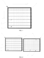
- the positions of the colloids do not overlap contact positions of the fine grid lines and the welding strips, and the consumption of adhesive for the colloids is relatively few, which can avoid the problem of electrical failure of the fine grid lines and the welding strips caused by the flow of the colloids in processes of pre-welding and fixing. As shown in FIG.
- the colloids 4 are distributed at junctions of welding strips 2 and a cell 1, and in order to avoid the problem of electrical failure of fine grid lines 3 and the welding strips 2, distribution positions of colloids 4 do not contact the fine grid lines 3, but are only configured to fix the welding strips 2, which are thus fixed on the surface of the cell 1.
- each welding strip 2 there are at least two colloids 4. That is, each welding strip is bonded to the surface of the cell by at least two colloids 4.
- the number of colloids can be determined through experiments in accordance with the dimension of the cell and the consumption of adhesive.
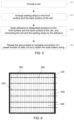
- FIG. 2 which is a schematic diagram of the connection between two adjacent cells, a plurality of first fine grid lines 31 and a plurality of first welding strips 21 perpendicular to the first fine grid lines 31 are provided on a front cell surface of a first cell 11.
- a front cell surface of a second cell 12 is provided with a plurality of second fine grid lines 32 and a plurality of second welding strips 22 perpendicular to the second fine grid lines 32.
- the first fine grid lines 31 are electrically connected to corresponding first welding strips 21, and the first welding strips 21 are fixed on the front cell surface of the first cell 11 through first colloids 41 so that the first welding strips 21 and the first cell 11 are fixed and form a mechanical connection.
- the second fine grid lines 32 are electrically connected to corresponding second welding strips 22, and the second welding strips 22 are fixed on the front cell surface of the second cell 12 through second colloids 42 so that the second welding strips 22 and the second cell 12 are fixed and form a mechanical connection.
- Positions where the first colloids 41 and the second colloids 42 are located do not overlap contact positions of corresponding welding strips and fine grid lines.
- Another part of the plurality of first welding strips 21 are arranged on a back cell surface (not shown in the drawings) of the second cell 12 in the same manner; and likewise, another part of the plurality of second welding strips 22 are arranged on a back cell surface of an adjacent cell connected in series with the second cell 12 in the same manner.
- Step S22 uniformly providing a plurality of welding strips at intervals along a direction perpendicular to the fine grid lines on the surface of each cell.
- each welding strip is perpendicular to each fine grid line on a corresponding cell surface.
- the cell to which the packaging method for a solar cell module in the first aspect is directed is a main-grid-free cell, that is, there are only the fine grid lines on the front cell surface and the back cell surface, but without the main grid line.
- both the front cell surface and the back cell surface are printed and arranged with a plurality of fine grid lines 3.
- Adjacent welding strips 2 have the predetermined spacing distance therebetween, and each welding strip 2 is perpendicular to each fine grid line 3 on the surfaces of the cell 1.
- a direction A is an extending direction of the fine grid lines 3, i.e., an arrangement direction of the welding strips 2; and a direction B is an extending direction of the welding strips 2, i.e., an arrangement direction of the fine grid lines 3.
- the cells in the present embodiment all refer to solar cells.
- a plurality of welding strips 2 perpendicular to the fine grid lines 3 are provided at intervals in sequence along the direction perpendicular to the fine grid lines 3.
- a plurality of cells need to be connected in series to be made into a cell string, and then a plurality of cell strings are typesetted, reflow-soldered, and then laminated to obtain a cell string laminate. Therefore, a plurality of cells are connected in series through the welding strips to be made into the cell string in the present embodiment. That is, by providing one or more welding strips between adjacent cells, the connection between two adjacent cells is realized, and further a plurality of cells are made into the cell string.
- each welding strip has one part arranged on a front surface of one cell, and the other part arranged on a back surface of the other cell.
- a plurality of cells can be connected in series to be made into a cell string, so as to facilitate subsequent typesetting and lamination and obtain the cell string laminate.
- Step S23 applying a preset pressure to each welding strip on each cell, so that each welding strip is bonded to a corresponding cell through corresponding colloids, and each welding strip is in direct contact with each fine grid line on the surface of the corresponding cell.
- each welding strip is in direct contact with corresponding colloids, and is bonded to the cell through the colloids. Moreover, under the effect of the pressure applied, each welding strip is also in direct contact with each fine grid line to implement the electrical connection.
- a plurality of welding strips are uniformly arranged by a wiring mechanism along the extending direction perpendicular to the fine grid lines on the surface of the cell, ensuring that any two adjacent welding strips have the same spacing distance therebetween.
- the welding strip is a copper strip with a coating.
- the coating may be a tin coated layer, a SnBiAg (silver tin bismuth) alloy layer, or other low-melting-point metal layer or alloy layer.
- a low-melting-point metal coating or alloy coating on an outer layer of the welding strip, it can be ensured in subsequent processes that the coating of the welding strip and the silver paste of the fine grid lines easily form a good alloy connection by means of heating. Due to the relatively low melting point of the coating, a heating temperature does not need to be too high, facilitating process operations.
- the low-melting-point metal layer or alloy layer has a melting point ranging from 120 °C to 160 °C.
- each solar cell module is obtained by connecting a plurality of cells in series, and two adjacent cells are connected together through the welding strips. Therefore, when wiring is performed, one welding strip has one part being wired on the front surface of one of the adjacent cells, and the other part being wired on the back surface of the other one of the adjacent cells.
- the step of printing the main grid lines is omitted in the manufacture of the cell.
- the arrangement of welding strip fixing points i.e., positions of the colloids, has a high degree of freedom.
- the mass production can be improved, and the bonding strength per unit area between the non-conductive adhesive and the welding strip can be increased and the consumption of adhesive can be reduced.
- the method further can include: pre-welding each welding strip on each cell, so that each welding strip is fixed on the surface of the corresponding cell, and each welding strip is in direct contact with the fine grid lines on the surface of corresponding cell.
- a manner of pre-welding is any one of infrared heating, heat conduction, induction heating, and heat sealing heating.
- the colloids are provided at the welding strip fixing points on the surface of the cell, when pre-welding the welding strips, the colloids can be heated, so that the welding strips are bonded to the surface of the cell through the colloids, and the mechanical connection is formed between the welding strips and the surface of the cell. Moreover, in the process of laminating the welding strips, the welding strips are brought to be a tight contact with the fine grid lines on the surface of the cell, that is, welding points and the fine grid lines are made to implement an electrical connection.
- the colloids can be selected from hot-melt adhesive, photosensitive adhesive, adhesive tape, or the like.
- the consumption of adhesive is relatively few, which can solve the problem of electrical failure of the welding strips and the fine grid lines caused by a large consumption of adhesive in the related art.
- the welding strips are bonded to the cell through the colloids, which not only can ensure that a plurality of cells are connected in series to be made into the cell string, but also can ensured that the welding strips do not move on the cell, thus preparing for a next step of packaging of the cell module.
- the colloids are provided on the surface of each cell; then the welding strips are arranged on the surface of the cell, so that the welding strips are perpendicular to the fine grid lines; finally, the welding strips are fixed on the cell through the colloids and the welding strips are brought into tight contact with the corresponding fine grid lines by means of pre-welding and/or fixing.
- pre-welding and/or fixing it not only can ensure that the welding strips will not move during the manufacturing process, and the mechanical connection between the welding strips and the cell is ensured, but also can ensure that the tight contact between the welding strips and the fine grid lines implements a stable electrical connection.
- the adhesive is applied before the wiring, it is more convenient to be operated, and conducive to be implemented for mass production in the practical production process.
- Step S3 performing typesetting and welding bus bars on the plurality of cell strings to obtain the cell string laminate.
- the plurality of cell strings can be directly typesetted, and then the bus bars are welded on the plurality of typesetted cell strings, so as to ensure that the plurality of cell strings are made into the cell module.
- Step S4 heating and laminating the cell strings, so that each welding strip forms an alloy connection with the fine grid lines on the surface of corresponding cell, so as to complete the packaging of the solar cell module.
- a temperature range of heating and laminating is from 130 °C to 170 °C.
- the coating of the welding strips is a low-melting-point metal layer or alloy layer in the present embodiment, wherein a melting point temperature is from 120 °C to 160 °C, when heating and laminating, the temperature can reach the melting point of the coating, thus, the coating on the surface of welding strip can form a good alloy connection with the silver paste of the fine grid lines.
- the coating is a tin layer or a SnBiAg alloy layer. Therefore, in the packaging method for a solar cell module in the first aspect, since it is unnecessary to print the main grid lines on the cell, and the welding strip is directly electrically connected to the fine grid lines, the consumption of silver paste is greatly reduced, and the electrical conductivity of the cell can also be improved.
- the present embodiment is more applicable to the packaging of cells with a huge amount of fine grid lines. Specifically, the present embodiment is applied to cells with the number of fine grid lines ranging from 15 to 35.
- the packaging method for a solar cell module in the first aspect does not require printing the main grid lines on the cell, thus the manufacturing cost of the cell module can be greatly reduced; compared with the manner of using the intelligent wire, as no manufacturing steps need to be added in the present embodiment, only the existing series welding process of cells is correspondingly adjusted, and no additional manufacturing equipment and manufacturing processes need to be added, thus the manufacturing costs are further saved; moreover, the welding strip in the present disclosure is a common existing welding strip, without the need of coating a polymeric film layer on the copper strip, saving the material costs, therefore, compared with the manner with the intelligent wire, it not only can greatly reduce the consumption of silver paste, but also achieve real cost reduction of the costs of the cell module.
- each welding strip is limited by a pre-crosslinked packaging film in the present embodiment.
- the welding strips can be prevented from moving on the surface of the cell, so that the problem that the welding strips are easy to move and the connection thereof is poorly implemented during lamination is solved, and good contact between each welding strip and the fine grid lines on the surface of corresponding cell can be ensured, further implementing the relatively stable mechanical connection and the alloy electrical connection.
- the pre-crosslinked packaging film in the present embodiment is a packaging adhesive film with low fluidity.
- the packaging adhesive film with low fluidity in the process of heating and laminating, the packaging adhesive film will not flow, which not only does not drive displacement of the welding strips, but also can well fix the welding strips on the surface of the cell, and press the welding strips so that the welding strips are in tight contact with the fine grid lines on the surface of the cell, thereby forming good alloy contact.
- the pre-crosslinked packaging film is made of any packing material of EVA, POE, and PVB.
- EVA refers to an ethylene-vinyl acetate copolymer and a rubber-plastic foam material made thereof.
- POE is an ethylene-octene copolymer.
- PVB refers to polyvinyl butyral.
- a solar cell module is further provided.
- the solar cell module is a solar cell module manufactured by the packaging method for a solar cell module according to the first aspect.
- the cell to which the packaging method for a solar cell module in the first aspect is directed is a main-grid-free cell, wherein the front surface and the back surface of the cell are only printed with the fine grid lines.
- the surfaces of the cells do not need to be printed with the main grid lines, and any other materials and manufacturing costs are not added, the consumption of silver paste for the cell module is significantly reduced, the manufacturing costs of the cell module is saved, and the number of cell modules is reduced.
- this packaging method does not need to add any process flow, and can be achieved by directly using existing technological devices, which is convenient for operations and saves the manufacturing costs.
- the inventors of the present disclosure found during research that, if the adhesive is first used on the cells and then the welding strips are arranged for the connection, as the height of the adhesive is not easy to control when applying the adhesive, the height of the adhesive is likely to be too high and causes a relatively large gap between the welding strips and the fine grids, which may cause poor conduction between the welding strips and the fine grid lines.
- a connection method for a solar cell string which can avoid the problem that a gap exists between the welding strips and the fine grid lines due to the adhesive is too high when the adhesive is applied, and thus can improve the problem of poor conduction between the welding strips and the fine grid lines on the cells.
- connection method for a solar cell string includes following steps: S31, providing a cell 100.
- a front surface and a back surface of the cell 100 have no main grid line or contain fine main grid lines.
- the main grid line refers to a structure having a pad on the fine main grid lines. That is to say, the front surface and the back surface of the cell 100 can be printed with fine grid lines 300, but without the main grid line, which can save the consumption of silver paste and thus can save the costs.
- both the front surface and the back surface of the cell 100 are printed with the fine grid lines 300 and the fine main grid lines, i.e., the pad on the fine main grid line is not printed, which also can save the consumption of silver paste.
- the number of fine grid lines 300 on each of the front surface and the back surface of the cell 100 ranges from 15 to 35, for example, at least one numerical value of 15, 20, 25, 30, and 35 or a range between any two values thereof.
- the fine grid lines 300 are all distributed on the front surface and the back surface of the cell 100 at a certain spacing distance.
- the cell 100 may be any one of a heterojunction cell, a TOPCON cell, and a PERC cell.
- the plurality of welding strips 200 are arranged perpendicular to the fine grid lines 300 on the cell 100.
- the plurality of welding strips 200 are arranged at a certain spacing distance from each other. It should be noted that optionally, when arranging the welding strips 200, an included angle between an welding strip 200 and an fine grid line 300 also may be an acute angle.
- the designated positions on the front surface and the back surface of the cell 100 are determined by marks screen-printed on the cell 100, wherein when screen-printing the fine grid lines 300, a plurality of marks are printed on the cell 100, and the marks can be determined as designated positions with the adhesive.
- the designated positions may be on part of the fine grid lines 300, and also may be positions between the fine grid lines 300 (see FIG. 6 ).
- the adhesive when the designated positions with the adhesive are on the fine grid lines 300, after the welding strips 200 are arranged on the front surface and the back surface of the cell 100, the adhesive is applied to positions where the welding strips 200 overlap the fine grid lines 300 to form the colloids, so that the cell 100 is connected to the welding strips 200.
- the designated positions for applying the adhesive are at positions between the fine grid lines 300, after the welding strips 200 are arranged on the front surface and the back surface of the cell 100, the adhesive is applied to positions where the welding strips 200 do not overlap the fine grid lines 300 to form the colloids, so that the cell 100 is connected to the welding strips 200.
- the adhesive used in the step of applying the adhesive is at least one of hot-melt adhesive, photosensitive adhesive, and an adhesive tape.
- the adhesive tape is used for bonding, whether the designated positions are on part of the fine grid lines 300 or between the fine grid lines 300, the adhesive tape is just directly adhered to an upper surface of each welding strip 200 and is connected to the cell 100.
- each welding strip 200 has at least two connection points with one cell 100. As there are at least two connection points, the welding strip 200 can be more stably connected to the cell 100 , and the welding strip 200 is not easy to be displaced.
- the colloids in the embodiments of the present disclosure may be conductive adhesive or non-conductive adhesive.
- the adhesive is applied to form the colloids to bond the cell 100 and the welding strips in the embodiment of the present disclosure, whether conductive adhesive or the non-conductive adhesive is used, and the positions of using the adhesive are on part of the fine grid lines 300 or between the fine grid lines 300, after the cell 100 is bonded to the welding strips 200, it can be relatively easy for the welding strips 200 and the fine grid lines 300 on the cell 100 to contact, so that the welding strips 200 and the fine grid lines 300 enable a good electrical contact.
- step S32 and before step S33 further included is: a step of enabling a preliminary connection between the welding strips 200 and the fine grid lines 300 of the cell 100 by heating.
- the welding strips 200 are arranged on the surface of the cell 100, then the preliminary connection between the welding strips 200 and the fine grid lines 300 is implemented by means of heating, then the colloids 400 are formed at designated positions on the front surface and the back surface of the cell 100, and the cell 100 is connected to the welding strips 200 through the colloids 400, which can further improve the connection stability of the welding strips 200 and the cell 100, and can further improve the electrical contact between the welding strips 200 and the fine grid lines 300, thus, the problem of poor conduction between the welding strips 200 and the cell 100 is further solved.
- the preliminary connection formed by the welding strips 200 and the fine grid lines 300 on the cell 100 may be preliminary contact of the welding strips 200 and the fine grid lines 300, and also may be a relatively weak alloy connection formed by welding strips 200 and the fine grid lines 300, in this case the welding strips 200 may be separated from the fine grid lines 300 by a relatively less force. Subsequently, the welding strips 200 and the grid lines 300 can form tight contact or a relatively strong alloy connection after being laminated and heated, and a greater force is required to separate the welding strips 200 from the fine grid lines 300.
- both the preliminary contact and the tight contact refer to a state in which the welding strips 200 and the fine grid lines 300 on the cell 100 are in mechanical contact, while the alloy connection is not formed.
- a separating force after the preliminary connection between the welding strips 200 and the fine grid line 300 is formed ranges from 0.03N to 0.1 N, which can ensure that the welding strips 200 do not move on the cell 100 without an external force, and makes the contact of the welding strips 200 and the fine grid lines 300 more tight.
- the separating force refers to a force required for separating the welding strips 200 and the fine grid lines 300 after the preliminary connection between the welding strips 200 and the fine grid lines 300 is formed.
- the separating force after the preliminary connection between the welding strips 200 and the fine grid lines 300 is formed is any one of 0.03 N, 0.04 N, 0.05 N, 0.06 N, 0.06 N, 0.07 N, 0.08 N, 0.09 N, and 0.1 N or a range between any two thereof.
- heating manners include at least one of infrared heating, thermal conduction, induction heating, and hot air heating.
- a heating temperature of forming the preliminary connection between the welding strips 200 and the fine grid lines 300 ranges from 100°C to 250 °C, for example, any one of 100 °C, 120 °C, 140 °C, 150 °C, 170 °C, 180 °C, 200 °C, 220 °C, 240 °C, and 250 °C or a range between any two thereof.
- each welding strip 200 is a copper welding strip 200 having a coating on an entire surface, wherein the coating includes a metal layer or an alloy layer with a melting temperature ranging from 120 to 160 °C.
- the metal layer or the alloy layer has a relatively low melting temperature, a good connection between the welding strips 200 and the fine grid lines 300 can be achieved through a relatively low heating temperature.
- a good connection between the welding strips 200 and the fine grid lines 300 also can be realized through a relatively low temperature, thus the process operations can be facilitated.
- the melting temperature of the metal layer or the alloy layer is any one of 120 °C, 130 °C, 140 °C, 150 °C, and 160 °C or a range between any two thereof.
- the coating is a Sn alloy layer, and the Sn alloy layer has a relatively low melting temperature, then a good connection between the welding strips 200 and the fine grid lines 300 can be achieved through a relatively low laminating and heating temperature.
- the Sn alloy layer is a SnBiAg alloy layer.
- each welding strip 200 has a thickness ranging from 0.1mm to 0.3 mm, for example, any one of 0.1 mm, 0.2 mm, and 0.3 mm or a range between any two thereof.
- the welding strips 200 may be segmented welding strips, that is to say, one welding strip 200 may have more than one cross-section shape, for example, a cross section of a part of connection between the welding strip 200 and the front surface of the cell 100 is of one shape, and a cross section of a part of connection between the welding strip 200 and the back surface of the cell 100 is of another shape.
- the cross sections of the welding strip 200 may be at least one of a circle and a triangle, and a surface of the welding strip 200 in contact with the cell 100 also may be a flat surface.
- step S33 and before step S34 further included is: a step of curing the colloids 400.
- the colloids 400 are cured after the welding strips 200 are connected to the cell 100 through the colloids 400, then the connection stability between the welding strips 200 and the cell 100 can be improved, so that the welding strips 200 are less likely to be displaced, which is more beneficial to improve the good electrical contact between the welding strips 200 and the fine grid lines 300.
- the manner of curing the colloids 400 includes heating, providing lighting or hot-pressing.
- heat-sensitive adhesive is selected as the colloids 400
- the colloids 400 can be cured by heating
- the photosensitive adhesive when the photosensitive adhesive is selected as the colloids 400, the photosensitive adhesive can be cured by providing lighting; and when heat-pressure-sensitive adhesive is used, the colloids 112 can be cured by means of hot-pressing.
- connection method for a solar cell string is provided, specifically illustrated as follows.
- FIG. 7 shows a flowchart of a connection method for a solar cell string in the fourth aspect, wherein the cell string includes a plurality of cells connected in series, two adjacent cells are connected together through welding strips, the welding strips are segmented welding strips, each including a first segment and a second segment, and specific steps of the connection method include: S41, arranging a first welding strip 210, and applying adhesive to an upper surface of the first segment of the first welding strip 210 to form colloids 400 (see FIG. 8 ).
- first welding strip 210 when arranging the first welding strip 210, a plurality of welding strips are arranged, wherein the plurality of first welding strips 210 are arranged at intervals of a certain spacing distance.
- the plurality of first welding strips 210 are arranged in parallel.
- the adhesive 400 Since the adhesive is applied to the upper surface of the first segment of the first welding strip 210, and then the cell 100 is arranged on the upper surface of the first segment of the first welding strip 210 for bonding, the adhesive 400 will not easily drip on the upper surface of the first welding strip 210, so that the problem of poor bonding effect between the welding strip and the cell 100 caused by the adhesive dripping can be avoided.
- the upper surface of the first segment of each first welding strip 210 is a flat surface.
- the upper surface of the first segment of the first welding strip 210 is provided as a flat surface, so that it is easy to apply the adhesive to the upper surface of the first segment, and the adhesive will not easily drip from the upper surface, thus facilitating the subsequent stable connection between the first segment 220 of the first welding strip 210 and the cell 100.
- the upper surface of the first segment of the first welding strip 210 has a width ranging from 0.2 to 1.2 mm.
- the upper surface within this width range is beneficial to more stably dispense the adhesive on the welding strip and the adhesive is not easy to drip.
- the width of the upper surface is any one of 0.5 mm, 0.6 mm, 0.7 mm, 0.8 mm, 0.9 mm, 1.0 mm, 1.1 mm, and 1.2 mm or a range between any two thereof.
- the lower surface of the first segment may be a flat surface, a cambered surface, or of other shapes, which is not specifically limited in the embodiments of the present disclosure.
- a cross section of the second segment of a second welding strip 220 includes at least one of a circle and a triangle.
- a front surface and the back surface of the cell 100 have no main grid line or contain fine main grid lines. That is to say, the grid lines on the front surface and the back surface of the cell 100 only contain fine grid lines, or contain fine grid lines and fine main grid lines without the bonding pad.
- the cell 100 also may be a cell 100 containing the main grid lines.
- the fine grid lines on the cell 100 are arranged in a perpendicular relationship with the first welding strip 210.
- the number of fine grid lines on the front surface of the cell 100 ranges from 15 to 35, and the number of fine grid lines on the back surface of the cell 100 is also 15 to 35.
- the fine grids on the front surface of the cell 100 are distributed on the surface of the cell 100 at certain intervals, and the fine grid lines on the back surface of the cell 100 are also distributed on the surface of the cell 100 at certain intervals.
- the cell 100 is any one of heterojunction cell, TOPCON cell, and PERC cell.
- the preset positions on the front surface of the cell 100 are determined by marks screen-printed on the cell 100.
- a plurality of marks are printed on the cell 100, and the marks can be determined as preset positions for applying the adhesive.
- the preset positions are on part of the fine grid lines. It can be understood that the preset positions also may be positions between two adjacent fine grid lines, rather than on the fine grid lines.
- the second welding strip 220 As the adhesive is applied to the preset positions on the front surface of the cell 100, then the second welding strip 220 is placed on the front surface of the cell 100 for bonding, the adhesive dispensed on the front surface of the cell 100 is not easy to drip, therefore, the problem of poor bonding effect between the cell 100 and the welding strip caused by the adhesive dripping can be avoided.
- a plurality of welding strips are arranged, wherein the plurality of second welding strips 220 are arranged at intervals of a certain spacing distance.
- the plurality of second welding strips 220 are arranged in parallel.
- the plurality of second welding strips 220 are arranged in a perpendicular relationship with the fine grid lines on the cell 100.
- the adhesive continues to be applied to the upper surfaces of the first segments of the second welding strips 220, then another cell 100 is arranged on the upper surfaces of the first segments of the second welding strips 220, after a back surface of the another cell 100 is connected to the first segments of the second welding strips 220, steps that need to be repeated are performed in sequence, and finally, a plurality of cells 100 are connected in series to be made into the cell string.
- the colloids used are conductive adhesive or non-conductive adhesive. In either case of using the conductive adhesive or the non-conductive adhesive, good electrical contact can be formed between the cells and the welding strips.
- the colloids used are non-conductive adhesive, and the preset positions are not on the fine grid lines.
- the non-conductive adhesive is used, and the positions for applying the adhesive are not on the fine grid lines, for example, are between two fine grid lines, when connecting the welding strips and the cells 100, it is beneficial for the contact between the welding strips and the fine grid lines, thus better electrical contact can be formed between the welding strips and the fine grid lines on the cells 100.
- the colloids used include at least one of hot-melt adhesive and photosensitive adhesive.
- a step of curing the adhesive is further included.
- the connection between the welding strips and the cell 100 can be reinforced, thus improving the connection stability.
- the step of curing the adhesive is performed by means of heating, lighting or hot-pressing.
- a temperature for curing the adhesive ranging from 100 °C to 250 °C, for example, any one of 100 °C, 120 °C, 150 °C, 180 °C, 200 °C, and 250 °C or a range between any two thereof.
- heating manners for curing the adhesive include at least one of infrared heating, thermal conduction, induction heating, and hot air heating.
- connection method for a solar cell string in the fourth aspect is described by taking connecting two cells as an example, which includes steps of: a) arranging the first welding strip, and applying the adhesive to the upper surface of the first segment of the first welding strip; b) arranging the first cell on the first segment of the first welding strip, so that the back surface of the first cell is connected to the first segment of the first welding strip; c) applying the adhesive to the preset positions on the front surface of the first cell; d) arranging the second segment of the second welding strip to the front surface of the first cell, so that the second segment of the second welding strip is connected to the front surface of the first cell; e) applying the adhesive to the upper surface of the first segment of the second welding strip; f) arranging the second cell on the first segment of the second welding strip, so that the back surface of the second cell is connected to the first segment of the second welding strip; g) applying the adhesive to the presets positions on the front surface of the second cell; and h) arranging a second segment of
- connection method for a solar cell string in the fourth aspect is described by taking connecting three cells as an example, which includes steps of: the above steps a) ⁇ h) (description is omitted herein); i) applying the adhesive to an upper surface of a first segment of the third welding strip; j) arranging a third cell on the first segment of the third welding strip, so that a back surface of the third cell is connected to the first segment of the third welding strip; k) applying the adhesive to preset positions on a front surface of the third cell; and I) arranging a second segment of a fourth welding strip on the front surface of the third cell, so that the second segment of the fourth welding strip is connected to the front surface of the third cell, thus obtaining the cell string.
- the adhesive is applied to the upper surface of the first welding strip, then the cell is arranged on the upper surface of the first segment of the first welding strip for bonding, after that, the adhesive is applied to the preset positions on the front surface of the cell, and the second welding strip is arranged on the front surface of the cell for bonding.
- the adhesive is applied to the upper surface of the welding strip and the front surface of the cell, the problem of poor bonding effect between the cell and the welding strips caused by adhesive dripping can be avoided.
- a further connection method for a solar cell string is provided.
- FIG. 12 shows a flowchart of the connection method for a solar cell string in the fifth aspect, wherein the cell string includes a plurality of cells 100 connected in series, two adjacent cells 100 are connected together through welding strips, the welding strips are segmented welding strips, each including a first segment and a second segment, and the connection method includes: S51: providing a cell 100, and applying adhesive to designated positions on a back surface of the cell 100 to form colloids 400 (see FIG. 13 ).
- a front surface and the back surface of the cell 100 both have no main grid line or contain fine main grid lines.
- the grid lines on the front surface and the back surface of the cell 100 may be only fine grid lines, and also may be fine grid lines and fine main grid lines.
- the number of fine grid lines on the front surface and the back surface of the cell 100 ranging from 15 to 35, while the number of fine grid lines is not limited thereto, and may be appropriately increased or reduced according to the design of the cell, for example, the number may be up to 100, that is, the number of fine grid lines may be any integer ranging from 1 to 100.
- the fine grid lines are distributed on the front surface and the back surface of the cell 100 at a certain spacing distance.
- the cell 100 is any one of heterojunction cell, TOPCON cell, and PERC cell.
- the designated positions on the cell 100 are determined by marks screen-printed on the cell 100.
- the preset positions may be on part of the fine grid lines, and also may be not on the fine grid lines, but at positions between two adjacent fine grid lines.
- the arranged first welding strip 210 may be arranged before applying the adhesive to the designated positions on the back surface of the cell 100, and also may be arranged after applying the adhesive to the designated positions on the back surface of the cell 100 to form the colloids 400.
- a plurality of first welding strips 210 can be arranged, wherein the plurality of first welding strips 210 are arranged at a certain spacing distance.
- the fine grid lines on the cell 100 can be made to maintain a perpendicular relationship with the first welding strip 210.
- S54 arranging the second segment of a second welding strip 220 on the front surface of the cell 100, so as to make the second segment of the second welding strip 220 connected with the front surface of the cell 100 (see FIG. 16 ).
- a plurality of second welding strips 220 can be arranged, wherein the plurality of second welding strips 220 are arranged on the front surface of the cell 100 at a certain spacing distance.
- the second welding strips 220 when arranging the second welding strips 220, they can be arranged along a direction perpendicular to the fine grid lines on the front surface of the cell 100.
- the adhesive is applied to designated positions on a back surface of another cell 100, then the another cell 100 is arranged on the first segments of the second welding strips 220, and the back surface of the another cell 100 is connected to the first segments of the second welding strips 220; the adhesive continues to be applied to designated positions on the front surface of the another cell 100, then steps that need to be repeated are performed in sequence, and finally, a plurality of cells 100 are connected to be made into the cell string.
- connection method for a solar cell string in the fifth aspect first, the adhesive is applied to the designated positions on the back surface of the cell 100, then the back surface of the cell is connected to the welding strips, and the adhesive is applied to the designated positions on the front surface of the cell 100, after that the welding strips are connected to the front surface of the cell.
- first the adhesive is applied to one surface of the cell 100, and the surface of the cell 100 to which the adhesive is applied is connected to the welding strips and then can be placed on a bearing platform, after that the adhesive is applied to the other surface of the cell. In this way, the operations are convenient, and the problem that it is inconvenient to apply the adhesive to the front and back surfaces of the cell 100 is solved.
- the adhesive used in the step of applying the adhesive is conductive adhesive.
- the conductive adhesive itself has a conductive function and can lead out current of the cell 100.
- the adhesive used in the step of applying the adhesive also may be non-conductive adhesive.
- the designated positions are not on the fine grid lines but between two adjacent fine grid lines. With such configuration, after the welding strips are connected to the cell 100, it is easier for the welding strips to contact the fine grid lines on the cell 100, thus, the welding strips and the fine grid lines on the cell 100 can enable good electrical contact.
- the designated positions are in a central line region between two adjacent fine grid lines. It should be noted that, two adjacent fine grid lines are arranged in parallel, so that the central line and the fine grid lines are also arranged in parallel, and a middle point of a perpendicular line connecting two adjacent fine grid lines is located on the central line.
- the central line region refers to a region that is widened by a preset distance in a direction close to two fine grid lines based on the central line, and optionally, the preset distance ranges from 1/6 to 2/3 of a distance between two adjacent fine grid lines. In the above, the preset distance also refers to a width of a central line region. If the designated positions are located in the central line region between two adjacent fine grid lines, when bonding the welding strips and the colloids 400, the colloids 400 will not easy to overflow onto the fine grid lines to affect the electrical contact between the welding strips and the fine grid lines.
- the adhesive used in the step of applying the adhesive includes at least one of hot-melt adhesive and photosensitive adhesive.
- a step of curing the colloids 400 is further included between step S54 and step S55.
- the connection stability between the welding strips and the cell 100 can be increased.
- the manner of curing the colloids 400 includes heating, lighting or hot-pressing, for example, when the hot-melt adhesive is used as the colloids 400, the hot-melt adhesive can be cured by heating or hot-pressing; and when the photosensitive adhesive is used as the colloids 400, the photosensitive adhesive can be cured by providing lighting.
- heating manners include at least one of infrared heating, thermal conduction, induction heating, and hot air heating.
- a heating temperature ranges from 100°C to 250 °C, for example, any one of 100 °C, 120 °C, 150 °C, 180 °C, 200 °C, 220 °C, and 250 °C or a range between any two thereof.
- connection method for a solar cell string in the fifth aspect is described by taking two cells 100 as an example, which includes steps of: aa) arranging a first welding strip 210; bb) providing a first cell, and applying adhesive to designated positions on a back surface of the first cell; cc) arranging the first cell on a first segment of the first welding strip 210, so that the back surface of the first cell is connected to the first segment of the first welding strip 210; dd) applying adhesive to designated positions on a front surface of the first cell; ee) arranging a second segment of a second welding strip 220 on the front surface of the first cell, so that the second segment of the second welding strip 220 is connected to the front surface of the first cell; ff) providing a second cell, and applying adhesive to designated positions on a back surface of the second cell; and gg) arranging the second cell on a first segment of the second welding strip 220, so that the back surface of the second cell is connected to the first segment of the second welding strip 220, thus
- connection method for a solar cell string in the fifth aspect is described by taking three cells 100 as an example, which includes the following steps: step aa) ⁇ gg) (the description is omitted herein); hh) applying adhesive to designated positions on a front surface of the second cell; and ii) arranging a second segment of a third welding strip on the front surface of the second cell, so that the second segment of the third welding strip is connected to the front surface of the second cell, thus obtaining the cell string.
- connection method for a solar cell string in the fifth aspect first, the adhesive is applied to the designated positions on the back surface of the cell, then the back surface of the cell is connected to the welding strips, and the adhesive is applied to the designated positions on the front surface of the cell, after that the welding strips are connected to the front surface of the cell.
- first the adhesive is applied to one surface of the cell, and the surface of the cell to which the adhesive is applied is connected to the welding strips and then can be placed on a bearing platform, after that the adhesive is applied to the other surface of the cell, in this way, the operations can be facilitated.
- a manufacturing method for a solar cell module including the connection method for a solar cell string in the third aspect, the fourth aspect or the fifth aspect, and heating and laminating the obtained cell strings.
- the electrical contact and the connection stability between the fine grid lines and the welding strips of the cells can be further improved, which facilitates leading out the current of the cell strings, and thus improves the structural stability of the solar cell module.
- the welding strips form tight contact or alloy connection with the fine grid lines on the cells.
- the connection between the cells and the welding strips is more stable, and the welding strips form good electrical contact with the cells.
- the tight contact refers to that the fine grid lines on the cells are in contact with the welding strips, and the fine grid lines are in tight contact with the welding strips through the laminating process, but the surfaces of the welding strips and the metal of the fine grid lines are not melted to form an alloy.
- each welding strip includes a copper substrate and a film layer on a surface of the copper substrate, and the film layer includes a metal layer or an alloy layer with a melting temperature of 120 to 160 °C.
- the film layer on the surface of the welding strip in the embodiments of the present disclosure contains a metal layer or an alloy layer with a melting temperature ranging from 120°C to 160 °C, therefore, the metal layer or the alloy layer can be melted by a relatively low temperature, and form a good alloy connection with the cells in the processes of laminating and heating. As a relatively low temperature is easier to reach in the operations, it is more convenient for process operations.
- the film layer is a Sn alloy layer, for example, Sn alloy in the Sn alloy layer includes SnBiAg.
- the melting temperature of the metal layer or the alloy layer is any one of 120 °C, 130 °C, 140 °C, 150 °C, and 160 °C or a range between any two thereof.
- a temperature of heating and laminating ranges from 130 °C to 170 °C. The lower the temperature of heating and laminating is, the easier it is to achieve during the process operations.
- the temperature of heating and laminating is any one of 130 °C, 140 °C, 150 °C, 160 °C, and 170 °C or a range between any two thereof.
- steps such as performing typesetting, welding bus bars, and EL test on the cell strings are further included.
- the manufacturing method for a solar cell module in the sixth aspect includes performing typesetting, welding bus bars, and then heating and laminating on the cell strings obtained by the connection method for a solar cell string in the third aspect, the fourth aspect or the fifth aspect,
- a solar cell module is provided, which is manufactured by the above manufacturing method for a solar cell module.
- the colloids are formed by applying the adhesive, wherein the meaning of applying the adhesive includes actions of performing dispensing, spraying, printing etc. on the adhesive to form the colloids.
- the present disclosure is applied to the packaging method for a solar cell module, the connection method for a solar cell string, and the solar cell module and the preparation method therefor. Since the cells do not need to be printed with the main grid lines, the welding strips are directly fixed on the cells and the electrical connection between the welding strips and the fine grid lines is ensured, so that not only the conductive function of the solar cell module is achieved, but also the consumption of silver paste can be greatly reduced, further reducing the costs of the cell module.
Landscapes
- Photovoltaic Devices (AREA)
Applications Claiming Priority (5)
| Application Number | Priority Date | Filing Date | Title |
|---|---|---|---|
| CN202011613801.7A CN114765229A (zh) | 2020-12-30 | 2020-12-30 | 一种太阳能电池组件的封装方法及太阳能电池组件 |
| CN202111294050.1A CN114023840A (zh) | 2021-11-03 | 2021-11-03 | 太阳能电池串的连接方法、太阳能电池组件的制作方法 |
| CN202111295283.3A CN114023842B (zh) | 2021-11-03 | 2021-11-03 | 太阳能电池串的连接方法、太阳能电池组件及其制备方法 |
| CN202111295282.9A CN114023841A (zh) | 2021-11-03 | 2021-11-03 | 太阳能电池串的连接方法、太阳能电池组件及其制备工艺 |
| PCT/CN2021/137197 WO2022143109A1 (zh) | 2020-12-30 | 2021-12-10 | 太阳能电池组件的封装方法、太阳能电池串的连接方法、太阳能电池组件及其制备方法 |
Publications (2)
| Publication Number | Publication Date |
|---|---|
| EP4228010A1 true EP4228010A1 (de) | 2023-08-16 |
| EP4228010A4 EP4228010A4 (de) | 2024-05-29 |
Family
ID=82259036
Family Applications (1)
| Application Number | Title | Priority Date | Filing Date |
|---|---|---|---|
| EP21913850.0A Pending EP4228010A4 (de) | 2020-12-30 | 2021-12-10 | Verpackungsverfahren für ein solarzellenmodul, verbindungsverfahren für einen solarzellenstrang, solarzellenmodul und herstellungsverfahren dafür |
Country Status (4)
| Country | Link |
|---|---|
| US (1) | US20240194820A1 (de) |
| EP (1) | EP4228010A4 (de) |
| AU (1) | AU2021411631B2 (de) |
| WO (1) | WO2022143109A1 (de) |
Cited By (1)
| Publication number | Priority date | Publication date | Assignee | Title |
|---|---|---|---|---|
| CN117637890A (zh) * | 2023-11-28 | 2024-03-01 | 江苏海博瑞光伏科技有限公司 | 一种无主栅组件及其制备方法 |
Families Citing this family (14)
| Publication number | Priority date | Publication date | Assignee | Title |
|---|---|---|---|---|
| CN115172524B (zh) * | 2022-07-13 | 2024-08-20 | 通威太阳能(合肥)有限公司 | 一种太阳电池及其互联方法 |
| CN115241294B (zh) * | 2022-07-21 | 2024-05-17 | 常州时创能源股份有限公司 | 一种光伏叠瓦组件及其制备方法 |
| DE102022122448A1 (de) * | 2022-09-05 | 2024-03-07 | Hanwha Q Cells Gmbh | Solarmodul-Halbzeug und Verfahren zur Herstellung eines Solarmoduls |
| CN115295656A (zh) * | 2022-10-08 | 2022-11-04 | 浙江制能科技有限公司 | 一种电池组件制作方法 |
| CN115663035A (zh) * | 2022-11-11 | 2023-01-31 | 浙江制能科技有限公司 | 一种无主栅组件及制作方法 |
| CN116093170A (zh) * | 2022-10-24 | 2023-05-09 | 天合光能股份有限公司 | 施胶互连防断路的栅线结构及太阳能电池和施胶方法 |
| CN116093167B (zh) * | 2022-12-19 | 2024-10-15 | 无锡荷雨新能源科技有限公司 | 一种电池组件、光伏组件及其制备方法 |
| CN219642849U (zh) * | 2022-12-30 | 2023-09-05 | 中能创光电科技(常州)有限公司 | 光伏电池串及光伏组件 |
| CN116154011B (zh) * | 2023-04-19 | 2023-06-23 | 金阳(泉州)新能源科技有限公司 | 一种可卷绕的轻质光伏组件 |
| CN116207188B (zh) * | 2023-04-28 | 2023-07-07 | 苏州智慧谷激光智能装备有限公司 | 无主栅式电池片串接方法以及相应的串接设备 |
| CN117976751B (zh) * | 2024-04-01 | 2024-06-28 | 苏州智慧谷激光智能装备有限公司 | 电池串、电池串制备方法以及电池串制备装置 |
| CN119029086A (zh) * | 2024-08-16 | 2024-11-26 | 中国长江三峡集团有限公司 | 一种太阳能电池组件的封装方法与系统 |
| CN118919594B (zh) * | 2024-09-29 | 2025-02-07 | 浙江爱旭太阳能科技有限公司 | 一种太阳电池组件和光伏系统 |
| CN119604084B (zh) * | 2024-12-10 | 2025-10-17 | 江门普乐开瑞太阳能科技有限公司 | 无主栅背接触太阳能电池片、背接触太阳能电池串和光伏组件 |
Family Cites Families (28)
| Publication number | Priority date | Publication date | Assignee | Title |
|---|---|---|---|---|
| US4578302A (en) * | 1985-06-27 | 1986-03-25 | National Starch And Chemical Corporation | Reinforced tape laminates |
| US5021099A (en) * | 1988-08-09 | 1991-06-04 | The Boeing Company | Solar cell interconnection and packaging using tape carrier |
| DE10239845C1 (de) | 2002-08-29 | 2003-12-24 | Day4 Energy Inc | Elektrode für fotovoltaische Zellen, fotovoltaische Zelle und fotovoltaischer Modul |
| US20110239450A1 (en) * | 2008-08-11 | 2011-10-06 | Basol Bulent M | Roll-to-roll manufacturing of flexible thin film photovoltaic modules |
| CN102646728B (zh) * | 2012-05-02 | 2015-11-11 | 苏州阿特斯阳光电力科技有限公司 | 一种背接触硅太阳能电池片的背面电极结构及其制备方法 |
| CN102751360A (zh) * | 2012-07-20 | 2012-10-24 | 合肥海润光伏科技有限公司 | 光伏组件及其制作方法 |
| US20180083152A1 (en) * | 2015-06-17 | 2018-03-22 | Kaneka Corporation | Crystalline silicon solar cell module and manufacturing method for same |
| CN105762202B (zh) | 2016-04-28 | 2017-08-15 | 泰州乐叶光伏科技有限公司 | 一种点线结合的太阳能电池正面电极及其制备方法 |
| US20190341515A1 (en) * | 2016-12-08 | 2019-11-07 | Kaneka Corporation | Solar cell module |
| CN110326120B (zh) * | 2017-01-02 | 2022-11-11 | Sabic环球技术有限责任公司 | 光伏封装体和用于制造这种光伏封装体的方法 |
| CN106847968A (zh) * | 2017-02-17 | 2017-06-13 | 华东理工大学 | 一种双面晶体硅异质结无主栅太阳能电池片的封装方法 |
| EP3392916A1 (de) * | 2017-04-19 | 2018-10-24 | Heraeus Deutschland GmbH & Co. KG | Alterungsresistente aluminiumverbinder für solarzellen |
| CN207149569U (zh) * | 2017-09-27 | 2018-03-27 | 君泰创新(北京)科技有限公司 | 一种光伏组件 |
| CN107958943A (zh) * | 2017-12-26 | 2018-04-24 | 南京日托光伏科技股份有限公司 | 一种基于ibc电池封装的光伏组件及制作方法 |
| US20210082634A1 (en) * | 2018-02-14 | 2021-03-18 | Lg Electronics Inc. | Solar cell module comprising perovskite solar cell and manufacturing method thereof |
| KR102521021B1 (ko) * | 2018-03-08 | 2023-04-12 | 상라오 징코 솔라 테크놀러지 디벨롭먼트 컴퍼니, 리미티드 | 태양 전지 패널용 플럭스 도포 부재 및 방법, 그리고 태양 전지 패널의 인터커넥터 부착 장치 |
| EP3544062A1 (de) * | 2018-03-22 | 2019-09-25 | LG Electronics Inc. | Verbindungselement für solarzellenpaneel und solarzellenpaneel damit |
| US20190379321A1 (en) * | 2018-06-12 | 2019-12-12 | Tesla, Inc. | Solar roof tile connectors |
| KR102577910B1 (ko) * | 2018-09-18 | 2023-09-14 | 상라오 징코 솔라 테크놀러지 디벨롭먼트 컴퍼니, 리미티드 | 태양 전지 및 이를 포함하는 태양 전지 패널 |
| KR102624328B1 (ko) * | 2018-10-31 | 2024-01-15 | 상라오 신위안 웨동 테크놀러지 디벨롭먼트 컴퍼니, 리미티드 | 태양 전지 모듈 |
| KR102652350B1 (ko) * | 2018-11-07 | 2024-03-29 | 상라오 신위안 웨동 테크놀러지 디벨롭먼트 컴퍼니, 리미티드 | 태양 전지 모듈 |
| CN110993733A (zh) * | 2019-12-04 | 2020-04-10 | 通威太阳能(合肥)有限公司 | 一种光伏组件制作方法 |
| CN211062732U (zh) * | 2020-01-20 | 2020-07-21 | 厦门昊亮能源科技有限公司 | 一种太阳能电池板排版机 |
| CN111244216B (zh) * | 2020-01-23 | 2025-11-18 | 通威太阳能(合肥)有限公司 | 叠瓦组件的制造方法及叠瓦组件 |
| EP4139967A4 (de) * | 2020-04-21 | 2024-05-01 | SolarCA LLC | Schindelzellendesign mit reduzierter überlappung für schindelförmige tafeln |
| CN111785804A (zh) * | 2020-05-27 | 2020-10-16 | 泰州隆基乐叶光伏科技有限公司 | 一种背接触电池组件生产方法及系统 |
| KR102947921B1 (ko) * | 2021-09-10 | 2026-04-06 | 상라오 신위안 웨동 테크놀러지 디벨롭먼트 컴퍼니, 리미티드 | 태양 전지, 그의 제조 방법 및 그를 포함하는 태양 전지 모듈 |
| CN114388637B (zh) * | 2022-03-23 | 2022-06-21 | 中国华能集团清洁能源技术研究院有限公司 | 光伏电池片及其制作方法和叠瓦组件 |
-
2021
- 2021-12-10 EP EP21913850.0A patent/EP4228010A4/de active Pending
- 2021-12-10 WO PCT/CN2021/137197 patent/WO2022143109A1/zh not_active Ceased
- 2021-12-10 AU AU2021411631A patent/AU2021411631B2/en active Active
- 2021-12-10 US US18/254,314 patent/US20240194820A1/en active Pending
Cited By (1)
| Publication number | Priority date | Publication date | Assignee | Title |
|---|---|---|---|---|
| CN117637890A (zh) * | 2023-11-28 | 2024-03-01 | 江苏海博瑞光伏科技有限公司 | 一种无主栅组件及其制备方法 |
Also Published As
| Publication number | Publication date |
|---|---|
| AU2021411631A9 (en) | 2024-06-06 |
| US20240194820A1 (en) | 2024-06-13 |
| AU2021411631A1 (en) | 2023-06-15 |
| WO2022143109A1 (zh) | 2022-07-07 |
| EP4228010A4 (de) | 2024-05-29 |
| AU2021411631B2 (en) | 2024-08-08 |
Similar Documents
| Publication | Publication Date | Title |
|---|---|---|
| EP4228010A1 (de) | Verpackungsverfahren für ein solarzellenmodul, verbindungsverfahren für einen solarzellenstrang, solarzellenmodul und herstellungsverfahren dafür | |
| CN113851550B (zh) | 一种太阳能电池串及其制备方法和应用 | |
| CN106206765B (zh) | 太阳能电池片阵列、太阳能电池组件及其制备方法 | |
| CN114765229A (zh) | 一种太阳能电池组件的封装方法及太阳能电池组件 | |
| CN107195719B (zh) | 叠瓦式太阳能光伏组件的生产设备 | |
| JP3164183B2 (ja) | 光起電力素子及びモジュール | |
| CN113193058A (zh) | 一种背接触太阳能电池串及制备方法、组件及系统 | |
| EP3200240A1 (de) | Hocheffizientes rückseitenkontaktiertes solarzellenmodul ohne main-gate, anordnung und herstellungsverfahren | |
| CN207818590U (zh) | 一种双面发电太阳能电池和光伏组件 | |
| CN207624723U (zh) | 带有柔性导电条带的叠瓦式太阳能光伏组件 | |
| JP3220955U (ja) | 太陽電池ユニット及びその製造方法、アセンブリ、システム | |
| CN103646981B (zh) | 用于背接触太阳能电池组件的压花焊带及组件的制备方法 | |
| CN104160514A (zh) | 使用导电胶作为电极的硅太阳能电池模块及其制造方法 | |
| CN109904283A (zh) | 一种太阳能电池的互联制造法及其制造的太阳能电池组件 | |
| CN114023841A (zh) | 太阳能电池串的连接方法、太阳能电池组件及其制备工艺 | |
| CN104716213B (zh) | 光伏电池模块及其制作方法 | |
| US20240363781A1 (en) | Flexible photovoltaic cell module and manufacturing method thereof | |
| CN116247129A (zh) | 一种无主栅xbc电池组件的制备方法及其电池组件 | |
| JP2017533597A (ja) | 太陽電池アレイ、太陽電池モジュール、及びこれらの製造方法 | |
| JP2015185731A (ja) | 太陽電池モジュール及びその製造方法 | |
| CN214898458U (zh) | 一种背接触太阳能电池串、组件及系统 | |
| JP2014017398A (ja) | 太陽電池モジュール及びその製造方法 | |
| CN104319301A (zh) | 无主栅、高效率背接触太阳能电池背板、组件及制备工艺 | |
| CN108172654A (zh) | 太阳能电池池片组件及其组装方法 | |
| CN204905263U (zh) | 太阳能电池片阵列、太阳能电池组件 |
Legal Events
| Date | Code | Title | Description |
|---|---|---|---|
| STAA | Information on the status of an ep patent application or granted ep patent |
Free format text: STATUS: THE INTERNATIONAL PUBLICATION HAS BEEN MADE |
|
| PUAI | Public reference made under article 153(3) epc to a published international application that has entered the european phase |
Free format text: ORIGINAL CODE: 0009012 |
|
| STAA | Information on the status of an ep patent application or granted ep patent |
Free format text: STATUS: REQUEST FOR EXAMINATION WAS MADE |
|
| 17P | Request for examination filed |
Effective date: 20230512 |
|
| AK | Designated contracting states |
Kind code of ref document: A1 Designated state(s): AL AT BE BG CH CY CZ DE DK EE ES FI FR GB GR HR HU IE IS IT LI LT LU LV MC MK MT NL NO PL PT RO RS SE SI SK SM TR |
|
| DAV | Request for validation of the european patent (deleted) | ||
| DAX | Request for extension of the european patent (deleted) | ||
| STAA | Information on the status of an ep patent application or granted ep patent |
Free format text: STATUS: EXAMINATION IS IN PROGRESS |
|
| A4 | Supplementary search report drawn up and despatched |
Effective date: 20240429 |
|
| RIC1 | Information provided on ipc code assigned before grant |
Ipc: H01L 31/18 20060101ALI20240423BHEP Ipc: H01L 31/05 20140101AFI20240423BHEP |
|
| 17Q | First examination report despatched |
Effective date: 20240513 |