EP4226416B1 - Verfahren zur herstellung eines substrats für das epitaktische wachstum einer schicht aus einer galliumbasierten iii-n-legierung - Google Patents
Verfahren zur herstellung eines substrats für das epitaktische wachstum einer schicht aus einer galliumbasierten iii-n-legierung Download PDFInfo
- Publication number
- EP4226416B1 EP4226416B1 EP21801584.0A EP21801584A EP4226416B1 EP 4226416 B1 EP4226416 B1 EP 4226416B1 EP 21801584 A EP21801584 A EP 21801584A EP 4226416 B1 EP4226416 B1 EP 4226416B1
- Authority
- EP
- European Patent Office
- Prior art keywords
- layer
- substrate
- sic
- semi
- process according
- Prior art date
- Legal status (The legal status is an assumption and is not a legal conclusion. Google has not performed a legal analysis and makes no representation as to the accuracy of the status listed.)
- Active
Links
Images


Classifications
-
- C—CHEMISTRY; METALLURGY
- C30—CRYSTAL GROWTH
- C30B—SINGLE-CRYSTAL GROWTH; UNIDIRECTIONAL SOLIDIFICATION OF EUTECTIC MATERIAL OR UNIDIRECTIONAL DEMIXING OF EUTECTOID MATERIAL; REFINING BY ZONE-MELTING OF MATERIAL; PRODUCTION OF A HOMOGENEOUS POLYCRYSTALLINE MATERIAL WITH DEFINED STRUCTURE; SINGLE CRYSTALS OR HOMOGENEOUS POLYCRYSTALLINE MATERIAL WITH DEFINED STRUCTURE; AFTER-TREATMENT OF SINGLE CRYSTALS OR A HOMOGENEOUS POLYCRYSTALLINE MATERIAL WITH DEFINED STRUCTURE; APPARATUS THEREFOR
- C30B29/00—Single crystals or homogeneous polycrystalline material with defined structure characterised by the material or by their shape
- C30B29/10—Inorganic compounds or compositions
- C30B29/40—AIIIBV compounds wherein A is B, Al, Ga, In or Tl and B is N, P, As, Sb or Bi
- C30B29/403—AIII-nitrides
- C30B29/406—Gallium nitride
-
- H—ELECTRICITY
- H10—SEMICONDUCTOR DEVICES; ELECTRIC SOLID-STATE DEVICES NOT OTHERWISE PROVIDED FOR
- H10P—GENERIC PROCESSES OR APPARATUS FOR THE MANUFACTURE OR TREATMENT OF DEVICES COVERED BY CLASS H10
- H10P90/00—Preparation of wafers not covered by a single main group of this subclass, e.g. wafer reinforcement
-
- C—CHEMISTRY; METALLURGY
- C30—CRYSTAL GROWTH
- C30B—SINGLE-CRYSTAL GROWTH; UNIDIRECTIONAL SOLIDIFICATION OF EUTECTIC MATERIAL OR UNIDIRECTIONAL DEMIXING OF EUTECTOID MATERIAL; REFINING BY ZONE-MELTING OF MATERIAL; PRODUCTION OF A HOMOGENEOUS POLYCRYSTALLINE MATERIAL WITH DEFINED STRUCTURE; SINGLE CRYSTALS OR HOMOGENEOUS POLYCRYSTALLINE MATERIAL WITH DEFINED STRUCTURE; AFTER-TREATMENT OF SINGLE CRYSTALS OR A HOMOGENEOUS POLYCRYSTALLINE MATERIAL WITH DEFINED STRUCTURE; APPARATUS THEREFOR
- C30B25/00—Single-crystal growth by chemical reaction of reactive gases, e.g. chemical vapour-deposition growth
- C30B25/02—Epitaxial-layer growth
- C30B25/18—Epitaxial-layer growth characterised by the substrate
- C30B25/20—Epitaxial-layer growth characterised by the substrate the substrate being of the same materials as the epitaxial layer
- C30B25/205—Epitaxial-layer growth characterised by the substrate the substrate being of the same materials as the epitaxial layer the substrate being of insulating material
-
- H—ELECTRICITY
- H10—SEMICONDUCTOR DEVICES; ELECTRIC SOLID-STATE DEVICES NOT OTHERWISE PROVIDED FOR
- H10D—INORGANIC ELECTRIC SEMICONDUCTOR DEVICES
- H10D30/00—Field-effect transistors [FET]
- H10D30/01—Manufacture or treatment
- H10D30/015—Manufacture or treatment of FETs having heterojunction interface channels or heterojunction gate electrodes, e.g. HEMT
-
- H—ELECTRICITY
- H10—SEMICONDUCTOR DEVICES; ELECTRIC SOLID-STATE DEVICES NOT OTHERWISE PROVIDED FOR
- H10P—GENERIC PROCESSES OR APPARATUS FOR THE MANUFACTURE OR TREATMENT OF DEVICES COVERED BY CLASS H10
- H10P14/00—Formation of materials, e.g. in the shape of layers or pillars
- H10P14/20—Formation of materials, e.g. in the shape of layers or pillars of semiconductor materials
- H10P14/29—Formation of materials, e.g. in the shape of layers or pillars of semiconductor materials characterised by the substrates
- H10P14/2901—Materials
- H10P14/2902—Materials being Group IVA materials
- H10P14/2904—Silicon carbide
-
- H—ELECTRICITY
- H10—SEMICONDUCTOR DEVICES; ELECTRIC SOLID-STATE DEVICES NOT OTHERWISE PROVIDED FOR
- H10P—GENERIC PROCESSES OR APPARATUS FOR THE MANUFACTURE OR TREATMENT OF DEVICES COVERED BY CLASS H10
- H10P14/00—Formation of materials, e.g. in the shape of layers or pillars
- H10P14/20—Formation of materials, e.g. in the shape of layers or pillars of semiconductor materials
- H10P14/34—Deposited materials, e.g. layers
- H10P14/3402—Deposited materials, e.g. layers characterised by the chemical composition
- H10P14/3414—Deposited materials, e.g. layers characterised by the chemical composition being group IIIA-VIA materials
- H10P14/3416—Nitrides
-
- H—ELECTRICITY
- H10—SEMICONDUCTOR DEVICES; ELECTRIC SOLID-STATE DEVICES NOT OTHERWISE PROVIDED FOR
- H10P—GENERIC PROCESSES OR APPARATUS FOR THE MANUFACTURE OR TREATMENT OF DEVICES COVERED BY CLASS H10
- H10P14/00—Formation of materials, e.g. in the shape of layers or pillars
- H10P14/20—Formation of materials, e.g. in the shape of layers or pillars of semiconductor materials
- H10P14/36—Formation of materials, e.g. in the shape of layers or pillars of semiconductor materials characterised by treatments done before the formation of the materials
-
- H—ELECTRICITY
- H10—SEMICONDUCTOR DEVICES; ELECTRIC SOLID-STATE DEVICES NOT OTHERWISE PROVIDED FOR
- H10P—GENERIC PROCESSES OR APPARATUS FOR THE MANUFACTURE OR TREATMENT OF DEVICES COVERED BY CLASS H10
- H10P90/00—Preparation of wafers not covered by a single main group of this subclass, e.g. wafer reinforcement
- H10P90/19—Preparing inhomogeneous wafers
- H10P90/1904—Preparing vertically inhomogeneous wafers
-
- H—ELECTRICITY
- H10—SEMICONDUCTOR DEVICES; ELECTRIC SOLID-STATE DEVICES NOT OTHERWISE PROVIDED FOR
- H10P—GENERIC PROCESSES OR APPARATUS FOR THE MANUFACTURE OR TREATMENT OF DEVICES COVERED BY CLASS H10
- H10P90/00—Preparation of wafers not covered by a single main group of this subclass, e.g. wafer reinforcement
- H10P90/19—Preparing inhomogeneous wafers
- H10P90/1904—Preparing vertically inhomogeneous wafers
- H10P90/1906—Preparing SOI wafers
- H10P90/1914—Preparing SOI wafers using bonding
- H10P90/1916—Preparing SOI wafers using bonding with separation or delamination along an ion implanted layer, e.g. Smart-cut
-
- H—ELECTRICITY
- H10—SEMICONDUCTOR DEVICES; ELECTRIC SOLID-STATE DEVICES NOT OTHERWISE PROVIDED FOR
- H10W—GENERIC PACKAGES, INTERCONNECTIONS, CONNECTORS OR OTHER CONSTRUCTIONAL DETAILS OF DEVICES COVERED BY CLASS H10
- H10W10/00—Isolation regions in semiconductor bodies between components of integrated devices
- H10W10/10—Isolation regions comprising dielectric materials
- H10W10/181—Semiconductor-on-insulator [SOI] isolation regions, e.g. buried oxide regions of SOI wafers
Definitions
- the present invention relates to a method of manufacturing a substrate for epitaxial growth of a layer of a gallium-based III-N alloy (i.e. a layer of gallium nitride (GaN), aluminum gallium nitride (AIGaN) or an indium gallium nitride (InGaN) layer), as well as to a method of manufacturing such a layer of III-N alloy and to a method of manufacturing a high electron mobility transistor (HEMT) in such a layer of III-N alloy.
- a gallium-based III-N alloy i.e. a layer of gallium nitride (GaN), aluminum gallium nitride (AIGaN) or an indium gallium nitride (InGaN) layer
- HEMT high electron mobility transistor
- III-N semiconductor materials in particular gallium nitride (GaN), aluminum gallium nitride (AIGaN) or indium gallium nitride (InGaN), appear particularly promising, especially for the formation of high-power light-emitting diodes (LEDs) and high-frequency electronic devices, such as high electron mobility transistors (HEMTs) or other field-effect transistors (FETs).
- GaN gallium nitride
- AIGaN aluminum gallium nitride
- InGaN indium gallium nitride
- LEDs high-power light-emitting diodes
- HEMTs high electron mobility transistors
- FETs field-effect transistors
- III-N alloys are difficult to find in the form of large bulk substrates, they are usually formed by heteroepitaxy, that is, by epitaxy on a substrate made of a different material.
- the choice of such a substrate takes into account in particular the difference in lattice parameter and the difference in thermal expansion coefficient between the substrate material and the III-N alloy. Indeed, the greater these differences, the greater the risks of formation in the III-N alloy layer of crystalline defects, such as dislocations, and the generation of significant mechanical stresses, likely to cause excessive deformations.
- the most frequently considered materials for heteroepitaxy of III-N alloys are sapphire and silicon carbide (SiC).
- silicon carbide is particularly preferred for high-power electronic applications due to its thermal conductivity which is significantly higher than that of sapphire and therefore allows for easier dissipation of thermal energy generated during component operation.
- Silicon would allow drastic reductions in manufacturing costs and access to large substrates, but III-N alloy structures on silicon are penalized by RF propagation losses beyond 20 GHz and by poor thermal dissipation.
- Composite structures such as SopSiC or SiCopSiC structures, have also been investigated [1] but have not proven to be entirely satisfactory. These structures comprise, respectively, a monocrystalline silicon layer or a monocrystalline SiC layer (intended to form a seed layer for the epitaxial growth of gallium nitride) on a polycrystalline SiC substrate.
- polycrystalline SiC is an inexpensive material, available in the form of large substrates and providing good heat dissipation, these composite structures are penalized by the presence of a silicon oxide layer at the interface between the monocrystalline silicon or SiC layer and the polycrystalline SiC substrate, which forms a thermal barrier hindering the heat dissipation from the III-N alloy layer to the polycrystalline SiC substrate.
- US 2015/214040 A1 discloses a method of manufacturing a substrate for power components.
- An aim of the invention is therefore to remedy the aforementioned drawbacks and in particular the limitations linked to the size and cost of semi-insulating SiC substrates.
- the invention therefore aims to design a method for manufacturing a substrate for the epitaxial growth of a gallium-based III-N alloy, in particular with a view to forming HEMT transistors or other high-frequency, high-power electronic devices in which RF losses are minimized and heat dissipation is maximized.
- high frequency means a frequency greater than 3 kHz.
- high power means power greater than 0.5 W/mm injected at the gate of the transistor.
- high electrical resistivity means an electrical resistivity greater than or equal to 100 ⁇ .cm.
- Si-insulating SiC means silicon carbide having an electrical resistivity greater than or equal to 10 5 ⁇ .cm.
- This method makes it possible to form a substrate based on silicon or another material of high electrical resistivity at low cost and available in large dimensions, comprising a layer of semi-insulating SiC having a crystalline quality suitable for the subsequent epitaxial growth of a layer of the III-N alloy and providing the final structure with its good thermal dissipation and RF loss limitation properties. Since the layer of semi-insulating SiC is in direct contact with the silicon substrate (or other material of high electrical resistivity), the structure also contains no thermal barrier.
- a method that would consist in forming the semi-insulating SiC layer by epitaxy directly on a silicon substrate of high electrical resistivity would lead to the formation of a large number of dislocations in the semi-insulating SiC due to the difference in lattice parameter between silicon and silicon carbide.
- the method according to the invention makes it possible to use as a seed for the growth of the semi-insulating SiC a monocrystalline SiC layer of optimal quality because it is obtained by transfer from the donor substrate.
- the use of the first receiving substrate which fulfills the function of temporary support, makes it possible to orient the silicon face of the SiC optimally in the different stages of the process.
- Another subject of the invention relates to a method of manufacturing a layer of a gallium-based III-N alloy on a substrate obtained by the method which has just been described.
- the gallium nitride layer has a thickness of between 1 and 2 ⁇ m.
- Another object of the invention relates to a method of manufacturing a high electron mobility transistor (HEMT) in such a III-N alloy layer.
- HEMT high electron mobility transistor
- the invention provides a method for manufacturing substrates for the epitaxial growth of binary or ternary III-N alloys based on gallium.
- Said alloys comprise gallium nitride (GaN), aluminum gallium nitride (Al x Ga 1-x N, where 0 ⁇ x ⁇ 1, hereinafter abbreviated as AIGaN) and indium gallium nitride (In x Ga 1-x N, where 0 ⁇ x ⁇ 1, hereinafter abbreviated as InGaN).
- the process uses a doped semiconductor monocrystalline silicon carbide (SiC) donor substrate, a thin layer of which, transferred onto a first receiving substrate, will serve as a seed for the growth of a semi-insulating SiC layer.
- SiC semiconductor monocrystalline silicon carbide
- a monocrystalline SiC substrate with excellent crystalline quality is chosen, i.e. in particular free of dislocations.
- the donor substrate may be a bulk substrate of monocrystalline SiC.
- the donor substrate may be a composite substrate, comprising a surface layer of monocrystalline SiC and at least one other layer of another material.
- the layer of monocrystalline SiC has a thickness greater than or equal to 0.5 ⁇ m.
- crystalline forms also called polytypes
- the most common are the 4H, 6H and 3C forms.
- the monocrystalline silicon carbide is chosen from the 4H and 6H polytypes, but all polytypes are conceivable for implementing the present invention.
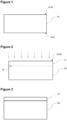
- the figures show a massive substrate 10 of monocrystalline SiC.
- such a substrate has a silicon face 10-Si and a carbon face 10-C.
- GaN epitaxy processes are mainly implemented on the silicon face of SiC. However, it is not excluded to succeed in growing GaN on the carbon face of SiC.
- the orientation of the donor substrate (silicon face / carbon face) during the implementation of the process is chosen according to the face of the SiC intended for the growth of the GaN layer.
- an implantation of ionic species is carried out in the donor substrate 10, so as to form a weakening zone 12 delimiting a thin layer 11 of monocrystalline SiC.
- the implanted species typically comprise hydrogen and/or helium.
- a person skilled in the art is able to define the required implantation energy and dose.
- the implantation is carried out in the surface layer of monocrystalline SiC of said substrate.
- the implantation of the ionic species is carried out through the silicon face 10-Si of the donor substrate.
- this orientation of the donor substrate makes it possible to obtain, on the surface of the final substrate intended for the growth of the GaN layer, the silicon face of the SiC, which is more favorable.
- the implantation of the ionic species must be carried out through the carbon face 10-C of the donor substrate.
- the thin layer 11 of monocrystalline SiC has a thickness of less than 1 ⁇ m.
- a thickness is indeed accessible on an industrial scale with the Smart Cut TM process.
- the implantation devices available in industrial manufacturing lines make it possible to achieve such an implantation depth.
- a first receiving substrate 20 is also provided.
- the main function of said first receiving substrate is to temporarily support the monocrystalline SiC layer 11 between its transfer from the donor substrate and the growth of a semi-insulating SiC layer on the monocrystalline SiC layer.
- the first receiving substrate is chosen to have a coefficient of thermal expansion substantially equal to that of the SiC, so as not to induce stresses or deformations during the epitaxy of the semi-insulating SiC.
- the first receiving substrate and the donor substrate (or the monocrystalline SiC layer in the case of a composite donor substrate) have a difference in coefficient of thermal expansion less than or equal to 3 ⁇ 10 -6 K -1 .
- the first receiving substrate is also made of SiC so as to minimize the difference in coefficient of thermal expansion.
- the first receiving substrate 20 is a SiC substrate having a crystalline quality lower than that of the donor substrate.
- the first receiving substrate can be a polycrystalline SiC substrate, or a monocrystalline SiC substrate but which can include dislocations of all types (unlike the monocrystalline SiC of the donor substrate which is chosen to have an excellent crystalline quality in order to ensure the quality of the GaN epitaxial layer).
- a substrate of lower crystalline quality has the advantage of being less expensive than a substrate of the same quality as the donor substrate, while being perfectly suited to the temporary support function.
- the donor substrate 10 comprising the thin layer 11 of monocrystalline SiC is bonded to the first receiving substrate 20.
- a bonding layer 21 is formed at the interface between said substrates.
- the bonding layer 21 is formed on the first receiving substrate 20, but, in other embodiments not illustrated, the bonding layer can be formed on the donor substrate (on the side of the thin layer 11), or partly on the donor substrate and partly on the first receiving substrate.
- the bonding layer is formed of a thermally stable material during the subsequent epitaxial growth of the semi-insulating SiC on the thin layer 11.
- the material of the bonding layer is chosen so as not to degrade or dissociate at such a temperature.
- the material of the bonding layer is capable of being removed from the interface between the transferred monocrystalline SiC layer and the first receiving substrate 20, for example by means of selective etching, possibly plasma-assisted.
- the bonding layer is a layer of silicon nitride or gallium nitride. The thickness of said layer is typically between 10 nm and a few hundred nanometers.
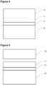
- the donor substrate is detached along the weakening zone 12.
- the detachment can be caused by a heat treatment, a mechanical action, or a combination of these means. This detachment has the effect of transferring the thin layer 11 of monocrystalline SiC onto the first receiving substrate 20.
- the remainder 10' of the donor substrate can optionally be recycled for another use.
- the free face of the transferred monocrystalline SiC layer 11 is the carbon face 11-C (the silicon face 11-Si being on the side of the bonding interface).
- This face is polished, for example by chemical mechanical polishing (CMP) to remove the defects related to the implantation of ionic species and reduce the roughness of the layer 11.
- CMP chemical mechanical polishing
- epitaxial growth of a layer 30 of semi-insulating SiC is carried out on the thin layer 11 of monocrystalline SiC.
- the polytype of the semi-insulating SiC is advantageously identical to that of the SiC of the donor substrate.
- This epitaxial growth is carried out at a very high temperature, generally greater than 1500°C but, as explained above, the bonding layer 21 is stable at this temperature.
- the bonding layer 21 is stable at this temperature.
- the SiC layer is doped with vanadium during its epitaxial growth.
- silicon, carbon and vanadium are deposited simultaneously, using suitable precursors in an epitaxial frame.
- the semi-insulating SiC layer advantageously has a thickness greater than 1 ⁇ m, so as to contribute significantly to heat dissipation within the final structure. This thickness is greater than the thickness directly accessible by the Smart Cut TM process with industrially available equipment.
- the method of transferring a layer of monocrystalline SiC with a thickness of less than 1 ⁇ m and then forming a monocrystalline layer of monocrystalline SiC by epitaxy on said transferred layer makes it possible to circumvent the technical limitations of the implantation equipment available industrially for implementing the Smart Cut TM method. Furthermore, this method does not require a donor substrate made of semi-insulating SiC (which would be particularly expensive); in fact, since the transferred layer essentially has a seed layer function for forming the heat dissipation layer made of semi-insulating SiC, the use of monocrystalline SiC of standard electrical resistivity to form the transferred layer is sufficient.
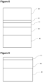
- a second receiving substrate 40 having a high electrical resistivity is provided and bonded to the semi-insulating SiC layer 30.
- the second receiving substrate may be a silicon substrate having an electrical resistivity greater than or equal to 100 ⁇ .cm, a polycrystalline SiC substrate or a polycrystalline AIN substrate, also having an electrical resistivity greater than or equal to 100 ⁇ .cm.
- the thickness of the semi-insulating SiC layer 30 may be adapted.
- the semi-insulating SiC layer 30 will advantageously have a thickness of between 1 and 5 ⁇ m.
- the second receiving substrate is a polycrystalline SiC or polycrystalline AlN substrate, it may be advantageous to form the semi-insulating SiC layer 30 over a much greater thickness. larger, up to 80 ⁇ m, for example of the order of 50 to 80 ⁇ m, to improve heat dissipation within the final structure.
- At least a portion of the bonding layer 21 is then removed, so as to detach the first receiving substrate from the remainder of the structure. During this removal, the layer 21 must be sufficiently damaged to allow dissociation of the structure. Any suitable means may be used. For example, but in a non-limiting manner, the removal of the bonding layer may be carried out by chemical etching, laser delamination and/or the application of mechanical stress.
- the exposed face is the silicon face of the semi-insulating SiC, which is favorable for the epitaxial growth of GaN.
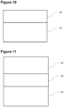
- a layer 50 of GaN (or, as mentioned above, of AlGaN or InGaN) is grown on the free face of the semi-insulating SiC layer 30.
- the thickness of the layer 50 is typically between 1 and 2 ⁇ m.
- a heterojunction is formed by growing by epitaxy, on layer 50, a layer 60 of a III-N alloy different from that of layer 50.
- transistors in particular HEMT transistors, from this heterojunction, by methods known to those skilled in the art, the channel of the transistor being formed at the heterojunction, and the source, drain and gate of the transistor being formed on the channel.
- the structure thus obtained is particularly interesting in that it comprises a relatively thick layer of semi-insulating SiC, which on the one hand serves as a seed for the epitaxial growth of the III-N alloy layer and which on the other hand provides good heat dissipation and a limitation of RF losses. Furthermore, the second receiving substrate, which supports the semi-insulating SiC layer, is directly in contact with said layer, so that the structure does not have a thermal barrier.
- a HEMT or other high-frequency, high-power electronic device formed in a II-N alloy layer grown epitaxially on such a structure exhibits minimized RF losses and maximized heat dissipation.
Landscapes
- Chemical & Material Sciences (AREA)
- Engineering & Computer Science (AREA)
- Crystallography & Structural Chemistry (AREA)
- Materials Engineering (AREA)
- Metallurgy (AREA)
- Organic Chemistry (AREA)
- Inorganic Chemistry (AREA)
- Chemical Kinetics & Catalysis (AREA)
- General Chemical & Material Sciences (AREA)
- Recrystallisation Techniques (AREA)
- Crystals, And After-Treatments Of Crystals (AREA)
- Junction Field-Effect Transistors (AREA)
Claims (15)
- Verfahren zur Herstellung eines Substrats für das epitaktische Wachstum einer Schicht aus Galliumnitrid (GaN), Galliumaluminiumnitrid (AlGaN) oder aus Galliumindiumnitrid (InGaN), das die folgenden aufeinanderfolgenden Schritte umfasst:- Bereitstellen eines Donorsubstrats (10) aus monokristallinem Siliciumkarbid,- Implantieren von ionischen Spezies in das Donorsubstrat (10), so dass eine Schwächungszone (12) gebildet wird, die eine dünne Schicht (11) aus zu übertragendem monokristallinem SiC begrenzt,- Verkleben des Donorsubstrats (10) auf einem ersten Empfängersubstrat (20) anhand einer Verklebungsschicht (21),- Ablösen des Donorsubstrats (10) entlang der Schwächungszone (12), so dass die dünne Schicht (11) aus SiC auf das erste Empfängersubstrat (20) übertragen wird,- epitaktisches Wachstum einer Schicht (30) aus halbisolierendem SiC mit einer Dicke von mehr als 1 µm auf der dünnen Schicht (11) aus SiC,- Verkleben der Schicht (30) aus halbisolierendem SiC mit einem zweiten Empfängersubstrat (40), wobei das zweite Empfängersubstrat (40) einen hohen spezifischen elektrischen Widerstand aufweist,- Entfernen von mindestens einem Teil der Verklebungsschicht (21), um das erste Empfängersubstrat (20) zu abzulösen,- Entfernen der übertragenen dünnen Schicht (11) aus monokristallinem SiC, so dass die Schicht (30) aus halbisolierendem SiC freigelegt wird.
- Verfahren nach Anspruch 1, wobei das erste Empfängersubstrat (20) und das Donorsubstrat (10) einen Unterschied im thermischen Ausdehnungskoeffizienten von weniger als oder gleich 3×10⁻⁶ K-1 aufweisen.
- Verfahren nach einem der Ansprüche 1 oder 2, wobei das erste Empfängersubstrat (20) ein SiC-Substrat ist, das eine geringere Kristallqualität als das Donorsubstrat aufweist.
- Verfahren nach einem der Ansprüche 1 bis 3, wobei die Verklebungsschicht (21) aus einem während des epitaktischen Wachstums der Schicht (30) aus halbisolierenden SiC aus thermisch stabilem Material gebildet wird und geeignet ist, von der Grenzfläche zwischen der übertragenen Schicht (11) aus monokristallinen SiC und dem ersten Empfängersubstrat (20) entfernt zu werden.
- Verfahren nach einem der Ansprüche 1 bis 4, wobei die Verklebungsschicht (21) eine Schicht aus Siliciumnitrid oder Galliumnitrid ist.
- Verfahren nach einem der Ansprüche 1 bis 5, wobei das Entfernen von mindestens einem Teil der Verklebungsschicht (21) chemisches Ätzen, Laser-Delaminieren und/oder die Anwendung von mechanischer Belastung umfasst.
- Verfahren nach einem der Ansprüche 1 bis 6, wobei die Schicht (30) aus halbisolierendem SiC durch Vanadiumdotierung während des epitaktischen Wachstums des SiC oder durch gleichzeitiges Aufbringen von Silicium, Kohlenstoff und Vanadium gebildet wird.
- Verfahren nach einem der Ansprüche 1 bis 7, wobei das zweite Empfängersubstrat (40) ein Siliciumsubstrat mit einem spezifischen elektrischen Widerstand von 100 Q.cm oder mehr ist und wobei die epitaktische Schicht (30) aus halbisolierendem SiC eine Dicke zwischen 1 und 5 µm aufweist.
- Verfahren nach einem der Ansprüche 1 bis 8, wobei das zweite Empfängersubstrat (40) ein polykristallines SiC-Substrat oder ein polykristallines AIN-Substrat mit einem spezifischen elektrischen Widerstand von 100 Q.cm oder mehr ist.
- Verfahren nach Anspruch 9, wobei die epitaktische Schicht (30) aus halbisolierendem SiC eine Dicke von 80 µm oder weniger aufweist.
- Verfahren nach einem der Ansprüche 1 bis 10, das ferner einen Schritt umfasst, bei dem der von der übertragenen Schicht (11) abgelöste Abschnitt (10') des Donorsubstrats recycelt wird, um ein neues Donorsubstrat zu bilden.
- Verfahren nach einem der Ansprüche 1 bis 11, wobei:- die Implantation der ionischen Spezies durch die Siliciumseite (10-Si) des Donorsubstrats (10) hindurch erfolgt,- die Siliciumseite (10-Si) des Donorsubstrats (10) auf dem ersten Empfängersubstrat (20) verklebt wird,so dass nach dem Entfernen der übertragenen dünnen Schicht (11) aus monokristallinem SiC die Siliciumseite der Schicht (30) aus halbisolierendem SiC freigelegt wird.
- Verfahren zur epitaktischen Herstellung einer Schicht aus Galliumnitrid, umfassend:- die Bereitstellung eines Substrats, das anhand des Verfahrens nach einem der Ansprüche 1 bis 12 hergestellt wurde,- das epitaktische Wachstum der Schicht (50) aus Galliumnitrid auf der Schicht (30) aus halbisolierendem SiC des Substrats.
- Verfahren nach Anspruch 13, wobei die Schicht (50) aus Galliumnitrid eine Dicke zwischen 1 und 2 µm aufweist.
- Verfahren zur Herstellung eines Transistors mit hoher Elektronenbeweglichkeit (HEMT), umfassend:- die epitaktische Herstellung einer Schicht (50) aus Galliumnitrid, Galliumaluminiumnitrid oder Galliumindiumnitrid anhand des Verfahrens nach einem der Ansprüche 13 oder 14,- die Bildung eines Heteroübergangs durch Epitaxie einer Schicht (60) aus einem III-N-Material, das sich von dem Material der Schicht (50) unterscheidet, auf der Schicht (50),- die Bildung eines Transistorkanals im Bereich des Heteroübergangs,- die Bildung einer Source, eines Drains und eines Gates des Transistors auf dem Kanal.
Applications Claiming Priority (2)
| Application Number | Priority Date | Filing Date | Title |
|---|---|---|---|
| FR2010209A FR3114912B1 (fr) | 2020-10-06 | 2020-10-06 | Procédé de fabrication d’un substrat pour la croissance épitaxiale d’une couche d’un alliage III-N à base de gallium |
| PCT/FR2021/051708 WO2022074317A1 (fr) | 2020-10-06 | 2021-10-04 | Procédé de fabrication d'un substrat pour la croissance épitaxiale d'une couche d'un alliage iii-n à base de gallium |
Publications (3)
| Publication Number | Publication Date |
|---|---|
| EP4226416A1 EP4226416A1 (de) | 2023-08-16 |
| EP4226416C0 EP4226416C0 (de) | 2024-10-23 |
| EP4226416B1 true EP4226416B1 (de) | 2024-10-23 |
Family
ID=74183299
Family Applications (1)
| Application Number | Title | Priority Date | Filing Date |
|---|---|---|---|
| EP21801584.0A Active EP4226416B1 (de) | 2020-10-06 | 2021-10-04 | Verfahren zur herstellung eines substrats für das epitaktische wachstum einer schicht aus einer galliumbasierten iii-n-legierung |
Country Status (8)
| Country | Link |
|---|---|
| US (1) | US12270123B2 (de) |
| EP (1) | EP4226416B1 (de) |
| JP (1) | JP7791179B2 (de) |
| KR (1) | KR102882310B1 (de) |
| CN (1) | CN116420215A (de) |
| FR (1) | FR3114912B1 (de) |
| TW (1) | TWI908845B (de) |
| WO (1) | WO2022074317A1 (de) |
Families Citing this family (4)
| Publication number | Priority date | Publication date | Assignee | Title |
|---|---|---|---|---|
| FR3151699A1 (fr) * | 2023-07-25 | 2025-01-31 | Commissariat à l'Energie Atomique et aux Energies Alternatives | Procede de realisation d’un substrat multi-materiaux |
| FR3151701A1 (fr) * | 2023-07-28 | 2025-01-31 | Soitec | Substrat semiconducteur détachable en carbure de silicium polycristallin |
| US20250194190A1 (en) * | 2023-12-12 | 2025-06-12 | Wolfspeed, Inc. | Substrates for Power Semiconductor Devices |
| CN118824845B (zh) * | 2024-09-18 | 2024-11-22 | 山东大学 | 一种碳化硅功率器件及其制备方法和应用 |
Family Cites Families (15)
| Publication number | Priority date | Publication date | Assignee | Title |
|---|---|---|---|---|
| FR2816445B1 (fr) * | 2000-11-06 | 2003-07-25 | Commissariat Energie Atomique | Procede de fabrication d'une structure empilee comprenant une couche mince adherant a un substrat cible |
| FR2840731B3 (fr) * | 2002-06-11 | 2004-07-30 | Soitec Silicon On Insulator | Procede de fabrication d'un substrat comportant une couche utile en materiau semi-conducteur monocristallin de proprietes ameliorees |
| FR2817394B1 (fr) * | 2000-11-27 | 2003-10-31 | Soitec Silicon On Insulator | Procede de fabrication d'un substrat notamment pour l'optique, l'electronique ou l'optoelectronique et substrat obtenu par ce procede |
| US6474759B2 (en) * | 2001-02-09 | 2002-11-05 | L & F Platics Co., Ltd. | Cabinet |
| FR2835095B1 (fr) | 2002-01-22 | 2005-03-18 | Procede de preparation d'ensembles a semi-conducteurs separables, notamment pour former des substrats pour l'electronique, l'optoelectrique et l'optique | |
| FR2844095B1 (fr) | 2002-09-03 | 2005-01-28 | Commissariat Energie Atomique | Procede de fabrication d'un substrat composite du type sicoi comprenant une etape d'epitaxie |
| FR2857982B1 (fr) | 2003-07-24 | 2007-05-18 | Soitec Silicon On Insulator | Procede de fabrication d'une couche epitaxiee |
| US7033912B2 (en) * | 2004-01-22 | 2006-04-25 | Cree, Inc. | Silicon carbide on diamond substrates and related devices and methods |
| FR2877491B1 (fr) * | 2004-10-29 | 2007-01-19 | Soitec Silicon On Insulator | Structure composite a forte dissipation thermique |
| JP5436819B2 (ja) | 2008-08-04 | 2014-03-05 | 日本碍子株式会社 | 高周波用半導体素子、高周波用半導体素子形成用のエピタキシャル基板、および高周波用半導体素子形成用エピタキシャル基板の作製方法 |
| US9761493B2 (en) * | 2014-01-24 | 2017-09-12 | Rutgers, The State University Of New Jersey | Thin epitaxial silicon carbide wafer fabrication |
| KR20160044676A (ko) * | 2014-10-15 | 2016-04-26 | 에스케이이노베이션 주식회사 | 탄화규소 기판의 제조방법 |
| JP2016139655A (ja) | 2015-01-26 | 2016-08-04 | 富士通株式会社 | 半導体装置及び半導体装置の製造方法 |
| JP6898222B2 (ja) | 2017-12-27 | 2021-07-07 | エア・ウォーター株式会社 | 化合物半導体基板 |
| FR3114909B1 (fr) * | 2020-10-06 | 2023-03-17 | Soitec Silicon On Insulator | Procédé de fabrication d’un substrat pour la croissance épitaxiale d’une couche d’un alliage III-N à base de gallium |
-
2020
- 2020-10-06 FR FR2010209A patent/FR3114912B1/fr active Active
-
2021
- 2021-08-02 TW TW110128372A patent/TWI908845B/zh active
- 2021-10-04 US US18/247,859 patent/US12270123B2/en active Active
- 2021-10-04 CN CN202180065484.6A patent/CN116420215A/zh active Pending
- 2021-10-04 JP JP2023518171A patent/JP7791179B2/ja active Active
- 2021-10-04 WO PCT/FR2021/051708 patent/WO2022074317A1/fr not_active Ceased
- 2021-10-04 KR KR1020237015259A patent/KR102882310B1/ko active Active
- 2021-10-04 EP EP21801584.0A patent/EP4226416B1/de active Active
Also Published As
| Publication number | Publication date |
|---|---|
| FR3114912B1 (fr) | 2022-09-02 |
| WO2022074317A1 (fr) | 2022-04-14 |
| JP2023544984A (ja) | 2023-10-26 |
| TWI908845B (zh) | 2025-12-21 |
| FR3114912A1 (fr) | 2022-04-08 |
| EP4226416C0 (de) | 2024-10-23 |
| US20230374701A1 (en) | 2023-11-23 |
| CN116420215A (zh) | 2023-07-11 |
| EP4226416A1 (de) | 2023-08-16 |
| TW202215503A (zh) | 2022-04-16 |
| JP7791179B2 (ja) | 2025-12-23 |
| KR20230080475A (ko) | 2023-06-07 |
| US12270123B2 (en) | 2025-04-08 |
| KR102882310B1 (ko) | 2025-11-07 |
Similar Documents
| Publication | Publication Date | Title |
|---|---|---|
| EP1344246B1 (de) | Verfahren zur herstellung eines substrats insbesondere für die optik, elektronik oder optoelektronik und resultierendes substrat | |
| WO2022074317A1 (fr) | Procédé de fabrication d'un substrat pour la croissance épitaxiale d'une couche d'un alliage iii-n à base de gallium | |
| WO2006000691A1 (fr) | Support d'epitaxie hybride et son procede de fabrication | |
| EP4128329B1 (de) | Verfahren zur herstellung einer verbundstruktur mit einer dünnen schicht aus monokristallinem sic auf einem trägersubstrat aus sic | |
| FR3103962A1 (fr) | Procede de fabrication d’une structure composite comprenant une couche mince en sic monocristallin sur un substrat support en sic cristallin | |
| FR2857983A1 (fr) | Procede de fabrication d'une couche epitaxiee | |
| FR2835096A1 (fr) | Procede de fabrication d'un substrat auto-porte en materiau semi-conducteur monocristallin | |
| EP4226409A1 (de) | Verfahren zur herstellung eines substrats für epitaktisches wachstum einer galliumbasierten iii-n-legierungsschicht | |
| TW201413783A (zh) | 碳化矽紋層 | |
| FR3114910A1 (fr) | Procédé de fabrication d’un substrat pour la croissance épitaxiale d’une couche d’un alliage III-N à base de gallium | |
| EP4226417A1 (de) | Verfahren zur herstellung eines substrats für das epitaktische wachstum einer schicht aus einer galliumbasierten iii-n-legierung | |
| JP5598321B2 (ja) | 半導体デバイスの製造方法 | |
| FR2905799A1 (fr) | Realisation d'un substrat en gan | |
| EP4449477B1 (de) | Verfahren zur herstellung einer halbleiterstruktur mit einem polykristallinen siliciumcarbidsubstrat und einer aktiven schicht aus einkristallinem siliciumcarbid | |
| EP4016585B1 (de) | Elektronische vorrichtung aus siliciumcarbid und ihr herstellungsverfahren | |
| WO2025186045A1 (fr) | Procédé de préparation d'un substrat support en matériau polycristallin et procédé de fabrication d'une structure composite incluant ledit substrat support | |
| WO2025186046A1 (fr) | Procédé de préparation d'un substrat support en matériau polycristallin et procédé de fabrication d'une structure composite incluant ledit substrat support | |
| FR3154229A1 (fr) | Procédé de croissance d’un matériau III-N | |
| FR2971620A1 (fr) | Substrat semi-conducteur a couche d'epitaxie épaisse, et procédé de fabrication | |
| FR3166240A1 (fr) | Substrat intermediaire pour la fabrication d’un substrat pour transistor a haute mobilite d’electrons | |
| FR3159854A1 (fr) | Structure à hétérojonction pour un transistor à haute mobilité électronique | |
| EP4716960A1 (de) | Verfahren zur doppelschichtübertragung | |
| FR3143044A1 (fr) | Structure comprenant une couche d’arseniure de bore de haute conductivite thermique et procede de fabrication | |
| WO2023052704A1 (fr) | Procédé de fabrication d'une structure composite comprenant une couche mince en sic monocristallin sur un substrat support en sic polycristallin |
Legal Events
| Date | Code | Title | Description |
|---|---|---|---|
| STAA | Information on the status of an ep patent application or granted ep patent |
Free format text: STATUS: UNKNOWN |
|
| STAA | Information on the status of an ep patent application or granted ep patent |
Free format text: STATUS: THE INTERNATIONAL PUBLICATION HAS BEEN MADE |
|
| PUAI | Public reference made under article 153(3) epc to a published international application that has entered the european phase |
Free format text: ORIGINAL CODE: 0009012 |
|
| STAA | Information on the status of an ep patent application or granted ep patent |
Free format text: STATUS: REQUEST FOR EXAMINATION WAS MADE |
|
| 17P | Request for examination filed |
Effective date: 20230504 |
|
| AK | Designated contracting states |
Kind code of ref document: A1 Designated state(s): AL AT BE BG CH CY CZ DE DK EE ES FI FR GB GR HR HU IE IS IT LI LT LU LV MC MK MT NL NO PL PT RO RS SE SI SK SM TR |
|
| DAV | Request for validation of the european patent (deleted) | ||
| DAX | Request for extension of the european patent (deleted) | ||
| REG | Reference to a national code |
Ref country code: DE Ref legal event code: R079 Free format text: PREVIOUS MAIN CLASS: H01L0021762000 Ipc: H01L0021020000 Ref country code: DE Ref legal event code: R079 Ref document number: 602021020748 Country of ref document: DE Free format text: PREVIOUS MAIN CLASS: H01L0021762000 Ipc: H01L0021020000 |
|
| GRAP | Despatch of communication of intention to grant a patent |
Free format text: ORIGINAL CODE: EPIDOSNIGR1 |
|
| STAA | Information on the status of an ep patent application or granted ep patent |
Free format text: STATUS: GRANT OF PATENT IS INTENDED |
|
| RIC1 | Information provided on ipc code assigned before grant |
Ipc: H01L 21/762 20060101ALI20240502BHEP Ipc: H01L 21/02 20060101AFI20240502BHEP |
|
| INTG | Intention to grant announced |
Effective date: 20240605 |
|
| GRAS | Grant fee paid |
Free format text: ORIGINAL CODE: EPIDOSNIGR3 |
|
| GRAA | (expected) grant |
Free format text: ORIGINAL CODE: 0009210 |
|
| STAA | Information on the status of an ep patent application or granted ep patent |
Free format text: STATUS: THE PATENT HAS BEEN GRANTED |
|
| AK | Designated contracting states |
Kind code of ref document: B1 Designated state(s): AL AT BE BG CH CY CZ DE DK EE ES FI FR GB GR HR HU IE IS IT LI LT LU LV MC MK MT NL NO PL PT RO RS SE SI SK SM TR |
|
| REG | Reference to a national code |
Ref country code: GB Ref legal event code: FG4D Free format text: NOT ENGLISH |
|
| REG | Reference to a national code |
Ref country code: CH Ref legal event code: EP |
|
| REG | Reference to a national code |
Ref country code: DE Ref legal event code: R096 Ref document number: 602021020748 Country of ref document: DE |
|
| REG | Reference to a national code |
Ref country code: IE Ref legal event code: FG4D Free format text: LANGUAGE OF EP DOCUMENT: FRENCH |
|
| U01 | Request for unitary effect filed |
Effective date: 20241114 |
|
| U07 | Unitary effect registered |
Designated state(s): AT BE BG DE DK EE FI FR IT LT LU LV MT NL PT RO SE SI Effective date: 20241121 |
|
| PG25 | Lapsed in a contracting state [announced via postgrant information from national office to epo] |
Ref country code: IS Free format text: LAPSE BECAUSE OF FAILURE TO SUBMIT A TRANSLATION OF THE DESCRIPTION OR TO PAY THE FEE WITHIN THE PRESCRIBED TIME-LIMIT Effective date: 20250223 Ref country code: HR Free format text: LAPSE BECAUSE OF FAILURE TO SUBMIT A TRANSLATION OF THE DESCRIPTION OR TO PAY THE FEE WITHIN THE PRESCRIBED TIME-LIMIT Effective date: 20241023 |
|
| PG25 | Lapsed in a contracting state [announced via postgrant information from national office to epo] |
Ref country code: ES Free format text: LAPSE BECAUSE OF FAILURE TO SUBMIT A TRANSLATION OF THE DESCRIPTION OR TO PAY THE FEE WITHIN THE PRESCRIBED TIME-LIMIT Effective date: 20241023 |
|
| PG25 | Lapsed in a contracting state [announced via postgrant information from national office to epo] |
Ref country code: NO Free format text: LAPSE BECAUSE OF FAILURE TO SUBMIT A TRANSLATION OF THE DESCRIPTION OR TO PAY THE FEE WITHIN THE PRESCRIBED TIME-LIMIT Effective date: 20250123 |
|
| PG25 | Lapsed in a contracting state [announced via postgrant information from national office to epo] |
Ref country code: GR Free format text: LAPSE BECAUSE OF FAILURE TO SUBMIT A TRANSLATION OF THE DESCRIPTION OR TO PAY THE FEE WITHIN THE PRESCRIBED TIME-LIMIT Effective date: 20250124 |
|
| PG25 | Lapsed in a contracting state [announced via postgrant information from national office to epo] |
Ref country code: PL Free format text: LAPSE BECAUSE OF FAILURE TO SUBMIT A TRANSLATION OF THE DESCRIPTION OR TO PAY THE FEE WITHIN THE PRESCRIBED TIME-LIMIT Effective date: 20241023 |
|
| PG25 | Lapsed in a contracting state [announced via postgrant information from national office to epo] |
Ref country code: RS Free format text: LAPSE BECAUSE OF FAILURE TO SUBMIT A TRANSLATION OF THE DESCRIPTION OR TO PAY THE FEE WITHIN THE PRESCRIBED TIME-LIMIT Effective date: 20250123 |
|
| PG25 | Lapsed in a contracting state [announced via postgrant information from national office to epo] |
Ref country code: SM Free format text: LAPSE BECAUSE OF FAILURE TO SUBMIT A TRANSLATION OF THE DESCRIPTION OR TO PAY THE FEE WITHIN THE PRESCRIBED TIME-LIMIT Effective date: 20241023 |
|
| PG25 | Lapsed in a contracting state [announced via postgrant information from national office to epo] |
Ref country code: SK Free format text: LAPSE BECAUSE OF FAILURE TO SUBMIT A TRANSLATION OF THE DESCRIPTION OR TO PAY THE FEE WITHIN THE PRESCRIBED TIME-LIMIT Effective date: 20241023 |
|
| PG25 | Lapsed in a contracting state [announced via postgrant information from national office to epo] |
Ref country code: CZ Free format text: LAPSE BECAUSE OF FAILURE TO SUBMIT A TRANSLATION OF THE DESCRIPTION OR TO PAY THE FEE WITHIN THE PRESCRIBED TIME-LIMIT Effective date: 20241023 |
|
| PLBE | No opposition filed within time limit |
Free format text: ORIGINAL CODE: 0009261 |
|
| STAA | Information on the status of an ep patent application or granted ep patent |
Free format text: STATUS: NO OPPOSITION FILED WITHIN TIME LIMIT |
|
| 26N | No opposition filed |
Effective date: 20250724 |
|
| U20 | Renewal fee for the european patent with unitary effect paid |
Year of fee payment: 5 Effective date: 20250909 |
|
| PGFP | Annual fee paid to national office [announced via postgrant information from national office to epo] |
Ref country code: GB Payment date: 20250904 Year of fee payment: 5 |
|
| PGFP | Annual fee paid to national office [announced via postgrant information from national office to epo] |
Ref country code: IE Payment date: 20250909 Year of fee payment: 5 |