EP4207310A1 - Vertical semiconductor device with improved ruggedness - Google Patents
Vertical semiconductor device with improved ruggedness Download PDFInfo
- Publication number
- EP4207310A1 EP4207310A1 EP23151813.5A EP23151813A EP4207310A1 EP 4207310 A1 EP4207310 A1 EP 4207310A1 EP 23151813 A EP23151813 A EP 23151813A EP 4207310 A1 EP4207310 A1 EP 4207310A1
- Authority
- EP
- European Patent Office
- Prior art keywords
- buffer layer
- doping
- layer
- doping concentration
- substrate
- Prior art date
- Legal status (The legal status is an assumption and is not a legal conclusion. Google has not performed a legal analysis and makes no representation as to the accuracy of the status listed.)
- Pending
Links
Images




Classifications
-
- H—ELECTRICITY
- H10—SEMICONDUCTOR DEVICES; ELECTRIC SOLID-STATE DEVICES NOT OTHERWISE PROVIDED FOR
- H10D—INORGANIC ELECTRIC SEMICONDUCTOR DEVICES
- H10D84/00—Integrated devices formed in or on semiconductor substrates that comprise only semiconducting layers, e.g. on Si wafers or on GaAs-on-Si wafers
- H10D84/101—Integrated devices comprising main components and built-in components, e.g. IGBT having built-in freewheel diode
- H10D84/141—VDMOS having built-in components
- H10D84/146—VDMOS having built-in components the built-in components being Schottky barrier diodes
-
- H—ELECTRICITY
- H10—SEMICONDUCTOR DEVICES; ELECTRIC SOLID-STATE DEVICES NOT OTHERWISE PROVIDED FOR
- H10D—INORGANIC ELECTRIC SEMICONDUCTOR DEVICES
- H10D12/00—Bipolar devices controlled by the field effect, e.g. insulated-gate bipolar transistors [IGBT]
- H10D12/01—Manufacture or treatment
- H10D12/031—Manufacture or treatment of IGBTs
-
- H—ELECTRICITY
- H10—SEMICONDUCTOR DEVICES; ELECTRIC SOLID-STATE DEVICES NOT OTHERWISE PROVIDED FOR
- H10D—INORGANIC ELECTRIC SEMICONDUCTOR DEVICES
- H10D30/00—Field-effect transistors [FET]
- H10D30/01—Manufacture or treatment
- H10D30/021—Manufacture or treatment of FETs having insulated gates [IGFET]
- H10D30/028—Manufacture or treatment of FETs having insulated gates [IGFET] of double-diffused metal oxide semiconductor [DMOS] FETs
- H10D30/0291—Manufacture or treatment of FETs having insulated gates [IGFET] of double-diffused metal oxide semiconductor [DMOS] FETs of vertical DMOS [VDMOS] FETs
-
- H—ELECTRICITY
- H10—SEMICONDUCTOR DEVICES; ELECTRIC SOLID-STATE DEVICES NOT OTHERWISE PROVIDED FOR
- H10D—INORGANIC ELECTRIC SEMICONDUCTOR DEVICES
- H10D30/00—Field-effect transistors [FET]
- H10D30/60—Insulated-gate field-effect transistors [IGFET]
- H10D30/64—Double-diffused metal-oxide semiconductor [DMOS] FETs
- H10D30/66—Vertical DMOS [VDMOS] FETs
-
- H—ELECTRICITY
- H10—SEMICONDUCTOR DEVICES; ELECTRIC SOLID-STATE DEVICES NOT OTHERWISE PROVIDED FOR
- H10D—INORGANIC ELECTRIC SEMICONDUCTOR DEVICES
- H10D62/00—Semiconductor bodies, or regions thereof, of devices having potential barriers
- H10D62/10—Shapes, relative sizes or dispositions of the regions of the semiconductor bodies; Shapes of the semiconductor bodies
- H10D62/102—Constructional design considerations for preventing surface leakage or controlling electric field concentration
- H10D62/103—Constructional design considerations for preventing surface leakage or controlling electric field concentration for increasing or controlling the breakdown voltage of reverse-biased devices
- H10D62/105—Constructional design considerations for preventing surface leakage or controlling electric field concentration for increasing or controlling the breakdown voltage of reverse-biased devices by having particular doping profiles, shapes or arrangements of PN junctions; by having supplementary regions, e.g. junction termination extension [JTE]
- H10D62/106—Constructional design considerations for preventing surface leakage or controlling electric field concentration for increasing or controlling the breakdown voltage of reverse-biased devices by having particular doping profiles, shapes or arrangements of PN junctions; by having supplementary regions, e.g. junction termination extension [JTE] having supplementary regions doped oppositely to or in rectifying contact with regions of the semiconductor bodies, e.g. guard rings with PN or Schottky junctions
-
- H—ELECTRICITY
- H10—SEMICONDUCTOR DEVICES; ELECTRIC SOLID-STATE DEVICES NOT OTHERWISE PROVIDED FOR
- H10D—INORGANIC ELECTRIC SEMICONDUCTOR DEVICES
- H10D62/00—Semiconductor bodies, or regions thereof, of devices having potential barriers
- H10D62/10—Shapes, relative sizes or dispositions of the regions of the semiconductor bodies; Shapes of the semiconductor bodies
- H10D62/129—Cathode regions of diodes
-
- H—ELECTRICITY
- H10—SEMICONDUCTOR DEVICES; ELECTRIC SOLID-STATE DEVICES NOT OTHERWISE PROVIDED FOR
- H10D—INORGANIC ELECTRIC SEMICONDUCTOR DEVICES
- H10D62/00—Semiconductor bodies, or regions thereof, of devices having potential barriers
- H10D62/10—Shapes, relative sizes or dispositions of the regions of the semiconductor bodies; Shapes of the semiconductor bodies
- H10D62/13—Semiconductor regions connected to electrodes carrying current to be rectified, amplified or switched, e.g. source or drain regions
- H10D62/149—Source or drain regions of field-effect devices
- H10D62/151—Source or drain regions of field-effect devices of IGFETs
- H10D62/156—Drain regions of DMOS transistors
- H10D62/157—Impurity concentrations or distributions
-
- H—ELECTRICITY
- H10—SEMICONDUCTOR DEVICES; ELECTRIC SOLID-STATE DEVICES NOT OTHERWISE PROVIDED FOR
- H10D—INORGANIC ELECTRIC SEMICONDUCTOR DEVICES
- H10D62/00—Semiconductor bodies, or regions thereof, of devices having potential barriers
- H10D62/10—Shapes, relative sizes or dispositions of the regions of the semiconductor bodies; Shapes of the semiconductor bodies
- H10D62/17—Semiconductor regions connected to electrodes not carrying current to be rectified, amplified or switched, e.g. channel regions
- H10D62/393—Body regions of DMOS transistors or IGBTs
-
- H—ELECTRICITY
- H10—SEMICONDUCTOR DEVICES; ELECTRIC SOLID-STATE DEVICES NOT OTHERWISE PROVIDED FOR
- H10D—INORGANIC ELECTRIC SEMICONDUCTOR DEVICES
- H10D62/00—Semiconductor bodies, or regions thereof, of devices having potential barriers
- H10D62/60—Impurity distributions or concentrations
-
- H—ELECTRICITY
- H10—SEMICONDUCTOR DEVICES; ELECTRIC SOLID-STATE DEVICES NOT OTHERWISE PROVIDED FOR
- H10D—INORGANIC ELECTRIC SEMICONDUCTOR DEVICES
- H10D62/00—Semiconductor bodies, or regions thereof, of devices having potential barriers
- H10D62/80—Semiconductor bodies, or regions thereof, of devices having potential barriers characterised by the materials
- H10D62/83—Semiconductor bodies, or regions thereof, of devices having potential barriers characterised by the materials being Group IV materials, e.g. B-doped Si or undoped Ge
- H10D62/832—Semiconductor bodies, or regions thereof, of devices having potential barriers characterised by the materials being Group IV materials, e.g. B-doped Si or undoped Ge being Group IV materials comprising two or more elements, e.g. SiGe
- H10D62/8325—Silicon carbide
-
- H—ELECTRICITY
- H10—SEMICONDUCTOR DEVICES; ELECTRIC SOLID-STATE DEVICES NOT OTHERWISE PROVIDED FOR
- H10D—INORGANIC ELECTRIC SEMICONDUCTOR DEVICES
- H10D8/00—Diodes
-
- H—ELECTRICITY
- H10—SEMICONDUCTOR DEVICES; ELECTRIC SOLID-STATE DEVICES NOT OTHERWISE PROVIDED FOR
- H10D—INORGANIC ELECTRIC SEMICONDUCTOR DEVICES
- H10D8/00—Diodes
- H10D8/01—Manufacture or treatment
- H10D8/051—Manufacture or treatment of Schottky diodes
-
- H—ELECTRICITY
- H10—SEMICONDUCTOR DEVICES; ELECTRIC SOLID-STATE DEVICES NOT OTHERWISE PROVIDED FOR
- H10D—INORGANIC ELECTRIC SEMICONDUCTOR DEVICES
- H10D8/00—Diodes
- H10D8/60—Schottky-barrier diodes
-
- H—ELECTRICITY
- H10—SEMICONDUCTOR DEVICES; ELECTRIC SOLID-STATE DEVICES NOT OTHERWISE PROVIDED FOR
- H10P—GENERIC PROCESSES OR APPARATUS FOR THE MANUFACTURE OR TREATMENT OF DEVICES COVERED BY CLASS H10
- H10P30/00—Ion implantation into wafers, substrates or parts of devices
- H10P30/20—Ion implantation into wafers, substrates or parts of devices into semiconductor materials, e.g. for doping
- H10P30/202—Ion implantation into wafers, substrates or parts of devices into semiconductor materials, e.g. for doping characterised by the semiconductor materials
- H10P30/204—Ion implantation into wafers, substrates or parts of devices into semiconductor materials, e.g. for doping characterised by the semiconductor materials into Group IV semiconductors
- H10P30/2042—Ion implantation into wafers, substrates or parts of devices into semiconductor materials, e.g. for doping characterised by the semiconductor materials into Group IV semiconductors into crystalline silicon carbide
-
- H—ELECTRICITY
- H10—SEMICONDUCTOR DEVICES; ELECTRIC SOLID-STATE DEVICES NOT OTHERWISE PROVIDED FOR
- H10P—GENERIC PROCESSES OR APPARATUS FOR THE MANUFACTURE OR TREATMENT OF DEVICES COVERED BY CLASS H10
- H10P30/00—Ion implantation into wafers, substrates or parts of devices
- H10P30/20—Ion implantation into wafers, substrates or parts of devices into semiconductor materials, e.g. for doping
- H10P30/21—Ion implantation into wafers, substrates or parts of devices into semiconductor materials, e.g. for doping of electrically active species
Definitions
- the present disclosure relates to vertical semiconductor devices, and in particular to vertical semiconductor devices for power applications with improved ruggedness due to increased radiation tolerance.
- FIG. 1 shows the general structure of a conventional vertical semiconductor device 10.
- the conventional vertical semiconductor device 10 includes a substrate 12 and a drift layer 14 over the substrate 12.
- a graph shows the relative doping concentrations for the substrate 12 and the drift layer 14. As shown, the substrate 12 is much more heavily doped than the drift layer 14.
- Implanted regions, additional semiconductor layers, and/or metal layers may be added to the conventional vertical semiconductor device 10 to provide a PiN diode, a Schottky diode, a MOSFET, or any other type of device.
- the conventional vertical semiconductor device 10 may provide a high blocking voltage and thus may be useful for high power applications as discussed above.
- the conventional vertical semiconductor device 10 may be subject to failure at high blocking voltages due to radiation intolerance.
- a vertical semiconductor device includes a substrate, a buffer layer over the substrate, and a drift layer over the buffer layer.
- the substrate has a first doping type and a first doping concentration.
- the buffer layer has the first doping type and a second doping concentration that is less than the first doping concentration.
- the drift layer has the first doping type and a third doping concentration that is less than the second doping concentration.
- a method includes the steps of providing a substrate, providing a buffer layer over the substrate, and providing a drift layer over the buffer layer.
- the substrate has a first doping type and a first doping concentration.
- the buffer layer has the first doping type and a second doping concentration that is less than the first doping concentration.
- the drift layer has the first doping type and a third doping concentration that is less than the second doping concentration.
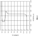
- Figure 2 is a graph illustrating an exemplary relationship between current through the conventional vertical semiconductor device 10 and voltage across the conventional vertical semiconductor device 10.
- the current through the device maintains relatively consistent leakage current at 1 pico-Amps for blocking voltages up to 1600 Volts (this graph is applicable to devices rated for blocking voltages up to 1200 Volts and forward currents up to 50 Amps, similar curves will show the same general characteristics for devices having other ratings).
- the conventional vertical semiconductor device 10 begins to experience avalanche breakdown, and the current through the device thus increases sharply.
- 1 Amps the conventional vertical semiconductor device 10 experiences a second breakdown in which the current through the device continues to increase, and the voltage across the device decreases sharply.
- the extent to which the conventional vertical semiconductor device 10 experiences this second breakdown is proportional to the ability of the device to withstand radiation. This is because when operating at high voltages, radiation particles such as terrestrial neutrons or heavy ions may collide with charge particles in the device, knocking these charge particles loose and causing a cascade effect that results in the device "jumping" from the bottom portion of the curve shown in Figure 2 to the top portion in which second breakdown occurs. If this occurs, the conventional vertical semiconductor device 10 will catastrophically fail.
- Figure 3 shows the basic structure of a vertical semiconductor device 16 according to one embodiment of the present disclosure.
- the vertical semiconductor device 16 includes a substrate 18, a buffer layer 20 over the substrate 18, and a drift layer 22 over the buffer layer 20.
- a graph shows the relative doping concentrations of the substrate 18, the buffer layer 20, and the drift layer 22.
- the substrate 18 is more heavily doped than the buffer layer 20, which is in turn more heavily doped than the drift layer 22.
- the substrate 18, the buffer layer 20, and the drift layer 22 are all doped in a relatively consistent manner and thus form a step doping profile as shown.
- the buffer layer 20 with a doping concentration that is higher than the drift layer 22 but lower than the substrate 18 creates a buffer for charge particles that may be accelerated by collisions with radiated particles, allowing these accelerated charge particles to recombine instead of passing through the vertical semiconductor device 16.
- the thickness and doping concentrations of the substrate 18, the buffer layer 20, and the drift layer 22 are merely exemplary. In particular, these thicknesses and doping concentrations are shown for a device rated for 1200 Volts. Those skilled in the art will readily appreciate that higher blocking voltages may dictate greater thicknesses for the drift layer 22, and in some embodiments, the buffer layer 20, and/or decreased doping concentrations for the same. However, the relationship between the thicknesses and doping concentrations of these layers will remain relatively unchanged. In one embodiment, a thickness of the buffer layer 20 may be between 5% and 35% the thickness of the drift layer 22.
- a thickness of the buffer layer 20 may be between 5% and 10% the thickness of the drift layer 22, between 10% and 15% the thickness of the drift layer 22, between 15% and 20% the thickness of the drift layer 22, between 20% and 25% the thickness of the drift layer, between 25% and 30% the thickness of the drift layer 22, between 30% and 35% the thickness of the drift layer 22, between 15% and 15% the thickness of the drift layer 22, and between 25% and 35% the thickness of the drift layer 22.
- the doping concentration of the buffer layer 20 may vary between 20% and 90% the doping concentration of the substrate 18 while remaining greater than the doping concentration of the drift layer 22 by at least 20%.
- the doping concentration of the buffer layer 20 may be between 20% and 30% the doping concentration of the substrate 18, between 30% and 40% the doping concentration of the substrate 18, between 40% and 50% the doping concentration of the substrate 18, between 50% and 60% the doping concentration of the substrate 18, between 60% and 70% the doping concentration of the substrate 18, between 70% and 80% the doping concentration of the substrate 18, and between 80% and 90% the doping concentration of the substrate 18.
- the substrate 18, the buffer layer 20, and the drift layer 22 are silicon carbide (SiC).
- the buffer layer 20 may be an epitaxial layer that is grown on the substrate 18 before the drift layer 22.
- the drift layer 22 may then be grown over the buffer layer 20.
- the buffer layer 20 may be grown in an environment with dopants to provide the desired doping concentrations, or grown and subsequently implanted (e.g., via ion implantation) to the desired doping concentration.
- the buffer layer 20 may be an implanted region in the surface of the substrate 18.
- the substrate 18 may be doped with an opposite doping type (e.g., if the substrate 18 is an n-type substrate, it may be doped with a p-dopant) to decrease the net doping concentration thereof.
- an opposite doping type e.g., if the substrate 18 is an n-type substrate, it may be doped with a p-dopant
- the principles of the present disclosure apply equally to n-type or p-type substrates, buffer layers, and drift layers. That is, the principles of the present disclosure may be equally applied to n-type and p-type devices.
- Figure 4A is a graph illustrating the effect of the buffer layer 20 on the second breakdown of the vertical semiconductor device 16.
- Figure 4A shows a relationship between current through the vertical semiconductor device 16 and voltage across the vertical semiconductor device 16 for several different thicknesses of the buffer layer 20 at a doping concentration of 10 17 cm -3 .
- the voltage at which second breakdown occurs also increases.
- the second breakdown voltage is the lowest voltage at which the second breakdown occurs, and reflects the left-most point of the upper portion of the graph shown in Figure 4A .
- Increasing the second breakdown voltage may significantly increase the radiation tolerance and thus ruggedness of the vertical semiconductor device 16.
- the buffer layer 20 increases the second breakdown voltage such that it is greater than the avalanche voltage.
- Figure 4B is a graph illustrating the effect of the buffer layer 20 on both the avalanche breakdown voltage and the second breakdown voltage.
- Figure 4B shows a relationship between the avalanche breakdown voltage and the second breakdown voltage to a doping concentration of the buffer layer 20 when the buffer layer is 1 ⁇ m thick.
- the second breakdown voltage similarly increases, up to a certain point, where it begins to decline rapidly.
- the doping concentration of the buffer layer 20 has a minimal effect on the avalanche breakdown voltage, and thus using the buffer layer 20 does not decrease the performance of the vertical semiconductor device 16.
- Figure 4C is a graph illustrating the effect of the buffer layer 20 on the failure rate of the vertical semiconductor device 16.
- Figure 4C shows a relationship between failure rate (as a function of device hours) and voltage across the device.
- a first line shows the failure rate for devices not including the buffer layer 20, while a second line shows the failure rate for devices including the buffer layer 20.
- the failure rate of devices including the buffer layer 20 is significantly lower for a given device voltage.
- Figure 5 shows the vertical semiconductor device 16 according to an additional embodiment of the present disclosure.
- the vertical semiconductor device 16 shown in Figure 5 is substantially similar to that shown in Figure 3 , except for the doping profile of the device and the relative thicknesses of the layers.
- the buffer layer 20 provides a linearly graded doping concentration that decreases in proportion to a distance from the drift layer 22 such that the overall doping profile of the device includes a step between the drift layer 22 and the buffer layer 20 and another step between the buffer layer 20 and the substrate 18.
- the buffer layer 20 may be thicker to allow for the linear transition in the doping profile thereof.
- Such a doping profile may be created by first growing the buffer layer 20 and then performing ion implantation on it, or by growing the buffer layer 20 in an environment wherein the concentration of dopants are controlled throughout the growth process.
- this doping profile is merely exemplary, and any linearly graded doping concentration may be substituted for the one shown in Figure 5 without departing from the principles of the present disclosure.
- Figure 6 shows the vertical semiconductor device 16 according to an additional embodiment of the present disclosure.
- the vertical semiconductor device 16 shown in Figure 6 is substantially similar to that shown in Figure 3 except for the doping profile of the device and the relative thicknesses of the layers.
- the buffer layer 20 provides a substantially smooth transition between the doping concentration of the drift layer 22 and the doping concentration of the substrate 18.
- the buffer layer 20 may be substantially thicker to allow for the transition in the doping profile thereof.
- Such a doping profile may be created by first growing the buffer layer 20 and then performing ion implantation on it, or by growing the buffer layer 20 in an environment wherein the concentration of dopants are controlled throughout the growth process.
- this doping profile is merely exemplary, and any graded doping concentration, linear or otherwise, may be substituted for the one shown in Figure 6 without departing from the principles of the present disclosure.
- FIG. 7 shows the vertical semiconductor device 16 according to an additional embodiment of the present disclosure.
- the vertical semiconductor device 16 shown in Figure 7 is substantially similar to that shown in Figure 3 except for the doping profile of the device and the relative thicknesses of the layers.
- the buffer layer 20 is provided as a doping "spike" and is not directly over the substrate 18.
- the buffer layer 20 may be reduced in thickness.
- Such a doping profile may be formed either via separate growth on top of a small portion of the drift layer 22 or by growing a small portion of the drift layer 22, performing ion implantation to create the buffer layer 20, then growing the rest of the drift layer 22.
- this doping profile is merely exemplary, and any "spike" doping profile may be substituted for the one shown in Figure 7 without departing from the principles of the present disclosure.
- Figure 8 shows the effect of the buffer layer 20 for the embodiments shown in Figures 3 , 5 , 6 and 7 on the second breakdown of the vertical semiconductor device 16.
- the buffer layer 20 significantly increases the second breakdown voltage for each embodiment when compared to a conventional vertical semiconductor device not including the buffer layer 20. As discussed above, this results in a significantly increased radiation tolerance and thus improved ruggedness of the vertical semiconductor device 16.
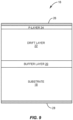
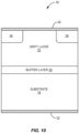
- the vertical semiconductor device 16 is a PiN diode as shown in Figure 9 . Accordingly, the vertical semiconductor device 16 includes a p-layer 24 over the drift layer 22, an anode 26 over the p-layer 24, and a cathode 28 on the substrate 18 opposite the buffer layer 20. In another embodiment, the vertical semiconductor device 16 is a Schottky diode as shown in Figure 10 . Accordingly, the vertical semiconductor device 16 includes an anode 30 over the drift layer 22 and a cathode 32 on the substrate 18 opposite the buffer layer 20.
- the vertical semiconductor device 16 is a MOSFET as shown in Figure 11 . Accordingly, the vertical semiconductor device 16 includes a pair of junction implant regions 36, which are laterally separated from one another and include a source region 36A and a well region 36B, a gate oxide layer 38 running between the junction implant regions 36, a gate contact 40 over the gate oxide layer 38, a pair of source contacts 42 over a portion of the junction implant regions 36, and a drain contact 44 on the substrate 18 opposite the buffer layer 20.
- junction implant regions 36 which are laterally separated from one another and include a source region 36A and a well region 36B, a gate oxide layer 38 running between the junction implant regions 36, a gate contact 40 over the gate oxide layer 38, a pair of source contacts 42 over a portion of the junction implant regions 36, and a drain contact 44 on the substrate 18 opposite the buffer layer 20.
- additional implanted regions, semiconductor layers, and/or metal layers may be provided to provide any number of different types of semiconductor devices, all of which are contemplated herein.
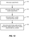
- Figure 12 is a flow diagram illustrating a method for manufacturing a vertical semiconductor device according to one embodiment of the present disclosure.
- a substrate is provided (step 100).
- the substrate may be silicon carbide (SiC) as discussed above, and has a first doping type and a first doping concentration.
- a buffer layer is then provided over the substrate (step 102).
- the buffer layer has the first doping type and a second doping concentration that is less than the first doping concentration.
- the buffer layer may be epitaxially grown in an environment including dopants designed to create a desired doping profile, or may be grown and subsequently implanted (e.g., via ion implantation) to produce the desired doping profile.
- a drift layer is then provided over the buffer layer (step 104).
- the drift layer has the first doping type and a third doping concentration that is less than the second doping concentration.
- the drift layer may be epitaxially grown over the buffer layer.
- one or more additional implanted regions, semiconductor layers, and/or metal layers may be provided in order to provide a semiconductor device of a desired type (step 106).
- a PiN diode, Schottky diode, MOSFET, or any other type of semiconductor device may be created by providing different implanted regions, semiconductor layers, and/or metal layers.
Landscapes
- Electrodes Of Semiconductors (AREA)
Abstract
Description
- The present disclosure relates to vertical semiconductor devices, and in particular to vertical semiconductor devices for power applications with improved ruggedness due to increased radiation tolerance.
- Vertical semiconductor devices come in several varieties, each of which may be used for different applications. One notable use of vertical semiconductor devices is for high power applications. In particular, devices such as PiN diodes, Schottky diodes, and vertical metal-oxide semiconductor field-effect transistors (MOSFETs) may be rated for high blocking voltages and thus are often used for these power applications. For purposes of illustration,
Figure 1 shows the general structure of a conventionalvertical semiconductor device 10. The conventionalvertical semiconductor device 10 includes asubstrate 12 and adrift layer 14 over thesubstrate 12. A graph shows the relative doping concentrations for thesubstrate 12 and thedrift layer 14. As shown, thesubstrate 12 is much more heavily doped than thedrift layer 14. Implanted regions, additional semiconductor layers, and/or metal layers may be added to the conventionalvertical semiconductor device 10 to provide a PiN diode, a Schottky diode, a MOSFET, or any other type of device. When finished, the conventionalvertical semiconductor device 10 may provide a high blocking voltage and thus may be useful for high power applications as discussed above. However, the conventionalvertical semiconductor device 10 may be subject to failure at high blocking voltages due to radiation intolerance. - The present disclosure relates to vertical semiconductor devices, and in particular to vertical semiconductor devices for power applications with improved ruggedness due to increased radiation tolerance. In one embodiment, a vertical semiconductor device includes a substrate, a buffer layer over the substrate, and a drift layer over the buffer layer. The substrate has a first doping type and a first doping concentration. The buffer layer has the first doping type and a second doping concentration that is less than the first doping concentration. The drift layer has the first doping type and a third doping concentration that is less than the second doping concentration. Providing the substrate, the buffer layer, and the drift layer in this manner increases the radiation tolerance of the vertical semiconductor device and thus increases the ruggedness thereof.
- In one embodiment, a method includes the steps of providing a substrate, providing a buffer layer over the substrate, and providing a drift layer over the buffer layer. The substrate has a first doping type and a first doping concentration. The buffer layer has the first doping type and a second doping concentration that is less than the first doping concentration. The drift layer has the first doping type and a third doping concentration that is less than the second doping concentration. Providing the substrate, the buffer layer, and the drift layer in this manner increases the radiation tolerance of the vertical semiconductor device and thus increases the ruggedness thereof.
- Those skilled in the art will appreciate the scope of the present disclosure and realize additional aspects thereof after reading the following detailed description of the preferred embodiments in association with the accompanying drawing figures.
- The accompanying drawing figures incorporated in and forming a part of this specification illustrate several aspects of the disclosure, and together with the description serve to explain the principles of the disclosure.
-
Figure 1 illustrates a conventional vertical semiconductor device. -
Figure 2 is a graph illustrating the operating characteristics of a conventional vertical semiconductor device. -
Figure 3 illustrates a vertical semiconductor device according to one embodiment of the present disclosure. -
Figures 4A through 4C are graphs illustrating various operating characteristics of a vertical semiconductor device according to one embodiment of the present disclosure. -
Figure 5 illustrates a vertical semiconductor device according to one embodiment of the present disclosure. -
Figure 6 illustrates a vertical semiconductor device according to one embodiment of the present disclosure. -
Figure 7 illustrates a vertical semiconductor device according to one embodiment of the present disclosure. -
Figure 8 is a graph illustrating the operating characteristics of vertical semiconductor devices according to various embodiments of the present disclosure. -
Figure 9 illustrates a PiN diode according to one embodiment of the present disclosure. -
Figure 10 illustrates a Schottky barrier diode according to one embodiment of the present disclosure. -
Figure 11 illustrates a metal-oxide semiconductor field-effect transistor (MOSFET) according to one embodiment of the present disclosure. -
Figure 12 is a flow chart illustrating a method for manufacturing a vertical semiconductor device according to one embodiment of the present disclosure. - The embodiments set forth below represent the necessary information to enable those skilled in the art to practice the embodiments and illustrate the best mode of practicing the embodiments. Upon reading the following description in light of the accompanying drawing figures, those skilled in the art will understand the concepts of the disclosure and will recognize applications of these concepts not particularly addressed herein. It should be understood that these concepts and applications fall within the scope of the disclosure and the accompanying claims.
- It will be understood that, although the terms first, second, etc. may be used herein to describe various elements, these elements should not be limited by these terms. These terms are only used to distinguish one element from another. For example, a first element could be termed a second element, and, similarly, a second element could be termed a first element, without departing from the scope of the present disclosure. As used herein, the term "and/or" includes any and all combinations of one or more of the associated listed items.
- It will be understood that when an element such as a layer, region, or substrate is referred to as being "on" or extending "onto" another element, it can be directly on or extend directly onto the other element or intervening elements may also be present. In contrast, when an element is referred to as being "directly on" or extending "directly onto" another element, there are no intervening elements present. Likewise, it will be understood that when an element such as a layer, region, or substrate is referred to as being "over" or extending "over" another element, it can be directly over or extend directly over the other element or intervening elements may also be present. In contrast, when an element is referred to as being "directly over" or extending "directly over" another element, there are no intervening elements present. It will also be understood that when an element is referred to as being "connected" or "coupled" to another element, it can be directly connected or coupled to the other element or intervening elements may be present. In contrast, when an element is referred to as being "directly connected" or "directly coupled" to another element, there are no intervening elements present.
- Relative terms such as "below" or "above" or "upper" or "lower" or "horizontal" or "vertical" may be used herein to describe a relationship of one element, layer, or region to another element, layer, or region as illustrated in the Figures. It will be understood that these terms and those discussed above are intended to encompass different orientations of the device in addition to the orientation depicted in the Figures.
- The terminology used herein is for the purpose of describing particular embodiments only and is not intended to be limiting of the disclosure. As used herein, the singular forms "a," "an," and "the" are intended to include the plural forms as well, unless the context clearly indicates otherwise. It will be further understood that the terms "comprises," "comprising," "includes," and/or "including" when used herein specify the presence of stated features, integers, steps, operations, elements, and/or components, but do not preclude the presence or addition of one or more other features, integers, steps, operations, elements, components, and/or groups thereof.
- Unless otherwise defined, all terms (including technical and scientific terms) used herein have the same meaning as commonly understood by one of ordinary skill in the art to which this disclosure belongs. It will be further understood that terms used herein should be interpreted as having a meaning that is consistent with their meaning in the context of this specification and the relevant art and will not be interpreted in an idealized or overly formal sense unless expressly so defined herein.
-
Figure 2 is a graph illustrating an exemplary relationship between current through the conventionalvertical semiconductor device 10 and voltage across the conventionalvertical semiconductor device 10. As shown, the current through the device maintains relatively consistent leakage current at 1 pico-Amps for blocking voltages up to 1600 Volts (this graph is applicable to devices rated for blocking voltages up to 1200 Volts and forward currents up to 50 Amps, similar curves will show the same general characteristics for devices having other ratings). Above 1600 Volts, the conventionalvertical semiconductor device 10 begins to experience avalanche breakdown, and the current through the device thus increases sharply. Above 1 Amps, the conventionalvertical semiconductor device 10 experiences a second breakdown in which the current through the device continues to increase, and the voltage across the device decreases sharply. The extent to which the conventionalvertical semiconductor device 10 experiences this second breakdown (i.e., the voltage at which second breakdown occurs) is proportional to the ability of the device to withstand radiation. This is because when operating at high voltages, radiation particles such as terrestrial neutrons or heavy ions may collide with charge particles in the device, knocking these charge particles loose and causing a cascade effect that results in the device "jumping" from the bottom portion of the curve shown inFigure 2 to the top portion in which second breakdown occurs. If this occurs, the conventionalvertical semiconductor device 10 will catastrophically fail. - In light of the above, there is a need for vertical semiconductors with improved radiation tolerance and thus increased ruggedness. Accordingly,
Figure 3 shows the basic structure of avertical semiconductor device 16 according to one embodiment of the present disclosure. Thevertical semiconductor device 16 includes asubstrate 18, abuffer layer 20 over thesubstrate 18, and adrift layer 22 over thebuffer layer 20. A graph shows the relative doping concentrations of thesubstrate 18, thebuffer layer 20, and thedrift layer 22. As shown, thesubstrate 18 is more heavily doped than thebuffer layer 20, which is in turn more heavily doped than thedrift layer 22. In particular, thesubstrate 18, thebuffer layer 20, and thedrift layer 22 are all doped in a relatively consistent manner and thus form a step doping profile as shown. Providing thebuffer layer 20 with a doping concentration that is higher than thedrift layer 22 but lower than thesubstrate 18 creates a buffer for charge particles that may be accelerated by collisions with radiated particles, allowing these accelerated charge particles to recombine instead of passing through thevertical semiconductor device 16. - Notably, the thickness and doping concentrations of the
substrate 18, thebuffer layer 20, and thedrift layer 22 are merely exemplary. In particular, these thicknesses and doping concentrations are shown for a device rated for 1200 Volts. Those skilled in the art will readily appreciate that higher blocking voltages may dictate greater thicknesses for thedrift layer 22, and in some embodiments, thebuffer layer 20, and/or decreased doping concentrations for the same. However, the relationship between the thicknesses and doping concentrations of these layers will remain relatively unchanged. In one embodiment, a thickness of thebuffer layer 20 may be between 5% and 35% the thickness of thedrift layer 22. In specific embodiments, a thickness of thebuffer layer 20 may be between 5% and 10% the thickness of thedrift layer 22, between 10% and 15% the thickness of thedrift layer 22, between 15% and 20% the thickness of thedrift layer 22, between 20% and 25% the thickness of the drift layer, between 25% and 30% the thickness of thedrift layer 22, between 30% and 35% the thickness of thedrift layer 22, between 15% and 15% the thickness of thedrift layer 22, and between 25% and 35% the thickness of thedrift layer 22. Further, the doping concentration of thebuffer layer 20 may vary between 20% and 90% the doping concentration of thesubstrate 18 while remaining greater than the doping concentration of thedrift layer 22 by at least 20%. In specific embodiments, the doping concentration of thebuffer layer 20 may be between 20% and 30% the doping concentration of thesubstrate 18, between 30% and 40% the doping concentration of thesubstrate 18, between 40% and 50% the doping concentration of thesubstrate 18, between 50% and 60% the doping concentration of thesubstrate 18, between 60% and 70% the doping concentration of thesubstrate 18, between 70% and 80% the doping concentration of thesubstrate 18, and between 80% and 90% the doping concentration of thesubstrate 18. - In one embodiment, the
substrate 18, thebuffer layer 20, and thedrift layer 22 are silicon carbide (SiC). Accordingly, thebuffer layer 20 may be an epitaxial layer that is grown on thesubstrate 18 before thedrift layer 22. Thedrift layer 22 may then be grown over thebuffer layer 20. Thebuffer layer 20 may be grown in an environment with dopants to provide the desired doping concentrations, or grown and subsequently implanted (e.g., via ion implantation) to the desired doping concentration. In other embodiments, thebuffer layer 20 may be an implanted region in the surface of thesubstrate 18. Since thesubstrate 18 is more highly doped than the desired doping level for thebuffer layer 20, thesubstrate 18 may be doped with an opposite doping type (e.g., if thesubstrate 18 is an n-type substrate, it may be doped with a p-dopant) to decrease the net doping concentration thereof. Notably, the principles of the present disclosure apply equally to n-type or p-type substrates, buffer layers, and drift layers. That is, the principles of the present disclosure may be equally applied to n-type and p-type devices. -
Figure 4A is a graph illustrating the effect of thebuffer layer 20 on the second breakdown of thevertical semiconductor device 16. In particular,Figure 4A shows a relationship between current through thevertical semiconductor device 16 and voltage across thevertical semiconductor device 16 for several different thicknesses of thebuffer layer 20 at a doping concentration of 1017 cm -3 . As shown, as the thickness of thebuffer layer 20 increases, the voltage at which second breakdown occurs also increases. As defined herein, the second breakdown voltage is the lowest voltage at which the second breakdown occurs, and reflects the left-most point of the upper portion of the graph shown inFigure 4A . Increasing the second breakdown voltage may significantly increase the radiation tolerance and thus ruggedness of thevertical semiconductor device 16. In one embodiment, thebuffer layer 20 increases the second breakdown voltage such that it is greater than the avalanche voltage. -
Figure 4B is a graph illustrating the effect of thebuffer layer 20 on both the avalanche breakdown voltage and the second breakdown voltage. In particular,Figure 4B shows a relationship between the avalanche breakdown voltage and the second breakdown voltage to a doping concentration of thebuffer layer 20 when the buffer layer is 1 µm thick. As shown, as the doping concentration of thebuffer layer 20 increases, the second breakdown voltage similarly increases, up to a certain point, where it begins to decline rapidly. Notably, the doping concentration of thebuffer layer 20 has a minimal effect on the avalanche breakdown voltage, and thus using thebuffer layer 20 does not decrease the performance of thevertical semiconductor device 16. -
Figure 4C is a graph illustrating the effect of thebuffer layer 20 on the failure rate of thevertical semiconductor device 16. In particular,Figure 4C shows a relationship between failure rate (as a function of device hours) and voltage across the device. A first line shows the failure rate for devices not including thebuffer layer 20, while a second line shows the failure rate for devices including thebuffer layer 20. As illustrated, the failure rate of devices including thebuffer layer 20 is significantly lower for a given device voltage. -
Figure 5 shows thevertical semiconductor device 16 according to an additional embodiment of the present disclosure. Thevertical semiconductor device 16 shown inFigure 5 is substantially similar to that shown inFigure 3 , except for the doping profile of the device and the relative thicknesses of the layers. In particular, thebuffer layer 20 provides a linearly graded doping concentration that decreases in proportion to a distance from thedrift layer 22 such that the overall doping profile of the device includes a step between thedrift layer 22 and thebuffer layer 20 and another step between thebuffer layer 20 and thesubstrate 18. In this embodiment, thebuffer layer 20 may be thicker to allow for the linear transition in the doping profile thereof. Such a doping profile may be created by first growing thebuffer layer 20 and then performing ion implantation on it, or by growing thebuffer layer 20 in an environment wherein the concentration of dopants are controlled throughout the growth process. Notably, this doping profile is merely exemplary, and any linearly graded doping concentration may be substituted for the one shown inFigure 5 without departing from the principles of the present disclosure. -
Figure 6 shows thevertical semiconductor device 16 according to an additional embodiment of the present disclosure. Thevertical semiconductor device 16 shown inFigure 6 is substantially similar to that shown inFigure 3 except for the doping profile of the device and the relative thicknesses of the layers. In particular, thebuffer layer 20 provides a substantially smooth transition between the doping concentration of thedrift layer 22 and the doping concentration of thesubstrate 18. In this embodiment, thebuffer layer 20 may be substantially thicker to allow for the transition in the doping profile thereof. Such a doping profile may be created by first growing thebuffer layer 20 and then performing ion implantation on it, or by growing thebuffer layer 20 in an environment wherein the concentration of dopants are controlled throughout the growth process. Notably, this doping profile is merely exemplary, and any graded doping concentration, linear or otherwise, may be substituted for the one shown inFigure 6 without departing from the principles of the present disclosure. -
Figure 7 shows thevertical semiconductor device 16 according to an additional embodiment of the present disclosure. Thevertical semiconductor device 16 shown inFigure 7 is substantially similar to that shown inFigure 3 except for the doping profile of the device and the relative thicknesses of the layers. In particular, thebuffer layer 20 is provided as a doping "spike" and is not directly over thesubstrate 18. In this embodiment, thebuffer layer 20 may be reduced in thickness. Such a doping profile may be formed either via separate growth on top of a small portion of thedrift layer 22 or by growing a small portion of thedrift layer 22, performing ion implantation to create thebuffer layer 20, then growing the rest of thedrift layer 22. Notably, this doping profile is merely exemplary, and any "spike" doping profile may be substituted for the one shown inFigure 7 without departing from the principles of the present disclosure. -
Figure 8 shows the effect of thebuffer layer 20 for the embodiments shown inFigures 3 ,5 ,6 and7 on the second breakdown of thevertical semiconductor device 16. As shown, thebuffer layer 20 significantly increases the second breakdown voltage for each embodiment when compared to a conventional vertical semiconductor device not including thebuffer layer 20. As discussed above, this results in a significantly increased radiation tolerance and thus improved ruggedness of thevertical semiconductor device 16. - As discussed above, a number of implants, additional semiconductor layers, and/or metal layers may determine the device type and thus functionality of the
vertical semiconductor device 16. In one embodiment, thevertical semiconductor device 16 is a PiN diode as shown inFigure 9 . Accordingly, thevertical semiconductor device 16 includes a p-layer 24 over thedrift layer 22, ananode 26 over the p-layer 24, and acathode 28 on thesubstrate 18 opposite thebuffer layer 20. In another embodiment, thevertical semiconductor device 16 is a Schottky diode as shown inFigure 10 . Accordingly, thevertical semiconductor device 16 includes ananode 30 over thedrift layer 22 and acathode 32 on thesubstrate 18 opposite thebuffer layer 20. One or moreSchottky barrier regions 34 having an opposite doping type to the drift layer may be provided under theanode 30 to create a Schottky barrier diode (SBD). In yet another embodiment, thevertical semiconductor device 16 is a MOSFET as shown inFigure 11 . Accordingly, thevertical semiconductor device 16 includes a pair ofjunction implant regions 36, which are laterally separated from one another and include asource region 36A and awell region 36B, agate oxide layer 38 running between thejunction implant regions 36, agate contact 40 over thegate oxide layer 38, a pair ofsource contacts 42 over a portion of thejunction implant regions 36, and a drain contact 44 on thesubstrate 18 opposite thebuffer layer 20. Those skilled in the art will appreciate that additional implanted regions, semiconductor layers, and/or metal layers may be provided to provide any number of different types of semiconductor devices, all of which are contemplated herein. -
Figure 12 is a flow diagram illustrating a method for manufacturing a vertical semiconductor device according to one embodiment of the present disclosure. First, a substrate is provided (step 100). The substrate may be silicon carbide (SiC) as discussed above, and has a first doping type and a first doping concentration. A buffer layer is then provided over the substrate (step 102). The buffer layer has the first doping type and a second doping concentration that is less than the first doping concentration. The buffer layer may be epitaxially grown in an environment including dopants designed to create a desired doping profile, or may be grown and subsequently implanted (e.g., via ion implantation) to produce the desired doping profile. A drift layer is then provided over the buffer layer (step 104). The drift layer has the first doping type and a third doping concentration that is less than the second doping concentration. The drift layer may be epitaxially grown over the buffer layer. Finally, one or more additional implanted regions, semiconductor layers, and/or metal layers may be provided in order to provide a semiconductor device of a desired type (step 106). For example, a PiN diode, Schottky diode, MOSFET, or any other type of semiconductor device may be created by providing different implanted regions, semiconductor layers, and/or metal layers. - Those skilled in the art will recognize improvements and modifications to the preferred embodiments of the present disclosure. All such improvements and modifications are considered within the scope of the concepts disclosed herein and the claims that follow.
- Features:
- 1. A vertical semiconductor device comprising:
- a substrate having a first doping type and a first doping concentration;
- a buffer layer over the substrate, the buffer layer having the first doping type and a second doping concentration that is less than the first doping concentration; and
- a drift layer over the buffer layer such that the buffer layer is between the substrate and the drift layer, the buffer layer having the first doping type and a third doping concentration that is less than the second doping concentration, wherein the substrate, the buffer layer, and the drift layer comprise silicon carbide.
- 2. The vertical semiconductor device of
claim 1 wherein the buffer layer has a thickness that is between 5% and 35% a thickness of the drift layer. - 3. The vertical semiconductor device of
claim 1 wherein a doping profile of the buffer layer is substantially constant. - 4. The vertical semiconductor device of
claim 3 wherein the buffer layer has a thickness that is between 5% and 35% a thickness of the drift layer. - 5. The vertical semiconductor device of
claim 1 wherein a doping profile of the buffer layer varies in a linear fashion such that a doping concentration of the buffer layer decreases in proportion to a distance from the drift layer. - 6. The vertical semiconductor device of
claim 5 wherein the buffer layer has a thickness that is between 5% and 35% a thickness of the drift layer. - 7. The vertical semiconductor device of
claim 1 wherein a doping profile of the buffer layer provides a substantially smooth transition between the first doping concentration and the third doping concentration. - 8. The vertical semiconductor device of
claim 7 wherein the buffer layer has a thickness that is between 5% and 35% a thickness of the drift layer. - 9. The vertical semiconductor device of
claim 1 wherein a doping profile of the buffer layer provides a sharp increase and sharp decrease in doping concentration between the third doping concentration and the second doping concentration. - 10. The vertical semiconductor device of
claim 9 wherein the buffer layer has a thickness that is between 5% and 35% a thickness of the drift layer. - 11. The vertical semiconductor device of
claim 1 wherein a second breakdown voltage of the vertical semiconductor device is greater than an avalanche breakdown voltage of the device. - 12. The vertical semiconductor device of
claim 1 further comprising:- a p-layer over the drift layer opposite the buffer layer;
- an anode over the p-layer opposite the drift layer; and
- a cathode on the substrate opposite the buffer layer.
- 13. The vertical semiconductor device of
claim 1 further comprising:- an anode over the drift layer opposite the buffer layer; and
- a cathode on the substrate opposite the buffer layer.
- 14. The vertical semiconductor device of
claim 13 further comprising one or more Schottky barrier regions in the drift layer opposite the buffer layer, the one or more Schottky barrier regions having a second doping type which is opposite the first doping type. - 15. The vertical semiconductor device of
claim 1 further comprising:- a pair of junction implants in the drift layer opposite the buffer layer;
- a gate oxide layer over a portion of the pair of junction implants;
- a gate contact over the gate oxide layer;
- a source contact over a portion of the junction implants; and
- a drift contact on the substrate opposite the buffer layer.
- 16. A method comprising:
- providing a substrate, the substrate having a first doping type and a first doping concentration;
- providing a buffer layer over the substrate, the buffer layer having the first doping type and a second doping concentration that is less than the first doping concentration; and
- providing a drift layer over the buffer layer, the drift layer having the first doping type and a third doping concentration that is less than the second doping concentration, wherein the substrate, the buffer layer, and the drift layer comprise silicon carbide.
- 17. The method of
claim 16 wherein providing the buffer layer over the substrate comprises epitaxially growing the buffer layer in an environment with one or more dopants to create a desired doping profile of the buffer layer. - 18. The method of
claim 16 wherein providing the buffer layer over the substrate comprises:- epitaxially growing the buffer layer; and
- performing ion implantation on the buffer layer to create a desired doping profile.
- 19. The method of
claim 16 wherein the buffer layer has a thickness that is between 5% and 35% a thickness of the drift layer. - 20. The method of
claim 16 wherein the buffer layer is provided such that a second breakdown voltage of the vertical semiconductor device is greater than an avalanche breakdown voltage of the device.
Claims (14)
- A vertical metal-oxide semiconductor field-effect transistor, MOSFET (16), comprising:a substrate (18) having a first doping type and a first doping concentration;a buffer layer (20) on the substrate, the buffer layer having the first doping type and a second doping concentration that is less than the first doping concentration; anda drift layer (22) on the buffer layer such that the buffer layer is between the substrate and the drift layer, the drift layer having the first doping type and a third doping concentration that is less than the second doping concentration, wherein the substrate, the buffer layer, and the drift layer comprise silicon carbide.
- The vertical MOSFET of claim 1 wherein a doping profile of the buffer layer varies in a linear fashion between the first doping concentration and the third doping concentration.
- The vertical MOSFET of claim 1 wherein a doping profile of the buffer layer is substantially constant.
- The vertical MOSFET of claim 1 wherein a doping profile of the buffer layer varies in a linear fashion such that a doping concentration of the buffer layer decreases in proportion to a distance from the drift layer.
- The vertical MOSFET of claim 1, 2, 3 or 4 wherein the buffer layer has a thickness between 5% and 35% a thickness of the drift layer.
- The vertical MOSFET of claim 1 wherein a breakdown voltage of the vertical MOSFET due to dislocation of charge particles in the vertical MOSFET caused by radiation is greater than an avalanche breakdown voltage of the vertical MOSFET.
- The vertical MOSFET of claim 1 further comprising:a pair of junction implants (36) in the drift layer (22) opposite the buffer layer (20);a gate oxide layer (38) over a portion of the pair of junction implants;a gate contact (40) over the gate oxide layer;a source contact (42) over another portion of the pair of junction implants; anda drain contact (44) on the substrate opposite the buffer layer.
- A junction barrier Schottky, JBS, diode (16) comprising:a substrate (18) having a first doping type and a first doping concentration;a buffer layer (20) on the substrate, the buffer layer having the first doping type and a second doping concentration that is less than the first doping concentration; anda drift layer (22) on the buffer layer such that the buffer layer is between the substrate and the drift layer, the drift layer having the first doping type and a third doping concentration that is less than the second doping concentration, wherein the substrate, the buffer layer, and the drift layer comprise silicon carbide.
- The JBS diode of claim 8 wherein a doping profile of the buffer layer varies in a linear fashion between the first doping concentration and the third doping concentration.
- The JBS diode of claim 8 wherein a doping profile of the buffer layer is substantially constant.
- The JBS diode of claim 8 wherein a doping profile of the buffer layer varies in a linear fashion such that a doping concentration of the buffer layer decreases in proportion to a distance from the drift layer.
- The JBS diode of claim 8, 9, 10 or 11 wherein the buffer layer has a thickness between 5% and 35% a thickness of the drift layer.
- The JBS diode of claim 8 wherein a breakdown voltage of the vertical JBS diode due to dislocation of charge particles in the JBS diode caused by radiation is greater than an avalanche breakdown voltage of the JBS diode.
- The JBS diode of claim 1 further comprising:a plurality (34) of JBS implants in the drift layer opposite the buffer layer (20);an anode (30) on the drift layer opposite the buffer layer (20); anda cathode (32) on the substrate opposite the buffer layer (20).
Applications Claiming Priority (3)
| Application Number | Priority Date | Filing Date | Title |
|---|---|---|---|
| US15/849,922 US10615274B2 (en) | 2017-12-21 | 2017-12-21 | Vertical semiconductor device with improved ruggedness |
| EP18840110.3A EP3729515A1 (en) | 2017-12-21 | 2018-12-12 | Vertical sic semiconductor device with improved ruggedness |
| PCT/US2018/065101 WO2019125845A1 (en) | 2017-12-21 | 2018-12-12 | Vertical sic semiconductor device with improved ruggedness |
Related Parent Applications (1)
| Application Number | Title | Priority Date | Filing Date |
|---|---|---|---|
| EP18840110.3A Division EP3729515A1 (en) | 2017-12-21 | 2018-12-12 | Vertical sic semiconductor device with improved ruggedness |
Publications (1)
| Publication Number | Publication Date |
|---|---|
| EP4207310A1 true EP4207310A1 (en) | 2023-07-05 |
Family
ID=65237134
Family Applications (2)
| Application Number | Title | Priority Date | Filing Date |
|---|---|---|---|
| EP18840110.3A Ceased EP3729515A1 (en) | 2017-12-21 | 2018-12-12 | Vertical sic semiconductor device with improved ruggedness |
| EP23151813.5A Pending EP4207310A1 (en) | 2017-12-21 | 2018-12-12 | Vertical semiconductor device with improved ruggedness |
Family Applications Before (1)
| Application Number | Title | Priority Date | Filing Date |
|---|---|---|---|
| EP18840110.3A Ceased EP3729515A1 (en) | 2017-12-21 | 2018-12-12 | Vertical sic semiconductor device with improved ruggedness |
Country Status (3)
| Country | Link |
|---|---|
| US (2) | US10615274B2 (en) |
| EP (2) | EP3729515A1 (en) |
| WO (1) | WO2019125845A1 (en) |
Families Citing this family (12)
| Publication number | Priority date | Publication date | Assignee | Title |
|---|---|---|---|---|
| US10615274B2 (en) | 2017-12-21 | 2020-04-07 | Cree, Inc. | Vertical semiconductor device with improved ruggedness |
| US11489069B2 (en) | 2017-12-21 | 2022-11-01 | Wolfspeed, Inc. | Vertical semiconductor device with improved ruggedness |
| CN115989582A (en) * | 2020-07-24 | 2023-04-18 | 沃孚半导体公司 | Vertical semiconductor device with improved robustness |
| EP4264672A1 (en) * | 2020-12-18 | 2023-10-25 | MI2-Factory GmbH | Electronic semiconductor component, and process for manufacturing a pretreated composite substrate for an electronic semiconductor component |
| CN114203799A (en) * | 2021-12-09 | 2022-03-18 | 大连海事大学 | 4H-SiC heterojunction diode device structure based on multiple buffer layers |
| EP4258364A1 (en) * | 2022-04-04 | 2023-10-11 | Infineon Technologies AG | Wide band gap semiconductor device and manufacturing method |
| US12396187B2 (en) | 2022-07-11 | 2025-08-19 | Semiconductor Components Industries, Llc | Diodes with schottky contact including localized surface regions |
| WO2024183912A1 (en) * | 2023-03-09 | 2024-09-12 | Huawei Digital Power Technologies Co., Ltd. | Monolithically integrated schottky barrier diode semiconductor device |
| WO2024183913A1 (en) * | 2023-03-09 | 2024-09-12 | Huawei Digital Power Technologies Co., Ltd. | Monolithically integrated trench-gate planar-gate and schottky barrier diode semiconductor device |
| EP4744456A1 (en) * | 2023-08-02 | 2026-05-20 | Huawei Digital Power Tech Co Ltd | SUPERJUNCTION SEMICONDUCTOR ELEMENT |
| DE102023134623A1 (en) * | 2023-12-11 | 2025-06-12 | mi2-factory GmbH | Method for implanting doping atoms into a substrate |
| WO2026059721A1 (en) * | 2024-09-12 | 2026-03-19 | Microchip Technology Incorporated | Sic power mosfet radiation-hardened against single event effects |
Citations (5)
| Publication number | Priority date | Publication date | Assignee | Title |
|---|---|---|---|---|
| JP2009158788A (en) * | 2007-12-27 | 2009-07-16 | Oki Semiconductor Co Ltd | Vertical MOSFET and manufacturing method of vertical MOSFET |
| US20090302328A1 (en) * | 2008-06-04 | 2009-12-10 | Hitachi Cable, Ltd. | Silicon carbide semiconductor substrate and method of manufacturing the same |
| US20120241766A1 (en) * | 2010-01-08 | 2012-09-27 | Mitsubishi Electric Corporation | Epitaxial wafer and semiconductor element |
| US8829533B2 (en) * | 2007-04-11 | 2014-09-09 | Fairchild Semiconductor Corporation | Silicon carbide semiconductor device |
| US20160056306A1 (en) * | 2013-06-12 | 2016-02-25 | Mitsubishi Electric Corporation | Semiconductor device |
Family Cites Families (68)
| Publication number | Priority date | Publication date | Assignee | Title |
|---|---|---|---|---|
| DK157272C (en) | 1978-10-13 | 1990-04-30 | Int Rectifier Corp | MOSPHET WITH HIGH POWER |
| JPS60196975A (en) | 1984-08-24 | 1985-10-05 | Nissan Motor Co Ltd | Vertical type mosfet |
| US4803533A (en) | 1986-09-30 | 1989-02-07 | General Electric Company | IGT and MOSFET devices having reduced channel width |
| DE69029180T2 (en) | 1989-08-30 | 1997-05-22 | Siliconix Inc | Transistor with voltage limiting arrangement |
| IT1247293B (en) | 1990-05-09 | 1994-12-12 | Int Rectifier Corp | POWER TRANSISTOR DEVICE PRESENTING AN ULTRA-DEEP REGION, AT A GREATER CONCENTRATION |
| JP2917532B2 (en) | 1991-01-24 | 1999-07-12 | 富士電機株式会社 | Field effect transistor |
| JP2750986B2 (en) | 1992-10-27 | 1998-05-18 | 尚茂 玉蟲 | Insulated gate electrostatic induction thyristor with split gate type cathode short circuit structure |
| JPH0778978A (en) | 1993-09-07 | 1995-03-20 | Toyota Central Res & Dev Lab Inc | Vertical MOS field effect transistor |
| US5474946A (en) | 1995-02-17 | 1995-12-12 | International Rectifier Corporation | Reduced mask process for manufacture of MOS gated devices |
| JP3272242B2 (en) | 1995-06-09 | 2002-04-08 | 三洋電機株式会社 | Semiconductor device |
| JP3385938B2 (en) | 1997-03-05 | 2003-03-10 | 株式会社デンソー | Silicon carbide semiconductor device and method of manufacturing the same |
| US6573534B1 (en) | 1995-09-06 | 2003-06-03 | Denso Corporation | Silicon carbide semiconductor device |
| JP4075150B2 (en) | 1998-03-20 | 2008-04-16 | 株式会社デンソー | Silicon carbide semiconductor device and manufacturing method thereof |
| WO1997029518A1 (en) | 1996-02-05 | 1997-08-14 | Siemens Aktiengesellschaft | Field effect controlled semiconductor component |
| US6084268A (en) | 1996-03-05 | 2000-07-04 | Semiconductor Components Industries, Llc | Power MOSFET device having low on-resistance and method |
| US5844259A (en) | 1996-03-19 | 1998-12-01 | International Rectifier Corporation | Vertical conduction MOS controlled thyristor with increased IGBT area and current limiting |
| EP0865085A1 (en) | 1997-03-11 | 1998-09-16 | STMicroelectronics S.r.l. | Insulated gate bipolar transistor with high dynamic ruggedness |
| US6031265A (en) | 1997-10-16 | 2000-02-29 | Magepower Semiconductor Corp. | Enhancing DMOS device ruggedness by reducing transistor parasitic resistance and by inducing breakdown near gate runners and termination area |
| DE19830332C2 (en) | 1998-07-07 | 2003-04-17 | Infineon Technologies Ag | Vertical semiconductor device with reduced electrical surface field |
| JP2001077354A (en) | 1999-08-31 | 2001-03-23 | Miyazaki Oki Electric Co Ltd | Vertical insulated gate semiconductor device |
| US6504176B2 (en) | 2000-04-06 | 2003-01-07 | Matshushita Electric Industrial Co., Ltd. | Field effect transistor and method of manufacturing the same |
| US6580125B2 (en) * | 2000-11-21 | 2003-06-17 | Matsushita Electric Industrial Co., Ltd. | Semiconductor device and method for fabricating the same |
| JP4029595B2 (en) | 2001-10-15 | 2008-01-09 | 株式会社デンソー | Method for manufacturing SiC semiconductor device |
| JP4537646B2 (en) | 2002-06-14 | 2010-09-01 | 株式会社東芝 | Semiconductor device |
| US6940110B2 (en) | 2002-11-29 | 2005-09-06 | Matsushita Electric Industrial Co., Ltd. | SiC-MISFET and method for fabricating the same |
| JP3637052B2 (en) | 2002-11-29 | 2005-04-06 | 松下電器産業株式会社 | SiC-MISFET and method for manufacturing the same |
| US7221010B2 (en) | 2002-12-20 | 2007-05-22 | Cree, Inc. | Vertical JFET limited silicon carbide power metal-oxide semiconductor field effect transistors |
| JP4049095B2 (en) | 2003-12-25 | 2008-02-20 | 日産自動車株式会社 | Semiconductor device and manufacturing method thereof |
| JP4237086B2 (en) | 2004-03-22 | 2009-03-11 | 関西電力株式会社 | Voltage-controlled semiconductor device |
| US7661110B2 (en) | 2004-10-29 | 2010-02-09 | At&T Intellectual Property I, L.P. | Transaction tool management integration with change management |
| US7569900B2 (en) | 2004-11-16 | 2009-08-04 | Kabushiki Kaisha Toshiba | Silicon carbide high breakdown voltage semiconductor device |
| US7439583B2 (en) | 2004-12-27 | 2008-10-21 | Third Dimension (3D) Semiconductor, Inc. | Tungsten plug drain extension |
| JP4930894B2 (en) | 2005-05-13 | 2012-05-16 | サンケン電気株式会社 | Semiconductor device |
| US7504676B2 (en) | 2006-05-31 | 2009-03-17 | Alpha & Omega Semiconductor, Ltd. | Planar split-gate high-performance MOSFET structure and manufacturing method |
| DE102006036347B4 (en) | 2006-08-03 | 2012-01-12 | Infineon Technologies Austria Ag | Semiconductor device with a space-saving edge structure |
| US20080157117A1 (en) | 2006-12-28 | 2008-07-03 | Mcnutt Ty R | Insulated gate bipolar transistor with enhanced conductivity modulation |
| US8835987B2 (en) | 2007-02-27 | 2014-09-16 | Cree, Inc. | Insulated gate bipolar transistors including current suppressing layers |
| US8866150B2 (en) | 2007-05-31 | 2014-10-21 | Cree, Inc. | Silicon carbide power devices including P-type epitaxial layers and direct ohmic contacts |
| WO2009050871A1 (en) | 2007-10-15 | 2009-04-23 | Panasonic Corporation | Semiconductor device and method for manufacturing the same |
| JP2009130266A (en) | 2007-11-27 | 2009-06-11 | Toshiba Corp | Semiconductor substrate, semiconductor device, and method for manufacturing semiconductor device |
| US7989882B2 (en) | 2007-12-07 | 2011-08-02 | Cree, Inc. | Transistor with A-face conductive channel and trench protecting well region |
| US7795691B2 (en) | 2008-01-25 | 2010-09-14 | Cree, Inc. | Semiconductor transistor with P type re-grown channel layer |
| US8008747B2 (en) | 2008-02-28 | 2011-08-30 | Alpha & Omega Semiconductor, Ltd. | High power and high temperature semiconductor power devices protected by non-uniform ballasted sources |
| US8232558B2 (en) | 2008-05-21 | 2012-07-31 | Cree, Inc. | Junction barrier Schottky diodes with current surge capability |
| US7816229B2 (en) | 2008-09-30 | 2010-10-19 | Infineon Technologies Austria Ag | Semiconductor device with channel stop trench and method |
| US7829402B2 (en) | 2009-02-10 | 2010-11-09 | General Electric Company | MOSFET devices and methods of making |
| US8629509B2 (en) | 2009-06-02 | 2014-01-14 | Cree, Inc. | High voltage insulated gate bipolar transistors with minority carrier diverter |
| US8829614B2 (en) | 2009-08-31 | 2014-09-09 | Alpha And Omega Semiconductor Incorporated | Integrated Schottky diode in high voltage semiconductor device |
| JP5433352B2 (en) | 2009-09-09 | 2014-03-05 | 株式会社東芝 | Manufacturing method of semiconductor device |
| US8563986B2 (en) | 2009-11-03 | 2013-10-22 | Cree, Inc. | Power semiconductor devices having selectively doped JFET regions and related methods of forming such devices |
| JP2011258635A (en) | 2010-06-07 | 2011-12-22 | Mitsubishi Electric Corp | Semiconductor device |
| IT1401754B1 (en) | 2010-08-30 | 2013-08-02 | St Microelectronics Srl | INTEGRATED ELECTRONIC DEVICE AND ITS MANUFACTURING METHOD. |
| WO2012105611A1 (en) | 2011-02-02 | 2012-08-09 | ローム株式会社 | Semiconductor power device and method for producing same |
| JP5687128B2 (en) | 2011-05-06 | 2015-03-18 | 三菱電機株式会社 | Semiconductor device and manufacturing method thereof |
| JP2012243966A (en) | 2011-05-20 | 2012-12-10 | Sumitomo Electric Ind Ltd | Semiconductor device |
| JP5869291B2 (en) | 2011-10-14 | 2016-02-24 | 富士電機株式会社 | Semiconductor device |
| JP2014022708A (en) | 2012-07-17 | 2014-02-03 | Yoshitaka Sugawara | Semiconductor device and operation method of the same |
| JP6024751B2 (en) | 2012-07-18 | 2016-11-16 | 富士電機株式会社 | Semiconductor device and manufacturing method of semiconductor device |
| CN102832248A (en) | 2012-09-10 | 2012-12-19 | 西安电子科技大学 | Silicon carbide MOSFET (metal-oxide-semiconductor field effect transistor) based on semi-super junction and manufacturing method |
| US10115815B2 (en) | 2012-12-28 | 2018-10-30 | Cree, Inc. | Transistor structures having a deep recessed P+ junction and methods for making same |
| US9530844B2 (en) | 2012-12-28 | 2016-12-27 | Cree, Inc. | Transistor structures having reduced electrical field at the gate oxide and methods for making same |
| JP6219045B2 (en) | 2013-03-22 | 2017-10-25 | 株式会社東芝 | Semiconductor device and manufacturing method thereof |
| US20150263145A1 (en) | 2014-03-14 | 2015-09-17 | Cree, Inc. | Igbt structure for wide band-gap semiconductor materials |
| US20150311325A1 (en) | 2014-04-23 | 2015-10-29 | Cree, Inc. | Igbt structure on sic for high performance |
| EP3180799B1 (en) * | 2015-06-09 | 2018-12-26 | ABB Schweiz AG | Silicon carbide power semiconductor device comprising an edge termination and method for manufacturing said edge termination |
| DE102017100109A1 (en) | 2017-01-04 | 2018-07-05 | Infineon Technologies Ag | SEMICONDUCTOR DEVICE AND METHOD FOR MANUFACTURING THE SAME |
| US10615274B2 (en) | 2017-12-21 | 2020-04-07 | Cree, Inc. | Vertical semiconductor device with improved ruggedness |
| SE542607C2 (en) | 2018-06-29 | 2020-06-16 | Ascatron Ab | MOSFET in SiC with self-aligned lateral MOS channel |
-
2017
- 2017-12-21 US US15/849,922 patent/US10615274B2/en active Active
-
2018
- 2018-12-12 WO PCT/US2018/065101 patent/WO2019125845A1/en not_active Ceased
- 2018-12-12 EP EP18840110.3A patent/EP3729515A1/en not_active Ceased
- 2018-12-12 EP EP23151813.5A patent/EP4207310A1/en active Pending
-
2020
- 2020-02-26 US US16/801,260 patent/US11417760B2/en active Active
Patent Citations (5)
| Publication number | Priority date | Publication date | Assignee | Title |
|---|---|---|---|---|
| US8829533B2 (en) * | 2007-04-11 | 2014-09-09 | Fairchild Semiconductor Corporation | Silicon carbide semiconductor device |
| JP2009158788A (en) * | 2007-12-27 | 2009-07-16 | Oki Semiconductor Co Ltd | Vertical MOSFET and manufacturing method of vertical MOSFET |
| US20090302328A1 (en) * | 2008-06-04 | 2009-12-10 | Hitachi Cable, Ltd. | Silicon carbide semiconductor substrate and method of manufacturing the same |
| US20120241766A1 (en) * | 2010-01-08 | 2012-09-27 | Mitsubishi Electric Corporation | Epitaxial wafer and semiconductor element |
| US20160056306A1 (en) * | 2013-06-12 | 2016-02-25 | Mitsubishi Electric Corporation | Semiconductor device |
Also Published As
| Publication number | Publication date |
|---|---|
| EP3729515A1 (en) | 2020-10-28 |
| US20190198659A1 (en) | 2019-06-27 |
| WO2019125845A1 (en) | 2019-06-27 |
| US11417760B2 (en) | 2022-08-16 |
| US20200194584A1 (en) | 2020-06-18 |
| US10615274B2 (en) | 2020-04-07 |
Similar Documents
| Publication | Publication Date | Title |
|---|---|---|
| US11417760B2 (en) | Vertical semiconductor device with improved ruggedness | |
| USRE49913E1 (en) | Vertical power transistor device | |
| US12087854B2 (en) | Vertical semiconductor device with improved ruggedness | |
| US20180166530A1 (en) | Power semiconductor devices having gate trenches and buried edge terminations and related methods | |
| US9064738B2 (en) | Methods of forming junction termination extension edge terminations for high power semiconductor devices and related semiconductor devices | |
| US8866221B2 (en) | Super junction semiconductor device comprising a cell area and an edge area | |
| US11552170B2 (en) | Semiconductor device including current spread region | |
| JP7780610B2 (en) | Vertical SIC semiconductor device with improved durability | |
| US8741707B2 (en) | Method and system for fabricating edge termination structures in GaN materials | |
| US11164967B2 (en) | Power silicon carbide based MOSFET transistors with improved short circuit capabilities and methods of making such devices | |
| JP6911453B2 (en) | Semiconductor devices and their manufacturing methods | |
| US6455911B1 (en) | Silicon-based semiconductor component with high-efficiency barrier junction termination | |
| US11094780B2 (en) | Lateral superjunction transistor device and method for producing thereof | |
| US11271076B2 (en) | Systems and methods for junction termination in semiconductor devices | |
| US11990543B2 (en) | Power transistor with soft recovery body diode | |
| EP1783826A1 (en) | Junction field-effect transistor |
Legal Events
| Date | Code | Title | Description |
|---|---|---|---|
| PUAI | Public reference made under article 153(3) epc to a published international application that has entered the european phase |
Free format text: ORIGINAL CODE: 0009012 |
|
| STAA | Information on the status of an ep patent application or granted ep patent |
Free format text: STATUS: THE APPLICATION HAS BEEN PUBLISHED |
|
| AC | Divisional application: reference to earlier application |
Ref document number: 3729515 Country of ref document: EP Kind code of ref document: P |
|
| AK | Designated contracting states |
Kind code of ref document: A1 Designated state(s): AL AT BE BG CH CY CZ DE DK EE ES FI FR GB GR HR HU IE IS IT LI LT LU LV MC MK MT NL NO PL PT RO RS SE SI SK SM TR |
|
| STAA | Information on the status of an ep patent application or granted ep patent |
Free format text: STATUS: REQUEST FOR EXAMINATION WAS MADE |
|
| 17P | Request for examination filed |
Effective date: 20231222 |
|
| RBV | Designated contracting states (corrected) |
Designated state(s): AL AT BE BG CH CY CZ DE DK EE ES FI FR GB GR HR HU IE IS IT LI LT LU LV MC MK MT NL NO PL PT RO RS SE SI SK SM TR |