EP4191636B1 - Elektronenemitter - Google Patents
Elektronenemitter Download PDFInfo
- Publication number
- EP4191636B1 EP4191636B1 EP21858189.0A EP21858189A EP4191636B1 EP 4191636 B1 EP4191636 B1 EP 4191636B1 EP 21858189 A EP21858189 A EP 21858189A EP 4191636 B1 EP4191636 B1 EP 4191636B1
- Authority
- EP
- European Patent Office
- Prior art keywords
- electron source
- emitter
- intermediate member
- electron
- heaters
- Prior art date
- Legal status (The legal status is an assumption and is not a legal conclusion. Google has not performed a legal analysis and makes no representation as to the accuracy of the status listed.)
- Active
Links
Images


Classifications
-
- H—ELECTRICITY
- H01—ELECTRIC ELEMENTS
- H01J—ELECTRIC DISCHARGE TUBES OR DISCHARGE LAMPS
- H01J1/00—Details of electrodes, of magnetic control means, of screens, or of the mounting or spacing thereof, common to two or more basic types of discharge tubes or lamps
- H01J1/02—Main electrodes
- H01J1/13—Solid thermionic cathodes
- H01J1/20—Cathodes heated indirectly by an electric current; Cathodes heated by electron or ion bombardment
- H01J1/24—Insulating layer or body located between heater and emissive material
-
- H—ELECTRICITY
- H01—ELECTRIC ELEMENTS
- H01J—ELECTRIC DISCHARGE TUBES OR DISCHARGE LAMPS
- H01J37/00—Discharge tubes with provision for introducing objects or material to be exposed to the discharge, e.g. for the purpose of examination or processing thereof
- H01J37/02—Details
- H01J37/04—Arrangements of electrodes and associated parts for generating or controlling the discharge, e.g. electron-optical arrangement or ion-optical arrangement
- H01J37/06—Electron sources; Electron guns
-
- H—ELECTRICITY
- H01—ELECTRIC ELEMENTS
- H01J—ELECTRIC DISCHARGE TUBES OR DISCHARGE LAMPS
- H01J1/00—Details of electrodes, of magnetic control means, of screens, or of the mounting or spacing thereof, common to two or more basic types of discharge tubes or lamps
- H01J1/02—Main electrodes
- H01J1/13—Solid thermionic cathodes
- H01J1/14—Solid thermionic cathodes characterised by the material
-
- H—ELECTRICITY
- H01—ELECTRIC ELEMENTS
- H01J—ELECTRIC DISCHARGE TUBES OR DISCHARGE LAMPS
- H01J1/00—Details of electrodes, of magnetic control means, of screens, or of the mounting or spacing thereof, common to two or more basic types of discharge tubes or lamps
- H01J1/02—Main electrodes
- H01J1/13—Solid thermionic cathodes
- H01J1/15—Cathodes heated directly by an electric current
-
- H—ELECTRICITY
- H01—ELECTRIC ELEMENTS
- H01J—ELECTRIC DISCHARGE TUBES OR DISCHARGE LAMPS
- H01J37/00—Discharge tubes with provision for introducing objects or material to be exposed to the discharge, e.g. for the purpose of examination or processing thereof
- H01J37/02—Details
- H01J37/04—Arrangements of electrodes and associated parts for generating or controlling the discharge, e.g. electron-optical arrangement or ion-optical arrangement
- H01J37/06—Electron sources; Electron guns
- H01J37/065—Construction of guns or parts thereof
-
- H—ELECTRICITY
- H01—ELECTRIC ELEMENTS
- H01J—ELECTRIC DISCHARGE TUBES OR DISCHARGE LAMPS
- H01J2201/00—Electrodes common to discharge tubes
- H01J2201/28—Heaters for thermionic cathodes
- H01J2201/2892—Coatings
- H01J2201/2896—Insulating layers
-
- H—ELECTRICITY
- H01—ELECTRIC ELEMENTS
- H01J—ELECTRIC DISCHARGE TUBES OR DISCHARGE LAMPS
- H01J2237/00—Discharge tubes exposing object to beam, e.g. for analysis treatment, etching, imaging
- H01J2237/06—Sources
- H01J2237/063—Electron sources
- H01J2237/06308—Thermionic sources
Definitions
- the present disclosure relates to an emitter emitting electrons and a device provided with the same.
- An emitter emitting electrons is used in, for example, an electron microscope or semiconductor inspection equipment.
- the emitter includes an electron source and a heater heating the electron source to a temperature at which the electron source emits electrons.
- Patent Literature 1 discloses an electron source in which an electron emission material (chip) made of a hexaboride of a rare earth element is sandwiched between a pair of heating elements and the heating elements are sandwiched between a pair of conductive posts. In this electron source, an insulating coating is formed in the region of the heating element that is not in contact with the electron emission material and the conductive post.
- Patent Literature 2 relates to an electron gun comprising a first refractory metal, a second refractory metal, and a boron substrate.
- Patent Literature 3 relates to an electron emitting source in which an electrically conductive substance is provided between a tip of the electron emitting source and a heater.
- FIG. 5B is a longitudinal sectional view schematically illustrating a state where the material configuring an electron source 11 is deposited in the vicinity of heaters 15a and 15b.
- a deposit D adheres so as to partially cover the upper surfaces of conductive posts 17a and 17b and, continuously therewith, the upper surfaces of the heaters 15a and 15b.
- the arrows in FIGS. 5A and 5B represent a current at a time of energization.
- electricity stably flows through the heaters 15a and 15b as illustrated in FIG. 5A .
- the deposit D hinders the stable flow of electricity through the heaters 15a and 15b.
- an emitter capable of maintaining high reliability even during long-term operation and a device provided with the same.
- One aspect of the present disclosure provides an emitter.
- This emitter includes: first and second heaters generating heat by energization; an electron source comprising a first material emitting an electron by being heated by the first and second heaters; and an intermediate member interposed between the electron source, and the first and second heaters, the intermediate member comprising a second material lower in thermal conductivity than the first material.
- the first material is a rare earth boride or a precious metal-rare earth alloy
- the second material is glassy carbon.
- a length of a shortest path of the intermediate member passing from the heater to the electron source is 100 ⁇ m or more.
- the intermediate member (second material) lower in thermal conductivity than the electron source (first material) is provided between the electron source and the heater.
- the heater can be operated at a higher temperature than in a case where the intermediate member is not provided.
- deposition itself of the material configuring the electron source in the vicinity of the heater can be suppressed, and a decline in emitter performance attributable thereto can be suppressed.
- the emitter according to the present disclosure is capable of stably operating for a long period of time.
- the thermal conductivity of the intermediate member is preferably 100 W/m ⁇ K or less.
- thermal conductivity means a value at 20°C measured in accordance with the method described in JIS R1611.
- the emitter according to the present disclosure is based on the concept of hindering efficient heating of the electron source by the heater to some extent while using excess heat from the heater to suppress deposition of the material configuring the electron source in the vicinity of the heater (for example, a pair of conductive posts sandwiching the heater).
- the intermediate member is disposed between the electron source and the heater with a certain amount of volume.
- the length of the shortest path of the intermediate member passing from the heater to the electron source is 100 ⁇ m or more.
- the electrical resistivity of the intermediate member is preferably sufficiently smaller than the electrical resistivity of the heater.
- the electrical resistivity of the intermediate member is preferably 300 ⁇ m or less. By this value being 300 ⁇ m or less, excessive heat generation of the intermediate member attributable to energization can be suppressed.
- the electrical resistivity of the heater is preferably 500 ⁇ m or more. By this value being 500 ⁇ m or more, the heater is capable of generating sufficient heat by energization.
- electrical resistivity means a value at 20°C measured in accordance with the method described in JIS R7222.
- the intermediate member preferably covers the surface of the electron source other than the electron emission surface thereof.
- the intermediate member By the surface of the electron source other than the electron emission surface being covered with the intermediate member, evaporated matter of the electron source at a time of energization can be trapped by the intermediate member. In other words, it is possible to suppress diffusion of at least the evaporated matter of the material of the electron source in the direction of the heater. Accordingly, a decline in emitter performance attributable to deposition of the material configuring the electron source can be suppressed to a greater extent.
- an emitter capable of maintaining high reliability even during long-term operation and a device provided with the same.
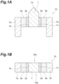
- FIG. 1A is a longitudinal sectional view schematically illustrating an emitter according to a first embodiment
- FIG. 1B is a transverse sectional view of the emitter illustrated in FIG. 1A
- An emitter 10 illustrated in these drawings includes an electron source 1, a pair of heaters 5a and 5b (first and second heaters) generating heat by energization, intermediate members 2a and 2b disposed between the electron source 1 and the heaters 5a and 5b, and a pair of conductive posts 7a and 7b disposed so as to sandwich these configurations.
- the electron source 1 is made of a material (first material) emitting electrons by being heated.
- the intermediate members 2a and 2b are made of a material (second material) lower in thermal conductivity than the material configuring the electron source 1.
- the heaters 5a and 5b are for heating the electron source 1.
- the pair of conductive posts 7a and 7b are for holding the electron source 1 and so on and energizing the heaters 5a and 5b.
- the emitter 10 is provided in, for example, an electron microscope, semiconductor manufacturing equipment, inspection equipment, or processing equipment. Each configuration of the emitter 10 will be described below.
- the electron source 1 is made of the first material (electron emission material) having electron emission properties.
- a tip portion 1a of the electron source 1 is molded in a conical shape, and electrons are emitted from this tip portion 1a.
- the electron source 1 is exposed to each of side surfaces 10a and 10b of the emitter 10.
- the part of the electron source 1 other than the tip portion 1a has a quadrangular prism shape (see FIGS. 1A and 1B ).
- the length of the electron source 1 is, for example, 0.1 to 2 mm, and the length may be 0.2 to 1.5 mm or 0.2 to 1 mm. By the length being 0.1 mm or more, handling tends to be satisfactory. By the length being 2 mm or less, heating tends to be uniform.
- the quadrangular prism part of the electron source 1 has a substantially square sectional shape.
- the length of the side is, for example, 0.02 to 1 mm, and the length may be 0.05 to 0.5 mm or 0.05 to 0.15 mm.
- the material of the electron emission material includes rare earth borides such as lanthanum boride (LaB 6 ) and cerium boride (CeB 6 ); and precious metal-rare earth alloys such as iridium cerium.
- rare earth borides such as lanthanum boride (LaB 6 ) and cerium boride (CeB 6 ); and precious metal-rare earth alloys such as iridium cerium.
- the electron emission material configuring the electron source 1 is preferably a rare earth boride.
- the electron source 1 is preferably a single crystal processed such that the ⁇ 100> orientation of easy electron emission matches the electron emission direction.
- the electron source 1 can be given a desired shape by, for example, electric discharge machining.
- the side surface of the electron source 1 is preferably a (100) crystal plane because the evaporation rate is considered to be slow.
- the material configuring the electron source 1 is higher in thermal conductivity than the material configuring the intermediate members 2a and 2b.
- the thermal conductivity of the material configuring the electron source 1 is preferably 5 W/m ⁇ K or more, more preferably 10 W/m ⁇ K or more.
- the thermal conductivity of this material being 5 W/m ⁇ K or more, the entire electron source 1 tends to be sufficiently uniformly heated by heat from the heaters 5a and 5b.
- the upper limit value of the thermal conductivity of this material is, for example, 200 W/m ⁇ K.
- the thermal conductivities of a plurality of materials are as follows.
- a thermal conductivity value T E of the electron source 1 is preferably sufficiently larger than a thermal conductivity value T I of the intermediate members 2a and 2b.
- the ratio (T E /T I ) of the thermal conductivity value T E of the electron source 1 to the thermal conductivity value T I of the intermediate members 2a and 2b is, for example, 7 to 13, and the ratio may be 8 to 12 or 10 to 11.
- the temperature of the heaters 5a and 5b at a time of energization can be moderately increased.
- the temperature of the heaters 5a and 5b at a time of energization can be made higher than the temperature of the electron source 1 by, for example, approximately 150 to 250°C. As a result, it is possible to suppress deposition of the material configuring the electron source 1 in the vicinity of the heaters 5a and 5b.
- the intermediate members 2a and 2b are disposed so as to be in contact with and cover a pair of surfaces 1b and 1c of the electron source 1 (see FIG. 1B ).
- the intermediate members 2a and 2b are exposed to each of the side surfaces 10a and 10b of the emitter 10.
- the length of the shortest path of the intermediate member passing from the heater to the electron source is 100 ⁇ m or more.
- the thickness of the intermediate member 2a is preferably 100 ⁇ m or more, and the thickness may be 100 to 1000 ⁇ m or 300 to 800 ⁇ m.
- the intermediate members 2a and 2b are made of a material (second material) lower in thermal conductivity than the material configuring the electron source 1.
- the thermal conductivity of the material configuring the intermediate members 2a and 2b is, for example, 100 W/m ⁇ K or less, preferably 1 to 100 W/m ⁇ K and more preferably 1 to 60 W/m ⁇ K.
- the lower limit value of this value may be 2 W/m ⁇ K or 3 W/m ⁇ K.
- the upper limit value of this value may be 45 W/m ⁇ K or 40 W/m ⁇ K.
- the thermal conductivity of this material being 1 W/m ⁇ K or more, heat from the heaters 5a and 5b tends to be sufficiently transmitted to the electron source 1.
- the thermal conductivity of this material being 100 W/m ⁇ K or less, there is a tendency that a sufficient temperature difference can be caused between the heaters 5a and 5b and the electron source 1.
- the material configuring the intermediate members 2a and 2b contains glassy carbon.
- Glassy carbon such as Glassy Carbon (product name, manufactured by Reiho Manufacturing Co., Ltd.) may be used as this material.
- the thermal conductivities of a plurality of materials are as follows.
- the material configuring the intermediate members 2a and 2b is electrically conductive. From the viewpoint of suppressing excessive heat generation of the intermediate members 2a and 2b attributable to energization, it is preferable that the material configuring the intermediate members 2a and 2b is lower in electrical resistivity than the material configuring the heaters 5a and 5b.
- the electrical resistivity of the material configuring the intermediate members 2a and 2b is preferably 300 ⁇ m or less, more preferably 100 ⁇ m or less. By the electrical resistivity of this material being 300 ⁇ m or less, excessive heat generation of the intermediate members 2a and 2b attributable to energization tends to be suppressible. It should be noted that the lower limit value of the electrical resistivity of this material is, for example, 0.1 ⁇ m, and the value may be 0.3 ⁇ m or 1.0 ⁇ m.
- the electrical resistivities of a plurality of materials are as follows.
- the heaters 5a and 5b are made of a high-electrical resistivity material and generate heat by energization.
- the electrical resistivity of the material configuring the heaters 5a and 5b is preferably 500 to 1000 ⁇ m, more preferably 600 to 900 ⁇ m.
- the electrical resistivity of this material being 500 ⁇ m or more, the electron source 1 tends to be sufficiently heatable by energization.
- the electrical resistivity of this material being 1000 ⁇ m or less, sufficient energization tends to be possible.
- Examples of the material configuring the heaters 5a and 5b include pyrolytic graphite and hot-pressed carbon. It should be noted that the electrical resistivity (typical value) of pyrolytic graphite is 800 ⁇ m.
- An electrical resistivity value R H of the heaters 5a and 5b is preferably sufficiently larger than an electrical resistivity value R I of the intermediate members 2a and 2b.
- the ratio (R H /R I ) of the electrical resistivity value R H of the heaters 5a and 5b to the electrical resistivity value R I of the intermediate members 2a and 2b is, for example, 12 to 20, and the ratio may be 13 to 19 or 14 to 18.
- this ratio being 12 or more, the temperature of the heaters 5a and 5b at a time of energization can be sufficiently increased, and deposition of the material configuring the electron source 1 in the vicinity of the heaters 5a and 5b tends to be suppressible.
- this ratio being 20 or less, there is a tendency that the loss of electric power for heating the heaters 5a and 5b can be reduced.
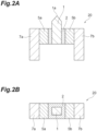
- FIG. 2A is a longitudinal sectional view schematically illustrating an emitter according to a second embodiment
- FIG. 2B is a transverse sectional view of the emitter illustrated in FIG. 2A
- An emitter 20 illustrated in these drawings differs from the emitter 10 according to the first embodiment in that the four side surfaces of the columnar portion of the electron source 1 are covered with an intermediate member 2.
- the intermediate member 2 is interposed between the electron source 1 and the heaters 5a and 5b in the present embodiment
- the intermediate member 2a is interposed between the electron source 1 and the heater 5a
- the intermediate member 2b is interposed between the electron source 1 and the heater 5b in the first embodiment.
- the material of the intermediate member 2 may be the same as the material of the intermediate members 2a and 2b according to the first embodiment.
- FIG. 3A is a longitudinal sectional view schematically illustrating an emitter according to a third embodiment
- FIG. 3B is a transverse sectional view of the emitter illustrated in FIG. 3A
- an intermediate member 3 comprises a columnar portion 3a and a conical part 3b.
- An opening portion 4 is provided in the tip portion of the conical part 3b, and the electron source 1 is inserted in the opening portion 4.
- the surface of the tip of the electron source 1 is an electron emission surface 1f.
- the material of the intermediate member 3 may be the same as the material of the intermediate members 2a and 2b according to the first embodiment.
- the electron source 1 has a quadrangular prism shape (see FIGS. 3A and 3B ).
- the length of the electron source 1 is, for example, 0.1 to 1 mm, and the length may be 0.2 to 0.6 mm or 0.3 mm. By the length being 0.1 mm or more, handling tends to be satisfactory. By the length being 1 mm or less, cracking or the like tends to be less likely to occur.
- the electron source 1 has a substantially square sectional shape.
- the length of the side is, for example, 20 to 300 ⁇ m, and the length may be 50 to 150 ⁇ m or 100 ⁇ m.
- the columnar portion 3a of the intermediate member 3 has a quadrangular prism shape (see FIGS. 3A and 3B ).
- the columnar portion 3a has a substantially square sectional shape.
- the length of the side is, for example, 0.5 to 2 mm, and the length may be 0.6 to 1 mm or 0.7 to 0.9 mm.
- the tip of the electron source 1 may or may not protrude from the tip of the conical part 3b of the intermediate member 3, it is preferable that the tip of the electron source 1 does not protrude from the tip of the conical part 3b of the intermediate member 3.
- unnecessary electron emission that is, lateral electron emission can be sufficiently suppressed.
- the tip portion of the electron source 1 is heated to a high temperature of approximately 1550°C and a high electric field of several kV is applied to the electron source 1.
- the intermediate member 3 By covering the entire side surface of the electron source 1 with the intermediate member 3, there is also the effect of being capable of suppressing the occurrence of a phenomenon called microdischarge.
- microdischarge results from charge accumulation in this whisker to result in electron beam destabilization and device performance decline.
- the intermediate member 3 covers the entire side surface of the electron source 1 without having a cut at a circumferential part. Since the intermediate member 3 is cut-less, lateral electron emission can be sufficiently suppressed.
- the present invention is not limited to the embodiments of the present disclosure described in detail above.
- the sectional shape of the columnar portion may be substantially polygonal instead of being substantially square.
- the shape may be substantially rectangular, substantially rhombic, substantially parallelogrammic, substantially triangular (for example, substantially equilateral-triangular), or substantially regular-hexagonal.
- the sectional shape of the opening portion 4 in the third embodiment may not match the sectional shape of the electron source.
- the shape may be substantially circular, substantially rhombic, substantially parallelogrammic, substantially triangular (for example, substantially equilateral-triangular), or substantially regular-hexagonal.
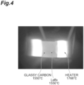
- the temperature of the heater was 1768°C when the emitter was energized under constant current control such that the temperature of the electron source was 1550°C.
- FIG. 4 is a thermographic camera image showing the upper surface temperature of the emitter according to the example. According to the present inventors' examinations, it is preferable from the viewpoint of lanthanum boride deposition prevention that the temperature of the heater is 1700 to 1800°C when the electron source is heated to 1550°C.
- the temperature of the heater was 1634°C when the emitter was energized under constant current control such that the temperature of the electron source was 1550°C.
- an emitter capable of maintaining high reliability even during long-term operation and a device provided with the same.
Landscapes
- Chemical & Material Sciences (AREA)
- Analytical Chemistry (AREA)
- Solid Thermionic Cathode (AREA)
- Electron Sources, Ion Sources (AREA)
Claims (8)
- Emitter (10, 20, 30), umfassend:erste und zweite Heizvorrichtungen (5a, 5b), die durch Erregung Wärme erzeugen;eine Elektronenquelle (1), die ein erstes Material umfasst, das ein Elektron emittiert, indem es von den ersten und zweiten Heizvorrichtungen (5a, 5b) erwärmt wird; undein Zwischenelement (2, 2a, 2b, 3), das zwischen der Elektronenquelle und den ersten und zweiten Heizvorrichtungen (5a, 5b) angeordnet ist, wobei das Zwischenelement (2, 2a, 2b, 3) ein zweites Material mit einer geringeren Wärmeleitfähigkeit als das erste Material umfasst,wobei das erste Material ein Seltenerd-Borid oder eine Edelmetall-Seltenerd-Legierung ist und das zweite Material glasartiger Kohlenstoff ist, undwobei eine Länge eines kürzesten Weges des Zwischenelements (2, 2a, 2b, 3), der von der Heizvorrichtung (5a, 5b) zu der Elektronenquelle (1) führt, 100 µm oder mehr beträgt.
- Emitter (10, 20, 30) nach Anspruch 1, wobeiein elektrischer Widerstandswert des Zwischenelements (2, 2a, 2b, 3) 300 µΩ·m oder weniger beträgt, undein elektrischer Widerstandswert der Heizvorrichtung (5a, 5b) 500 µΩ·m oder mehr beträgt.
- Emitter (10, 20, 30) nach Anspruch 1 oder 2, wobei das erste Material ein Seltenerd-Borid ist.
- Emitter (10, 20, 30) nach Anspruch 3, wobei das erste Material ein Lanthanborid oder ein Ceriumborid ist.
- Emitter (10, 20, 30) nach Anspruch 1 oder 2, wobei das erste Material eine Edelmetall-Seltenerd-Legierung ist.
- Emitter (10, 20, 30) nach Anspruch 5, wobei das erste Material ein Iridium-Cerium ist.
- Emitter nach einem der Ansprüche 1 bis 6, wobei das Zwischenelement (3) eine andere Oberfläche der Elektronenquelle (1) als eine Elektronenemissionsoberfläche (1f) bedeckt.
- Vorrichtung (10, 20, 30), die den Emitter nach einem der Ansprüche 1 bis 7 umfasst.
Applications Claiming Priority (2)
| Application Number | Priority Date | Filing Date | Title |
|---|---|---|---|
| JP2020137423 | 2020-08-17 | ||
| PCT/JP2021/029180 WO2022039042A1 (ja) | 2020-08-17 | 2021-08-05 | エミッター及びこれを備える装置 |
Publications (3)
| Publication Number | Publication Date |
|---|---|
| EP4191636A1 EP4191636A1 (de) | 2023-06-07 |
| EP4191636A4 EP4191636A4 (de) | 2024-01-10 |
| EP4191636B1 true EP4191636B1 (de) | 2025-01-08 |
Family
ID=80322699
Family Applications (1)
| Application Number | Title | Priority Date | Filing Date |
|---|---|---|---|
| EP21858189.0A Active EP4191636B1 (de) | 2020-08-17 | 2021-08-05 | Elektronenemitter |
Country Status (7)
| Country | Link |
|---|---|
| US (1) | US20230298846A1 (de) |
| EP (1) | EP4191636B1 (de) |
| JP (2) | JP7640560B2 (de) |
| KR (1) | KR20230050264A (de) |
| CN (1) | CN115362523B (de) |
| TW (1) | TWI896729B (de) |
| WO (1) | WO2022039042A1 (de) |
Families Citing this family (1)
| Publication number | Priority date | Publication date | Assignee | Title |
|---|---|---|---|---|
| US12586747B2 (en) | 2022-03-29 | 2026-03-24 | Denka Company Limited | Emitter and device comprising same |
Family Cites Families (13)
| Publication number | Priority date | Publication date | Assignee | Title |
|---|---|---|---|---|
| JPS5812695B2 (ja) * | 1977-09-30 | 1983-03-09 | 電気化学工業株式会社 | 熱電子放射陰極の製造法 |
| JPH06231708A (ja) * | 1993-02-04 | 1994-08-19 | Mitsubishi Heavy Ind Ltd | 長尺電子ビーム発生装置 |
| JPH09102562A (ja) * | 1995-10-06 | 1997-04-15 | Kobe Steel Ltd | 高熱伝導性基板及びその製造方法 |
| JP2000164563A (ja) * | 1998-11-26 | 2000-06-16 | Hitachi Ltd | プラズマ処理装置 |
| JP4026513B2 (ja) * | 2003-02-28 | 2007-12-26 | ウシオ電機株式会社 | 放電ランプ |
| JP2006012496A (ja) | 2004-06-23 | 2006-01-12 | Denki Kagaku Kogyo Kk | 電子源 |
| JP4951477B2 (ja) * | 2006-12-04 | 2012-06-13 | 電気化学工業株式会社 | 電子放出源 |
| JP2009295736A (ja) * | 2008-06-04 | 2009-12-17 | Sharp Corp | 発光モジュール |
| JP2011181339A (ja) * | 2010-03-01 | 2011-09-15 | Hiroshi Yasuda | 電子銃およびマルチコラム電子ビーム装置。 |
| JP2017201609A (ja) * | 2016-05-06 | 2017-11-09 | 株式会社Param | 電子銃 |
| JP6938498B2 (ja) * | 2016-07-19 | 2021-09-22 | デンカ株式会社 | 電子源およびその製造方法 |
| JP2019153563A (ja) * | 2018-03-06 | 2019-09-12 | 株式会社Param | 電子銃 |
| WO2021079855A1 (ja) * | 2019-10-21 | 2021-04-29 | 国立研究開発法人物質・材料研究機構 | エミッタ、それを用いた電子銃、それを用いた電子機器、および、その製造方法 |
-
2021
- 2021-08-05 WO PCT/JP2021/029180 patent/WO2022039042A1/ja not_active Ceased
- 2021-08-05 KR KR1020227032102A patent/KR20230050264A/ko not_active Ceased
- 2021-08-05 JP JP2022543366A patent/JP7640560B2/ja active Active
- 2021-08-05 EP EP21858189.0A patent/EP4191636B1/de active Active
- 2021-08-05 US US18/041,408 patent/US20230298846A1/en active Pending
- 2021-08-05 CN CN202180025722.0A patent/CN115362523B/zh active Active
- 2021-08-12 TW TW110129738A patent/TWI896729B/zh active
-
2025
- 2025-02-20 JP JP2025025812A patent/JP2025072670A/ja active Pending
Also Published As
| Publication number | Publication date |
|---|---|
| TWI896729B (zh) | 2025-09-11 |
| TW202213412A (zh) | 2022-04-01 |
| KR20230050264A (ko) | 2023-04-14 |
| JP7640560B2 (ja) | 2025-03-05 |
| JP2025072670A (ja) | 2025-05-09 |
| CN115362523B (zh) | 2025-06-13 |
| EP4191636A1 (de) | 2023-06-07 |
| WO2022039042A1 (ja) | 2022-02-24 |
| CN115362523A (zh) | 2022-11-18 |
| US20230298846A1 (en) | 2023-09-21 |
| EP4191636A4 (de) | 2024-01-10 |
| JPWO2022039042A1 (de) | 2022-02-24 |
Similar Documents
| Publication | Publication Date | Title |
|---|---|---|
| US7364624B2 (en) | Wafer handling apparatus and method of manufacturing thereof | |
| KR20150013497A (ko) | 정전척 및 정전척의 제조 방법 | |
| US8548124B2 (en) | Electron source and cathode cup thereof | |
| US3440475A (en) | Lanthanum hexaboride cathode system for an electron beam generator | |
| US20210242049A1 (en) | Detachable thermal leveler | |
| EP4191636B1 (de) | Elektronenemitter | |
| EP0380205B1 (de) | Schnellheizkathode für Hochleistungsvakuumröhren | |
| US4994706A (en) | Field free, directly heated lanthanum boride cathode | |
| US12586747B2 (en) | Emitter and device comprising same | |
| JP2607251B2 (ja) | 電界放射陰極 | |
| US20220208506A1 (en) | Electron beam emitting assembly | |
| JPH0676730A (ja) | 熱電子放射陰極 | |
| GB2296371A (en) | Cathode arrangements utilizing diamond as an insulator | |
| CN116982135A (zh) | 电子枪阴极支架 | |
| JPH0757617A (ja) | 熱電子発生源 | |
| US4560907A (en) | Ion source | |
| Mattox | Metallizing ceramics using a gas discharge | |
| US20050082960A1 (en) | Internally heated cathode | |
| JP2024062621A (ja) | 電子源及びその製造方法 | |
| JPS61253746A (ja) | ホロ−カソ−ド放電型イオン源 | |
| WO2026052986A1 (en) | Evaporation source, deposition system and method for depositing a material | |
| JPH06231708A (ja) | 長尺電子ビーム発生装置 | |
| JP2006012496A (ja) | 電子源 |
Legal Events
| Date | Code | Title | Description |
|---|---|---|---|
| STAA | Information on the status of an ep patent application or granted ep patent |
Free format text: STATUS: THE INTERNATIONAL PUBLICATION HAS BEEN MADE |
|
| PUAI | Public reference made under article 153(3) epc to a published international application that has entered the european phase |
Free format text: ORIGINAL CODE: 0009012 |
|
| STAA | Information on the status of an ep patent application or granted ep patent |
Free format text: STATUS: REQUEST FOR EXAMINATION WAS MADE |
|
| 17P | Request for examination filed |
Effective date: 20230302 |
|
| AK | Designated contracting states |
Kind code of ref document: A1 Designated state(s): AL AT BE BG CH CY CZ DE DK EE ES FI FR GB GR HR HU IE IS IT LI LT LU LV MC MK MT NL NO PL PT RO RS SE SI SK SM TR |
|
| DAV | Request for validation of the european patent (deleted) | ||
| DAX | Request for extension of the european patent (deleted) | ||
| REG | Reference to a national code |
Ref country code: DE Ref legal event code: R079 Free format text: PREVIOUS MAIN CLASS: H01J0037060000 Ipc: H01J0001240000 Ref document number: 602021024810 Country of ref document: DE |
|
| A4 | Supplementary search report drawn up and despatched |
Effective date: 20231212 |
|
| RIC1 | Information provided on ipc code assigned before grant |
Ipc: H01J 37/065 20060101ALI20231206BHEP Ipc: H01J 1/24 20060101AFI20231206BHEP |
|
| GRAP | Despatch of communication of intention to grant a patent |
Free format text: ORIGINAL CODE: EPIDOSNIGR1 |
|
| STAA | Information on the status of an ep patent application or granted ep patent |
Free format text: STATUS: GRANT OF PATENT IS INTENDED |
|
| RIC1 | Information provided on ipc code assigned before grant |
Ipc: H01J 37/065 20060101ALI20240814BHEP Ipc: H01J 1/24 20060101AFI20240814BHEP |
|
| INTG | Intention to grant announced |
Effective date: 20240917 |
|
| GRAS | Grant fee paid |
Free format text: ORIGINAL CODE: EPIDOSNIGR3 |
|
| GRAA | (expected) grant |
Free format text: ORIGINAL CODE: 0009210 |
|
| STAA | Information on the status of an ep patent application or granted ep patent |
Free format text: STATUS: THE PATENT HAS BEEN GRANTED |
|
| AK | Designated contracting states |
Kind code of ref document: B1 Designated state(s): AL AT BE BG CH CY CZ DE DK EE ES FI FR GB GR HR HU IE IS IT LI LT LU LV MC MK MT NL NO PL PT RO RS SE SI SK SM TR |
|
| P01 | Opt-out of the competence of the unified patent court (upc) registered |
Free format text: CASE NUMBER: APP_63255/2024 Effective date: 20241128 |
|
| REG | Reference to a national code |
Ref country code: GB Ref legal event code: FG4D |
|
| REG | Reference to a national code |
Ref country code: CH Ref legal event code: EP |
|
| REG | Reference to a national code |
Ref country code: DE Ref legal event code: R096 Ref document number: 602021024810 Country of ref document: DE |
|
| REG | Reference to a national code |
Ref country code: IE Ref legal event code: FG4D |
|
| REG | Reference to a national code |
Ref country code: SE Ref legal event code: TRGR |
|
| REG | Reference to a national code |
Ref country code: LT Ref legal event code: MG9D |
|
| REG | Reference to a national code |
Ref country code: NL Ref legal event code: MP Effective date: 20250108 |
|
| PG25 | Lapsed in a contracting state [announced via postgrant information from national office to epo] |
Ref country code: NL Free format text: LAPSE BECAUSE OF FAILURE TO SUBMIT A TRANSLATION OF THE DESCRIPTION OR TO PAY THE FEE WITHIN THE PRESCRIBED TIME-LIMIT Effective date: 20250108 |
|
| PG25 | Lapsed in a contracting state [announced via postgrant information from national office to epo] |
Ref country code: RS Free format text: LAPSE BECAUSE OF FAILURE TO SUBMIT A TRANSLATION OF THE DESCRIPTION OR TO PAY THE FEE WITHIN THE PRESCRIBED TIME-LIMIT Effective date: 20250408 |
|
| PG25 | Lapsed in a contracting state [announced via postgrant information from national office to epo] |
Ref country code: FI Free format text: LAPSE BECAUSE OF FAILURE TO SUBMIT A TRANSLATION OF THE DESCRIPTION OR TO PAY THE FEE WITHIN THE PRESCRIBED TIME-LIMIT Effective date: 20250108 |
|
| PG25 | Lapsed in a contracting state [announced via postgrant information from national office to epo] |
Ref country code: PL Free format text: LAPSE BECAUSE OF FAILURE TO SUBMIT A TRANSLATION OF THE DESCRIPTION OR TO PAY THE FEE WITHIN THE PRESCRIBED TIME-LIMIT Effective date: 20250108 |
|
| PG25 | Lapsed in a contracting state [announced via postgrant information from national office to epo] |
Ref country code: ES Free format text: LAPSE BECAUSE OF FAILURE TO SUBMIT A TRANSLATION OF THE DESCRIPTION OR TO PAY THE FEE WITHIN THE PRESCRIBED TIME-LIMIT Effective date: 20250108 |
|
| PG25 | Lapsed in a contracting state [announced via postgrant information from national office to epo] |
Ref country code: NO Free format text: LAPSE BECAUSE OF FAILURE TO SUBMIT A TRANSLATION OF THE DESCRIPTION OR TO PAY THE FEE WITHIN THE PRESCRIBED TIME-LIMIT Effective date: 20250408 Ref country code: IS Free format text: LAPSE BECAUSE OF FAILURE TO SUBMIT A TRANSLATION OF THE DESCRIPTION OR TO PAY THE FEE WITHIN THE PRESCRIBED TIME-LIMIT Effective date: 20250508 |
|
| PG25 | Lapsed in a contracting state [announced via postgrant information from national office to epo] |
Ref country code: HR Free format text: LAPSE BECAUSE OF FAILURE TO SUBMIT A TRANSLATION OF THE DESCRIPTION OR TO PAY THE FEE WITHIN THE PRESCRIBED TIME-LIMIT Effective date: 20250108 |
|
| PG25 | Lapsed in a contracting state [announced via postgrant information from national office to epo] |
Ref country code: PT Free format text: LAPSE BECAUSE OF FAILURE TO SUBMIT A TRANSLATION OF THE DESCRIPTION OR TO PAY THE FEE WITHIN THE PRESCRIBED TIME-LIMIT Effective date: 20250508 Ref country code: LV Free format text: LAPSE BECAUSE OF FAILURE TO SUBMIT A TRANSLATION OF THE DESCRIPTION OR TO PAY THE FEE WITHIN THE PRESCRIBED TIME-LIMIT Effective date: 20250108 |
|
| PG25 | Lapsed in a contracting state [announced via postgrant information from national office to epo] |
Ref country code: BG Free format text: LAPSE BECAUSE OF FAILURE TO SUBMIT A TRANSLATION OF THE DESCRIPTION OR TO PAY THE FEE WITHIN THE PRESCRIBED TIME-LIMIT Effective date: 20250108 Ref country code: GR Free format text: LAPSE BECAUSE OF FAILURE TO SUBMIT A TRANSLATION OF THE DESCRIPTION OR TO PAY THE FEE WITHIN THE PRESCRIBED TIME-LIMIT Effective date: 20250409 |
|
| PG25 | Lapsed in a contracting state [announced via postgrant information from national office to epo] |
Ref country code: SM Free format text: LAPSE BECAUSE OF FAILURE TO SUBMIT A TRANSLATION OF THE DESCRIPTION OR TO PAY THE FEE WITHIN THE PRESCRIBED TIME-LIMIT Effective date: 20250108 |
|
| REG | Reference to a national code |
Ref country code: DE Ref legal event code: R097 Ref document number: 602021024810 Country of ref document: DE |
|
| PG25 | Lapsed in a contracting state [announced via postgrant information from national office to epo] |
Ref country code: DK Free format text: LAPSE BECAUSE OF FAILURE TO SUBMIT A TRANSLATION OF THE DESCRIPTION OR TO PAY THE FEE WITHIN THE PRESCRIBED TIME-LIMIT Effective date: 20250108 |
|
| PGFP | Annual fee paid to national office [announced via postgrant information from national office to epo] |
Ref country code: DE Payment date: 20250702 Year of fee payment: 5 |
|
| PGFP | Annual fee paid to national office [announced via postgrant information from national office to epo] |
Ref country code: AT Payment date: 20251020 Year of fee payment: 5 |
|
| PGFP | Annual fee paid to national office [announced via postgrant information from national office to epo] |
Ref country code: SE Payment date: 20250702 Year of fee payment: 5 |
|
| PG25 | Lapsed in a contracting state [announced via postgrant information from national office to epo] |
Ref country code: CZ Free format text: LAPSE BECAUSE OF FAILURE TO SUBMIT A TRANSLATION OF THE DESCRIPTION OR TO PAY THE FEE WITHIN THE PRESCRIBED TIME-LIMIT Effective date: 20250108 Ref country code: EE Free format text: LAPSE BECAUSE OF FAILURE TO SUBMIT A TRANSLATION OF THE DESCRIPTION OR TO PAY THE FEE WITHIN THE PRESCRIBED TIME-LIMIT Effective date: 20250108 |
|
| PG25 | Lapsed in a contracting state [announced via postgrant information from national office to epo] |
Ref country code: RO Free format text: LAPSE BECAUSE OF FAILURE TO SUBMIT A TRANSLATION OF THE DESCRIPTION OR TO PAY THE FEE WITHIN THE PRESCRIBED TIME-LIMIT Effective date: 20250108 |
|
| PG25 | Lapsed in a contracting state [announced via postgrant information from national office to epo] |
Ref country code: SK Free format text: LAPSE BECAUSE OF FAILURE TO SUBMIT A TRANSLATION OF THE DESCRIPTION OR TO PAY THE FEE WITHIN THE PRESCRIBED TIME-LIMIT Effective date: 20250108 |
|
| PLBE | No opposition filed within time limit |
Free format text: ORIGINAL CODE: 0009261 |
|
| STAA | Information on the status of an ep patent application or granted ep patent |
Free format text: STATUS: NO OPPOSITION FILED WITHIN TIME LIMIT |
|
| REG | Reference to a national code |
Ref country code: CH Ref legal event code: L10 Free format text: ST27 STATUS EVENT CODE: U-0-0-L10-L00 (AS PROVIDED BY THE NATIONAL OFFICE) Effective date: 20251119 |
|
| 26N | No opposition filed |
Effective date: 20251009 |
|
| PG25 | Lapsed in a contracting state [announced via postgrant information from national office to epo] |
Ref country code: IT Free format text: LAPSE BECAUSE OF FAILURE TO SUBMIT A TRANSLATION OF THE DESCRIPTION OR TO PAY THE FEE WITHIN THE PRESCRIBED TIME-LIMIT Effective date: 20250108 |
|
| REG | Reference to a national code |
Ref country code: CH Ref legal event code: H13 Free format text: ST27 STATUS EVENT CODE: U-0-0-H10-H13 (AS PROVIDED BY THE NATIONAL OFFICE) Effective date: 20260324 |
|
| PG25 | Lapsed in a contracting state [announced via postgrant information from national office to epo] |
Ref country code: MC Free format text: LAPSE BECAUSE OF FAILURE TO SUBMIT A TRANSLATION OF THE DESCRIPTION OR TO PAY THE FEE WITHIN THE PRESCRIBED TIME-LIMIT Effective date: 20250108 |
|
| PG25 | Lapsed in a contracting state [announced via postgrant information from national office to epo] |
Ref country code: LU Free format text: LAPSE BECAUSE OF NON-PAYMENT OF DUE FEES Effective date: 20250805 |