EP4156871A1 - Circuit board - Google Patents
Circuit board Download PDFInfo
- Publication number
- EP4156871A1 EP4156871A1 EP21808883.9A EP21808883A EP4156871A1 EP 4156871 A1 EP4156871 A1 EP 4156871A1 EP 21808883 A EP21808883 A EP 21808883A EP 4156871 A1 EP4156871 A1 EP 4156871A1
- Authority
- EP
- European Patent Office
- Prior art keywords
- layer
- circuit pattern
- disposed
- insulating layer
- gold
- Prior art date
- Legal status (The legal status is an assumption and is not a legal conclusion. Google has not performed a legal analysis and makes no representation as to the accuracy of the status listed.)
- Pending
Links
- 239000010931 gold Substances 0.000 claims abstract description 121
- 230000004888 barrier function Effects 0.000 claims abstract description 118
- KDLHZDBZIXYQEI-UHFFFAOYSA-N Palladium Chemical compound [Pd] KDLHZDBZIXYQEI-UHFFFAOYSA-N 0.000 claims abstract description 109
- PCHJSUWPFVWCPO-UHFFFAOYSA-N gold Chemical compound [Au] PCHJSUWPFVWCPO-UHFFFAOYSA-N 0.000 claims abstract description 67
- 229910052737 gold Inorganic materials 0.000 claims abstract description 67
- 229910052763 palladium Inorganic materials 0.000 claims abstract description 42
- 229910000679 solder Inorganic materials 0.000 claims abstract description 28
- 239000010410 layer Substances 0.000 description 442
- 229910052751 metal Inorganic materials 0.000 description 137
- 239000002184 metal Substances 0.000 description 137
- 239000011241 protective layer Substances 0.000 description 43
- RYGMFSIKBFXOCR-UHFFFAOYSA-N Copper Chemical compound [Cu] RYGMFSIKBFXOCR-UHFFFAOYSA-N 0.000 description 19
- 239000010949 copper Substances 0.000 description 17
- 239000007769 metal material Substances 0.000 description 17
- 238000000034 method Methods 0.000 description 17
- 229910052802 copper Inorganic materials 0.000 description 16
- 230000008569 process Effects 0.000 description 13
- 239000000758 substrate Substances 0.000 description 13
- 238000013508 migration Methods 0.000 description 12
- 230000005012 migration Effects 0.000 description 12
- JPVYNHNXODAKFH-UHFFFAOYSA-N Cu2+ Chemical compound [Cu+2] JPVYNHNXODAKFH-UHFFFAOYSA-N 0.000 description 10
- 229910001431 copper ion Inorganic materials 0.000 description 10
- 238000004519 manufacturing process Methods 0.000 description 10
- 238000007747 plating Methods 0.000 description 10
- DNIAPMSPPWPWGF-UHFFFAOYSA-N Propylene glycol Chemical compound CC(O)CO DNIAPMSPPWPWGF-UHFFFAOYSA-N 0.000 description 6
- 238000004891 communication Methods 0.000 description 5
- 230000010354 integration Effects 0.000 description 5
- 230000000149 penetrating effect Effects 0.000 description 5
- 229920000089 Cyclic olefin copolymer Polymers 0.000 description 4
- 239000011889 copper foil Substances 0.000 description 3
- 230000000694 effects Effects 0.000 description 3
- 238000005516 engineering process Methods 0.000 description 3
- 238000012986 modification Methods 0.000 description 3
- 230000004048 modification Effects 0.000 description 3
- 239000004713 Cyclic olefin copolymer Substances 0.000 description 2
- 239000004642 Polyimide Substances 0.000 description 2
- BQCADISMDOOEFD-UHFFFAOYSA-N Silver Chemical compound [Ag] BQCADISMDOOEFD-UHFFFAOYSA-N 0.000 description 2
- 239000000654 additive Substances 0.000 description 2
- 238000013461 design Methods 0.000 description 2
- 238000005530 etching Methods 0.000 description 2
- 239000011810 insulating material Substances 0.000 description 2
- 229920003229 poly(methyl methacrylate) Polymers 0.000 description 2
- 239000004417 polycarbonate Substances 0.000 description 2
- 229920000515 polycarbonate Polymers 0.000 description 2
- -1 polyethylene terephthalate Polymers 0.000 description 2
- 229920000139 polyethylene terephthalate Polymers 0.000 description 2
- 239000005020 polyethylene terephthalate Substances 0.000 description 2
- 229920001721 polyimide Polymers 0.000 description 2
- 239000004926 polymethyl methacrylate Substances 0.000 description 2
- 239000004065 semiconductor Substances 0.000 description 2
- 229910052709 silver Inorganic materials 0.000 description 2
- 239000004332 silver Substances 0.000 description 2
- 239000000126 substance Substances 0.000 description 2
- 239000005354 aluminosilicate glass Substances 0.000 description 1
- 230000005540 biological transmission Effects 0.000 description 1
- 230000000052 comparative effect Effects 0.000 description 1
- 239000004020 conductor Substances 0.000 description 1
- 238000009429 electrical wiring Methods 0.000 description 1
- 238000011156 evaluation Methods 0.000 description 1
- 229920002457 flexible plastic Polymers 0.000 description 1
- 239000011521 glass Substances 0.000 description 1
- AMGQUBHHOARCQH-UHFFFAOYSA-N indium;oxotin Chemical compound [In].[Sn]=O AMGQUBHHOARCQH-UHFFFAOYSA-N 0.000 description 1
- 239000000463 material Substances 0.000 description 1
- 238000002161 passivation Methods 0.000 description 1
- 239000004033 plastic Substances 0.000 description 1
- 229920003023 plastic Polymers 0.000 description 1
- 229910052594 sapphire Inorganic materials 0.000 description 1
- 239000010980 sapphire Substances 0.000 description 1
- 239000005361 soda-lime glass Substances 0.000 description 1
- 239000005341 toughened glass Substances 0.000 description 1
- 238000012546 transfer Methods 0.000 description 1
- 239000013585 weight reducing agent Substances 0.000 description 1
Images


Classifications
-
- H—ELECTRICITY
- H05—ELECTRIC TECHNIQUES NOT OTHERWISE PROVIDED FOR
- H05K—PRINTED CIRCUITS; CASINGS OR CONSTRUCTIONAL DETAILS OF ELECTRIC APPARATUS; MANUFACTURE OF ASSEMBLAGES OF ELECTRICAL COMPONENTS
- H05K1/00—Printed circuits
- H05K1/02—Details
- H05K1/0213—Electrical arrangements not otherwise provided for
- H05K1/0254—High voltage adaptations; Electrical insulation details; Overvoltage or electrostatic discharge protection ; Arrangements for regulating voltages or for using plural voltages
- H05K1/0256—Electrical insulation details, e.g. around high voltage areas
-
- H—ELECTRICITY
- H05—ELECTRIC TECHNIQUES NOT OTHERWISE PROVIDED FOR
- H05K—PRINTED CIRCUITS; CASINGS OR CONSTRUCTIONAL DETAILS OF ELECTRIC APPARATUS; MANUFACTURE OF ASSEMBLAGES OF ELECTRICAL COMPONENTS
- H05K1/00—Printed circuits
- H05K1/02—Details
- H05K1/09—Use of materials for the conductive, e.g. metallic pattern
-
- H—ELECTRICITY
- H05—ELECTRIC TECHNIQUES NOT OTHERWISE PROVIDED FOR
- H05K—PRINTED CIRCUITS; CASINGS OR CONSTRUCTIONAL DETAILS OF ELECTRIC APPARATUS; MANUFACTURE OF ASSEMBLAGES OF ELECTRICAL COMPONENTS
- H05K3/00—Apparatus or processes for manufacturing printed circuits
- H05K3/10—Apparatus or processes for manufacturing printed circuits in which conductive material is applied to the insulating support in such a manner as to form the desired conductive pattern
- H05K3/18—Apparatus or processes for manufacturing printed circuits in which conductive material is applied to the insulating support in such a manner as to form the desired conductive pattern using precipitation techniques to apply the conductive material
- H05K3/181—Apparatus or processes for manufacturing printed circuits in which conductive material is applied to the insulating support in such a manner as to form the desired conductive pattern using precipitation techniques to apply the conductive material by electroless plating
- H05K3/182—Apparatus or processes for manufacturing printed circuits in which conductive material is applied to the insulating support in such a manner as to form the desired conductive pattern using precipitation techniques to apply the conductive material by electroless plating characterised by the patterning method
- H05K3/184—Apparatus or processes for manufacturing printed circuits in which conductive material is applied to the insulating support in such a manner as to form the desired conductive pattern using precipitation techniques to apply the conductive material by electroless plating characterised by the patterning method using masks
-
- H—ELECTRICITY
- H05—ELECTRIC TECHNIQUES NOT OTHERWISE PROVIDED FOR
- H05K—PRINTED CIRCUITS; CASINGS OR CONSTRUCTIONAL DETAILS OF ELECTRIC APPARATUS; MANUFACTURE OF ASSEMBLAGES OF ELECTRICAL COMPONENTS
- H05K3/00—Apparatus or processes for manufacturing printed circuits
- H05K3/22—Secondary treatment of printed circuits
- H05K3/24—Reinforcing the conductive pattern
- H05K3/244—Finish plating of conductors, especially of copper conductors, e.g. for pads or lands
-
- H—ELECTRICITY
- H05—ELECTRIC TECHNIQUES NOT OTHERWISE PROVIDED FOR
- H05K—PRINTED CIRCUITS; CASINGS OR CONSTRUCTIONAL DETAILS OF ELECTRIC APPARATUS; MANUFACTURE OF ASSEMBLAGES OF ELECTRICAL COMPONENTS
- H05K3/00—Apparatus or processes for manufacturing printed circuits
- H05K3/22—Secondary treatment of printed circuits
- H05K3/28—Applying non-metallic protective coatings
- H05K3/282—Applying non-metallic protective coatings for inhibiting the corrosion of the circuit, e.g. for preserving the solderability
-
- H—ELECTRICITY
- H05—ELECTRIC TECHNIQUES NOT OTHERWISE PROVIDED FOR
- H05K—PRINTED CIRCUITS; CASINGS OR CONSTRUCTIONAL DETAILS OF ELECTRIC APPARATUS; MANUFACTURE OF ASSEMBLAGES OF ELECTRICAL COMPONENTS
- H05K2201/00—Indexing scheme relating to printed circuits covered by H05K1/00
- H05K2201/03—Conductive materials
- H05K2201/0332—Structure of the conductor
- H05K2201/0335—Layered conductors or foils
- H05K2201/0338—Layered conductor, e.g. layered metal substrate, layered finish layer or layered thin film adhesion layer
-
- H—ELECTRICITY
- H05—ELECTRIC TECHNIQUES NOT OTHERWISE PROVIDED FOR
- H05K—PRINTED CIRCUITS; CASINGS OR CONSTRUCTIONAL DETAILS OF ELECTRIC APPARATUS; MANUFACTURE OF ASSEMBLAGES OF ELECTRICAL COMPONENTS
- H05K2201/00—Indexing scheme relating to printed circuits covered by H05K1/00
- H05K2201/03—Conductive materials
- H05K2201/0332—Structure of the conductor
- H05K2201/0335—Layered conductors or foils
- H05K2201/0341—Intermediate metal, e.g. before reinforcing of conductors by plating
-
- H—ELECTRICITY
- H05—ELECTRIC TECHNIQUES NOT OTHERWISE PROVIDED FOR
- H05K—PRINTED CIRCUITS; CASINGS OR CONSTRUCTIONAL DETAILS OF ELECTRIC APPARATUS; MANUFACTURE OF ASSEMBLAGES OF ELECTRICAL COMPONENTS
- H05K2201/00—Indexing scheme relating to printed circuits covered by H05K1/00
- H05K2201/03—Conductive materials
- H05K2201/0332—Structure of the conductor
- H05K2201/0335—Layered conductors or foils
- H05K2201/0361—Etched tri-metal structure, i.e. metal layers or metal patterns on both sides of a different central metal layer which is later at least partly etched
-
- H—ELECTRICITY
- H05—ELECTRIC TECHNIQUES NOT OTHERWISE PROVIDED FOR
- H05K—PRINTED CIRCUITS; CASINGS OR CONSTRUCTIONAL DETAILS OF ELECTRIC APPARATUS; MANUFACTURE OF ASSEMBLAGES OF ELECTRICAL COMPONENTS
- H05K2203/00—Indexing scheme relating to apparatus or processes for manufacturing printed circuits covered by H05K3/00
- H05K2203/05—Patterning and lithography; Masks; Details of resist
- H05K2203/0562—Details of resist
- H05K2203/0597—Resist applied over the edges or sides of conductors, e.g. for protection during etching or plating
-
- H—ELECTRICITY
- H05—ELECTRIC TECHNIQUES NOT OTHERWISE PROVIDED FOR
- H05K—PRINTED CIRCUITS; CASINGS OR CONSTRUCTIONAL DETAILS OF ELECTRIC APPARATUS; MANUFACTURE OF ASSEMBLAGES OF ELECTRICAL COMPONENTS
- H05K3/00—Apparatus or processes for manufacturing printed circuits
- H05K3/007—Manufacture or processing of a substrate for a printed circuit board supported by a temporary or sacrificial carrier
-
- H—ELECTRICITY
- H05—ELECTRIC TECHNIQUES NOT OTHERWISE PROVIDED FOR
- H05K—PRINTED CIRCUITS; CASINGS OR CONSTRUCTIONAL DETAILS OF ELECTRIC APPARATUS; MANUFACTURE OF ASSEMBLAGES OF ELECTRICAL COMPONENTS
- H05K3/00—Apparatus or processes for manufacturing printed circuits
- H05K3/02—Apparatus or processes for manufacturing printed circuits in which the conductive material is applied to the surface of the insulating support and is thereafter removed from such areas of the surface which are not intended for current conducting or shielding
-
- H—ELECTRICITY
- H05—ELECTRIC TECHNIQUES NOT OTHERWISE PROVIDED FOR
- H05K—PRINTED CIRCUITS; CASINGS OR CONSTRUCTIONAL DETAILS OF ELECTRIC APPARATUS; MANUFACTURE OF ASSEMBLAGES OF ELECTRICAL COMPONENTS
- H05K3/00—Apparatus or processes for manufacturing printed circuits
- H05K3/22—Secondary treatment of printed circuits
- H05K3/28—Applying non-metallic protective coatings
Definitions
- An embodiment relates to a circuit board.
- a line width of a circuit has been miniaturized as miniaturization, weight reduction, and integration of an electronic component are accelerated.
- a circuit line width of a package substrate or a printed circuit board on which the semiconductor chip is mounted has been miniaturized to several micrometers or less.
- an embedded trace substrate (hereinafter referred to as "ETS") method for embedding a copper foil in an insulating layer in order to implement a fine circuit pattern has been used in the industry.
- ETS embedded trace substrate
- the copper foil circuit is manufactured in an embedded form in the insulating layer, and thus there is no circuit loss due to etching and it is advantageous for miniaturizing the circuit pitch.
- the 5G communication system uses ultra-high frequency (mmWave) bands (sub 6GHz, 28GHz, 38GHz, or higher frequencies) to achieve high data transfer rates.
- mmWave ultra-high frequency bands
- integration technologies such as beamforming, massive multi-input multi-output (massive MIMO), and array antennas have been developed in the 5G communication system in order to reduce a path loss of radio waves and increase a transmission distance of radio waves in the ultra-high frequency band.
- Antenna systems are relatively large given that they can consist of hundreds of active antennas of wavelengths in these frequency bands.
- an antenna and AP module are patterned or mounted on the printed circuit board, low loss on the printed circuit board is very important. This means that several substrates constituting the active antenna system, that is, an antenna substrate, an antenna power feeding substrate, a transceiver substrate, and a baseband substrate, should be integrated into one compact unit.
- the circuit board applied to the 5G communication system as described above is manufactured according to a trend of light, thin and compact, and accordingly, the circuit pattern is gradually becoming finer.
- an interval between the patterns in a circuit board including a conventional fine circuit pattern becomes narrower as the pitch between the patterns becomes smaller, and thus, reliability problems occur. Specifically, migration of a metal material constituting a circuit pattern in a conventional circuit board occurs during reliability evaluation, thereby causing a reliability problem.
- the embodiment provides a circuit board having a novel structure and a method of manufacturing the same.
- the embodiment provides a circuit board capable of suppressing migration of a metal material constituting a circuit pattern to an insulating layer and a method of manufacturing the same.
- the embodiment provides a circuit board capable of suppressing migration of a metal material constituting a circuit pattern to a solder resist and a method of manufacturing the same.
- a circuit board includes an insulating layer; a first circuit pattern disposed on a first surface of the insulating layer; a first solder resist disposed on the first surface of the insulating layer; and a first barrier layer including a first-first portion disposed between the first solder resist and the first circuit pattern, and a first-second portion disposed between the insulating layer and the first circuit pattern; wherein the firs-first portion of the first barrier layer includes: a first-first gold (Au) layer disposed under a lower surface of the first circuit pattern; and a first-first palladium (Pd) layer disposed under a lower surface of the first-first gold (Au) layer; wherein the first-second portion of the first barrier layer includes: a first-second gold (Au) layer disposed to surround a side surface and an upper surface of the first circuit pattern; and a first-second palladium (Pd) layer disposed to surround the first-second gold (Au) layer; and wherein the first circuit pattern is not in
- the first-first gold (Au) layer has a first width
- a lower surface of the first circuit pattern has a second width smaller than the first width
- the lower surface of the first-first gold (Au) layer includes: a first region in contact with a lower surface of the first circuit pattern; a second region in contact with the first-second palladium (Pd) layer; and a third region in contact with the first-second gold (Au) layer.
- the first circuit pattern is buried in a lower region of the insulating layer.
- the lower surface of the first circuit pattern is positioned on the same plane as a lower surface of the insulating layer, and the first-first portion of the first barrier layer is disposed to protrude downward from the lower surface of the insulating layer.
- the circuit board further includes a second circuit pattern disposed on a second surface of the insulating layer; a second solder resist disposed on the second surface of the insulating layer; and a second barrier layer including a second-first portion disposed between the insulating layer and the second circuit pattern and a second-second portion disposed between the second solder resist and the second circuit pattern.
- the second-first portion of the second barrier layer includes: a second-first gold (Au) layer disposed under a lower surface of the second circuit pattern; and a second-first palladium (Pd) layer disposed between a lower surface of the second-first gold (Au) layer and an upper surface of the insulating layer; wherein the second-second portion of the second barrier layer includes: a second-second gold (Au) layer disposed to surround a side surface and an upper surface of the second circuit pattern; and a second-second palladium (Pd) layer disposed to surround the second-second gold (Au) layer; and wherein the second circuit pattern is not in contact with the insulating layer and the second solder resist by the second-first portion and the second-second portion of the second barrier layer.
- a second-first gold (Au) layer disposed under a lower surface of the second circuit pattern
- a second-first palladium (Pd) layer disposed between a lower surface of the second-first gold (Au) layer and an upper surface
- the second-first gold (Au) layer has a first width, and wherein a lower surface of the second circuit pattern has a second width smaller than the first width.
- a lower surface of the second-first gold (Au) layer includes: a first region in contact with a lower surface of the second circuit pattern; a second region in contact with the second-second palladium (Pd) layer; and a third region in contact with the second-second gold (Au) layer.
- the second circuit pattern is disposed to protrude on the upper surface of the insulating layer.
- a manufacturing method of a circuit board includes: preparing a carrier board; forming a first-first portion of a first barrier layer on the carrier board; forming a first circuit pattern on the first-first portion of the first barrier layer; forming a first-second portion of the first barrier layer on the first circuit pattern; forming an insulating layer covering the first circuit pattern on the first-first portion of the first barrier layer; forming a second-first portion of a second barrier layer on the insulating layer; forming a second circuit pattern on the second-first portion of the second barrier layer; forming a second-second portion of the second barrier layer on the second circuit pattern; removing the carrier board; forming a first solder resist under a lower surface of the insulating layer; and forming a second solder resist on an upper surface of the insulating layer, wherein the firs-first portion of the first barrier layer includes: a first-first gold (Au) layer disposed under a lower surface of the first circuit pattern; and
- first circuit pattern is not in contact with the first solder resist and the insulating layer by the first-first portion and the first-second portion of the first barrier layer
- second circuit pattern is not in contact with the insulating layer and the second solder resist by the second-first portion and the second-second portion of the second barrier layer.
- first-first gold (Au) layer or the second-first gold (Au) layer has a first width
- a lower surface of the first circuit pattern or a lower surface of the second circuit pattern has a second width smaller than the first width
- a lower surface of the first-first gold (Au) layer includes a first region in contact with a lower surface of the first circuit pattern, a second region in contact with the first-second palladium (Pd) layer, and a third region in contact with the first-second gold (Au) layer.
- a lower surface of the first circuit pattern is positioned on the same plane as a lower surface of the insulating layer, and the first-first portion of the first barrier layer is disposed to protrude downward from the lower surface of the insulating layer.
- the embodiment provides a circuit board including an insulating layer and a circuit pattern.
- the circuit pattern includes a metal material.
- the circuit pattern including the metal material does not directly contact the insulating layer.
- a barrier layer is disposed around the circuit pattern. Accordingly, the embodiment may prevent the metal material constituting the circuit pattern from penetrating into the insulating layer, thereby improving electrical and/or physical reliability of the circuit board.
- the barrier layer when the circuit pattern includes copper, the barrier layer includes a gold metal layer disposed around the circuit pattern and containing gold (Au), and a palladium metal layer disposed around the gold metal layer and including palladium (Pd).
- the palladium metal layer may prevent copper constituting the circuit pattern from penetrating toward the insulating layer, and accordingly, it is possible to improve reliability by suppressing the occurrence of copper migration.
- the gold metal layer is disposed between the palladium metal layer and the circuit pattern to form the palladium metal layer. In this case, the gold metal layer includes gold (Au) having a larger grain size than other layers, and thus the palladium metal layer can be stably formed.
- the ITO Indium Tin Oxide
- the barrier layer may prevent silver (Ag) constituting the circuit pattern from penetrating into the insulating layer.
- the barrier layer in the embodiment is also formed on a circuit pattern disposed on an outermost layer among the circuit patterns. This may prevent migration of copper constituting the circuit pattern of the outermost layer to a solder resist.
- a portion of the barrier layer is disposed on a surface of a buried pattern in the ETS (Embedded Trace Substrate) structure of the embodiment.
- the barrier layer is disposed to protrude on the surface of the buried pattern, and this may function as a mounting pad on which a solder layer for mounting a device is disposed. That is, a buried pattern of a conventional ETS structure is formed in a fine pattern, as a result, it was not possible to function as a mounting pad only with a simple pattern, and accordingly, a separate mounting pad having a structure that is buried in the insulating layer or protrudes above the surface of the insulating layer has to be formed.
- the embodiment allows a portion of the barrier layer to have a structure protruding on a surface of the insulating layer, and accordingly, the barrier layer can be used as a mounting pad, thereby simplifying the manufacturing process.
- the singular forms may also include the plural forms unless specifically stated in the phrase, and may include at least one of all combinations that may be combined in A, B, and C when described in "at least one (or more) of A (and), B, and C". Further, in describing the elements of the embodiments of the present invention, the terms such as first, second, A, B, (a), and (b) may be used.
- the "on (over)” or “under (below)” may include not only when two elements are directly connected to each other, but also when one or more other elements are formed or disposed between two elements. Further, when expressed as “on (over)” or “under (below)", it may include not only the upper direction but also the lower direction based on one element.
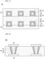
- FIG. 1 is a view showing a circuit board according to an embodiment.
- the circuit board Before describing of the present invention, recently, 5G technology has been developed, and accordingly, interest in circuit boards that can reflect it is increasing. At this time, the circuit board must have a high multi-layer structure in order to apply the 5G technology, and accordingly the circuit pattern must be miniaturized.
- a comparative example makes it possible to form a fine pattern, there is a problem in that it cannot be stably protected.
- a circuit pattern applied to a circuit board for 5G has a narrow line width, and accordingly, an interval between the patterns is narrowed.
- the prior art can form a fine pattern, it cannot be suppressed when migration of a metal material constituting the fine pattern occurs, and thus there is a reliability problem. Accordingly, the embodiment provides a circuit board having a new structure that can solve the reliability problem.
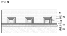
- the circuit board includes an insulating layer 140, a first circuit pattern 130, a first barrier layer 120 and 130, a second circuit pattern 160, and a second barrier layer 150 and 170, a first protective layer 180, and a second protective layer 185.
- a circuit board according to an embodiment may have a multilayer structure based on an insulating layer. That is, although the circuit board in FIG. 1 is illustrated as including a single insulating layer, the embodiment is not limited thereto.
- the circuit board in the embodiment may include a plurality of insulating layers.
- the insulating layer 140 of FIG. 1 may represent a first outermost insulating layer among a plurality of insulating layers, and the first circuit pattern 130 may represent a first outer layer circuit pattern protruding on the first outermost insulating layer.
- the insulating layer 140 of FIG. 1 may represent a second outermost insulating layer among a plurality of insulating layers, and the second circuit pattern 160 may represent a second outer layer circuit pattern buried in the second outermost insulating layer.
- the insulating layer 140 may represent any one specific layer in a plurality of stacked structures.
- the insulating layer 140 is a substrate on which an electric circuit capable of changing wiring is formed, and may include a printed circuit board, a wiring board, and an insulating substrate made of an insulating material capable of forming circuit patterns on a surface.
- the insulating layer 140 may be rigid or flexible.
- the insulating layer 140 may include glass or plastic.
- the insulating layer 140 may include a chemically tempered/semi-tempered glass, such as soda lime glass, aluminosilicate glass, etc., a tempered or flexible plastic such as polyimide (PI), polyethylene terephthalate (PET), propylene glycol (PPG), polycarbonate (PC), etc., or sapphire.
- PI polyimide
- PET polyethylene terephthalate
- PPG propylene glycol
- PC polycarbonate
- the insulating layer 140 may include an optically isotropic film.
- the insulating layer 140 may include cyclic olefin copolymer (COC), cyclic olefin polymer (COP), optically isotropic PC, optically isotropic polymethylmethacrylate (PMMA), or the like.
- the insulating layer 140 may be partially bent while having a curved surface. That is, the insulating layer 140 may partially have a plane and may partially be bent while having a curved surface. Specifically, an end portion of the insulating layer 140 may be bent while having a curved surface, or bent or crooked while having a surface with a random curvature. Accordingly, the circuit board in the embodiment is applicable to electronic devices having various shapes.
- the insulating layer 140 may be a flexible substrate having flexibility. Further, the insulating layer 140 may be a curved or bent substrate. At this point, the insulating layer 140 123 may form a wiring layout for electrical wirings which connect circuit components based on a circuit design, and electrical conductors may be disposed on an insulating material. Further, electrical components may be mounted on the insulating layer 140 may form wirings configured to connect the electrical components to make a circuit, and may mechanically fix the components besides functioning to electrically connect the components.
- a circuit pattern may be disposed on a surface of the insulating layer 140.
- a first circuit pattern 130 may be disposed under a lower surface of the insulating layer 140.
- a second circuit pattern 160 may be disposed on an upper surface of the insulating layer 140.
- the first circuit pattern 130 may be formed by being buried in a lower portion of the insulating layer 140.
- a side surface of the first circuit pattern 130 may be surrounded by the insulating layer 140.
- the side surface of the first circuit pattern 130 may not contact the insulating layer 140. That is, a first-second portion 120 of a first barrier layer may be positioned between the side surface of the first circuit pattern 130 and the insulating layer 140. Accordingly, the side surface of the first circuit pattern 130 may be spaced apart from the insulating layer 140 by a thickness of the first-second portion 120 of the first barrier layer.
- an upper surface of the first circuit pattern 130 may be portioned in the insulating layer 140. Specifically, the upper surface of the first circuit pattern 130 may be positioned higher than a lower surface of the insulating layer 140. Meanwhile, the upper surface of the first circuit pattern 130 may not contact the insulating layer 140. That is, a first-second portion 120 of the first barrier layer may be positioned between the upper surface of the first circuit pattern 130 and the insulating layer 140. Accordingly, the upper surface of the first circuit pattern 130 may be spaced apart from the insulating layer 140 by a thickness of the first-second portion 120 of the first barrier layer.
- a lower surface of the first circuit pattern 130 may be positioned on the same plane as a lower surface of the insulating layer 140.
- the embodiment can solve the problem that the metal material constituting the first circuit pattern 130 migrates to the insulating layer 140.
- the first circuit pattern 130 is buried in a lower portion of the insulating layer 140, it may not be in direct contact with the insulating layer 140 by the first-second portion 120 of the first barrier layer. That is, the first-second portion 120 of the first barrier layer may be positioned between the side and upper surfaces of the first circuit pattern 130 and the insulating layer 140. Accordingly, the side surface and the upper surface of the first circuit pattern 130 may be spaced apart from the insulating layer 140 by a thickness of the first-second portion 120 of the first barrier layer.
- the second circuit pattern 160 is disposed to protrude on an upper surface of the insulating layer 140.
- the second circuit pattern 160 may not contact the insulating layer 140. That is, a lower surface of the second circuit pattern 160 may be spaced apart from the upper surface of the insulating layer 140 by a predetermined interval. That is, a lower surface of the second circuit pattern 160 may be positioned higher than the upper surface of the insulating layer 140.
- a second-first portion 150 of the second barrier layer may be positioned between a lower surface of the first circuit pattern 130 and an upper surface of the insulating layer 140. Accordingly, the lower surface of the second circuit pattern 160 may be spaced apart from the insulating layer 140 by a thickness of the second-first portion 150 of the second barrier layer.
- the second circuit pattern 160 may not directly contact the insulating layer 140 by the second-first portion 150 of the second barrier layer. That is, the second-first portion 150 of the second barrier layer may be positioned between the lower surface of the second circuit pattern 160 and the upper surface of the insulating layer 140. Accordingly, the lower surface of the second circuit pattern 160 may be spaced apart from the insulating layer 140 by a thickness of the first portion of the second barrier layer.
- the first circuit pattern 130 and the second circuit pattern 160 as described above are wires for transmitting electrical signals, and may be formed of a metal material having high electrical conductivity.
- the first circuit pattern 130 and the second circuit pattern 160 may be formed of copper (Cu), which has high electrical conductivity and is relatively inexpensive.
- migration in which copper ions penetrate into the insulating layer 140 may occur by forming the first circuit pattern 130 and the second circuit pattern 160 of copper.
- a first barrier layer is disposed between the first circuit pattern 130 and the insulating layer 140 in the embodiment.
- a second barrier layer is disposed between the second circuit pattern 160 and the insulating layer 140 in the embodiment. Accordingly, the embodiment can prevent migration of the copper ions from penetrating into the insulating layer 140, thereby improving the reliability of the fine pattern.
- a first protective layer 180 is disposed under a lower surface of the insulating layer 140.
- a second protective layer 185 is disposed on an upper surface of the insulating layer 140.
- the first protective layer 180 and the second protective layer 182 may be formed of at least one layer using any one or more of Solder Resist (SR), oxide, and Au.
- SR Solder Resist
- the first protective layer 180 and the second protective layer 185 may be solder resist.
- the first protective layer 180 may be disposed under a lower surface of the insulating layer 140 to protect the first circuit pattern 130.
- the first protective layer 180 may protect a lower surface of the first circuit pattern 130. In this case, the first circuit pattern 130 may not directly contact the first circuit pattern 130.
- the second protective layer 185 may be disposed to cover the second circuit pattern 160. That is, a side surface of the second circuit pattern 160 may be surrounded by the second protective layer 185. However, the side surface of the second circuit pattern 160 may not contact the second protective layer 185. That is, a second-second portion 170 of the second barrier layer may be positioned between the side surface of the second circuit pattern 160 and the second protective layer 185. Accordingly, the side surface of the second circuit pattern 160 may be spaced apart from the second protective layer 185 by a thickness of the second-second portion 170 of the second barrier layer.
- an upper side of the second circuit pattern 160 may be covered by the second protective layer 185. That is, an upper surface of the second circuit pattern 160 may be positioned lower than an upper surface of the second protective layer 185. In this case, the upper surface of the second circuit pattern 160 may not contact the second protective layer 185. That is, a second-second portion 170 of the second barrier layer may be positioned between the upper surface of the second circuit pattern 160 and the second protective layer 185. Accordingly, the upper surface of the second circuit pattern 160 may be spaced apart from the second protective layer 185 by a thickness of the second-second second portion 170 of the second barrier layer.
- a lower surface of the second circuit pattern 160 may be positioned higher than the upper surface of the insulating layer 140 and higher than a lower surface of the second protective layer 185.
- the embodiment may solve the problem that copper ions constituting the second circuit pattern 160 migrate to the second protective layer 185.
- the second circuit pattern 160 protrudes on the upper surface of the insulating layer 140 and is covered by the second protective layer 185.
- the second circuit pattern 160 may not directly contact the second protective layer 185 by the second-second portion 170 of the second barrier layer. That is, the second-second portion 170 of the second barrier layer may be positioned between the side and upper surfaces of the second circuit pattern 160 and the second passivation layer 185. Accordingly, the side surface and the upper surface of the second circuit pattern 160 may be spaced apart from the second protective layer 185 by a thickness of the second-second portion 170 of the second barrier layer.
- the first barrier layer may be disposed between the first circuit pattern 130 and the insulating layer 140. Also, the first barrier layer may be disposed between the first circuit pattern 130 and the first protective layer 180.
- the first barrier layer includes a first-first portion 110 disposed between the first circuit pattern 130 and the first protective layer 180.
- the first barrier layer includes a first-second portion 120 disposed between the first circuit pattern 130 and the insulating layer 140.
- Each of the first-first portion 110 and the first-second portion 120 of the first barrier layer may include a plurality of layers.
- the first-first portion 110 of the first barrier layer includes a first-first metal layer 111.
- the first-first metal layer 111 may be formed of a metal material including palladium (Pd).
- the first-first metal layer 111 may function to prevent copper ions constituting the first circuit pattern 130 from migrating to the first protective layer 180.
- the first-first portion 110 of the first barrier layer includes a first-second metal layer 112 disposed between a lower surface of the first circuit pattern 130 and the first-first metal layer 111.
- the first-second metal layer 112 may be a seed layer of the first-first metal layer 111.
- the first-second metal layer 112 may function to primarily block the migration of copper ions constituting the first circuit pattern 130.
- the first-second metal layer 112 in the embodiment is formed between the first circuit pattern 130 and the first-first metal layer 111 using gold (Au) having a relatively large grain size.
- the first-first metal layer 111 may be referred to as a first-first palladium layer.
- the first-second metal layer 112 may be referred to as a first-first gold layer.
- the first-second metal layer 112 may be disposed under a lower surface of the first circuit pattern 130 to have a first width.
- the first width of the first-second metal layer 112 may be greater than a second width of a lower surface of the first circuit pattern 130. Accordingly, the first circuit pattern 130 may not contact the first protective layer 180.
- the first-first metal layer 111 may be disposed under the lower surface of the first-second metal layer 112 to have the same first width as the first-second metal layer 112.
- the first-second portion 120 of the first barrier layer includes the second-first metal layer 121.
- the second-first metal layer 121 may be formed of a metal material including palladium (Pd).
- the second-first metal layer 111 may function to prevent copper ions constituting the first circuit pattern 130 from migrating to the insulating layer 140.
- first-second portion 120 of the first barrier layer includes a second-second metal layer 122 disposed between side and upper surfaces of the first circuit pattern 130 and the second-first metal layer 121.
- the second-second metal layer 122 may be a seed layer of the second-first metal layer 121.
- the second-second metal layer 122 in the embodiment made of a metal including gold (Au) having a relatively large grain size is formed on the side surface and the upper surface of the first circuit pattern 130.
- the second-first metal layer 121 may be formed by plating the second-second metal layer 122 as a seed layer.
- the second-first metal layer 121 may be referred to as a first-second palladium layer.
- the second-second metal layer 122 may be referred to as a first-second gold layer.
- the second-second metal layer 122 may be disposed to surround side surfaces and upper surfaces of the first circuit pattern 130. Also, the second-first metal layer 121 may be disposed to surround the second-second metal layer 122.
- an upper surface of the first-second metal layer 112 may include a first region in contact with a lower surface of the first circuit pattern 130.
- an upper surface of the first-second metal layer 112 may include a second region in contact with the second-first metal layer 121.
- an upper surface of the first-second metal layer 112 may include a third region in contact with the second-second metal layer 122. Accordingly, the first-first metal layer 111 of the embodiment may not contact the first circuit pattern 130, the second-first metal layer 121, and the second-second metal layer 122.
- a second barrier layer may be disposed between the second circuit pattern 160 and the insulating layer 140. Also, the second barrier layer may be disposed between the second circuit pattern 160 and the second protective layer 185.
- the second barrier layer includes a second-first portion 150 disposed between the second circuit pattern 160 and the insulating layer 140.
- the second barrier layer includes a second-second portion 170 disposed between the second circuit pattern 160 and the second protective layer 185.
- Each of the second-first portion 150 and the second-second portion 170 of the second barrier layer may include a plurality of layers.
- the second-first portion 150 of the second barrier layer includes a third-first metal layer 151.
- the third-first metal layer 151 may be formed of a metal material including palladium (Pd).
- the third-first metal layer 151 may function to prevent copper ions constituting the second circuit pattern 160 from migrating to the insulating layer 140.
- the second-first portion 150 of the second barrier layer includes a third-second metal layer 152 disposed between a lower surface of the second circuit pattern 160 and the third-first metal layer 151.
- the third-second metal layer 152 may be a seed layer of the third-first metal layer 151.
- the third-second metal layer 152 of the embodiment includes gold (Au) having a relatively large grain size and is formed on the lower surface of the second circuit pattern 160.
- the third-first metal layer 151 may be formed by plating the third-second metal layer 152 as a seed layer.
- the third-first metal layer 151 may be referred to as a second-first palladium layer.
- the third-second metal layer 152 may be referred to as a second-first gold layer.
- the third-second metal layer 152 may be disposed under a lower surface of the second circuit pattern 160 to have a first width.
- the first width of the third-second metal layer 152 may be greater than a second width of a lower surface of the second circuit pattern 160. Accordingly, the second circuit pattern 160 may not contact the insulating layer 140.
- the third-first metal layer 151 may be disposed under the lower surface of the third-second metal layer 152 to have the same first width as the third-second metal layer 152.
- the second-second portion 170 of the second barrier layer includes a fourth-first metal layer 171.
- the fourth-first metal layer 171 may be formed of a metal material including palladium (Pd).
- the second-first metal layer 111 may function to prevent copper ions constituting the second circuit pattern 160 from migrating to the second protective layer 185.
- the second-second portion 170 of the second barrier layer includes a fourth-second metal layer 172 disposed between side and upper surfaces of the second circuit pattern 160 and the fourth-first metal layer 171.
- the fourth-second metal layer 172 may be a seed layer of the fourth-first metal layer 171.
- a fourth-second metal layer 172 of the embodiment includes gold (Au) having a relatively large grain size and is formed on side and upper surfaces of the second circuit pattern 160.
- fourth-first metal layer 171 may be formed by plating the fourth-second metal layer 172 as a seed layer.
- the fourth-first metal layer 171 may be referred to as a second-second palladium layer.
- the fourth-second metal layer 172 may be referred to as a second-second gold layer.
- the fourth-second metal layer 172 may be disposed to surround side and upper surfaces of the second circuit pattern 160. Also, the fourth-first metal layer 171 may be disposed to surround the fourth-second metal layer 172.
- an upper surface of the third-second metal layer 152 may include a first region in contact with a lower surface of the second circuit pattern 160.
- an upper surface of the third-second metal layer 152 may include a second region in contact with the fourth-first metal layer 171.
- the upper surface of the third-second metal layer 152 may include a third region in contact with the fourth-second metal layer 172. Accordingly, the third-first metal layer 151 of the embodiment may not contact the second circuit pattern 160, the fourth-first metal layer 171, and the fourth-second metal layer 172.
- the embodiment such as the above provides a circuit board including an insulating layer and a circuit pattern.
- the circuit pattern is formed of a metal material including copper.
- the circuit pattern formed of the metal material including copper does not directly contact the insulating layer.
- a barrier layer is disposed around the circuit pattern.
- the embodiment includes a gold metal layer disposed around the circuit pattern and containing gold (Au), and a palladium metal layer disposed around the gold metal layer and including palladium (Pd).
- the palladium metal layer may prevent copper constituting the circuit pattern from penetrating toward the insulating layer, and accordingly, it is possible to improve reliability by suppressing the occurrence of copper migration.
- the gold metal layer is disposed between the palladium metal layer and the circuit pattern to form the palladium metal layer.
- the gold metal layer includes gold (Au) having a larger grain size than other layers, and thus the palladium metal layer can be stably formed.
- the barrier layer in the embodiment is also formed on a circuit pattern disposed on an outermost layer among the circuit patterns. This may prevent migration of copper constituting the circuit pattern of the outermost layer to a solder resist.
- a portion of the barrier layer is disposed on a surface of a buried pattern in the ETS (Embedded Trace Substrate) structure of the embodiment.
- the barrier layer is disposed to protrude on the surface of the buried pattern, and this may function as a mounting pad on which a solder layer for mounting a device is disposed. That is, a buried pattern of a conventional ETS structure is formed in a fine pattern, as a result, it was not possible to function as a mounting pad only with a simple pattern, and accordingly, a separate mounting pad having a structure that is buried in the insulating layer or protrudes above the surface of the insulating layer has to be formed.
- the embodiment allows a portion of the barrier layer to have a structure protruding on a surface of the insulating layer, and accordingly, the barrier layer can be used as a mounting pad, thereby simplifying the manufacturing process.
- FIG. 2 is a view showing a circuit board including a via according to an exemplary embodiment.
- a circuit board 100A may include a via 190 disposed in the insulating layer 140.
- a via 190 may be formed to pass through the insulating layer 140.
- the via 190 may electrically connect between the first circuit pattern 130 and the second circuit pattern 160.
- the via 190 may be formed of a metal material including copper. Accordingly, copper ions constituting the via 190 may migrate to the insulating layer 140.
- the via 190 in the embodiment may have a three-layer structure in a horizontal direction. That is, the via 190 may be formed by plating a metal material in a via hole (not shown) passing through the insulating layer 140.
- a fifth-first metal layer 191 of the embodiment is preferentially formed on an inner wall of the via hole.
- the fifth-first metal layer 191 may be formed of a metal including palladium.
- the via 190 may include a fifth-second metal layer 192 formed on an inner surface of the fifth-first metal layer 191.
- the fifth-second metal layer 192 may include gold.
- the via 190 may include a fifth-third metal layer 193.
- the fifth-third metal layer 193 may include copper.
- the fifth-third metal layer 193 may be formed to fill an inside of the via hole. That is, the via hole of the embodiment are not all filled by the fifth-third metal layer 193, the fifth-third metal layer 193 is formed after the fifth-first metal layer 191 and the fifth-second metal layer 192 are formed. Accordingly, it is possible to prevent migration of copper ions constituting the fifth-third metal layer 193 to the insulating layer 140 .
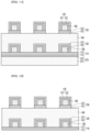
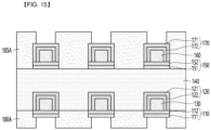
- FIGS. 3 to 15 are views showing the manufacturing method of the circuit board shown in FIG. 1 in order of process.
- a carrier board 210 serving as a basic material is prepared for manufacturing a circuit board.
- the carrier board 210 may include an insulating member 211 and a metal layer 212 disposed on the insulating member 211.
- the metal layer 212 is disposed only on one surface of the insulating member 211 in the drawing, the embodiment is not limited thereto. That is, the metal layer 212 may be disposed on both sides of the insulating member 211, and accordingly, a plurality of circuit boards may be simultaneously manufactured on both sides of the insulating member 211.
- a first-first portion 110 constituting a first barrier layer is formed on the carrier board 210.
- the first-first portion 110 of the first barrier layer may include a first-first metal layer 111 disposed on the carrier board 210 and a first-second metal layer 112 disposed on the first-first metal layer 111.
- the first-first metal layer 111 may include palladium.
- the first-second metal layer 112 may include gold.
- the first-first metal layer 111 and the first-second metal layer 112 may be formed through a chemical copper plating process.
- a first mask M1 of the embodiment is formed on the first-first portion 110 of the first barrier layer.
- the first mask M1 may include an opening (not shown) exposing a region where the first circuit pattern 130 is to be formed.
- a first circuit pattern 130 filling an opening of the first mask M1 of the embodiment is formed by plating a first portion of the first barrier layer as a seed layer.
- the first mask M1 is removed, and a second mask M2 is formed on the first-first portion 110 of the first barrier layer.
- the second mask M2 may include an opening (not shown) exposing a region in which the second-second metal layer 122 is to be formed among the first-second portion 120 of the first barrier layer.
- a second-second metal layer 122 filling the opening of the second mask M2 of the embodiment is formed by plating the first-first portion 110 of the first barrier layer as a seed layer.
- the third mask M3 may include an opening (not shown) exposing a region in which the second-first metal layer 121 is to be formed among the first-second portion 120 of the first barrier layer.
- a second-first metal layer 121 filling the opening of the third mask M3 of the embodiment is formed by plating the first-first portion 110 of the first barrier layer as a seed layer.
- an insulating layer 140 covering the first circuit pattern 130 is formed on the first barrier layer.
- a second-first portion 150 constituting a second barrier layer is formed on the insulating layer 140.
- the second-first portion 150 of the second barrier layer includes a third-first metal layer 151 disposed on the insulating layer 140 and a third-second metal layer 152 disposed on the third-first metal layer 151.
- the third-first metal layer 151 may include palladium. Also, the third-second metal layer 152 may include gold. The third-first metal layer 151 and the third-second metal layer 152 may be formed through a chemical copper plating process.
- a second circuit pattern 160 is formed on the second-first portion 150 of the second barrier layer, and a second-second portion 170 of the second barrier layer is formed on the second circuit pattern 160 by sequentially re-performing the processes of FIGS. 5 to 7 .
- a second-second portion 170 of the second barrier layer includes a fourth-first metal layer 171 and a four-second metal layer 172.
- a process of removing a part of the second-first portion 150 of the second barrier layer may be performed.
- a process of removing the carrier board 210 may be performed.
- a process of removing a part of the first-first portion 110 of the first barrier layer may be performed.
- a process of forming the first protective layer 180 on the lower surface of the insulating layer 140 and forming the second protective layer 185 on the upper surface of the insulating layer 140 may be performed.
- the first protective layer 180 is disposed under the lower surface of the insulating layer 140.
- the second protective layer 185 is disposed on the upper surface of the insulating layer 140.
- the first protective layer 180 and the second protective layer 182 may be formed of at least one layer using any one or more of Solder Resist (SR), oxide, and Au.
- SR Solder Resist
- the first protective layer 180 and the second protective layer 185 may be solder resist.
- the first protective layer 180A may include an opening (not shown) exposing a part of the first-first portion 110 of the first barrier layer.
- the second protective layer 185A may include an opening exposing a part of the second-second portion 170 of the second barrier layer.
- a first barrier layer surrounding the first circuit pattern 130 and a second barrier layer surrounding the second circuit pattern 160 in the embodiment may be formed.
Landscapes
- Engineering & Computer Science (AREA)
- Microelectronics & Electronic Packaging (AREA)
- Manufacturing & Machinery (AREA)
- Parts Printed On Printed Circuit Boards (AREA)
- Manufacturing Of Printed Wiring (AREA)
- Structure Of Printed Boards (AREA)
Applications Claiming Priority (2)
| Application Number | Priority Date | Filing Date | Title |
|---|---|---|---|
| KR1020200060679A KR20210143999A (ko) | 2020-05-21 | 2020-05-21 | 인쇄회로기판 및 이의 제조 방법 |
| PCT/KR2021/006308 WO2021235877A1 (ko) | 2020-05-21 | 2021-05-21 | 회로 기판 |
Publications (2)
| Publication Number | Publication Date |
|---|---|
| EP4156871A1 true EP4156871A1 (en) | 2023-03-29 |
| EP4156871A4 EP4156871A4 (en) | 2024-07-10 |
Family
ID=78708670
Family Applications (1)
| Application Number | Title | Priority Date | Filing Date |
|---|---|---|---|
| EP21808883.9A Pending EP4156871A4 (en) | 2020-05-21 | 2021-05-21 | PRINTED CIRCUIT BOARD |
Country Status (6)
| Country | Link |
|---|---|
| US (1) | US20230199944A1 (ko) |
| EP (1) | EP4156871A4 (ko) |
| JP (1) | JP2023526651A (ko) |
| KR (1) | KR20210143999A (ko) |
| CN (1) | CN116137969A (ko) |
| WO (1) | WO2021235877A1 (ko) |
Family Cites Families (6)
| Publication number | Priority date | Publication date | Assignee | Title |
|---|---|---|---|---|
| US5038195A (en) * | 1990-02-09 | 1991-08-06 | Ibm | Composition and coating to prevent current induced electrochemical dendrite formation between conductors on dielectric substrate |
| JP2001024295A (ja) * | 1999-07-06 | 2001-01-26 | Sony Corp | プリント配線板およびその形成方法 |
| KR20120012348A (ko) * | 2010-07-30 | 2012-02-09 | 엘지이노텍 주식회사 | 인쇄회로기판 및 그의 제조 방법 |
| JP2016085998A (ja) * | 2013-02-19 | 2016-05-19 | パナソニック株式会社 | 半導体装置及びその製造方法 |
| KR102334181B1 (ko) * | 2016-03-25 | 2021-12-03 | 쇼와덴코머티리얼즈가부시끼가이샤 | 유기 인터포저 및 유기 인터포저의 제조 방법 |
| JP6563366B2 (ja) * | 2016-06-13 | 2019-08-21 | 新光電気工業株式会社 | 配線基板及びその製造方法 |
-
2020
- 2020-05-21 KR KR1020200060679A patent/KR20210143999A/ko unknown
-
2021
- 2021-05-21 EP EP21808883.9A patent/EP4156871A4/en active Pending
- 2021-05-21 JP JP2022571281A patent/JP2023526651A/ja active Pending
- 2021-05-21 CN CN202180060531.8A patent/CN116137969A/zh active Pending
- 2021-05-21 US US17/926,681 patent/US20230199944A1/en active Pending
- 2021-05-21 WO PCT/KR2021/006308 patent/WO2021235877A1/ko unknown
Also Published As
| Publication number | Publication date |
|---|---|
| CN116137969A (zh) | 2023-05-19 |
| WO2021235877A1 (ko) | 2021-11-25 |
| US20230199944A1 (en) | 2023-06-22 |
| JP2023526651A (ja) | 2023-06-22 |
| EP4156871A4 (en) | 2024-07-10 |
| KR20210143999A (ko) | 2021-11-30 |
Similar Documents
| Publication | Publication Date | Title |
|---|---|---|
| KR20210114196A (ko) | 인쇄회로기판 및 이의 제조 방법 | |
| EP4167691A1 (en) | Circuit board | |
| KR20210154450A (ko) | 인쇄회로기판 및 이의 제조 방법 | |
| EP4156871A1 (en) | Circuit board | |
| US12089329B2 (en) | Printed circuit board comprising via portions | |
| US20220346236A1 (en) | Printed circuit board | |
| US20230049806A1 (en) | Circuit board | |
| KR20220080306A (ko) | 회로기판의 제조 방법 및 이에 의해 제조된 회로기판 | |
| EP4152900A1 (en) | Circuit board | |
| CN114762463A (zh) | 印刷电路板 | |
| US20240314937A1 (en) | Circuit board | |
| US11778741B2 (en) | Circuit board | |
| KR20200087511A (ko) | 인쇄회로기판 및 이를 포함하는 안테나 모듈 | |
| US20230199959A1 (en) | Circuit board | |
| KR20240100898A (ko) | 안테나 기판 및 이를 포함하는 안테나 패키지 | |
| US20220418107A1 (en) | Printed circuit board | |
| US20230337366A1 (en) | Circuit board and manufacturing method thereof | |
| US20240063104A1 (en) | Circuit board | |
| US20230403790A1 (en) | Circuit board | |
| EP4436322A1 (en) | Circuit board and semiconductor package comprising same | |
| EP4290985A1 (en) | Semiconductor package | |
| KR20210146030A (ko) | 패키지기판 및 이의 제조 방법 | |
| CN117099488A (zh) | 半导体封装 | |
| KR20240127151A (ko) | 회로 기판 및 이를 포함하는 반도체 패키지 | |
| KR20210070024A (ko) | 인쇄회로기판 및 이의 제조 방법 |
Legal Events
| Date | Code | Title | Description |
|---|---|---|---|
| STAA | Information on the status of an ep patent application or granted ep patent |
Free format text: STATUS: THE INTERNATIONAL PUBLICATION HAS BEEN MADE |
|
| PUAI | Public reference made under article 153(3) epc to a published international application that has entered the european phase |
Free format text: ORIGINAL CODE: 0009012 |
|
| STAA | Information on the status of an ep patent application or granted ep patent |
Free format text: STATUS: REQUEST FOR EXAMINATION WAS MADE |
|
| 17P | Request for examination filed |
Effective date: 20221215 |
|
| AK | Designated contracting states |
Kind code of ref document: A1 Designated state(s): AL AT BE BG CH CY CZ DE DK EE ES FI FR GB GR HR HU IE IS IT LI LT LU LV MC MK MT NL NO PL PT RO RS SE SI SK SM TR |
|
| DAV | Request for validation of the european patent (deleted) | ||
| DAX | Request for extension of the european patent (deleted) | ||
| REG | Reference to a national code |
Ref country code: DE Ref legal event code: R079 Free format text: PREVIOUS MAIN CLASS: H05K0001020000 Ipc: H05K0001090000 |
|
| A4 | Supplementary search report drawn up and despatched |
Effective date: 20240611 |
|
| RIC1 | Information provided on ipc code assigned before grant |
Ipc: H05K 3/02 20060101ALN20240606BHEP Ipc: H05K 3/28 20060101ALN20240606BHEP Ipc: H05K 3/00 20060101ALN20240606BHEP Ipc: H05K 3/18 20060101ALI20240606BHEP Ipc: H05K 3/24 20060101ALI20240606BHEP Ipc: H05K 1/09 20060101AFI20240606BHEP |