EP4156480A1 - Stromumwandlungsvorrichtung - Google Patents
Stromumwandlungsvorrichtung Download PDFInfo
- Publication number
- EP4156480A1 EP4156480A1 EP21807658.6A EP21807658A EP4156480A1 EP 4156480 A1 EP4156480 A1 EP 4156480A1 EP 21807658 A EP21807658 A EP 21807658A EP 4156480 A1 EP4156480 A1 EP 4156480A1
- Authority
- EP
- European Patent Office
- Prior art keywords
- heat capacity
- power conversion
- heating element
- high heat
- conversion apparatus
- Prior art date
- Legal status (The legal status is an assumption and is not a legal conclusion. Google has not performed a legal analysis and makes no representation as to the accuracy of the status listed.)
- Pending
Links
Images




Classifications
-
- H—ELECTRICITY
- H05—ELECTRIC TECHNIQUES NOT OTHERWISE PROVIDED FOR
- H05K—PRINTED CIRCUITS; CASINGS OR CONSTRUCTIONAL DETAILS OF ELECTRIC APPARATUS; MANUFACTURE OF ASSEMBLAGES OF ELECTRICAL COMPONENTS
- H05K7/00—Constructional details common to different types of electric apparatus
- H05K7/20—Modifications to facilitate cooling, ventilating, or heating
- H05K7/2089—Modifications to facilitate cooling, ventilating, or heating for power electronics, e.g. for inverters for controlling motor
- H05K7/209—Heat transfer by conduction from internal heat source to heat radiating structure
-
- H—ELECTRICITY
- H02—GENERATION; CONVERSION OR DISTRIBUTION OF ELECTRIC POWER
- H02M—APPARATUS FOR CONVERSION BETWEEN AC AND AC, BETWEEN AC AND DC, OR BETWEEN DC AND DC, AND FOR USE WITH MAINS OR SIMILAR POWER SUPPLY SYSTEMS; CONVERSION OF DC OR AC INPUT POWER INTO SURGE OUTPUT POWER; CONTROL OR REGULATION THEREOF
- H02M1/00—Details of apparatus for conversion
- H02M1/32—Means for protecting converters other than automatic disconnection
- H02M1/327—Means for protecting converters other than automatic disconnection against abnormal temperatures
-
- H—ELECTRICITY
- H05—ELECTRIC TECHNIQUES NOT OTHERWISE PROVIDED FOR
- H05K—PRINTED CIRCUITS; CASINGS OR CONSTRUCTIONAL DETAILS OF ELECTRIC APPARATUS; MANUFACTURE OF ASSEMBLAGES OF ELECTRICAL COMPONENTS
- H05K5/00—Casings, cabinets or drawers for electric apparatus
- H05K5/02—Details
- H05K5/0209—Thermal insulation, e.g. for fire protection or for fire containment or for high temperature environments
- H05K5/0211—Thermal buffers, e.g. latent heat absorbers
-
- H—ELECTRICITY
- H02—GENERATION; CONVERSION OR DISTRIBUTION OF ELECTRIC POWER
- H02M—APPARATUS FOR CONVERSION BETWEEN AC AND AC, BETWEEN AC AND DC, OR BETWEEN DC AND DC, AND FOR USE WITH MAINS OR SIMILAR POWER SUPPLY SYSTEMS; CONVERSION OF DC OR AC INPUT POWER INTO SURGE OUTPUT POWER; CONTROL OR REGULATION THEREOF
- H02M3/00—Conversion of DC power input into DC power output
- H02M3/003—Constructional details, e.g. physical layout, assembly, wiring or busbar connections
-
- H—ELECTRICITY
- H02—GENERATION; CONVERSION OR DISTRIBUTION OF ELECTRIC POWER
- H02M—APPARATUS FOR CONVERSION BETWEEN AC AND AC, BETWEEN AC AND DC, OR BETWEEN DC AND DC, AND FOR USE WITH MAINS OR SIMILAR POWER SUPPLY SYSTEMS; CONVERSION OF DC OR AC INPUT POWER INTO SURGE OUTPUT POWER; CONTROL OR REGULATION THEREOF
- H02M7/00—Conversion of AC power input into DC power output; Conversion of DC power input into AC power output
- H02M7/003—Constructional details, e.g. physical layout, assembly, wiring or busbar connections
-
- H—ELECTRICITY
- H05—ELECTRIC TECHNIQUES NOT OTHERWISE PROVIDED FOR
- H05K—PRINTED CIRCUITS; CASINGS OR CONSTRUCTIONAL DETAILS OF ELECTRIC APPARATUS; MANUFACTURE OF ASSEMBLAGES OF ELECTRICAL COMPONENTS
- H05K1/00—Printed circuits
- H05K1/02—Details
- H05K1/0201—Thermal arrangements, e.g. for cooling, heating or preventing overheating
- H05K1/0203—Cooling of mounted components
-
- H—ELECTRICITY
- H05—ELECTRIC TECHNIQUES NOT OTHERWISE PROVIDED FOR
- H05K—PRINTED CIRCUITS; CASINGS OR CONSTRUCTIONAL DETAILS OF ELECTRIC APPARATUS; MANUFACTURE OF ASSEMBLAGES OF ELECTRICAL COMPONENTS
- H05K1/00—Printed circuits
- H05K1/02—Details
- H05K1/0201—Thermal arrangements, e.g. for cooling, heating or preventing overheating
- H05K1/0203—Cooling of mounted components
- H05K1/0207—Cooling of mounted components using internal conductor planes parallel to the surface for thermal conduction, e.g. power planes
-
- H—ELECTRICITY
- H05—ELECTRIC TECHNIQUES NOT OTHERWISE PROVIDED FOR
- H05K—PRINTED CIRCUITS; CASINGS OR CONSTRUCTIONAL DETAILS OF ELECTRIC APPARATUS; MANUFACTURE OF ASSEMBLAGES OF ELECTRICAL COMPONENTS
- H05K1/00—Printed circuits
- H05K1/02—Details
- H05K1/0201—Thermal arrangements, e.g. for cooling, heating or preventing overheating
- H05K1/0203—Cooling of mounted components
- H05K1/021—Components thermally connected to metal substrates or heat-sinks by insert mounting
-
- H—ELECTRICITY
- H05—ELECTRIC TECHNIQUES NOT OTHERWISE PROVIDED FOR
- H05K—PRINTED CIRCUITS; CASINGS OR CONSTRUCTIONAL DETAILS OF ELECTRIC APPARATUS; MANUFACTURE OF ASSEMBLAGES OF ELECTRICAL COMPONENTS
- H05K2201/00—Indexing scheme relating to printed circuits covered by H05K1/00
- H05K2201/06—Thermal details
- H05K2201/062—Means for thermal insulation, e.g. for protection of parts
-
- H—ELECTRICITY
- H05—ELECTRIC TECHNIQUES NOT OTHERWISE PROVIDED FOR
- H05K—PRINTED CIRCUITS; CASINGS OR CONSTRUCTIONAL DETAILS OF ELECTRIC APPARATUS; MANUFACTURE OF ASSEMBLAGES OF ELECTRICAL COMPONENTS
- H05K2201/00—Indexing scheme relating to printed circuits covered by H05K1/00
- H05K2201/06—Thermal details
- H05K2201/066—Heatsink mounted on the surface of the printed circuit board [PCB]
-
- H—ELECTRICITY
- H05—ELECTRIC TECHNIQUES NOT OTHERWISE PROVIDED FOR
- H05K—PRINTED CIRCUITS; CASINGS OR CONSTRUCTIONAL DETAILS OF ELECTRIC APPARATUS; MANUFACTURE OF ASSEMBLAGES OF ELECTRICAL COMPONENTS
- H05K7/00—Constructional details common to different types of electric apparatus
- H05K7/20—Modifications to facilitate cooling, ventilating, or heating
- H05K7/2039—Modifications to facilitate cooling, ventilating, or heating characterised by the heat transfer by conduction from the heat generating element to a dissipating body
- H05K7/205—Heat-dissipating body thermally connected to heat generating element via thermal paths through printed circuit board [PCB]
-
- H—ELECTRICITY
- H10—SEMICONDUCTOR DEVICES; ELECTRIC SOLID-STATE DEVICES NOT OTHERWISE PROVIDED FOR
- H10W—GENERIC PACKAGES, INTERCONNECTIONS, CONNECTORS OR OTHER CONSTRUCTIONAL DETAILS OF DEVICES COVERED BY CLASS H10
- H10W40/00—Arrangements for thermal protection or thermal control
-
- H—ELECTRICITY
- H10—SEMICONDUCTOR DEVICES; ELECTRIC SOLID-STATE DEVICES NOT OTHERWISE PROVIDED FOR
- H10W—GENERIC PACKAGES, INTERCONNECTIONS, CONNECTORS OR OTHER CONSTRUCTIONAL DETAILS OF DEVICES COVERED BY CLASS H10
- H10W40/00—Arrangements for thermal protection or thermal control
- H10W40/20—Arrangements for cooling
- H10W40/22—Arrangements for cooling characterised by their shape, e.g. having conical or cylindrical projections
-
- H—ELECTRICITY
- H10—SEMICONDUCTOR DEVICES; ELECTRIC SOLID-STATE DEVICES NOT OTHERWISE PROVIDED FOR
- H10W—GENERIC PACKAGES, INTERCONNECTIONS, CONNECTORS OR OTHER CONSTRUCTIONAL DETAILS OF DEVICES COVERED BY CLASS H10
- H10W40/00—Arrangements for thermal protection or thermal control
- H10W40/20—Arrangements for cooling
- H10W40/231—Arrangements for cooling characterised by their places of attachment or cooling paths
-
- H—ELECTRICITY
- H10—SEMICONDUCTOR DEVICES; ELECTRIC SOLID-STATE DEVICES NOT OTHERWISE PROVIDED FOR
- H10W—GENERIC PACKAGES, INTERCONNECTIONS, CONNECTORS OR OTHER CONSTRUCTIONAL DETAILS OF DEVICES COVERED BY CLASS H10
- H10W40/00—Arrangements for thermal protection or thermal control
- H10W40/20—Arrangements for cooling
- H10W40/25—Arrangements for cooling characterised by their materials
Definitions
- the present disclosure relates to the technical field of heat dissipation in power electronics, and in particular to a power conversion apparatus.
- a system not only requires a power conversion apparatus to meet a rated condition, but also requires the power conversion apparatus to provide an output capacity several times higher than a peak in the rated condition in a short period of time.
- loss of a heating element in the power conversion apparatus increases exponentially, resulting in a great impact on devices such as a power semiconductor device in the power conversion apparatus .
- the power semiconductor device for example, a wafer
- the power semiconductor device is small in size, and is to be industrially packaged in order to be made into a finished product, thus the finished product is also small in size.
- the power semiconductor device is isolated from a heat dissipation device by an insulating material for the sake of electrical insulation, and the insulating material generally has a poor thermal conductivity. Therefore, a great loss of the power semiconductor device in a short period of time inevitably results in a sharp rise in a temperature of the power semiconductor device, greatly impacting the power semiconductor device and further reducing operation reliability of the system.
- a switch transistor with high performance is generally adopted or multiple switch transistors are connected in parallel to reduce power consumption at the peak, thereby reducing a rate at which the temperature of the power semiconductor device rises.
- the insulating material is replaced with a material of a high thermal conductivity, such as an aluminum substrate and a thermally conductive silicone grease, to speed up heat transfer from the power semiconductor device to the heat dissipation device.
- a heat dissipation device with a high heat dissipation capacity may be adopted to reduce the temperature of the power conversion apparatus itself.
- a power conversion apparatus is provided according to an embodiment of the present disclosure, to solve the problem existing in the conventional technology that the system is large in size and weight, and has high costs.
- a power conversion apparatus includes: a low thermal resistance path, a high thermal resistance path, a heatsink, an additional high heat capacity device, and at least one heating element.
- the additional high heat capacity device is connected to the at least one heating element via the low thermal resistance path.
- the heatsink is connected to the at least one heating element via the high thermal resistance path.
- the low thermal resistance path is made of one kind of metal or multiple kinds of metal.
- the additional high heat capacity device is made of metal.
- the additional high heat capacity device is made of copper or aluminum.
- the additional high heat capacity device is in a shape of a strip or a block.
- the additional high heat capacity device is arranged around the at least one heating element, or the additional high heat capacity device is arranged to straddle the at least one heating element.
- each of the at least one heating element includes a power device chip arranged on a chip lead frame.
- the low thermal resistance path is formed by a surface metal of a PCB and solder for the surface metal. Multiple heating elements form a power conversion circuit on the PCB.
- the power conversion circuit is an ACDC conversion circuit, a DCAC conversion circuit, a DCDC conversion circuit or an ACAC conversion circuit.
- the high thermal resistance path includes at least one insulating layer.
- the additional high heat capacity device is connected to the heating element via the low thermal resistance path, such that the heat capacity of the heating element 202 is increased. Therefore, in a case that the temperature of the heating element rises rapidly due to a large transient loss, the rate at which the temperature of the heating element rises is reduced, such that the temperature of the heating element at the end of the peak condition in a short period of time is lowered, thereby ensuring reliability of the power conversion apparatus.
- FIG. 1 is a schematic diagram illustrating a heating element to a heat dissipation device in cross-section according to the conventional technology.
- a heating element 101 inevitably generates a large amount of heat in a short period of time (for example, tens of seconds) in order to meet an output condition at a peak, that is, an output capacity several times higher than that at the rated condition.
- the heat is transferred to a heat dissipation device 105 through a semiconductor lead frame 102, a PCB (Printed Circuit Board) surface copper foil 103 and a PCB insulating layer 104 in sequence.
- PCB Printed Circuit Board
- the heat dissipation device 105 fails to achieve a good heat dissipation effect, resulting in a sharp rise in temperature of the heating element 101, which has a great impact on the system.
- a power conversion apparatus is provided according to the present disclosure, to solve the problem of large size, large weight and high costs of the system existing in the conventional technology.
- FIG. 2 schematically illustrates the apparatus in cross-section.
- the power conversion apparatus includes: a low thermal resistance path 203, a high thermal resistance path 204, a heatsink 205, an additional high heat capacity device 201 and at least one heating element 202.
- the additional high heat capacity device 201 is connected to the at least one heating element 202 via the low thermal resistance path 203.
- the heatsink 205 is connected to the at least one heating element 202 via the high thermal resistance path 204.
- the power conversion apparatus includes one heating element 202.
- Figure 3 illustrates a top view of the heating element 202.
- the heating element 202 includes a power device chip 302 arranged on a chip lead frame 301.
- the chip lead frame 301 is generally implemented by a DBC (Direct Bonded Copper) board.
- the power device chip 302 is soldered on one side of the chip lead frame 301, and then the power device chip 302 and the chip lead frame 301 are packaged by using materials such as epoxy to form a device. Due to the limitation of industrial packaging standards, the power device chip 302 is generally small in size, and the chip lead frame 301 is also generally small in size on which a size of the packaged device depends.
- the low thermal resistance path 203 is made of one kind of metal or multiple kinds of metal, for example, a surface metal of the PCB (including an aluminum substrate) and solder for the surface metal.
- the surface metal of the PCB is generally made of copper foil. Since the copper is prone to oxidation in common environment, it is impossible to apply tin on the surface metal (of poor solderability). Therefore, the copper surface is protected by processes such as hot air solder leveling (HASL), electroless nickel immersion gold (ENIG), immersion silver, immersion tin, and organic solderability preservative (OSP). These processes are not limited herein.
- HSL hot air solder leveling
- ENIG electroless nickel immersion gold
- immersion silver immersion tin
- OSP organic solderability preservative
- multiple heating elements 202 for example, a heating element 1 to a heating element 5 in Figure 4 , are generally soldered to the copper foil printed on the PCB.
- the multiple heating elements 202 form a power conversion circuit, by soldering and wiring, on the copper foil printed on the PBC.
- the power conversion circuit may be an ACDC conversion circuit, a DCAC conversion circuit, a DCDC conversion circuit, or an ACAC conversion circuit, depending on application scenarios.
- the additional high heat capacity device 201 is arranged in a manner similar to that in the case of only one heating element 202.
- the additional high heat capacity device 201 may be implemented as a whole or as multiple separate elements, which is not limited herein.
- the copper foil on the PCB is of tens of microns in thickness, and is small in area for the sake of power density, and thus is small in size.
- the heating element 202 itself is small in size, and the low thermal resistance path 203 is also small in size, leading to a relatively low overall heat capacity of the system.
- the high thermal resistance path 204 includes at least one insulating layer, which may actually be an insulating layer in the aluminum substrate and the heat conductive silicone grease and the like. It is well known that the insulating layer and the heat conductive silicone grease each have low thermal conductivity, even less than one percent of the metal for the chip lead frame 301, the PCB and the like.
- the insulating layer generally has a certain thickness in order to ensure insulation performance and processing performance (for example, anti-breakage or anti-cracking) of the insulating layer.
- the heating element 202 of small heat capacity is arranged on the low thermal resistance path 203, and then the low thermal resistance path 203 is arranged on the heatsink 205 via the high thermal resistance path 204, the heating element 202 generates a large amount of heat in response to a large amount of power consumption in a short period of time.
- the heat is transferred to the heatsink 205 through the high thermal resistance path 204, and on the other hand the heat is shared between the heating element 202 and the PCB.
- the overall heat capacity is small and the rate at which the heat is transferred to the heatsink 205 through the high thermal resistance path 204 is slow, inevitably resulting in a sharp rise in temperature of the heating element 202, thereby affecting the reliability of the apparatus.
- the additional high heat capacity device 201 is connected to the heating element 202 though the low thermal resistance path 203.
- the additional high heat capacity device 201 is large in size, leading to an increase in heat capacity of the heating element 202. Therefore, the rise in temperature of the heating element 202 is slowed down in a case that the power device chip 302 causes a large amount of power consumption in a short period of time.
- the additional high heat capacity device 201 is connected to the heating element 202 via the low thermal resistance path 203.
- the solution that the additional high heat capacity device 201 is arranged on the PCB and around the heating element 202 and the solution that the additional high heat capacity device 201 is interspersed among multiple heating elements 202 are all within the protection scope of the present disclosure.
- the additional high heat capacity device 201 is generally made of metal with relatively high thermal conductivity, including but not limited to copper or aluminum. Any solution that the additional high heat capacity device 201 is made of material with thermal conductivity greater than that of the high thermal resistance path 204 is within the protection scope of the present disclosure.
- a metal of high heat capacity is soldered on the edge of the copper foil to reduce the instantaneous rise in temperature.
- the additional high heat capacity device 201 may be in the shape of a strip or a block.
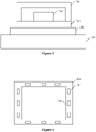
- Figure 6 is a top view illustrating the additional high heat capacity device 201 in the shape of a block
- Figure 7 is a top view illustrating the additional high heat capacity device 201 in the shape of a strip.
- the additional high heat capacity device 201 in the shape of either the strip or the block may be arranged around the heating element 202 (as shown in Figure 6 and Figure 7 ) or interspersed among multiple heating elements 202 (not shown).
- the additional high heat capacity device 201 is in the shape of a strip
- the additional high heat capacity device 201 is in the shape of a U-shaped strip.
- Figure 8 is a top view illustrating the additional high heat capacity device 201 in the shape of a U-shaped strip.
- the additional high heat capacity device 201 in the shape of a U-shaped strip is soldered on the copper foil printed on the PCB with the opening facing down, straddling the heating element 202, as shown in Figure 5 in cross-section.
- Figure 6 to Figure 8 each illustrate an example in which the number of the additional high heat capacity device 201 is multiple.
- the power conversion apparatus may include one additional high heat capacity device 201, which is not limited herein.
- One or more copper blocks or copper strips may be arranged depending on application scenarios, which are all within the protection scope of the present disclosure.
- the additional high heat capacity device 201 is soldered on the copper foil printed on the PCB board for the following reasons.
- the chip lead frame 301 to which the heating element 202 is soldered is small in size, and has no room for the additional high heat capacity device 201.
- the additional high heat capacity device 201 being soldered to the chip lead frame 301 inevitably results in an increase in size and weight of the heating element 202, which is not in line with the original intention of the present disclosure.
- the additional high heat capacity device 201 in any shape that increasing the heat capacity of the heating element 202 is within the protection scope of the present disclosure.
- a copper strip or a copper block is soldered on the copper foil printed on the PCB and around the power component chip 302, such that the temperature at the peak is reduced.
- the operation principle of the additional high heat capacity device 201 is explained based on the following formula for heat energy and formula for thermal conduction.
- q represents absorbed or released thermal energy (J).
- c represents the specific heat capacity of the material (J/(kg.°C)).
- m represents mass of the material (kg).
- ⁇ T represents a difference in temperature (°C).
- Q represents the heat conduction flow (W).
- ⁇ represents thermal conductivity (W/m.°C) of the material.
- A represents the cross-sectional area (m 2 ) perpendicular to the direction of heat transfer.
- ⁇ t ⁇ x represents a temperature gradient (°C/m) along a normal line to the isothermal surface.
- the negative sign in the formula indicates that the direction of heat transfer is opposite to the temperature gradient. It can be seen that in order to increase the amount of heat dissipated through heat transfer, the thermal conductivity of the material is increased. For example, a material with high thermal conductivity (copper or aluminum) is selected. Alternatively, a cross-sectional area of the additional high heat capacity device 201 in the direction of heat transfer is increased.
- the additional high heat capacity device is connected to the heating element via the low thermal resistance path, such that the heat capacity of the heating element 202 is increased. Therefore, in a case that the temperature of the heating element rises rapidly due to a large transient loss, the rate at which the temperature of the heating element rises is reduced, such that the temperature of the heating element at the end of the peak condition in a short period of time is lowered, thereby ensuring the reliability of the power conversion apparatus.
- the power conversion apparatus with an additional heat capacity apparatus 201 has a significant effect on reducing the rate at which the temperature of the system rises in a case that the temperature of the heating element 202 rises rapidly due to a large transient loss.
- a starting point of the curve indicates that the temperature of the heating element 202 begins to rise rapidly. It can be seen that the temperature of the system with no additional high heat capacity device or other better heat dissipation device in the conventional technology rises rapidly.
- the rate at which the temperature of the system with an additional high heat capacity device according to this embodiment rises is significantly lower than that of the system with no additional high heat capacity device.
- the temperature of the system with an additional high heat capacity device is also significantly lower than that of the system with no additional high heat capacity device, which proves the rationality and feasibility of the system with an additional high heat capacity device and ensures the reliability of the system.
- a switch transistor with a high performance is adopted or multiple switch transistors are connected in parallel in the system to reduce the peak power consumption of the system, thereby reducing the rate at which the temperature of the heating component rises.
- a material with high thermal conductivity such as an aluminum substrate and a heat conductive silicone grease is selected to accelerate the transfer of the heat generated by the heating element to the heatsink.
- a heat dissipation device with high heat dissipation capacity is arranged to reduce the temperature of the system itself.
- an additional high heat capacity device 201 is arranged on the low thermal resistance path 203, such that the heat capacity of the heating element 202 is increased, thereby increasing the ability of the heating element 202 to store heat at the peak condition without changing the rise in the temperature in the rated condition.
- no change is made to the heating element or the heat dissipation device, leading to no increase in the size or weight as well as the costs of the system.
Landscapes
- Engineering & Computer Science (AREA)
- Microelectronics & Electronic Packaging (AREA)
- Power Engineering (AREA)
- Physics & Mathematics (AREA)
- Thermal Sciences (AREA)
- Cooling Or The Like Of Semiconductors Or Solid State Devices (AREA)
- Cooling Or The Like Of Electrical Apparatus (AREA)
- Power Conversion In General (AREA)
- Inverter Devices (AREA)
Applications Claiming Priority (2)
| Application Number | Priority Date | Filing Date | Title |
|---|---|---|---|
| CN202020837107.2U CN211908640U (zh) | 2020-05-19 | 2020-05-19 | 一种功率变换装置 |
| PCT/CN2021/094057 WO2021233241A1 (zh) | 2020-05-19 | 2021-05-17 | 一种功率变换装置 |
Publications (2)
| Publication Number | Publication Date |
|---|---|
| EP4156480A1 true EP4156480A1 (de) | 2023-03-29 |
| EP4156480A4 EP4156480A4 (de) | 2024-06-05 |
Family
ID=73270243
Family Applications (1)
| Application Number | Title | Priority Date | Filing Date |
|---|---|---|---|
| EP21807658.6A Pending EP4156480A4 (de) | 2020-05-19 | 2021-05-17 | Stromumwandlungsvorrichtung |
Country Status (5)
| Country | Link |
|---|---|
| US (1) | US20230108943A1 (de) |
| EP (1) | EP4156480A4 (de) |
| JP (1) | JP3242452U (de) |
| CN (1) | CN211908640U (de) |
| WO (1) | WO2021233241A1 (de) |
Families Citing this family (1)
| Publication number | Priority date | Publication date | Assignee | Title |
|---|---|---|---|---|
| CN211908640U (zh) * | 2020-05-19 | 2020-11-10 | 阳光电源股份有限公司 | 一种功率变换装置 |
Family Cites Families (22)
| Publication number | Priority date | Publication date | Assignee | Title |
|---|---|---|---|---|
| FI88452C (fi) * | 1990-03-29 | 1993-05-10 | Nokia Mobile Phones Ltd | Konstruktion foer att foerbaettra avkylning av en effekttransistor |
| DE4232575A1 (de) * | 1992-09-29 | 1994-03-31 | Bosch Gmbh Robert | Anordnung mit einer Leiterplatte, mindestens einem Leistungsbauelement und einem Kühlkörper |
| TW546796B (en) * | 2002-06-10 | 2003-08-11 | Advanced Semiconductor Eng | Multichip package |
| JP2004022983A (ja) * | 2002-06-19 | 2004-01-22 | Mitsubishi Electric Corp | 半導体装置 |
| JP2005094842A (ja) * | 2003-09-12 | 2005-04-07 | Toshiba Corp | インバータ装置及びその製造方法 |
| JP2005332874A (ja) * | 2004-05-18 | 2005-12-02 | Hitachi Metals Ltd | 回路基板及びこれを用いた半導体装置 |
| JP2007305702A (ja) * | 2006-05-10 | 2007-11-22 | Toshiba Corp | 半導体装置およびその製造方法 |
| US8164176B2 (en) * | 2006-10-20 | 2012-04-24 | Infineon Technologies Ag | Semiconductor module arrangement |
| KR101469770B1 (ko) * | 2007-11-21 | 2014-12-09 | 페어차일드코리아반도체 주식회사 | 전력 소자 패키지 및 그 제조 방법 |
| DE102007062167A1 (de) * | 2007-12-21 | 2009-06-25 | Robert Bosch Gmbh | Leistungsschaltung |
| EP2265099B1 (de) * | 2009-06-04 | 2013-11-27 | Honda Motor Co., Ltd. | Halbleiterbauelement und Verfahren zu seiner Herstellung |
| EP2276329A1 (de) * | 2009-07-16 | 2011-01-19 | ABB Research Ltd. | Elektronische Platine mit Wärmekondensator |
| US8520389B2 (en) * | 2009-12-02 | 2013-08-27 | Hamilton Sundstrand Corporation | Power semiconductor module for wide temperature applications |
| KR101533895B1 (ko) * | 2010-09-02 | 2015-07-03 | 도요타지도샤가부시키가이샤 | 반도체 모듈 |
| US9099426B2 (en) * | 2011-02-23 | 2015-08-04 | University Of Maryland, College Park | Trench-assisted thermoelectric isothermalization of power switching chips |
| JP2013004953A (ja) * | 2011-06-22 | 2013-01-07 | Denso Corp | 電子制御装置 |
| CN103745962B (zh) * | 2013-12-19 | 2017-05-10 | 联合汽车电子有限公司 | 适用于电动汽车逆变器的igbt模块及封装方法和使用方法 |
| JP6540587B2 (ja) * | 2016-04-28 | 2019-07-10 | 三菱電機株式会社 | パワーモジュール |
| JP6770452B2 (ja) * | 2017-01-27 | 2020-10-14 | ルネサスエレクトロニクス株式会社 | 半導体装置 |
| WO2018207856A1 (ja) * | 2017-05-10 | 2018-11-15 | ローム株式会社 | パワー半導体装置およびその製造方法 |
| JP6394741B1 (ja) * | 2017-05-30 | 2018-09-26 | ダイキン工業株式会社 | 電力変換装置、冷凍装置 |
| CN211908640U (zh) * | 2020-05-19 | 2020-11-10 | 阳光电源股份有限公司 | 一种功率变换装置 |
-
2020
- 2020-05-19 CN CN202020837107.2U patent/CN211908640U/zh active Active
-
2021
- 2021-05-17 EP EP21807658.6A patent/EP4156480A4/de active Pending
- 2021-05-17 WO PCT/CN2021/094057 patent/WO2021233241A1/zh not_active Ceased
- 2021-05-17 JP JP2022600112U patent/JP3242452U/ja active Active
- 2021-05-17 US US17/798,602 patent/US20230108943A1/en not_active Abandoned
Also Published As
| Publication number | Publication date |
|---|---|
| US20230108943A1 (en) | 2023-04-06 |
| EP4156480A4 (de) | 2024-06-05 |
| WO2021233241A1 (zh) | 2021-11-25 |
| JP3242452U (ja) | 2023-06-19 |
| CN211908640U (zh) | 2020-11-10 |
Similar Documents
| Publication | Publication Date | Title |
|---|---|---|
| KR101013001B1 (ko) | 효과적인 열 방출을 위한 선이 없는 반도체 패키지 | |
| US10524349B2 (en) | Printed circuit board with built-in vertical heat dissipation ceramic block, and electrical assembly comprising the board | |
| CN102595768A (zh) | 电路板 | |
| CN210575912U (zh) | 电路板及电子设备 | |
| CN106206493A (zh) | 一种封装芯片的散热结构 | |
| EP4156480A1 (de) | Stromumwandlungsvorrichtung | |
| EP3533303B1 (de) | Leistungsmodul | |
| CN217160294U (zh) | 具有散热器的金属衬底电子元器件 | |
| CN216563091U (zh) | 一种双面散热功率模块 | |
| CN212517183U (zh) | 一种igbt模块高效散热结构 | |
| EP3633720B1 (de) | Oberflächenmontierter wärmepuffer | |
| KR200491106Y1 (ko) | 인터페이스 카드의 다방향 방열 구조 | |
| CN214672591U (zh) | 一种功率器件封装结构 | |
| US6930386B1 (en) | Shock hardened mounting and cooling of a semiconductor device | |
| CN104039112A (zh) | 散热模块 | |
| CN212587483U (zh) | 一种高散热半导体产品及电子产品 | |
| JP2008171963A (ja) | 半導体チップ冷却構造 | |
| CN211210276U (zh) | 一种散热结构 | |
| CN113635648B (zh) | 一种界面导热材料的制备方法 | |
| CN205179511U (zh) | 一种高散热性能的大功率电子元件线路板 | |
| CN113675093A (zh) | 一种双面塑封的散热结构的封装设计及制备方法 | |
| CN221427722U (zh) | 一种碳化硅二极管的封装框架 | |
| CN206432253U (zh) | 半导体器件 | |
| CN222653962U (zh) | 功率模块和功率设备 | |
| CN216700441U (zh) | 一种负载点电源模块 |
Legal Events
| Date | Code | Title | Description |
|---|---|---|---|
| STAA | Information on the status of an ep patent application or granted ep patent |
Free format text: STATUS: THE INTERNATIONAL PUBLICATION HAS BEEN MADE |
|
| PUAI | Public reference made under article 153(3) epc to a published international application that has entered the european phase |
Free format text: ORIGINAL CODE: 0009012 |
|
| STAA | Information on the status of an ep patent application or granted ep patent |
Free format text: STATUS: REQUEST FOR EXAMINATION WAS MADE |
|
| 17P | Request for examination filed |
Effective date: 20220804 |
|
| AK | Designated contracting states |
Kind code of ref document: A1 Designated state(s): AL AT BE BG CH CY CZ DE DK EE ES FI FR GB GR HR HU IE IS IT LI LT LU LV MC MK MT NL NO PL PT RO RS SE SI SK SM TR |
|
| DAV | Request for validation of the european patent (deleted) | ||
| DAX | Request for extension of the european patent (deleted) | ||
| A4 | Supplementary search report drawn up and despatched |
Effective date: 20240506 |
|
| RIC1 | Information provided on ipc code assigned before grant |
Ipc: H05K 5/02 20060101ALI20240429BHEP Ipc: H05K 7/20 20060101ALI20240429BHEP Ipc: H02M 1/00 20060101AFI20240429BHEP |