EP4137624A1 - Verfahren zur herstellung eines aluminiumnitridsubstrats, aluminiumnitridsubstrat und verfahren zur entfernung einer in ein aluminiumnitridsubstrat durch laserbearbeitung eingeführten spannungsschicht - Google Patents
Verfahren zur herstellung eines aluminiumnitridsubstrats, aluminiumnitridsubstrat und verfahren zur entfernung einer in ein aluminiumnitridsubstrat durch laserbearbeitung eingeführten spannungsschicht Download PDFInfo
- Publication number
- EP4137624A1 EP4137624A1 EP21789083.9A EP21789083A EP4137624A1 EP 4137624 A1 EP4137624 A1 EP 4137624A1 EP 21789083 A EP21789083 A EP 21789083A EP 4137624 A1 EP4137624 A1 EP 4137624A1
- Authority
- EP
- European Patent Office
- Prior art keywords
- aluminum nitride
- nitride substrate
- strained layer
- aln substrate
- substrate
- Prior art date
- Legal status (The legal status is an assumption and is not a legal conclusion. Google has not performed a legal analysis and makes no representation as to the accuracy of the status listed.)
- Pending
Links
Images

Classifications
-
- C—CHEMISTRY; METALLURGY
- C30—CRYSTAL GROWTH
- C30B—SINGLE-CRYSTAL GROWTH; UNIDIRECTIONAL SOLIDIFICATION OF EUTECTIC MATERIAL OR UNIDIRECTIONAL DEMIXING OF EUTECTOID MATERIAL; REFINING BY ZONE-MELTING OF MATERIAL; PRODUCTION OF A HOMOGENEOUS POLYCRYSTALLINE MATERIAL WITH DEFINED STRUCTURE; SINGLE CRYSTALS OR HOMOGENEOUS POLYCRYSTALLINE MATERIAL WITH DEFINED STRUCTURE; AFTER-TREATMENT OF SINGLE CRYSTALS OR A HOMOGENEOUS POLYCRYSTALLINE MATERIAL WITH DEFINED STRUCTURE; APPARATUS THEREFOR
- C30B29/00—Single crystals or homogeneous polycrystalline material with defined structure characterised by the material or by their shape
- C30B29/10—Inorganic compounds or compositions
- C30B29/40—AIIIBV compounds wherein A is B, Al, Ga, In or Tl and B is N, P, As, Sb or Bi
- C30B29/403—AIII-nitrides
-
- B—PERFORMING OPERATIONS; TRANSPORTING
- B23—MACHINE TOOLS; METAL-WORKING NOT OTHERWISE PROVIDED FOR
- B23K—SOLDERING OR UNSOLDERING; WELDING; CLADDING OR PLATING BY SOLDERING OR WELDING; CUTTING BY APPLYING HEAT LOCALLY, e.g. FLAME CUTTING; WORKING BY LASER BEAM
- B23K26/00—Working by laser beam, e.g. welding, cutting or boring
- B23K26/08—Devices involving relative movement between laser beam and workpiece
- B23K26/082—Scanning systems, i.e. devices involving movement of the laser beam relative to the laser head
-
- B—PERFORMING OPERATIONS; TRANSPORTING
- B23—MACHINE TOOLS; METAL-WORKING NOT OTHERWISE PROVIDED FOR
- B23K—SOLDERING OR UNSOLDERING; WELDING; CLADDING OR PLATING BY SOLDERING OR WELDING; CUTTING BY APPLYING HEAT LOCALLY, e.g. FLAME CUTTING; WORKING BY LASER BEAM
- B23K26/00—Working by laser beam, e.g. welding, cutting or boring
- B23K26/36—Removing material
- B23K26/38—Removing material by boring or cutting
- B23K26/382—Removing material by boring or cutting by boring
-
- B—PERFORMING OPERATIONS; TRANSPORTING
- B23—MACHINE TOOLS; METAL-WORKING NOT OTHERWISE PROVIDED FOR
- B23K—SOLDERING OR UNSOLDERING; WELDING; CLADDING OR PLATING BY SOLDERING OR WELDING; CUTTING BY APPLYING HEAT LOCALLY, e.g. FLAME CUTTING; WORKING BY LASER BEAM
- B23K26/00—Working by laser beam, e.g. welding, cutting or boring
- B23K26/36—Removing material
- B23K26/38—Removing material by boring or cutting
- B23K26/382—Removing material by boring or cutting by boring
- B23K26/384—Removing material by boring or cutting by boring of specially shaped holes
-
- B—PERFORMING OPERATIONS; TRANSPORTING
- B23—MACHINE TOOLS; METAL-WORKING NOT OTHERWISE PROVIDED FOR
- B23K—SOLDERING OR UNSOLDERING; WELDING; CLADDING OR PLATING BY SOLDERING OR WELDING; CUTTING BY APPLYING HEAT LOCALLY, e.g. FLAME CUTTING; WORKING BY LASER BEAM
- B23K26/00—Working by laser beam, e.g. welding, cutting or boring
- B23K26/36—Removing material
- B23K26/40—Removing material taking account of the properties of the material involved
- B23K26/402—Removing material taking account of the properties of the material involved involving non-metallic material, e.g. isolators
-
- C—CHEMISTRY; METALLURGY
- C30—CRYSTAL GROWTH
- C30B—SINGLE-CRYSTAL GROWTH; UNIDIRECTIONAL SOLIDIFICATION OF EUTECTIC MATERIAL OR UNIDIRECTIONAL DEMIXING OF EUTECTOID MATERIAL; REFINING BY ZONE-MELTING OF MATERIAL; PRODUCTION OF A HOMOGENEOUS POLYCRYSTALLINE MATERIAL WITH DEFINED STRUCTURE; SINGLE CRYSTALS OR HOMOGENEOUS POLYCRYSTALLINE MATERIAL WITH DEFINED STRUCTURE; AFTER-TREATMENT OF SINGLE CRYSTALS OR A HOMOGENEOUS POLYCRYSTALLINE MATERIAL WITH DEFINED STRUCTURE; APPARATUS THEREFOR
- C30B33/00—After-treatment of single crystals or homogeneous polycrystalline material with defined structure
- C30B33/02—Heat treatment
-
- C—CHEMISTRY; METALLURGY
- C30—CRYSTAL GROWTH
- C30B—SINGLE-CRYSTAL GROWTH; UNIDIRECTIONAL SOLIDIFICATION OF EUTECTIC MATERIAL OR UNIDIRECTIONAL DEMIXING OF EUTECTOID MATERIAL; REFINING BY ZONE-MELTING OF MATERIAL; PRODUCTION OF A HOMOGENEOUS POLYCRYSTALLINE MATERIAL WITH DEFINED STRUCTURE; SINGLE CRYSTALS OR HOMOGENEOUS POLYCRYSTALLINE MATERIAL WITH DEFINED STRUCTURE; AFTER-TREATMENT OF SINGLE CRYSTALS OR A HOMOGENEOUS POLYCRYSTALLINE MATERIAL WITH DEFINED STRUCTURE; APPARATUS THEREFOR
- C30B33/00—After-treatment of single crystals or homogeneous polycrystalline material with defined structure
- C30B33/04—After-treatment of single crystals or homogeneous polycrystalline material with defined structure using electric or magnetic fields or particle radiation
-
- C—CHEMISTRY; METALLURGY
- C30—CRYSTAL GROWTH
- C30B—SINGLE-CRYSTAL GROWTH; UNIDIRECTIONAL SOLIDIFICATION OF EUTECTIC MATERIAL OR UNIDIRECTIONAL DEMIXING OF EUTECTOID MATERIAL; REFINING BY ZONE-MELTING OF MATERIAL; PRODUCTION OF A HOMOGENEOUS POLYCRYSTALLINE MATERIAL WITH DEFINED STRUCTURE; SINGLE CRYSTALS OR HOMOGENEOUS POLYCRYSTALLINE MATERIAL WITH DEFINED STRUCTURE; AFTER-TREATMENT OF SINGLE CRYSTALS OR A HOMOGENEOUS POLYCRYSTALLINE MATERIAL WITH DEFINED STRUCTURE; APPARATUS THEREFOR
- C30B33/00—After-treatment of single crystals or homogeneous polycrystalline material with defined structure
- C30B33/08—Etching
-
- H—ELECTRICITY
- H10—SEMICONDUCTOR DEVICES; ELECTRIC SOLID-STATE DEVICES NOT OTHERWISE PROVIDED FOR
- H10P—GENERIC PROCESSES OR APPARATUS FOR THE MANUFACTURE OR TREATMENT OF DEVICES COVERED BY CLASS H10
- H10P50/00—Etching of wafers, substrates or parts of devices
- H10P50/20—Dry etching; Plasma etching; Reactive-ion etching
- H10P50/24—Dry etching; Plasma etching; Reactive-ion etching of semiconductor materials
- H10P50/246—Dry etching; Plasma etching; Reactive-ion etching of semiconductor materials of Group III-V materials
-
- B—PERFORMING OPERATIONS; TRANSPORTING
- B23—MACHINE TOOLS; METAL-WORKING NOT OTHERWISE PROVIDED FOR
- B23K—SOLDERING OR UNSOLDERING; WELDING; CLADDING OR PLATING BY SOLDERING OR WELDING; CUTTING BY APPLYING HEAT LOCALLY, e.g. FLAME CUTTING; WORKING BY LASER BEAM
- B23K2101/00—Articles made by soldering, welding or cutting
- B23K2101/36—Electric or electronic devices
- B23K2101/40—Semiconductor devices
-
- B—PERFORMING OPERATIONS; TRANSPORTING
- B23—MACHINE TOOLS; METAL-WORKING NOT OTHERWISE PROVIDED FOR
- B23K—SOLDERING OR UNSOLDERING; WELDING; CLADDING OR PLATING BY SOLDERING OR WELDING; CUTTING BY APPLYING HEAT LOCALLY, e.g. FLAME CUTTING; WORKING BY LASER BEAM
- B23K2103/00—Materials to be soldered, welded or cut
- B23K2103/50—Inorganic materials other than metals or composite materials
- B23K2103/52—Ceramics
-
- H—ELECTRICITY
- H10—SEMICONDUCTOR DEVICES; ELECTRIC SOLID-STATE DEVICES NOT OTHERWISE PROVIDED FOR
- H10P—GENERIC PROCESSES OR APPARATUS FOR THE MANUFACTURE OR TREATMENT OF DEVICES COVERED BY CLASS H10
- H10P14/00—Formation of materials, e.g. in the shape of layers or pillars
- H10P14/20—Formation of materials, e.g. in the shape of layers or pillars of semiconductor materials
- H10P14/29—Formation of materials, e.g. in the shape of layers or pillars of semiconductor materials characterised by the substrates
- H10P14/2901—Materials
- H10P14/2907—Materials being Group IIIA-VA materials
- H10P14/2908—Nitrides
-
- H—ELECTRICITY
- H10—SEMICONDUCTOR DEVICES; ELECTRIC SOLID-STATE DEVICES NOT OTHERWISE PROVIDED FOR
- H10P—GENERIC PROCESSES OR APPARATUS FOR THE MANUFACTURE OR TREATMENT OF DEVICES COVERED BY CLASS H10
- H10P14/00—Formation of materials, e.g. in the shape of layers or pillars
- H10P14/20—Formation of materials, e.g. in the shape of layers or pillars of semiconductor materials
- H10P14/29—Formation of materials, e.g. in the shape of layers or pillars of semiconductor materials characterised by the substrates
- H10P14/2924—Structures
- H10P14/2925—Surface structures
Definitions
- the present invention relates to a method for manufacturing an aluminum nitride substrate, an aluminum nitride substrate, and a method for removing a strained layer introduced into the aluminum nitride substrate by laser processing.
- Patent Literature 1 discloses an invention in which a converging point of a laser beam having a wavelength with absorbency with respect to an object to be processed is positioned on an upper surface of the object to be processed, the object to be processed is irradiated with the laser beam, and ablation processing is performed to form a groove on the upper surface of the object to be processed. Furthermore, it can be understood that the invention described in Patent Literature 1 is a method that can be applied to a known semiconductor material.
- Patent Literature 1 JP H10-305420 A
- An object of the present invention is to provide a novel technique capable of removing the strained layer introduced into the aluminum nitride substrate.
- the present invention is a method for manufacturing an aluminum nitride substrate, and the method includes a strained layer removal step of removing a strained layer of the aluminum nitride substrate by heat treating the aluminum nitride substrate under a nitrogen atmosphere.
- the strained layer introduced into the aluminum nitride substrate can be removed.
- the strained layer removal step heat treats the aluminum nitride substrate under conditions with a heating temperature of 1900°C or less.
- the strained layer of the AlN substrate can be removed while suppressing occurrence of Al droplets.
- the aluminum nitride substrate is heat treated under the conditions with a nitrogen back pressure of 10 kPa or more.
- the strained layer of the AlN substrate can be removed while suppressing occurrence of Al droplets.
- a processing step that performs laser processing of removing a part of the aluminum nitride substrate by irradiating the aluminum nitride substrate with a laser is further included.
- the strained layer of the AlN substrate can be removed while suppressing occurrence of Al droplets.
- the processing step is a step of forming through holes in the aluminum nitride substrate.
- the present invention can remove a strained layer of aluminum nitride as the underlying substrate for epitaxial growth, it can contribute to suppression of dislocation introduction in the epitaxial growth.
- the present description may be referred to as an upper side or a lower side based on the upper and lower sides of the drawings for the purpose of describing the invention, but the upper and lower sides are not limited in relation to usage modes or the like of the aluminum nitride substrate of the present invention.
- Figs. 1 and 2 illustrate steps of a method for manufacturing an aluminum nitride substrate (hereinafter, it is simply referred to as an "AlN substrate”) according to an embodiment of the present invention.
- the method for manufacturing the AlN substrate according to the embodiment includes a strained layer removal step S12 of removing a strained layer 12 introduced into an AlN substrate 10 by a processing step S11 via heat treating the AlN substrate 10.
- the AlN substrate 10 (corresponding to an AlN wafer) may be a single crystal AlN substrate, may be a polycrystalline AlN substrate, may be a wafer or substrate processed from a bulk crystal, may be a wafer or substrate including an epitaxial growth layer, or may be a square wafer.
- Crystal polymorphism of the AlN substrate 10 is not limited. Furthermore, off direction and off angle of the AlN substrate 10 are not limited.
- wafer size of the AlN substrate 10 is not limited.
- a film thickness of the AlN substrate 10 is not limited.
- the processing step S11 is a step of performing laser processing of removing a part of the AlN substrate 10 by irradiating the AlN substrate 10 with the laser L.
- laser processing in the description of the present description refers to processing of forming a groove on the upper surface of the AlN substrate 10 or forming a damaged region inside the AlN substrate 10 by positioning the converging point of the laser beam having the wavelength with absorbency with respect to the AlN substrate 10 that is an object to be processed on the upper surface or inside of the AlN substrate 10 and irradiating the AlN substrate 10 with the laser beam.
- the laser processing refers to a method of selectively processing a part of the object to be processed by irradiating the object to be processed with a light wave having energy equivalent to binding energy in a material constituting the object to be processed while controlling a laser irradiation portion (corresponding to the converging point) and converging the light.
- the wavelength of the laser L is preferably 808 nm or less, preferably 650 nm or less, preferably 635 nm or less, preferably 589 nm or less, preferably 532 nm or less, preferably 473 nm or less, preferably 460 nm or less, preferably 445 nm or less, and preferably 405 nm or less.
- the wavelength of the laser L is preferably 355 nm or more, preferably 405 nm or more, preferably 445 nm or more, preferably 460 nm or more, preferably 532 nm or more, preferably 589 nm or more, preferably 635 nm or more, and preferably 650 nm or more.
- the wavelength of the laser L is, for example, a wavelength in a wavelength band classified as a visible light region.
- processing step S11 can be performed based on a known or commonly used optical system.
- the laser L used in the processing step S11 is not limited in terms of its active medium, oscillation form, repetition frequency, pulse width, beam spot diameter, output power, and polarization characteristics.
- the optical system used in the processing step S11 appropriately includes a known or conventional mirror, a scanner including an axial rotation motor for alignment and the like, a condenser lens, and a grating.
- Magnification and numerical aperture (NA) of the converging lens of the optical system used in the processing step S11 are not limited.
- processing step S11 is a step of forming through holes 11 in the AlN substrate 10.
- the laser irradiation portion (corresponding to the converging point) is scanned in a film thickness direction of the AlN substrate 10 during the formation of the through holes 11.
- the shape (the pattern) in which a desired growth layer can be obtained it is desirable to set the shape (the pattern) in which a desired growth layer can be obtained.
- a width and a depth of the shape (the pattern) are not limited.
- the processing step S11 is a step of processing the surface of the AlN substrate 10 into a mesa shape.
- mesa shape in the description of the present description corresponds to an uneven shape, and there is no limitation on the angle formed by the upper wall and the side wall in the uneven shape.
- processing step S11 at least a part of known techniques such as methods described in, for example, JP H10-305420 A , JP 2002-192370 A , JP 2016-111147 A , and the like, can be appropriately adopted.
- the processing step S11 in the embodiment of the present invention can be understood to correspond to an embrittlement processing step, for example.
- the strained layer removal step S12 is a step of removing the strained layer 12 introduced into the AlN substrate 10 by the processing step S11 by heat treating the AlN substrate 10.
- a means for etching the AlN substrate 10 by heat treating the AlN substrate 10 can be adopted.
- a known or commonly used heat treatment mechanism can be appropriately adopted.
- the strained layer removal step S12 can be naturally adopted as long as it is a means capable of removing the strained layer 12.
- the strained layer removal step S12 is a step of removing the strained layer 12 by thermal etching.
- the film thickness of the strained layer 12 removed in the strained layer removal step S12 can be appropriately set.
- the strained layer removal step S12 can be understood to achieve a desired etching rate by adjusting various parameters such as the heating temperature and the nitrogen back pressure.
- the heating temperature of the AlN substrate 10 in the strained layer removal step S12 is preferably 2000°C or less, preferably 1900°C or less, preferably 1800°C or less, and preferably 1700°C or less.
- the heating temperature is preferably 1400°C or more, preferably 1500°C or more, and preferably 1600°C or more.
- the nitrogen back pressure in the heat treatment of the AlN substrate 10 in the strained layer removal step S12 is preferably 10 2 kPa or less, preferably 90 kPa or less, preferably 70 kPa or less, preferably 50 kPa or less, preferably 20 kPa or less, preferably 10 kPa or less, preferably 1 kPa or less, preferably 10 2 Pa or less, preferably 10 Pa or less, preferably 1 Pa or less, preferably 10 -1 Pa or less, and preferably 10 -2 Pa or less.
- the present invention it is possible to remove the strained layer 12 introduced into the AlN substrate 10 by the laser processing via including the strained layer removal step S12 of heat treating the AlN substrate 10.
- the AlN substrate 10 from which the strained layer 12 has been removed can be provided as the underlying substrate for epitaxial growth of semiconductor materials such as silicon carbide (SiC) and AlN, as an example.
- semiconductor materials such as silicon carbide (SiC) and AlN, as an example.
- the AlN substrate 10 disposed under the conditions described above was heat treated under the following conditions.
- a temperature gradient is appropriately set in order to realize the following etching amount.
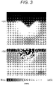
- Fig. 3 illustrates a cross-sectional optical microscope image and a Raman spectroscopic mapping image of the AlN substrate 10 subjected to the processing step S11.
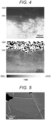
- Fig. 4 illustrates a cross-sectional optical microscope image and a Raman spectroscopic mapping image of the AlN substrate 10 subjected to the processing step S11 and the strained layer removal step S12.
- Figs. 3 and 4 respectively illustrate AlN surfaces 1000 and 1001.
- Fig. 4 illustrates that the AlN surface 1000 is etched by the strained layer removal step S12 to form the AlN surface 1001.
- mapping image here indicates mapping results of full width at half maximum (FWHM) at E 2 high peak (corresponding to up to 660 cm -1 ).
- Fig. 5 illustrates an SEM image of the AlN substrate 10 thermally etched under the heating conditions 1. According to Fig. 5 , it can be understood that formation of Al droplets associated with nitrogen desorption is suppressed on the surface of the AlN substrate 10 thermally etched under the heating conditions 1.
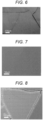
- Fig. 6 illustrates an SEM image of the AlN substrate 10 thermally etched under the heating conditions 2. According to Fig. 6 , it can be understood that formation of Al droplets is suppressed on the surface of the AlN substrate 10 thermally etched under the heating conditions 2.
- Fig. 7 illustrates an SEM image of the AlN substrate 10 thermally etched under the heating conditions 3. According to Fig. 7 , it can be understood that the formation of Al droplets is suppressed on the surface of the AlN substrate 10 thermally etched under the heating conditions 3.
- Figs. 5 , 6, 7, and 8 it can be understood that formation of Al droplets in the thermal etching of the AlN substrate 10 under the nitrogen atmosphere can be suppressed by a low heating temperature and/or a high nitrogen back pressure.
Landscapes
- Engineering & Computer Science (AREA)
- Chemical & Material Sciences (AREA)
- Physics & Mathematics (AREA)
- Optics & Photonics (AREA)
- Organic Chemistry (AREA)
- Crystallography & Structural Chemistry (AREA)
- Materials Engineering (AREA)
- Metallurgy (AREA)
- Mechanical Engineering (AREA)
- Plasma & Fusion (AREA)
- Thermal Sciences (AREA)
- Inorganic Chemistry (AREA)
- Crystals, And After-Treatments Of Crystals (AREA)
- Recrystallisation Techniques (AREA)
Applications Claiming Priority (2)
| Application Number | Priority Date | Filing Date | Title |
|---|---|---|---|
| JP2020072552 | 2020-04-14 | ||
| PCT/JP2021/013748 WO2021210395A1 (ja) | 2020-04-14 | 2021-03-30 | 窒化アルミニウム基板の製造方法、窒化アルミニウム基板、及び、レーザー加工により窒化アルミニウム基板に導入された歪層を除去する方法 |
Publications (2)
| Publication Number | Publication Date |
|---|---|
| EP4137624A1 true EP4137624A1 (de) | 2023-02-22 |
| EP4137624A4 EP4137624A4 (de) | 2024-05-22 |
Family
ID=78084948
Family Applications (1)
| Application Number | Title | Priority Date | Filing Date |
|---|---|---|---|
| EP21789083.9A Pending EP4137624A4 (de) | 2020-04-14 | 2021-03-30 | Verfahren zur herstellung eines aluminiumnitridsubstrats, aluminiumnitridsubstrat und verfahren zur entfernung einer in ein aluminiumnitridsubstrat durch laserbearbeitung eingeführten spannungsschicht |
Country Status (6)
| Country | Link |
|---|---|
| US (1) | US12325936B2 (de) |
| EP (1) | EP4137624A4 (de) |
| JP (1) | JP7748604B2 (de) |
| CN (1) | CN115398604A (de) |
| TW (1) | TWI876015B (de) |
| WO (1) | WO2021210395A1 (de) |
Family Cites Families (16)
| Publication number | Priority date | Publication date | Assignee | Title |
|---|---|---|---|---|
| JP3170005B2 (ja) * | 1991-10-29 | 2001-05-28 | 株式会社東芝 | セラミック回路基板 |
| JPH10305420A (ja) | 1997-03-04 | 1998-11-17 | Ngk Insulators Ltd | 酸化物単結晶からなる母材の加工方法、機能性デバイスの製造方法 |
| JP3408805B2 (ja) | 2000-09-13 | 2003-05-19 | 浜松ホトニクス株式会社 | 切断起点領域形成方法及び加工対象物切断方法 |
| JP2003218518A (ja) * | 2002-01-28 | 2003-07-31 | Tokuyama Corp | 回路基板の製造方法 |
| US7125801B2 (en) * | 2003-08-06 | 2006-10-24 | Matsushita Electric Industrial Co., Ltd. | Method of manufacturing Group III nitride crystal substrate, etchant used in the method, Group III nitride crystal substrate, and semiconductor device including the same |
| JP2007119273A (ja) * | 2005-10-26 | 2007-05-17 | Matsushita Electric Ind Co Ltd | 炭化珪素単結晶の成長方法 |
| US8257987B2 (en) * | 2006-02-02 | 2012-09-04 | Trustees Of Boston University | Planarization of GaN by photoresist technique using an inductively coupled plasma |
| JP2009190936A (ja) * | 2008-02-14 | 2009-08-27 | Sumitomo Electric Ind Ltd | Iii族窒化物結晶の製造方法 |
| WO2011008893A1 (en) | 2009-07-15 | 2011-01-20 | Io Semiconductor | Semiconductor-on-insulator with backside heat dissipation |
| JP2012074451A (ja) * | 2010-09-28 | 2012-04-12 | Stanley Electric Co Ltd | 配線基板及びその製造方法 |
| US8822314B2 (en) * | 2012-06-14 | 2014-09-02 | Palo Alto Research Center Incorporated | Method of growing epitaxial layers on a substrate |
| JP6355540B2 (ja) | 2014-12-04 | 2018-07-11 | 株式会社ディスコ | ウエーハの生成方法 |
| JP6238322B2 (ja) * | 2015-09-11 | 2017-11-29 | 国立大学法人三重大学 | 窒化物半導体基板の製造方法 |
| JP6833818B2 (ja) * | 2016-03-29 | 2021-02-24 | 株式会社東芝 | セラミック回路基板およびそれを用いた半導体装置 |
| JP7093656B2 (ja) * | 2018-03-22 | 2022-06-30 | レール・リキード-ソシエテ・アノニム・プール・レテュード・エ・レクスプロワタシオン・デ・プロセデ・ジョルジュ・クロード | エッチング方法および半導体素子の製造方法 |
| JP2020038955A (ja) * | 2018-09-04 | 2020-03-12 | 株式会社トクヤマ | Iii族窒化物単結晶の切断方法 |
-
2021
- 2021-03-30 TW TW110111493A patent/TWI876015B/zh active
- 2021-03-30 WO PCT/JP2021/013748 patent/WO2021210395A1/ja not_active Ceased
- 2021-03-30 EP EP21789083.9A patent/EP4137624A4/de active Pending
- 2021-03-30 JP JP2022515290A patent/JP7748604B2/ja active Active
- 2021-03-30 US US17/996,198 patent/US12325936B2/en active Active
- 2021-03-30 CN CN202180028148.4A patent/CN115398604A/zh active Pending
Also Published As
| Publication number | Publication date |
|---|---|
| WO2021210395A1 (ja) | 2021-10-21 |
| JPWO2021210395A1 (de) | 2021-10-21 |
| JP7748604B2 (ja) | 2025-10-03 |
| EP4137624A4 (de) | 2024-05-22 |
| US12325936B2 (en) | 2025-06-10 |
| CN115398604A (zh) | 2022-11-25 |
| TW202213663A (zh) | 2022-04-01 |
| TWI876015B (zh) | 2025-03-11 |
| US20230212785A1 (en) | 2023-07-06 |
Similar Documents
| Publication | Publication Date | Title |
|---|---|---|
| JP5363977B2 (ja) | 照射アニールを用いて作製されたセミコンダクタ・オン・インシュレータ構造 | |
| JP2026048816A (ja) | 大口径炭化ケイ素ウェハ | |
| EP0567129A2 (de) | Verfahren zur Bearbeitung von Diamanten | |
| KR20180125532A (ko) | 분리될 고형체의 결합된 레이저 처리 방법 | |
| US12255073B2 (en) | Silicon carbide substrate manufacturing method, silicon carbide substrate, and method of removing strain layer introduced into silicon carbide substrate by laser processing | |
| US20210047749A1 (en) | Diameter expansion of aluminum nitride crystals during growth by physical vapor transport | |
| JP2009266892A (ja) | 化合物半導体結晶基材の製造方法 | |
| US12325936B2 (en) | Aluminum nitride substrate manufacturing method, aluminum nitride substrate, and method of removing strain layer introduced into aluminum nitride substrate by laser processing | |
| US12509795B2 (en) | Method for manufacturing aluminum nitride substrate, aluminum nitride substrate, and method for forming aluminum nitride layer | |
| JP2003168646A (ja) | 半導体装置の製造方法 | |
| US12151941B2 (en) | SiC substrate and SiC ingot | |
| US12037249B2 (en) | SiC substrate and SiC ingot | |
| EP4137614A1 (de) | Verfahren zur herstellung eines aluminiumnitridsubstrats, aluminiumnitridsubstrat und verfahren zur unterdrückung des auftretens von rissen in einer aluminiumnitridschicht | |
| JP7214034B1 (ja) | SiCデバイスの製造方法 | |
| JP7214032B1 (ja) | SiCデバイスの製造方法 | |
| WO2019039533A1 (ja) | ダイヤモンド基板の製造方法 | |
| CN115443352B (en) | Method for manufacturing aluminum nitride substrate, and method for forming aluminum nitride layer | |
| EP4455375A1 (de) | Nitridhalbleitersubstrat und verfahren zur herstellung eines nitridhalbleitersubstrats | |
| JP2026513238A (ja) | 単結晶窒化アルミニウム基板およびそれから作製された光電子装置 | |
| CN120828475A (zh) | 脆性晶体的热应力分片方法 | |
| JP2018199619A (ja) | 窒化ガリウム基板 |
Legal Events
| Date | Code | Title | Description |
|---|---|---|---|
| STAA | Information on the status of an ep patent application or granted ep patent |
Free format text: STATUS: THE INTERNATIONAL PUBLICATION HAS BEEN MADE |
|
| PUAI | Public reference made under article 153(3) epc to a published international application that has entered the european phase |
Free format text: ORIGINAL CODE: 0009012 |
|
| STAA | Information on the status of an ep patent application or granted ep patent |
Free format text: STATUS: REQUEST FOR EXAMINATION WAS MADE |
|
| 17P | Request for examination filed |
Effective date: 20221108 |
|
| AK | Designated contracting states |
Kind code of ref document: A1 Designated state(s): AL AT BE BG CH CY CZ DE DK EE ES FI FR GB GR HR HU IE IS IT LI LT LU LV MC MK MT NL NO PL PT RO RS SE SI SK SM TR |
|
| DAV | Request for validation of the european patent (deleted) | ||
| DAX | Request for extension of the european patent (deleted) | ||
| A4 | Supplementary search report drawn up and despatched |
Effective date: 20240424 |
|
| RIC1 | Information provided on ipc code assigned before grant |
Ipc: B23K 26/384 20140101ALI20240418BHEP Ipc: B23K 26/082 20140101ALI20240418BHEP Ipc: C30B 29/40 20060101ALI20240418BHEP Ipc: B23K 26/402 20140101ALI20240418BHEP Ipc: H01L 21/306 20060101ALI20240418BHEP Ipc: B23K 26/382 20140101ALI20240418BHEP Ipc: C30B 33/08 20060101ALI20240418BHEP Ipc: C30B 33/02 20060101AFI20240418BHEP |