EP4135030A2 - Halbleiterpaket und verfahren zum herstellen des halbleiterpakets - Google Patents
Halbleiterpaket und verfahren zum herstellen des halbleiterpakets Download PDFInfo
- Publication number
- EP4135030A2 EP4135030A2 EP22166449.3A EP22166449A EP4135030A2 EP 4135030 A2 EP4135030 A2 EP 4135030A2 EP 22166449 A EP22166449 A EP 22166449A EP 4135030 A2 EP4135030 A2 EP 4135030A2
- Authority
- EP
- European Patent Office
- Prior art keywords
- group
- electrodes
- semiconductor chip
- bonding pads
- semiconductor
- Prior art date
- Legal status (The legal status is an assumption and is not a legal conclusion. Google has not performed a legal analysis and makes no representation as to the accuracy of the status listed.)
- Pending
Links
Images


Classifications
-
- H—ELECTRICITY
- H10—SEMICONDUCTOR DEVICES; ELECTRIC SOLID-STATE DEVICES NOT OTHERWISE PROVIDED FOR
- H10W—GENERIC PACKAGES, INTERCONNECTIONS, CONNECTORS OR OTHER CONSTRUCTIONAL DETAILS OF DEVICES COVERED BY CLASS H10
- H10W70/00—Package substrates; Interposers; Redistribution layers [RDL]
- H10W70/60—Insulating or insulated package substrates; Interposers; Redistribution layers
- H10W70/62—Insulating or insulated package substrates; Interposers; Redistribution layers characterised by their interconnections
- H10W70/65—Shapes or dispositions of interconnections
- H10W70/652—Cross-sectional shapes
- H10W70/6528—Cross-sectional shapes of the portions that connect to chips, wafers or package parts
-
- H—ELECTRICITY
- H10—SEMICONDUCTOR DEVICES; ELECTRIC SOLID-STATE DEVICES NOT OTHERWISE PROVIDED FOR
- H10W—GENERIC PACKAGES, INTERCONNECTIONS, CONNECTORS OR OTHER CONSTRUCTIONAL DETAILS OF DEVICES COVERED BY CLASS H10
- H10W90/00—Package configurations
-
- G—PHYSICS
- G11—INFORMATION STORAGE
- G11C—STATIC STORES
- G11C5/00—Details of stores covered by group G11C11/00
- G11C5/02—Disposition of storage elements, e.g. in the form of a matrix array
- G11C5/025—Geometric lay-out considerations of storage- and peripheral-blocks in a semiconductor storage device
-
- G—PHYSICS
- G11—INFORMATION STORAGE
- G11C—STATIC STORES
- G11C5/00—Details of stores covered by group G11C11/00
- G11C5/02—Disposition of storage elements, e.g. in the form of a matrix array
- G11C5/04—Supports for storage elements, e.g. memory modules; Mounting or fixing of storage elements on such supports
-
- G—PHYSICS
- G11—INFORMATION STORAGE
- G11C—STATIC STORES
- G11C5/00—Details of stores covered by group G11C11/00
- G11C5/06—Arrangements for interconnecting storage elements electrically, e.g. by wiring
- G11C5/063—Voltage and signal distribution in integrated semi-conductor memory access lines, e.g. word-line, bit-line, cross-over resistance, propagation delay
-
- H—ELECTRICITY
- H10—SEMICONDUCTOR DEVICES; ELECTRIC SOLID-STATE DEVICES NOT OTHERWISE PROVIDED FOR
- H10W—GENERIC PACKAGES, INTERCONNECTIONS, CONNECTORS OR OTHER CONSTRUCTIONAL DETAILS OF DEVICES COVERED BY CLASS H10
- H10W20/00—Interconnections in chips, wafers or substrates
- H10W20/20—Interconnections within wafers or substrates, e.g. through-silicon vias [TSV]
-
- H—ELECTRICITY
- H10—SEMICONDUCTOR DEVICES; ELECTRIC SOLID-STATE DEVICES NOT OTHERWISE PROVIDED FOR
- H10W—GENERIC PACKAGES, INTERCONNECTIONS, CONNECTORS OR OTHER CONSTRUCTIONAL DETAILS OF DEVICES COVERED BY CLASS H10
- H10W72/00—Interconnections or connectors in packages
- H10W72/20—Bump connectors, e.g. solder bumps or copper pillars; Dummy bumps; Thermal bumps
-
- H—ELECTRICITY
- H10—SEMICONDUCTOR DEVICES; ELECTRIC SOLID-STATE DEVICES NOT OTHERWISE PROVIDED FOR
- H10W—GENERIC PACKAGES, INTERCONNECTIONS, CONNECTORS OR OTHER CONSTRUCTIONAL DETAILS OF DEVICES COVERED BY CLASS H10
- H10W72/00—Interconnections or connectors in packages
- H10W72/90—Bond pads, in general
-
- H—ELECTRICITY
- H10—SEMICONDUCTOR DEVICES; ELECTRIC SOLID-STATE DEVICES NOT OTHERWISE PROVIDED FOR
- H10W—GENERIC PACKAGES, INTERCONNECTIONS, CONNECTORS OR OTHER CONSTRUCTIONAL DETAILS OF DEVICES COVERED BY CLASS H10
- H10W90/00—Package configurations
- H10W90/20—Configurations of stacked chips
- H10W90/22—Configurations of stacked chips the stacked chips being on both top and bottom sides of a package substrate, interposer or RDL
-
- G—PHYSICS
- G11—INFORMATION STORAGE
- G11C—STATIC STORES
- G11C2207/00—Indexing scheme relating to arrangements for writing information into, or reading information out from, a digital store
- G11C2207/10—Aspects relating to interfaces of memory device to external buses
- G11C2207/105—Aspects related to pads, pins or terminals
-
- G—PHYSICS
- G11—INFORMATION STORAGE
- G11C—STATIC STORES
- G11C2207/00—Indexing scheme relating to arrangements for writing information into, or reading information out from, a digital store
- G11C2207/10—Aspects relating to interfaces of memory device to external buses
- G11C2207/108—Wide data ports
-
- H—ELECTRICITY
- H10—SEMICONDUCTOR DEVICES; ELECTRIC SOLID-STATE DEVICES NOT OTHERWISE PROVIDED FOR
- H10W—GENERIC PACKAGES, INTERCONNECTIONS, CONNECTORS OR OTHER CONSTRUCTIONAL DETAILS OF DEVICES COVERED BY CLASS H10
- H10W20/00—Interconnections in chips, wafers or substrates
- H10W20/40—Interconnections external to wafers or substrates, e.g. back-end-of-line [BEOL] metallisations or vias connecting to gate electrodes
- H10W20/49—Adaptable interconnections, e.g. fuses or antifuses
- H10W20/491—Antifuses, i.e. interconnections changeable from non-conductive to conductive
-
- H—ELECTRICITY
- H10—SEMICONDUCTOR DEVICES; ELECTRIC SOLID-STATE DEVICES NOT OTHERWISE PROVIDED FOR
- H10W—GENERIC PACKAGES, INTERCONNECTIONS, CONNECTORS OR OTHER CONSTRUCTIONAL DETAILS OF DEVICES COVERED BY CLASS H10
- H10W20/00—Interconnections in chips, wafers or substrates
- H10W20/40—Interconnections external to wafers or substrates, e.g. back-end-of-line [BEOL] metallisations or vias connecting to gate electrodes
- H10W20/49—Adaptable interconnections, e.g. fuses or antifuses
- H10W20/493—Fuses, i.e. interconnections changeable from conductive to non-conductive
-
- H—ELECTRICITY
- H10—SEMICONDUCTOR DEVICES; ELECTRIC SOLID-STATE DEVICES NOT OTHERWISE PROVIDED FOR
- H10W—GENERIC PACKAGES, INTERCONNECTIONS, CONNECTORS OR OTHER CONSTRUCTIONAL DETAILS OF DEVICES COVERED BY CLASS H10
- H10W72/00—Interconnections or connectors in packages
- H10W72/01—Manufacture or treatment
- H10W72/0198—Manufacture or treatment batch processes
-
- H—ELECTRICITY
- H10—SEMICONDUCTOR DEVICES; ELECTRIC SOLID-STATE DEVICES NOT OTHERWISE PROVIDED FOR
- H10W—GENERIC PACKAGES, INTERCONNECTIONS, CONNECTORS OR OTHER CONSTRUCTIONAL DETAILS OF DEVICES COVERED BY CLASS H10
- H10W72/00—Interconnections or connectors in packages
- H10W72/071—Connecting or disconnecting
- H10W72/072—Connecting or disconnecting of bump connectors
- H10W72/07251—Connecting or disconnecting of bump connectors characterised by changes in properties of the bump connectors during connecting
- H10W72/07254—Connecting or disconnecting of bump connectors characterised by changes in properties of the bump connectors during connecting changes in dispositions
-
- H—ELECTRICITY
- H10—SEMICONDUCTOR DEVICES; ELECTRIC SOLID-STATE DEVICES NOT OTHERWISE PROVIDED FOR
- H10W—GENERIC PACKAGES, INTERCONNECTIONS, CONNECTORS OR OTHER CONSTRUCTIONAL DETAILS OF DEVICES COVERED BY CLASS H10
- H10W72/00—Interconnections or connectors in packages
- H10W72/071—Connecting or disconnecting
- H10W72/073—Connecting or disconnecting of die-attach connectors
-
- H—ELECTRICITY
- H10—SEMICONDUCTOR DEVICES; ELECTRIC SOLID-STATE DEVICES NOT OTHERWISE PROVIDED FOR
- H10W—GENERIC PACKAGES, INTERCONNECTIONS, CONNECTORS OR OTHER CONSTRUCTIONAL DETAILS OF DEVICES COVERED BY CLASS H10
- H10W72/00—Interconnections or connectors in packages
- H10W72/20—Bump connectors, e.g. solder bumps or copper pillars; Dummy bumps; Thermal bumps
- H10W72/221—Structures or relative sizes
- H10W72/227—Multiple bumps having different sizes
-
- H—ELECTRICITY
- H10—SEMICONDUCTOR DEVICES; ELECTRIC SOLID-STATE DEVICES NOT OTHERWISE PROVIDED FOR
- H10W—GENERIC PACKAGES, INTERCONNECTIONS, CONNECTORS OR OTHER CONSTRUCTIONAL DETAILS OF DEVICES COVERED BY CLASS H10
- H10W72/00—Interconnections or connectors in packages
- H10W72/20—Bump connectors, e.g. solder bumps or copper pillars; Dummy bumps; Thermal bumps
- H10W72/241—Dispositions, e.g. layouts
- H10W72/247—Dispositions of multiple bumps
- H10W72/248—Top-view layouts, e.g. mirror arrays
-
- H—ELECTRICITY
- H10—SEMICONDUCTOR DEVICES; ELECTRIC SOLID-STATE DEVICES NOT OTHERWISE PROVIDED FOR
- H10W—GENERIC PACKAGES, INTERCONNECTIONS, CONNECTORS OR OTHER CONSTRUCTIONAL DETAILS OF DEVICES COVERED BY CLASS H10
- H10W72/00—Interconnections or connectors in packages
- H10W72/20—Bump connectors, e.g. solder bumps or copper pillars; Dummy bumps; Thermal bumps
- H10W72/251—Materials
- H10W72/252—Materials comprising solid metals or solid metalloids, e.g. PbSn, Ag or Cu
-
- H—ELECTRICITY
- H10—SEMICONDUCTOR DEVICES; ELECTRIC SOLID-STATE DEVICES NOT OTHERWISE PROVIDED FOR
- H10W—GENERIC PACKAGES, INTERCONNECTIONS, CONNECTORS OR OTHER CONSTRUCTIONAL DETAILS OF DEVICES COVERED BY CLASS H10
- H10W72/00—Interconnections or connectors in packages
- H10W72/20—Bump connectors, e.g. solder bumps or copper pillars; Dummy bumps; Thermal bumps
- H10W72/29—Bond pads specially adapted therefor
-
- H—ELECTRICITY
- H10—SEMICONDUCTOR DEVICES; ELECTRIC SOLID-STATE DEVICES NOT OTHERWISE PROVIDED FOR
- H10W—GENERIC PACKAGES, INTERCONNECTIONS, CONNECTORS OR OTHER CONSTRUCTIONAL DETAILS OF DEVICES COVERED BY CLASS H10
- H10W72/00—Interconnections or connectors in packages
- H10W72/90—Bond pads, in general
- H10W72/941—Dispositions of bond pads
- H10W72/942—Dispositions of bond pads relative to underlying supporting features, e.g. bond pads, RDLs or vias
-
- H—ELECTRICITY
- H10—SEMICONDUCTOR DEVICES; ELECTRIC SOLID-STATE DEVICES NOT OTHERWISE PROVIDED FOR
- H10W—GENERIC PACKAGES, INTERCONNECTIONS, CONNECTORS OR OTHER CONSTRUCTIONAL DETAILS OF DEVICES COVERED BY CLASS H10
- H10W72/00—Interconnections or connectors in packages
- H10W72/90—Bond pads, in general
- H10W72/941—Dispositions of bond pads
- H10W72/944—Dispositions of multiple bond pads
-
- H—ELECTRICITY
- H10—SEMICONDUCTOR DEVICES; ELECTRIC SOLID-STATE DEVICES NOT OTHERWISE PROVIDED FOR
- H10W—GENERIC PACKAGES, INTERCONNECTIONS, CONNECTORS OR OTHER CONSTRUCTIONAL DETAILS OF DEVICES COVERED BY CLASS H10
- H10W74/00—Encapsulations, e.g. protective coatings
- H10W74/10—Encapsulations, e.g. protective coatings characterised by their shape or disposition
- H10W74/15—Encapsulations, e.g. protective coatings characterised by their shape or disposition on active surfaces of flip-chip devices, e.g. underfills
-
- H—ELECTRICITY
- H10—SEMICONDUCTOR DEVICES; ELECTRIC SOLID-STATE DEVICES NOT OTHERWISE PROVIDED FOR
- H10W—GENERIC PACKAGES, INTERCONNECTIONS, CONNECTORS OR OTHER CONSTRUCTIONAL DETAILS OF DEVICES COVERED BY CLASS H10
- H10W90/00—Package configurations
- H10W90/20—Configurations of stacked chips
- H10W90/24—Configurations of stacked chips at least one of the stacked chips being laterally offset from a neighbouring stacked chip, e.g. chip stacks having a staircase shape
-
- H—ELECTRICITY
- H10—SEMICONDUCTOR DEVICES; ELECTRIC SOLID-STATE DEVICES NOT OTHERWISE PROVIDED FOR
- H10W—GENERIC PACKAGES, INTERCONNECTIONS, CONNECTORS OR OTHER CONSTRUCTIONAL DETAILS OF DEVICES COVERED BY CLASS H10
- H10W90/00—Package configurations
- H10W90/20—Configurations of stacked chips
- H10W90/26—Configurations of stacked chips the stacked chips being of the same size without any chips being laterally offset, e.g. chip stacks having a rectangular shape
-
- H—ELECTRICITY
- H10—SEMICONDUCTOR DEVICES; ELECTRIC SOLID-STATE DEVICES NOT OTHERWISE PROVIDED FOR
- H10W—GENERIC PACKAGES, INTERCONNECTIONS, CONNECTORS OR OTHER CONSTRUCTIONAL DETAILS OF DEVICES COVERED BY CLASS H10
- H10W90/00—Package configurations
- H10W90/20—Configurations of stacked chips
- H10W90/291—Configurations of stacked chips characterised by containers, encapsulations, or other housings for the stacked chips
-
- H—ELECTRICITY
- H10—SEMICONDUCTOR DEVICES; ELECTRIC SOLID-STATE DEVICES NOT OTHERWISE PROVIDED FOR
- H10W—GENERIC PACKAGES, INTERCONNECTIONS, CONNECTORS OR OTHER CONSTRUCTIONAL DETAILS OF DEVICES COVERED BY CLASS H10
- H10W90/00—Package configurations
- H10W90/20—Configurations of stacked chips
- H10W90/297—Configurations of stacked chips characterised by the through-semiconductor vias [TSVs] in the stacked chips
-
- H—ELECTRICITY
- H10—SEMICONDUCTOR DEVICES; ELECTRIC SOLID-STATE DEVICES NOT OTHERWISE PROVIDED FOR
- H10W—GENERIC PACKAGES, INTERCONNECTIONS, CONNECTORS OR OTHER CONSTRUCTIONAL DETAILS OF DEVICES COVERED BY CLASS H10
- H10W90/00—Package configurations
- H10W90/701—Package configurations characterised by the relative positions of pads or connectors relative to package parts
- H10W90/721—Package configurations characterised by the relative positions of pads or connectors relative to package parts of bump connectors
- H10W90/722—Package configurations characterised by the relative positions of pads or connectors relative to package parts of bump connectors between stacked chips
-
- H—ELECTRICITY
- H10—SEMICONDUCTOR DEVICES; ELECTRIC SOLID-STATE DEVICES NOT OTHERWISE PROVIDED FOR
- H10W—GENERIC PACKAGES, INTERCONNECTIONS, CONNECTORS OR OTHER CONSTRUCTIONAL DETAILS OF DEVICES COVERED BY CLASS H10
- H10W90/00—Package configurations
- H10W90/701—Package configurations characterised by the relative positions of pads or connectors relative to package parts
- H10W90/721—Package configurations characterised by the relative positions of pads or connectors relative to package parts of bump connectors
- H10W90/724—Package configurations characterised by the relative positions of pads or connectors relative to package parts of bump connectors between a chip and a stacked insulating package substrate, interposer or RDL
-
- H—ELECTRICITY
- H10—SEMICONDUCTOR DEVICES; ELECTRIC SOLID-STATE DEVICES NOT OTHERWISE PROVIDED FOR
- H10W—GENERIC PACKAGES, INTERCONNECTIONS, CONNECTORS OR OTHER CONSTRUCTIONAL DETAILS OF DEVICES COVERED BY CLASS H10
- H10W90/00—Package configurations
- H10W90/701—Package configurations characterised by the relative positions of pads or connectors relative to package parts
- H10W90/731—Package configurations characterised by the relative positions of pads or connectors relative to package parts of die-attach connectors
- H10W90/732—Package configurations characterised by the relative positions of pads or connectors relative to package parts of die-attach connectors between stacked chips
-
- H—ELECTRICITY
- H10—SEMICONDUCTOR DEVICES; ELECTRIC SOLID-STATE DEVICES NOT OTHERWISE PROVIDED FOR
- H10W—GENERIC PACKAGES, INTERCONNECTIONS, CONNECTORS OR OTHER CONSTRUCTIONAL DETAILS OF DEVICES COVERED BY CLASS H10
- H10W90/00—Package configurations
- H10W90/701—Package configurations characterised by the relative positions of pads or connectors relative to package parts
- H10W90/731—Package configurations characterised by the relative positions of pads or connectors relative to package parts of die-attach connectors
- H10W90/734—Package configurations characterised by the relative positions of pads or connectors relative to package parts of die-attach connectors between a chip and a stacked insulating package substrate, interposer or RDL
Definitions
- Some example embodiments relate to a semiconductor package and/or a method of manufacturing the semiconductor package. More particularly, some example embodiments relate to a semiconductor package including semiconductor chips stacked using through silicon vias and/or a method of manufacturing the same.
- a high bandwidth memory (HBM) device may include vertically stacked memory dies (chips).
- the memory dies may be electrically connected to each other by through electrodes such as through silicon vias (TSVs).
- TSVs through silicon vias
- I/O data input/output
- the number of input/output through silicon vias may be an important factor to increase the number of I/O channels, but it may be difficult to reduce pitches of the through silicon vias due to a space occupied by an I/O driver circuit.
- Some example embodiments provide a semiconductor package having an improved input/output interface.
- Some example embodiments provide a method of manufacturing the semiconductor package.
- a semiconductor package includes a semiconductor package including first, second, third and fourth semiconductor chips sequentially stacked on one another.
- Each of the first, second, third and fourth semiconductor chips includes a first group of bonding pads and a second group of bonding pads alternately arranged in a first direction and input/output (I/O) circuitry selectively connected to the first group of bonding pads respectively.
- Each of the first, second and third semiconductor chips includes a first group of through electrodes electrically connected to the first group of bonding pads and a second group of through electrodes electrically connected to the second group of bonding pads.
- a semiconductor package includes first, second, third and fourth semiconductor chips sequentially stacked on one another.
- Each of the first, second and third semiconductor chips includes a first group of through electrodes and a second group of through electrodes alternately arranged in a first direction and input/output (I/O) circuitry selectively connected to the first group of through electrodes respectively.
- the first group of through electrodes of the first and third semiconductor chips are electrically connected to the second group of through electrodes of the second and fourth semiconductor chips respectively, and the second group of through electrodes of the first and third semiconductor chips are electrically connected to the first group of through electrodes of the first and third semiconductor chips respectively.
- a semiconductor package includes first, second, third and fourth semiconductor chips sequentially stacked on one another and electrically connected to each other by conductive connection members.
- Each of the first, second, third and fourth semiconductor chips includes a first surface and a second surface opposite to each other, a first group of bonding pads and a second group of bonding pads on the first surface alternately arranged in a first direction, and input/output (I/O) circuitry selectively connected to the first group of bonding pads respectively.
- Each of the first, second and third semiconductor chips further includes a first group of through electrodes electrically connected to the first group of bonding pads and a second group of through electrodes electrically connected to the second group of bonding pads stacked on the package substrate.
- the first group of bonding pads of the first and third semiconductor chips are electrically connected to the second group of bonding pads of the second and fourth semiconductor chips respectively, and the second group of bonding pads of the first and third semiconductor chips are electrically connected to the first group of the second and fourth semiconductor chips respectively.
- a semiconductor package may include first, second, third and fourth semiconductor chips sequentially stacked on one another.
- Each of the first, second and third semiconductor chips may include a first group of through electrodes and a second group of through electrodes alternately arranged in a first direction.
- the first group of through electrodes may be selectively connected to I/O circuitry of each semiconductor chip respectively.
- the second group of through electrodes may not be connected to the I/O circuitry.
- the semiconductor package may provide an input/output (TSV I/O) structure having a larger number of through silicon vias to thereby implement a broadband interface.
- TSV I/O input/output
- FIGS. 1 to 25 represent non-limiting, example embodiments as described herein.
- Elements and/or properties thereof that are “substantially identical” to, “substantially the same” as or “substantially equal” to other elements and/or properties thereof will be understood to include elements and/or properties thereof that are identical to, the same as, or equal to the other elements and/or properties thereof within manufacturing tolerances and/or material tolerances.
- Elements and/or properties thereof that are identical or substantially identical to and/or the same or substantially the same as other elements and/or properties thereof may be structurally the same or substantially the same, functionally the same or substantially the same, and/or compositionally the same or substantially the same.
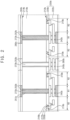
- FIG. 1 is a cross-sectional view illustrating a semiconductor package in accordance with some example embodiments.
- FIG. 2 is an enlarged cross-sectional view illustrating portion 'A' in FIG. 1 .
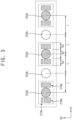
- FIG. 3 is a cross-sectional view taken along the line I-I' in FIG. 1 .
- a semiconductor package 10 may include stacked semiconductor chips.
- the semiconductor package 10 may include a base chip 100, first to fourth semiconductor chips 200a, 200b, 200c and/or 200d sequentially stacked on the base chip 100, and/or a molding member 300 on the base chip 100 covering the first to fourth semiconductor chips 200a, 200b, 200c and/or 200d.
- the semiconductor package 10 may further include first to fourth conductive connection members 280a, 280b, 280c and/or 280d for electrical connection between the base chip 100 and the first to fourth semiconductor chips 200a, 200b, 200c and/or 200d.
- the first to fourth semiconductor chips 200a, 200b, 200c, and/or 200d may be substantially the same as or similar to each other.
- same or like reference numerals will be used to refer to the same or like elements and any further repetitive explanation concerning the above elements will be omitted.
- the base chip 100 and the first to fourth semiconductor chips 200a, 200b, 200c and/or 200d may be stacked on a package substrate such as printed circuit board (PCB), an interposer, etc.
- a package substrate such as printed circuit board (PCB), an interposer, etc.
- the semiconductor package as multi-chip package including five stacked semiconductor dies (chips) 100, 200a, 200b, 200c and 200d are exemplarily illustrated, and thus, it may not be limited thereto.
- the semiconductor package 10 may include a high bandwidth memory (HBM) device.
- the high bandwidth memory (HBM) package may have a wideband interface for faster data exchange than a processor chip.
- the HBM package may have an input/output (TSV I/O) structure having a large number of through silicon vias (TSVs) to implement the wideband interface.
- the processor chip that requires support for the HBM package may be central processing unit (CPU), graphics processing unit (GPU), microprocessor, microcontroller, or application processor (AP), an application specific integrated circuit (ASIC) chip including a digital signal processing core and an interface for signal exchange, etc.
- CPU central processing unit
- GPU graphics processing unit
- AP application processor
- ASIC application specific integrated circuit
- the semiconductor package 10 may include the base chip 100 as a buffer die and the first to fourth semiconductor chips 200a, 200b, 200c and/or 200d as memory dies, which are sequentially stacked on one another.
- the first to fourth semiconductor chips 200a, 200b, 200c and/or 200d may be electrically connected to each other by through electrodes such as through silicon vias (TSVs).
- TSVs through silicon vias
- the memory die may include a memory device
- the buffer die may include a controller for controlling the memory device.
- the base chip 100 may have an upper surface 102 and a lower surface 104 opposite to each other.
- Substrate pads 110 for electrical connection with the first semiconductor chip 200a may be provided on the upper surface 102 of the base chip 100.
- Outer connection pads 400 for electrical connection with an external device may be provided on the lower surface 104 of the base substrate 100.
- the first semiconductor chip 200a may include a first substrate 210a, a first front insulation layer 230a, a plurality of first bonding pads 240a, a plurality of first through electrodes 250a and/or a plurality of second bonding pads 270a. Additionally, the first semiconductor chip 200a may further include first conductive connection members 280a provided on the first bonding pads 240a respectively. The first semiconductor chip 200a may be mounted on the base chip 100 via the first conductive connection members 280a.
- the first conductive connection members 280a may include conductive bumps such as solder bumps.
- the first substrate 210a may have a first surface 212a and a second surface 214a opposite to each other.
- the first surface may be an active surface, and the second surface may be a non-active surface.
- Circuit patterns and/or cells may be formed in the first surface 212a of the first substrate 210a.
- the first substrate 210a may be a single crystalline silicon substrate.
- the circuit patterns may include a transistor, a capacitor, a diode, etc.
- the circuit patterns may constitute circuit elements.
- the first semiconductor chip 200a may be a semiconductor device including a plurality of the circuit elements formed therein.
- the first front insulation layer 230a may be provided as an insulation interlayer on the first surface 212a, e.g., the active surface of the first substrate 210a.
- the first front insulation layer 230a may include a plurality of insulation layers and wirings in the insulation layers.
- the first bonding pads 240a may be provided in the outermost insulation layer of the first front insulation layer 230a.
- the first through electrodes 250a may be provided to penetrate through the first substrate 210a from the first surface 212a to the second surface 214a of the first substrate 210a. A first end portion of the first through electrodes 250a may contact the wiring of the first front insulation layer. However, it may not be limited thereto, and for example, the first through electrodes 250a may be provided to penetrate through the first front insulation layer and directly contact the first bonding pad 240a.
- a first backside insulation layer 260a (shown in FIG. 8 ) may be provided on the second surface 214a, e.g., the backside surface of the first substrate 210a.
- the second bonding pads 270a may be provided in the first backside insulation layer 260a.
- the second bonding pad 270a may be arranged on an exposed surface of the first through electrodes 250a. Accordingly, the first and second bonding pads 240a and 270a may be electrically connected to each other by the first through electrodes 250a.
- the first and second bonding pads 240a and 270a may be arranged in respective pad arrays on an upper surface and a lower surface of the first semiconductor chip, and the first through electrodes 250a may be provided in the first surface 210a to be arranged in an array.
- the via array of the first through electrodes 250a may be designed to correspond to the pad arrays of the first and second bonding pads 240a and 270a.
- the first through electrodes 250a may include a first group of through electrodes 252a and/or a second group of through electrodes 253a alternately arranged in a first direction.
- the first group of through electrodes 252a may be arranged to be spaced apart from each other in the first direction.
- the second group of through electrodes 253a may be arranged to be spaced apart from each other in the first direction.
- Each, or one or more, of the second group of through electrodes 253a may be arranged between the first group of through electrodes 252a adjacent to each other.
- the first through electrodes 250a may be arranged to be spaced apart from each other by the same distance in the first direction.
- the first bonding pads 240a may include a first group of bonding pads 242a electrically connected to the first group of through electrodes 252a respectively and/or a second group of bonding pads 243a electrically connected to the second group of through electrodes 253a respectively.
- the first group of bonding pads 242a and the second group of bonding pads 243a may be alternately arranged in the first direction.
- the second bonding pads 270a may include a first group of bonding pads 272a electrically connected to the first group of through electrodes 252a respectively and/or a second group of bonding pads 273a electrically connected to the second group of through electrodes 253a respectively.
- the first group of bonding pads 272a and the second group of bonding pads 273a may be alternately arranged in the first direction.
- Each, or one or more, of the first group of through electrodes 252a and/or the second group of through electrodes 253a may be used as a portion of an input/output (I/O) path through which data signals are transmitted.
- the first and/or second bonding pads 240a and 270a electrically connected to each other by the first group of through electrodes 252a and/or the second group of through electrodes 253a, respectively, may be used as data input/output (I/O) pads.
- the first group of through electrodes 252a and/or the first group of bonding pads 242a and/or 272a may be selectively connected to an I/O circuitry 218a.
- the second group of through electrodes 253a and/or the second group of bonding pads 243a and/or 273a may not be connected to the I/O circuitry.
- the first semiconductor chip 200a may further include a fuse portion 215a (shown in FIG. 9 ) capable of electrically decoupling the I/O circuitry 218a from the first group of through electrodes 252a and the first group of bonding pads 242a and 272a.
- the fuse portion may include a programmable fuse or an anti-fuse. Accordingly, the I/O circuitry 218a may be selectively connected to or disconnected from the first group of through electrodes 252a and/or the first group of connection pads 242a and/or 272a by the fuse portion.
- the second semiconductor chip 200b may include a second substrate 210b, a second front insulation layer 230b, a plurality of third bonding pads 240b, a plurality of second through electrodes 250b and/or a plurality of fourth bonding pads 270b. Additionally, the second semiconductor chip 200b may further include second conductive connection members 280b provided on the third bonding pads 240b respectively. The second semiconductor chip 200b may be mounted on the first semiconductor chip 200b via the second conductive connection members 280b.
- the second conductive connection members 280b may include conductive bumps such as solder bumps.
- the second through electrodes 250b may include a first group of through electrodes 252b and/or a second group of through electrodes 253b alternately arranged in a first direction D1.
- the first group of through electrodes 252b may be arranged to be spaced apart from each other in the first direction D1.
- the second group of through electrodes 253b may be arranged to be spaced apart from each other in the first direction D1.
- Each, or one or more, of the second group of through electrodes 253b may be arranged between the first group of through electrodes 252b adjacent to each other.
- a distance (between midpoints) 2L between the adjacent first through electrodes 252ba of the first group may be equal to a distance 2L between the adjacent through electrodes 253b of the second group.
- a distance L between the through electrode 252b of the first group and the through electrode 253b of the second group adjacent to each other may be half of the distance 2L between the adjacent through electrodes 252b of the first group.
- the third bonding pads 240b may include a first group of bonding pads 242b electrically connected to the first group of through electrodes 252b respectively and/or a second group of bonding pads 243b electrically connected to the second group of through electrodes 253b respectively.
- the first group of bonding pads 242b and the second group of bonding pads 243b may be alternately arranged in the first direction D1.
- the fourth bonding pads 270b may include a first group of bonding pads 272b electrically connected to the first group of through electrodes 252b respectively and/or a second group of bonding pads 273b electrically connected to the second group of through electrodes 253b respectively.
- the first group of bonding pads 272b and the second group of bonding pads 273b may be alternately arranged in the first direction D1.
- circuit patterns 216b may include an input/output (I/O) circuitry 218b for transmitting data signals and/or an electrostatic discharge circuitry 219b associated with the I/O circuitry 218b.
- I/O input/output
- Each, or one or more, of the first group of through electrodes 252b and/or the second group of through electrodes 253b may be used as a portion of an input/output (I/O) path through which the data signals are transmitted.
- the third and fourth bonding pads 240b and 270b may be electrically connected to each other by the first group of through electrodes 252b and the second group of through electrodes 253b, respectively, may be used as input/output (I/O) pads.
- the second semiconductor chip may further include control signal through electrodes for transmitting control signals such as address and command, and/or control signal pads electrically connected to the control signal through electrodes.
- the first group of through electrodes 252b and/or the first group of bonding pads 242b and 272b may be selectively connected to the I/O circuitry 218b.
- the second group of through electrodes 253b and/or the second group of bonding pads 243b and/or 273b may not be connected to the I/O circuitry.
- the circuit pattern 216b may further include a fuse portion 215b capable of electrically decoupling the I/O circuitry 218b from the first group of through electrodes 252b and/or the first group of bonding pads 242b and/or 272b.
- the fuse portion may include a programmable fuse and/or an anti-fuse. Accordingly, the I/O circuitry 218b may be selectively connected to or disconnected from the first group of through electrodes 252b and/or the first group of connection pads 242b and/or 272b by the fuse portion.
- a second region R2 in which the I/O circuitry 218b and/or the electrostatic discharge circuitry 219b are formed may be provided around a first region R1 in which the first group of through electrodes 252b are formed.
- the first region R1 may be a TSV region
- the second region R2 may be an I/O circuit region. Since the second group of through electrodes 253b is not connected to the I/O circuitry, an additional I/O circuit region may not be provided around the region in which the second group of through electrodes 253b is formed.
- the second group of through electrodes 253b may be arranged between the first group of through electrodes 252b while maintaining the original array of the first group of through electrodes 252b.
- TSV I/O input/output
- the second semiconductor chip 200b may be identical to the first semiconductor chip 200a in terms of structural form.
- an arrangement of through electrodes and an arrangement of bonding pads of the second semiconductor chip 200b may be the same as the arrangement of the through electrodes and the arrangement of the bonding pads of the first semiconductor chip 200a.
- the second semiconductor chip 200b may be stacked on the first semiconductor chip 200a through the second conductive connection members 280b.
- the second semiconductor chip 200b may be arranged on the first semiconductor chip 200a such that the third bonding pad 240b of the second semiconductor chip 200b faces the second bonding pad 270a of the first semiconductor chip 200a.
- the second semiconductor chip 200b may be offset from the first semiconductor chip 200a by a preset (or alternately given) interval (-P) in the first direction such that the first group of through electrodes 252b of the second semiconductor chip 200b are electrically connected to the second group of through electrodes 253a of the first semiconductor chip 200a, respectively, and the second group of through electrodes 253b of the second semiconductor chip 200b are electrically connected to the first group of through electrodes 252a of the first semiconductor chip 200a, respectively.
- the preset (or alternately given) interval may be a distance between adjacent through electrodes, for example, a pitch.
- the first group of bonding pads 242b of the third bonding pads 240b of the second semiconductor chip 200b may be electrically connected to the second group of bonding pads 273a of the second bonding pads 270a of the first semiconductor chip 200a, respectively, and the second group of bonding pads 243b of the third bonding pads 240b of the second semiconductor chip 200b may be electrically connected to the first group of bonding pads 272a of the second bonding pads 270a of the first semiconductor chip 200a, respectively.
- the third semiconductor chip 200c may include a third substrate 210c, a third front insulation layer 230c, a plurality of fifth bonding pads 240c, a plurality of third through electrodes 250c and/or a plurality of sixth bonding pads 270c. Additionally, the third semiconductor chip 200c may further include third conductive connection members 280c provided on the fifth bonding pads 240c respectively. The third semiconductor chip 200c may be mounted on the second semiconductor chip 200b via the third conductive connection members 280c.
- the third conductive connection members 280c may include conductive bumps such as solder bumps.
- the third through electrodes 250c may include a first group of through electrodes 252c and/or a second group of through electrodes 253c alternately arranged in a first direction.
- the first group of through electrodes 252c may be arranged to be spaced apart from each other in the first direction.
- the second group of through electrodes 253c may be arranged to be spaced apart from each other in the first direction.
- Each, or one or more, of the second group of through electrodes 253c may be arranged between the first group of through electrodes 252c adjacent to each other.
- the fifth bonding pads 240c may include a first group of bonding pads 242c electrically connected to the first group of through electrodes 252c respectively and/or a second group of bonding pads 243c electrically connected to the second group of through electrodes 253c respectively.
- the first group of bonding pads 242c and the second group of bonding pads 243c may be alternately arranged in the first direction.
- the sixth bonding pads 270c may include a first group of bonding pads 272c electrically connected to the first group of through electrodes 252c respectively and/or a second group of bonding pads 273c electrically connected to the second group of through electrodes 253c respectively.
- the first group of bonding pads 272c and the second group of bonding pads 273c may be alternately arranged in the first direction.
- Each, or one or more, of the first group of through electrodes 252c and/or the second group of through electrodes 253c may be used as a portion of an input/output (I/O) path through which data signals are transmitted.
- the first and second bonding pads 240c and 270c electrically connected to each other by the first group of through electrodes 252c and the second group of through electrodes 253c, respectively, may be used as input/output (I/O) pads.
- the first group of through electrodes 252c and/or the first group of bonding pads 242c and 272c may be selectively connected to an I/O circuitry 218c.
- the second group of through electrodes 253c and/or the second group of bonding pads 243c and 273c may not be connected to the I/O circuitry.
- the third semiconductor chip 200c may further include a fuse portion capable of electrically decoupling the I/O circuitry from the first group of through electrodes 252c and the first group of bonding pads 242c and 272c.
- the fuse portion may include a programmable fuse or an anti-fuse. Accordingly, the I/O circuitry 218c may be selectively connected to or disconnected from the first group of through electrodes 252c and the first group of connection pads 242c and 272c by the fuse portion.
- the third semiconductor chip 200c may be identical to the second semiconductor chip 200b in terms of structural form.
- an arrangement of through electrodes and an arrangement of bonding pads of the third semiconductor chip 200c may be the same as the arrangement of the through electrodes and the arrangement of the bonding pads of the second semiconductor chip 200b.
- the third semiconductor chip 200c may be stacked on the second semiconductor chip 200b through the third conductive connection members 280c.
- the third semiconductor chip 200c may be arranged on the second semiconductor chip 200b such that the fifth bonding pad 240c of the third semiconductor chip 200c faces the fourth bonding pad 270b of the second semiconductor chip 200b.
- the third semiconductor chip 200c may be offset from the second semiconductor chip 200b by a preset (or alternately given) interval (+P) in a reverse direction of the first direction such that the first group of through electrodes 252c of the third semiconductor chip 200c are electrically connected to the second group of through electrodes 253b of the second semiconductor chip 200b, respectively, and the second group of through electrodes 253c of the third semiconductor chip 200c are electrically connected to the first group of through electrodes 252b of the second semiconductor chip 200b, respectively.
- the preset (or alternately given) interval may be a distance between adjacent through electrodes, for example, a pitch.
- the first group of bonding pads 242c of the fifth bonding pads 240c of the third semiconductor chip 200c may be electrically connected to the second group of bonding pads 273b of the fourth bonding pads 270b of the second semiconductor chip 200b, respectively, and the second group of bonding pads 243c of the fifth bonding pads 240c of the third semiconductor chip 200c may be electrically connected to the first group of bonding pads 272b of the fourth bonding pads 270b of the second semiconductor chip 200b, respectively.
- the fourth semiconductor chip 200d may include a fourth substrate 210d, a fourth front insulation layer 230d and/or a plurality of seventh bonding pads 240d. Additionally, the fourth semiconductor chip 200d may further include fourth conductive connection members 280d provided on the seventh bonding pads 240d respectively. The fourth semiconductor chip 200d may be mounted on the third semiconductor chip 200c via the fourth conductive connection members 280d.
- the fourth conductive connection members 280d may include conductive bumps such as solder bumps.
- the seventh bonding pads 240d may include a first group of bonding pads 242d and/or a second group of bonding pads 243d.
- the first group of bonding pads 242d and the second group of bonding pads 243d may be alternately arranged in the first direction.
- the seventh bonding pads 240d may be used as data input/output (I/O) pads.
- the first group of bonding pads 242d may be selectively connected to an I/O circuitry 218d.
- the second group of bonding pads 243d may not be connected to the I/O circuitry.
- the fourth semiconductor chip 200d may further include a fuse portion capable of electrically decoupling the I/O circuitry 218d from the first group of bonding pads 242d.
- the fuse portion may include a programmable fuse or an anti-fuse. Accordingly, the I/O circuitry 218d may be selectively connected to or disconnected from the first group of connection pads 242d by the fuse portion.
- the fourth semiconductor chip 200d may be identical to the third semiconductor chip 200c in terms of structural form.
- an arrangement of the data input/output bonding pads of the fourth semiconductor chip 200d may be the same as the arrangement of the data input/output bonding pads of the third semiconductor chip 200c.
- the fourth semiconductor chip 200d may be stacked on the third semiconductor chip 200c through the fourth conductive connection members 280d.
- the fourth semiconductor chip 200d may be arranged on the third semiconductor chip 200c such that the seventh bonding pad 240d of the fourth semiconductor chip 200d faces the sixth bonding pad 270c of the third semiconductor chip 200c.
- the fourth semiconductor chip 200d may be offset from the third semiconductor chip 200c by a preset (or alternately given) interval (-P) in the first direction such that the first group of bonding pads 242d of the seventh bonding pads 240d of the fourth semiconductor chip 200d are electrically connected to the second group of bonding pads 273c of the sixth bonding pads 270c of the third semiconductor chip 200c, respectively, and the second group of bonding pads 243d of the seventh bonding pads 240d of the fourth semiconductor chip 200d are electrically connected to the first group of bonding pads 272c of the sixth bonding pads 270c of the third semiconductor chip 200c, respectively.
- the preset (or alternately given) interval may be a distance between adjacent through electrodes, for example, a pitch.
- each, or one or more, of the first, second and/or third through electrodes 250a, 250b, and 250c may have a first diameter.
- the first diameter may be within a range of 3 ⁇ m to 20 ⁇ m.
- Each, or one or more, of the first to seventh bonding pads may have a second diameter greater than the first diameter.
- the second diameter may be within a range of 10 ⁇ m to 25 ⁇ m.
- the molding member 300 may be provided on the base chip 100 to cover the first, second, third and/or fourth semiconductor chips 200a, 200b, 200c and 200d.
- the molding member 300 may cover side surfaces of the first, second, third and/or fourth semiconductor chips 200a, 200b, 200c and 200d.
- the molding member 300 may cover or expose an upper surface of the fourth semiconductor chip 200d.
- the molding member 300 may include a thermosetting resin such as epoxy molding compound (EMC) material.
- the semiconductor package 10 may further include external connection members 400 respectively disposed on the outer connection pads for electrical connection with an external device provided on the lower surface 104 of the base chip 100.
- the external connection members may include solder bumps, solder balls, etc.
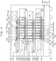
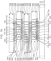
- FIG. 4 is a cross-sectional view illustrating transmission paths of data input/output (I/O) signals in the semiconductor package of FIG. 1 .
- the base chip 100 may access any of the second, third and/or fourth semiconductor chips 200b, 200c and 200d of the stack package 10 by way of at least some of the first to third through electrodes 250a, 250b and 250c, and/or data input/output signals from the second, third and/or fourth semiconductor chips 200b, 200c and 200d may be transmitted to the base chip 100 by way of at least some of the first to third through electrodes 250a, 250b and 250c.
- a signal from the I/O circuitry 218d of the fourth semiconductor chip 200d may be transmitted to the base chip 100 through the second group of through electrodes 253c of the third semiconductor chip 200c, the first group of through electrodes 252b of the second semiconductor chip 200b and the second group of through electrodes 253a of the first semiconductor chip 200a.
- the second group of through electrodes 253c of the third semiconductor chip 200c, the first group of through electrodes 252b of the second semiconductor chip 200b and the second group of through electrodes 253a of the first semiconductor chip 200a may serve as an I/O signal path P1 which connects between the I/O circuitry 218d of the fourth semiconductor chip 200d and the base chip 100.
- a signal from the I/O circuitry 218c of the third semiconductor chip 200c may be transmitted to the base chip 100 through the second group of through electrodes 253b of the second semiconductor chip 200b and the first group of through electrodes 252a of the first semiconductor chip 200a.
- the second group of through electrodes 253b of the second semiconductor chip 200b and the first group of through electrodes 252a of the first semiconductor chip 200a may serve as an I/O signal path P2 which connects between the I/O circuitry 218c of the third semiconductor chip 200c and the base chip 100.
- a signal from the I/O circuitry 218b of the second semiconductor chip 200b may be transmitted to the base chip 100 through the second group of through electrodes 253a of the first semiconductor chip 200a.
- the second group of through electrodes 253a of the first semiconductor chip 200a may serve as an I/O signal path P3 which connects between the I/O circuitry 218b of the second semiconductor chip 200b and the base chip 100.
- Only one of every four bonding pads consecutively arranged in a given row may be operated to be connected to the I/O circuitry, defining a staggered I/O circuit pattern. This may allow for point-to-point connections between the base chip 100 and the first to fourth semiconductor chips 200a, 200b, 200c and 200d.
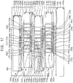
- FIG. 5 is a cross-sectional view illustrating transmission paths of data input/output (I/O) signals in a semiconductor package according to a comparative embodiment.
- a base chip 500 may access any one of the second, third and fourth semiconductor chips 600b, 600c and 600d by way of at least some of first to third through electrodes 650a, 650b and 650c, and data input/output signals from the second, third and fourth semiconductor chips 600b, 600c and 600d may be transmitted to the base chip 500 by way of at least some of the first to third through electrodes 650a, 650b and 650c.
- a signal from an I/O circuitry 618d of the fourth semiconductor chip 600d may be transmitted to the base chip 500 through the third through electrode 650c of the third semiconductor chip 600c, the second through electrode 650b of the second semiconductor chip 600b and the first through electrode 650a of the first semiconductor chip 600a.
- the third through electrode 650c of the third semiconductor chip 600c, the second through electrode 650b of the second semiconductor chip 600b and the first through electrode 650a of the first semiconductor chip 600a may serve as an I/O signal path which connects between the I/O circuitry 618d of the fourth semiconductor chip 600d and the base chip 500.
- a signal from an I/O circuitry 618c of the third semiconductor chip 200c may be transmitted to the base chip 500 through the second through electrode 650b of the second semiconductor chip 600b and the first through electrode 650a of the first semiconductor chip 600a.
- the second through electrode 650b of the second semiconductor chip 600b and the first through electrode 650a of the first semiconductor chip 600a may serve as an I/O signal path which connects between the I/O circuitry 618c of the third semiconductor chip 200c and the base chip 500.
- a signal from an I/O circuitry 618a of the second semiconductor chip 600b may be transmitted to the base chip 500 through the first through electrode 650a of the first semiconductor chip 200a.
- the first through electrode 650a of the first semiconductor chip 200a may serve as an I/O signal path which connects between the I/O circuitry 618a of the second semiconductor chip 600b and the base chip 500.
- point-to-point connections may be formed between the base chip 500 and the first to fourth semiconductor chips 600a, 600b, 600c and 600d as illustrated in FIG. 4 .
- the semiconductor package according to the comparative embodiment may have a structure in which the first to third through electrodes 650a, 650b and 650c are connected to the respective I/O circuitry on the same chip.
- the semiconductor package according to the comparative embodiment may have a structure in which bonding pads of each, or one or more, semiconductor chip are connected to the respective I/O circuitry on the same chip.
- the I/O circuit region in which the I/O circuitry is formed is provided around a region in which the first group of through electrodes is formed, while since the second group of through electrodes is not connected to the I/O circuitry, an additional I/O circuit region may not be provided around the region in which the second group of through electrodes is formed.
- the semiconductor package according to the comparative embodiment illustrated in FIG. 5 may include only through electrodes connected to the I/O circuitry on the same chip. That is, the first group of through electrodes of the I/O through electrodes of the semiconductor package according to some example embodiments illustrated in FIG.
- I/O circuitry 4 may be connected to the I/O circuitry on the same semiconductor chip, but the second group of through electrodes of the I/O through electrodes arranged between the first group of through electrodes may not be connected to any I/O circuitry on the same semiconductor chip.
- all I/O through electrodes of the semiconductor package according to the comparative embodiment illustrated in FIG. 5 may be respectively connected to the I/O circuitry on the same semiconductor chip.
- the I/O circuitry are provided to be connected to only some of the through electrodes among all the I/O through electrodes, spaces for the I/O circuitry may be reduced to thereby reduce the pitches between the I/O through electrodes.
- the semiconductor package according to the comparative embodiment illustrated in FIG. 5 has four I/O channels in the first direction in a given region, whereas the semiconductor package 10 illustrated in FIG. 4 may have at least twice (8) I/O channels in the first direction in the same region. Accordingly, the semiconductor package 10 illustrated in FIG. 4 may provide an input/output (TSV I/O) structure having a larger number of through silicon vias compared to the semiconductor package according to the comparative embodiment, to thereby implement a broadband interface.
- TSV I/O input/output
- the semiconductor package 10 may include the first to fourth semiconductor chips 200a, 200b, 200c and/or 200d sequentially stacked on one another, each, or one or more, of the first, second and/or third semiconductor chips 200a, 200b and 200c may include the first group of through electrodes 252a, 252b, 252c and/or 252d and/or the second group of through electrodes 253a, 253b, 253c and/or 253d alternately arranged in the first direction.
- the first group of through electrodes may be selectively connected to an I/O circuitry of each, or one or more, semiconductor chip.
- the second group of through electrodes may not be connected to the I/O circuitry.
- the semiconductor package 10 may provide an input/output (TSV I/O) structure having a larger number of through silicon vias to thereby implement a broadband interface.
- TSV I/O input/output
- FIGS. 6 to 17 are views illustrating a method of manufacturing a semiconductor package in accordance with some example embodiments.
- FIGS. 7 and 10 are cross-sectional views taken along the line II-II' in FIG. 6 .
- FIG. 8 is an enlarged cross-sectional view illustrating portion 'C' in FIG. 7 .
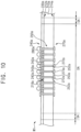
- FIG. 9 is an enlarged plan view illustrating portion 'B' in FIG. 6 .
- a first wafer W1 including a plurality of first semiconductor chips formed therein may be prepared.
- the first wafer W1 may include a first substrate 210a, a first front insulation layer 230a having first bonding pads 240a provided in an outer surface thereof, and/or a first backside insulation layer 260a. Additionally, the first wafer W1 may include first through electrodes 250a that are provided in the first substrate 210a and electrically connect the first and second bonding pads 240a and 270a to each other.
- the first substrate 210a may have a first surface 212a and a second surface 214a opposite to each other.
- the first substrate 210a may include a die region DA where circuit patterns and cells are formed and a scribe lane region SA surrounding the die region DA.
- the first substrate 210a may be sawed along the scribe lane region SA dividing the die regions DA of the first wafer W1 by a following singulation process to form an individual semiconductor chip.
- the first substrate 210a may include silicon, germanium, silicon-germanium, and/or III-V compounds, e.g., GaP, GaAs, GaSb, etc.
- the first substrate 210a may be a silicon-on-insulator (SOI) substrate, or a germanium-on-insulator (GOI) substrate.
- SOI silicon-on-insulator
- GOI germanium-on-insulator
- the circuit patterns may include a transistor, a capacitor, a diode, etc.
- the circuit patterns may constitute circuit elements.
- the first semiconductor chip may be a semiconductor device including a plurality of the circuit elements formed therein.
- the circuit patterns may be formed by performing a front end of line (FEOL) process for manufacturing a semiconductor device on the first surface 212a of the first substrate 210a.
- the surface of the first substrate on which the FEOL process is performed may be referred to as a front surface of the first substrate, and a surface opposite to the front surface may be referred to as a backside surface.
- the first front insulation layer 230a may be formed as an insulation interlayer on the first surface 212a, e.g., the front surface of the first substrate 210a.
- the first front insulation layer 230a may include a plurality of insulation layers and wirings in the insulation layers.
- the first bonding pads 240a may be provided in the outermost insulation layer of the first front insulation layer 230a.
- the first front insulation layer 230a may include a first insulation interlayer 220a and/or a second insulation interlayer 222a.
- the first insulation interlayer 220a may be provided on the first surface 212a of the first substrate 210a and may cover the circuit patterns 216a on the first surface 212a of the first substrate 210a.
- the first insulation interlayer 220a may include, for example, silicon oxide and/or a low dielectric material.
- the first insulation interlayer 220a may include lower wirings 217a in the first insulation interlayer 220a.
- the second insulation interlayer 222a may include buffer layers and insulation layers stacked alternately on one another.
- the buffer layer may include silicon nitride, silicon carbon nitride (SiCN), and/or silicon carbon oxynitride (SiCON), etc.
- the insulation layer may include silicon oxide, carbon doped silicon oxide, and/or silicon carbon nitride (SiCN), etc.
- the second insulation interlayer 222a may include a plurality of metal wirings 226a therein.
- the metal wiring 226a of the second insulation interlayer 222a may include metal lines and/or contacts electrically connected to each other.
- the first bonding pads 240a may be provided in the outermost insulation layer of the second front insulation layer 230a. The first bonding pads 240a may be exposed through an outer surface of the second front insulation layer 230a.
- the circuit pattern 216a may be electrically connected to the first bonding pad 240a by the lower wirings and the wirings.
- the first through electrode 250a may penetrate through the first insulation interlayer 220a and extend from the first surface 212a to the second surface 214a of the first substrate 210a.
- the first through electrode 250a may be electrically connected to the first bonding pad 240a by the wirings 226a.
- a liner layer 251a may be provided on an outer surface of the first through electrode 250a.
- the liner layer may include silicon oxide and/or carbon doped silicon oxide.
- the liner layer 251a may insulate electrically the first substrate 210a and/or the first front insulation layer 230a from the first through electrode 250a.
- the first backside insulation layer 260a may be formed on the second surface 214a, e.g., the backside surface of the first substrate 210a.
- the second bonding pads 270a may be provided in the first backside insulation layer 260a.
- the second bonding pads 270a may be arranged on an exposed surface of the first through electrode 250a.
- the first backside insulation layer 260a may include silicon oxide, carbon doped silicon oxide, and/or silicon carbon nitride (SiCN), etc. Accordingly, the first and second bonding pads 240a and 270a may be electrically connected to each other by the first through electrode 250a.
- the first through electrode 250a may be formed to penetrate through the first insulation interlayer 240a and extend to a predetermined (or alternately given) depth from the first surface 212a of the first substrate 210a (via middle process), the backside surface of the first substrate 210a, e.g., the second surface 214a may be grinded until end portions of the first through electrodes 250a are exposed, and then, the second backside insulation layer 260a having the second bonding pads 270a electrically connected to the exposed end portions of the first through electrodes 250a respectively may be formed on the second surface 214a of the first substrate 210a.
- the first and second bonding pads 240a and 270a may be arranged in respective pad arrays on the upper surface and the lower surface of the first semiconductor chip, and the first through electrodes 250a may be arranged in first regions R1 of the first substrate 210a in an array.
- the via array of the first through electrodes 250a may be designed to correspond to the pad arrays of the first and second bonding pads 240a and 270a.
- the first through electrodes 250a may include a first group of through electrodes 252a and/or a second group of through electrodes 253a alternately arranged in a first direction D1.
- the first group of through electrodes 252a may be arranged to be spaced apart from each other in the first direction D1.
- the second group of through electrodes 253a may be arranged to be spaced apart from each other in the first direction D2.
- Each, or one or more, of the second group of through electrodes 253a may be arranged between the first group of through electrodes 252a adjacent to each other.
- the first through electrodes may include first and/or second groups of through electrodes alternately arranged in a second direction D2 perpendicular to the first direction D1.
- a distance 2L between the adjacent first through electrodes 252a of the first group may be equal to a distance 2L between the adjacent through electrodes 253a of the second group.
- a distance L between the through electrode 252a of the first group and the through electrode 253a of the second group adjacent to each other may be half of the distance 2L between the adjacent through electrodes 252a of the first group.
- the first bonding pads 240a may include a first group of bonding pads 242a electrically connected to the first group of through electrodes 252a respectively and/or a second group of bonding pads 243a electrically connected to the second group of through electrodes 253a respectively.
- the first group of bonding pads 242a and the second group of bonding pads 243a may be alternately arranged in the first direction D1.
- the second bonding pads 270a may include a first group of bonding pads 272a electrically connected to the first group of through electrodes 252a respectively and/or a second group of bonding pads 273a electrically connected to the second group of through electrodes 253a respectively.
- the first group of bonding pads 272a and the second group of bonding pads 273a may be alternately arranged in the first direction D1.
- the circuit pattern 216a may include an input/output (I/O) circuitry 218a for transmitting data signals and an electrostatic discharge circuitry 219a associated with the I/O circuitry 218a.
- I/O input/output
- Each, or one or more, of the first group of through electrodes 252a and/or the second group of through electrodes 253a may be used as a portion of an input/output (I/O) path through which the data signals are transmitted.
- the first and second bonding pads 240a and 270a electrically connected to each other by the first group of through electrodes 252a and the second group of through electrodes 253a, respectively, may be used as input/output (I/O) pads.
- the first semiconductor chip may further include control signal through electrodes for transmitting control signals such as address and command, and control signal pads electrically connected to the control signal through electrodes.
- the first group of through electrodes 252a and/or the first group of bonding pads 242a and/or 272a may be selectively connected to the I/O circuitry 218a.
- the second group of through electrodes 253a and/or the second group of bonding pads 243a and/or 273a may not be connected to the I/O circuitry.
- the circuit pattern 216a may further include a fuse portion 215a capable of electrically decoupling the I/O circuitry 218a from the first group of through electrodes 252a and the first group of bonding pads 242a and 272a.
- the fuse portion may include a programmable fuse or an anti-fuse. Accordingly, the I/O circuitry 218a may be selectively connected to or disconnected from the first group of through electrodes 252a and the first group of connection pads 242a and 272a by the fuse portion.
- a second region R2 in which the I/O circuitry 218a and/or the electrostatic discharge circuitry 219a are formed may be provided around the first region R1 in which the first group of through electrodes 252a are formed.
- the first region R1 may be a TSV region
- the second region R2 may be an I/O circuit region. Since the second group of through electrodes 253a is not connected to the I/O circuitry, an additional I/O circuit region may not be provided around the region in which the second group of through electrodes 253a is formed.
- the second group of through electrodes 253a may be arranged between the first group of through electrodes 252a while maintaining the array of the first group of through electrodes 252a as it is.
- TSV I/O input/output
- first conductive connection members 280a may be formed on the first bonding pads 240a on the first surface 212a of the first substrate 210a.
- a seed layer may be formed on the first bonding pads 240a on the first surface 212a of the first substrate 210a, a photoresist pattern having openings that expose portions of the seed layer may be formed, a conductive material may be formed to fill the openings of the photoresist pattern, the photoresist pattern may be removed, and then, a reflow process may be performed to form bumps as the first conductive connection members 280a.
- the conductive material may be formed on the seed layer by an electroplating process.
- the bump may be formed by a screen printing process, and/or a deposition process, etc.
- the first conductive connection member may include a solder bump.
- the first wafer W1 may be cut along the scribe lane region SA to form an individual first semiconductor chip 200a.
- the first semiconductor chip 200a may be stacked on a base substrate 100 using a substrate support system WSS. After attaching the base substrate 100 to a carrier substrate using an adhesive film, the first semiconductor chip 200a may be stacked on the base substrate 100.
- the base substrate 100 may include a semiconductor die region in which an integrated circuit is integrated.
- the base substrate 100 may include a buffer die serving as a processor for controlling a memory device.
- the base substrate 100 may include an interposer having wires for electrical connection with a processor chip.
- the base substrate 100 may have an upper surface 102 and a lower surface 104 opposite to each other.
- Substrate pads 110 for electrical connection with the first semiconductor chip 200a may be provided on the upper surface 102 of the base substrate 100.
- Outer connection pads for electrical connection with an external device may be provided on the lower surface 104 of the base substrate 100.
- the first semiconductor chip 200a may be stacked on the base substrate 100 through the first conductive connection members 280a.
- the first semiconductor chip 200a may be arranged on the base substrate 100 such that the first bonding pad 240a of the first semiconductor chip 200a faces the substrate pad 110 of the base substrate 100.
- the first conductive connection members 280a may be interposed between the base substrate 100 and the first semiconductor chip 200a.
- the first conductive connection member 280a may electrically connect the substrate pad 110 of the base substrate 100 and the first bonding pad 240a of the first semiconductor chip 200a.
- a second semiconductor chip 200b may be stacked on the first semiconductor chip 200a.
- processes the same as or similar to those described with reference to FIGS. 6 to 11 may be performed to form an individualized second semiconductor chip 200b, and the second semiconductor chip 200b may be stacked on the first semiconductor chip 200a.
- the second semiconductor chip 200b may be identical to the first semiconductor chip 200a in terms of structural form.
- an arrangement of through electrodes and/or an arrangement of bonding pads of the second semiconductor chip 200b may be the same as the arrangement of the through electrodes and/or the arrangement of the bonding pads of the first semiconductor chip 200a.
- the second semiconductor chip 200b may be somewhat different from the first semiconductor chip 200a in terms of functionality. Employing semiconductor chips having the same structure in the stack may provide advantages in terms of manufacturing cost.
- the second semiconductor chip 200b may include a second substrate 210b, a second front insulation layer 230b having third bonding pads 240b on an outer surface thereof, a second backside insulation layer 260b having fourth bonding pads 270b therein, and/or second through electrodes 250b provided in the second substrate 210b and electrically connecting the third and fourth bonding pads 240b and 270b to each other.
- the second through electrodes 250b may include a first group of through electrodes 252b and/or a second group of through electrodes 253b alternately arranged in the first direction D1.
- the first group of through electrodes 252b may be selectively connected to an I/O circuitry 218b.
- the second group of through electrodes 253b may not be connected to the I/O circuitry 218b.
- the third bonding pads 240b may include a first group of bonding pads 242b electrically connected to the first group of through electrodes 252b respectively and/or a second group of bonding pads 243b electrically connected to the second group of through electrodes 253b respectively.
- the first group of bonding pads 242b and the second group of bonding pads 243b of the third bonding pads 240b may be alternately arranged in the first direction D1.
- the fourth bonding pads 270b may include a first group of bonding pads 272b electrically connected to the first group of through electrodes 252b respectively and/or a second group of bonding pads 273b electrically connected to the second group of through electrodes 253b respectively.
- the first group of bonding pads 272b and the second group of bonding pads 273b of the fourth bonding pads 270b may be alternately arranged in the first direction D1.
- the second semiconductor chip 200b may be stacked on the first semiconductor chip 200a through second conductive connection members 280b.
- the second semiconductor chip 200b may be arranged on the first semiconductor chip 200a such that the third bonding pad 240b of the second semiconductor chip 200b faces the second bonding pad 270a of the first semiconductor chip 200a.
- the second conductive connection members 280b may be interposed between the first semiconductor chip 200a and the second semiconductor chip 200b.
- the second conductive connection member 280b may electrically connect the second bonding pad 270a of the first semiconductor chip 200b and the third bonding pad 240b of the second semiconductor chip 200b.
- the second semiconductor chip 200b may be offset from the first semiconductor chip 200a by a preset (or alternately given) interval (-P) in the first direction such that the first group of through electrodes 252b of the second semiconductor chip 200b are electrically connected to the second group of through electrodes 253a of the first semiconductor chip 200a, respectively, and/or the second group of through electrodes 253b of the second semiconductor chip 200b are electrically connected to the first group of through electrodes 252a of the first semiconductor chip 200a, respectively.
- the preset (or alternately given) interval may be a distance between adjacent through electrodes, for example, a pitch.
- the first group of bonding pads 242b of the third bonding pads 240b of the second semiconductor chip 200b may be electrically connected to the second group of bonding pads 273a of the second bonding pads 270a of the first semiconductor chip 200a, respectively, and the second group of bonding pads 243b of the third bonding pads 240b of the second semiconductor chip 200b may be electrically connected to the first group of bonding pads 272a of the second bonding pads 270a of the first semiconductor chip 200a, respectively.
- a third semiconductor chip 200c may be stacked on the second semiconductor chip 200b.
- processes the same as or similar to those described with reference to FIGS. 6 to 11 may be performed to form an individualized third semiconductor chip 200c, and the third semiconductor chip 200c may be stacked on the second semiconductor chip 200b.
- the third semiconductor chip 200c may be identical to the first and/or second semiconductor chips 200a and 200b in terms of structural form.
- an arrangement of through electrodes and/or an arrangement of bonding pads of the third semiconductor chip 200c may be the same as the arrangement of the through electrodes and the arrangement of the bonding pads of the first and second semiconductor chips 200a and 200b.
- the third semiconductor chip 200c may be somewhat different from the first and/or second semiconductor chips 200a and 200b in terms of functionality. Employing semiconductor chips having the same structure in the stack may provide advantages in terms of manufacturing cost.
- the third semiconductor chip 200c may include a third substrate 210c, a third front insulation layer 230c having fifth bonding pads 240c on an outer surface thereof, a third backside insulation layer having sixth bonding pads 270c therein, and/or third through electrodes 250c provided in the third substrate 210c and electrically connecting the fifth and sixth bonding pads 240c and 270c to each other.
- the third through electrodes 250c may include a first group of through electrodes 252c and/or a second group of through electrodes 253c alternately arranged in the first direction.
- the first group of through electrodes 252c may be selectively connected to an I/O circuitry 218b.
- the second group of through electrodes 253c may not be connected to the I/O circuitry 218b.
- the fifth bonding pads 240c may include a first group of bonding pads 242c electrically connected to the first group of through electrodes 252c respectively and/or a second group of bonding pads 243c electrically connected to the second group of through electrodes 253c respectively.
- the first group of bonding pads 242c and the second group of bonding pads 243c of the fifth bonding pads 240c may be alternately arranged in the first direction D1.
- the sixth bonding pads 270c may include a first group of bonding pads 272c electrically connected to the first group of through electrodes 252c respectively and/or a second group of bonding pads 273c electrically connected to the second group of through electrodes 253c respectively.
- the first group of bonding pads 272c and the second group of bonding pads 273c of the sixth bonding pads 270c may be alternately arranged in the first direction D1.
- the third semiconductor chip 200c may be stacked on the second semiconductor chip 200b through third conductive connection members 280c.
- the third semiconductor chip 200c may be arranged on the second semiconductor chip 200b such that the fifth bonding pad 240c of the third semiconductor chip 200c faces the fourth bonding pad 270b of the second semiconductor chip 200b.
- the third conductive connection members 280c may be interposed between the second semiconductor chip 200b and the third semiconductor chip 200c.
- the third conductive connection member 280c may electrically connect the fourth bonding pad 270b of the second semiconductor chip 200b and the fifth bonding pad 240c of the third semiconductor chip 200c.
- the third semiconductor chip 200c may be offset from the second semiconductor chip 200b by a preset (or alternately given) interval (+P) in a reverse direction of the first direction such that the first group of through electrodes 252c of the third semiconductor chip 200c are electrically connected to the second group of through electrodes 253b of the second semiconductor chip 200b, respectively, and/or the second group of through electrodes 253c of the third semiconductor chip 200c are electrically connected to the first group of through electrodes 252b of the second semiconductor chip 200b, respectively.
- the preset (or alternately given) interval may be a distance between adjacent through electrodes, for example, a pitch.
- the first group of bonding pads 242c of the fifth bonding pads 240c of the third semiconductor chip 200c may be electrically connected to the second group of bonding pads 273b of the fourth bonding pads 270b of the second semiconductor chip 200b, respectively, and/or the second group of bonding pads 243c of the fifth bonding pads 240c of the third semiconductor chip 200c may be electrically connected to the first group of bonding pads 272b of the second bonding pads 270b of the second semiconductor chip 200b, respectively.
- a fourth semiconductor chip 200d may be stacked on the third semiconductor chip 200c.
- processes the same as or similar to those described with reference to FIGS. 6 to 11 may be performed to form an individualized fourth semiconductor chip 200d, and the fourth semiconductor chip 200d may be stacked on the third semiconductor chip 200c.
- the fourth semiconductor chip 200c may be identical to the first, second and/or third semiconductor chips 200a, 200b and 200c in terms of structural form.
- an arrangement of through electrodes and/or an arrangement of bonding pads of the fourth semiconductor chip 200d may be the same as the arrangement of the through electrodes and/or the arrangement of the bonding pads of the first, second and/or third semiconductor chips 200a, 200b and 200c.
- the fourth semiconductor chip 200d may include a fourth substrate 210d and/or a fourth front insulation layer 230d having seventh bonding pads 240d on an outer surface thereof.
- the seventh bonding pads 240d may include a first group of bonding pads 242d and/or a second group of bonding pads 243d alternately arranged in the first direction.
- the first group of bonding pads 242d may be selectively connected to an I/O circuitry 218b.
- the second group of bonding pads 243d may not be connected to the I/O circuitry 218b.
- the fourth semiconductor chip 200d may be stacked on the third semiconductor chip 200c through fourth conductive connection members 280d.
- the fourth semiconductor chip 200d may be arranged on the third semiconductor chip 200c such that the seventh bonding pad 240d of the fourth semiconductor chip 200d faces the sixth bonding pad 270c of the third semiconductor chip 200c.
- the fourth conductive connection members 280d may be interposed between the third semiconductor chip 200c and the fourth semiconductor chip 200d.
- the fourth conductive connection member 280d may electrically connect the sixth bonding pad 270c of the third semiconductor chip 200c and the seventh bonding pad 240d of the fourth semiconductor chip 200d.
- the fourth semiconductor chip 200d may be offset from the third semiconductor chip 200c by a preset (or alternately given) interval (-P) in the first direction such that the first group of bonding pads 242d of the seventh bonding pads 240d of the fourth semiconductor chip 200d are electrically connected to the second group of bonding pads 273c of the sixth bonding pads 270c of the third semiconductor chip 200c, respectively, and/or the second group of bonding pads 243d of the seventh bonding pads 240d of the fourth semiconductor chip 200d are electrically connected to the first group of bonding pads 272c of the sixth bonding pads 270c of the third semiconductor chip 200c, respectively.
- the preset (or alternately given) interval may be a distance between adjacent through electrodes, for example, a pitch.
- a molding member 300 may be formed on the base substrate 100 to cover the first to fourth semiconductor chips 200a, 200b, 200c and/or 200d.
- the molding member 300 may be formed to fill gaps between the base substrate 100 and the first to fourth semiconductor chips 200a, 200b, 200c and/or 200d.
- the molding member 300 may be formed using a polymer material such as epoxy molding compound (EMC).
- gaps between the base substrate 100 and the first to fourth semiconductor chips 200a, 200b, 200c and/or 200d may be filled by underfill members and/or adhesive films.
- the base substrate 100 and the molding member 300 may be cut along a cutting region to complete the semiconductor package 10 in FIG. 1 .
- FIG. 18 is a cross-sectional view illustrating a semiconductor package in accordance with some example embodiments.
- the semiconductor package may be substantially the same as or similar to the semiconductor package described with reference to FIGS. 1 to 3 except for arrangements of pads and through electrodes of first to fourth semiconductor chips.
- same reference numerals will be used to refer to the same or like elements and any further repetitive explanation concerning the above elements will be omitted.
- a semiconductor package 11 may include first to fourth semiconductor chips 200a, 200b, 200c and/or 200d sequentially stacked on one another.
- the second and/or fourth semiconductor chips 200b and 200d may be identical to the first and/or third semiconductor chips 200a and 200c in terms of structural form except for arrangements of through electrodes and bonding pads.
- First and/or second groups of through electrodes 252a and 253a of the first semiconductor chip 200a and/or first and/or second groups of through electrodes 252b and 253b of the second semiconductor chip 200b may be arranged to change their positions.
- the second group of through electrodes 253b of the second semiconductor chip 200b may be at the same position as the first position from the center of the second semiconductor chip 200b.
- the first group of through electrodes 252b of the second semiconductor chip 200b may be at the same position as the second position from the center of the second semiconductor chip 200b.
- first through electrodes 250a of the first semiconductor chip 200a and/or second through electrodes 250b of the second semiconductor chip 200b are disposed to overlap each other, the first group of through electrodes 252b of the second semiconductor chip 200b may be overlapped with the second group of through electrodes 253a of the first semiconductor chip 200a respectively and the second group of through electrodes 253b of the second semiconductor chip 200b may be overlapped with the first group of through electrodes 252a of the first semiconductor chip 200a respectively.
- a first group of through electrodes 252c of the third semiconductor chip 200c may be overlapped with the second group of through electrodes 253b of the second semiconductor chip 200b respectively and a second group of through electrodes 253c of the third semiconductor chip 200c may be overlapped with the first group of through electrodes 252b of the second semiconductor chip 200b respectively.
- a first group of through electrodes 252d of the fourth semiconductor chip 200d may be overlapped with the second group of through electrodes 253c of the third semiconductor chip 200c respectively and a second group of through electrodes 253d of the fourth semiconductor chip 200d may be overlapped with the first group of through electrodes 252c of the third semiconductor chip 200c respectively.
- the second semiconductor chip 200b may be stacked to completely (or substantially) overlap with the first semiconductor chip 200a without being offset from the first semiconductor chip 200a
- the third semiconductor chip 200c may be stacked to completely (or substantially) overlap with the second semiconductor chip 200b without being offset from the second semiconductor chip 200b
- the fourth semiconductor chip 200d may be stacked to completely (or substantially) overlap with the third semiconductor chip 200c without being offset from the third semiconductor chip 200c.
- the first group of bonding pads 242b of the third bonding pads 240b of the second semiconductor chip 200b may be electrically connected to the second group of bonding pads 273a of the second bonding pads 270a of the first semiconductor chip 200a respectively, and the second group of bonding pads 243b of the third bonding pads 240b of the second semiconductor chip 200b may be electrically connected to the first group of bonding pads 272a of the second bonding pads 270a of the first semiconductor chip 200a respectively.
- the first group of bonding pads 242c of the fifth bonding pads 240c of the third semiconductor chip 200c may be electrically connected to the second group of bonding pads 273b of the fourth second bonding pads 270b of the second semiconductor chip 200b respectively, and the second group of bonding pads 243c of the fifth bonding pads 240c of the third semiconductor chip 200c may be electrically connected to the first group of bonding pads 272b of the fourth bonding pads 270b of the second semiconductor chip 200b respectively.
- the first group of bonding pads 242d of the seventh bonding pads 240d of the fourth semiconductor chip 200d may be electrically connected to the second group of bonding pads 273c of the sixth bonding pads 270c of the third semiconductor chip 200c respectively, and the second group of bonding pads 243d of the seventh bonding pads 240d of the fourth semiconductor chip 200d may be electrically connected to the first group of bonding pads 272c of the sixth bonding pads 270c of the third semiconductor chip 200c respectively.
- FIG. 19 is a cross-sectional view illustrating transmission paths of data input/output (I/O) signals in the semiconductor package of FIG. 18 .
- a signal from an I/O circuitry 218d of the fourth semiconductor chip 200d may be transmitted to a base chip 100 through the second group of through electrodes 253c of the third semiconductor chip 200c, the first group of through electrodes 252b of the second semiconductor chip 200b and the second group of through electrodes 253a of the first semiconductor chip 200a.
- the second group of through electrodes 253c of the third semiconductor chip 200c, the first group of through electrodes 252b of the second semiconductor chip 200b and/or the second group of through electrodes 253a of the first semiconductor chip 200a may serve as an I/O signal path P1 which connects between the I/O circuitry 218d of the fourth semiconductor chip 200d and the base chip 100.
- a signal from an I/O circuitry 218c of the third semiconductor chip 200c may be transmitted to the base chip 100 through the second group of through electrodes 253b of the second semiconductor chip 200b and the first group of through electrodes 252a of the first semiconductor chip 200a.
- the second group of through electrodes 253b of the second semiconductor chip 200b and/or the first group of through electrodes 252a of the first semiconductor chip 200a may serve as an I/O signal path P2 which connects between the I/O circuitry 218c of the third semiconductor chip 200c and the base chip 100.
- a signal from an I/O circuitry 218b of the second semiconductor chip 200b may be transmitted to the base chip 100 through the second group of through electrodes 253a of the first semiconductor chip 200a.
- the second group of through electrodes 253a of the first semiconductor chip 200a may serve as an I/O signal path P3 which connects between the I/O circuitry 218b of the second semiconductor chip 200b and the base chip 100.
- Only one of every four bonding pads consecutively arranged in a given row may be operably connected to the I/O circuitry, defining a staggered I/O circuit pattern. This may allow for point-to-point connections between the base chip 100 and the first to fourth semiconductor chips 200a, 200b, 200c and/or 200d.
- FIGS. 20 to 25 are views illustrating a method of manufacturing a semiconductor package in accordance with some example embodiments.
- a first semiconductor chip 200a with first conductive connection members 280a attached thereto may be prepared.
- Processes the same as or similar to those described with reference to FIGS. 6 to 11 may be performed to form the first conductive connection members 280a on first bonding pads 240a of the first semiconductor chip 200a.
- the first semiconductor chip 200a may have a first surface and a second surface opposite to each other, and may include a plurality of first bonding pads 240a provided on the first surface, a plurality of second bonding pads 270a provided on the second surface, and/or a plurality of first through electrodes 250a electrically connecting the first and second bonding pads 240a and 270a.
- the first through electrodes 250a may include a first group of through electrodes 252a and/or a second group of through electrodes 253a alternately arranged in a first direction.
- the first group of through electrodes 252a may be arranged to be spaced apart from each other in the first direction.
- the second group of through electrodes 253a may be arranged to be spaced apart from each other in the first direction.
- Each, or one or more, of the second group of through electrodes 253a may be arranged between the first group of through electrodes 252a adjacent to each other.
- the first bonding pads 240a may include a first group of bonding pads 242a electrically connected to the first group of through electrodes 252a respectively and/or a second group of bonding pads 243a electrically connected to the second group of through electrodes 253a respectively.
- the first group of bonding pads 242a and the second group of bonding pads 243a may be alternately arranged in the first direction.
- the second bonding pads 270a may include a first group of bonding pads 272a electrically connected to the first group of through electrodes 252a respectively and/or a second group of bonding pads 273a electrically connected to the second group of through electrodes 253a respectively.
- the first group of bonding pads 272a and the second group of bonding pads 273a may be alternately arranged in the first direction.
- a second semiconductor chip 200b with second conductive connection members 280b attached thereto may be prepared.
- Processes the same as or similar to those described with reference to FIGS. 6 to 11 may be performed to form the second conductive connection members 280b on third bonding pads 240b of the second semiconductor chip 200b.
- the second semiconductor chip 200b may be identical to the first semiconductor chip 200a in terms of structural form except for arrangements of through electrodes and bonding pads.
- a first group of through electrodes 252b of the second semiconductor chip 200b may be overlapped with the second group of through electrodes 253a of the first semiconductor chip 200a respectively and/or a second group of through electrodes 253b of the second semiconductor chip 200b may be overlapped with the first group of through electrodes 252a of the first semiconductor chip 200a respectively.
- first and second bonding pads 240a and 270a of the first semiconductor chip 200a and third and fourth bonding pads 240b and 270b of the second semiconductor chip 200b are disposed to overlap each other, a first group of bonding pads 242b and 272b of the second semiconductor chip 200b may be overlapped with the second group of bonding pads 243a and 273a of the first semiconductor chip 200a respectively and/or a second group of bonding pads 243b and 273b of the second semiconductor chip 200b may be overlapped with the first group of bonding pads 242a and 272a of the first semiconductor chip 200a respectively.
- the first semiconductor chip 200a and the second semiconductor chip 200b may be sequentially stacked on a base substrate 100.
- the first semiconductor chip 200a may be stacked on the base substrate 100 using a substrate support system WSS. After attaching the base substrate 100 to a carrier substrate using an adhesive film, the first semiconductor chip 200a may be stacked on the base substrate 100.
- the first semiconductor chip 200a may be stacked on the base substrate 100 through the first conductive connection members 280a.
- the first semiconductor chip 200a may be arranged on the base substrate 100 such that the first bonding pad 240a of the first semiconductor chip 200a faces a substrate pad 110 of the base substrate 100.
- the second semiconductor chip 200b may be stacked on the first semiconductor chip 200a through the second conductive connection members 280b.
- the second semiconductor chip 200b may be arranged on the first semiconductor chip 200a such that the third bonding pad 240b of the second semiconductor chip 200b faces the second bonding pad 270a of the first semiconductor chip 200a.
- the first group of through electrodes 252b of the second semiconductor chip 200b may be electrically connected to the second group of through electrodes 253a of the first semiconductor chip 200a respectively and the second group of through electrodes 253b of the second semiconductor chip 200b may be electrically connected to the first group of through electrodes 252a of the first semiconductor chip 200a respectively.
- the second semiconductor chip 200b may be stacked to completely (or substantially) overlap with the first semiconductor chip 200a without being offset from the first semiconductor chip 200a.
- the first group of bonding pads 242b of the third bonding pads 240b of the second semiconductor chip 200b may be electrically connected to the second group of bonding pads 273a of the second bonding pads 270a of the first semiconductor chip 200a respectively, and the second group of bonding pads 243b of the third bonding pads 240b of the second semiconductor chip 200b may be electrically connected to the first group of bonding pads 272a of the second bonding pads 270a of the first semiconductor chip 200a respectively.
- a third semiconductor chip 200c may be stacked on the second semiconductor chip 200b.
- Processes the same as or similar to those described with reference to FIG. 20 may be performed to form third conductive connection members 280c on fifth bonding pads 240c of the third semiconductor chip 200c.
- the third semiconductor chip 200c may be identical to the first semiconductor chip 200a in terms of structural form.
- an arrangement of through electrodes and an arrangement of bonding pads of the third semiconductor chip 200c may be the same as the arrangement of the through electrodes and the arrangement of the bonding pads of the first semiconductor chip 200a.
- the third semiconductor chip 200c may be stacked on the second semiconductor chip 200b through the third conductive connection members 280c.
- the third semiconductor chip 200c may be arranged on the second semiconductor chip 200b such that fifth bonding pad 240c of the third semiconductor chip 200c faces the fourth bonding pad 270b of the second semiconductor chip 200b.
- a first group of through electrodes 252c of the third semiconductor chip 200c may be electrically connected to the second group of through electrodes 253b of the second semiconductor chip 200b respectively and a second group of through electrodes 253c of the third semiconductor chip 200c may be electrically connected to the first group of through electrodes 252b of the second semiconductor chip 200b respectively.
- the third semiconductor chip 200c may be stacked to completely (or substantially) overlap with the second semiconductor chip 200b without being offset from the second semiconductor chip 200b.
- a first group of bonding pads 242c of the fifth bonding pads 240c of the third semiconductor chip 200c may be electrically connected to the second group of bonding pads 273b of the fourth second bonding pads 270b of the second semiconductor chip 200b respectively, and/or a second group of bonding pads 243c of the fifth bonding pads 240c of the third semiconductor chip 200c may be electrically connected to the first group of bonding pads 272b of the fourth bonding pads 270b of the second semiconductor chip 200b respectively.
- a fourth semiconductor chip 200d may be stacked on the third semiconductor chip 200c.
- Processes the same as or similar to those described with reference to FIG. 20 may be performed to form fourth conductive connection members 280d on seventh bonding pads 240d of the fourth semiconductor chip 200d.
- the fourth semiconductor chip 200d may be identical to the second semiconductor chip 200b in terms of structural form.
- an arrangement of through electrodes and an arrangement of bonding pads of the fourth semiconductor chip 200d may be the same as the arrangement of the through electrodes and the arrangement of the bonding pads of the second semiconductor chip 200b.
- a first group of through electrodes 252d of the fourth semiconductor chip 200d may be electrically connected to the second group of through electrodes 253c of the third semiconductor chip 200c respectively and/or a second group of through electrodes 253d of the fourth semiconductor chip 200d may be electrically connected to the first group of through electrodes 252c of the third semiconductor chip 200c respectively.
- the fourth semiconductor chip 200d may be stacked to completely (or substantially) overlap with the third semiconductor chip 200c without being offset from the third semiconductor chip 200c.
- a first group of bonding pads 242d of the seventh bonding pads 240d of the fourth semiconductor chip 200d may be electrically connected to the second group of bonding pads 273c of the sixth second bonding pads 270c of the third semiconductor chip 200c respectively, and/or a second group of bonding pads 243d of the seventh bonding pads 240d of the fourth semiconductor chip 200d may be electrically connected to the first group of bonding pads 272c of the sixth bonding pads 270c of the third semiconductor chip 200c respectively.
- a molding member 300 may be formed on the base substrate 100 to cover the first to fourth semiconductor chips 200a, 200b, 200c and/or 200d.
- the molding member 400 may be formed to fill gaps between the base substrate 100 and the first to fourth semiconductor chips 200a, 200b, 200c and/or 200d.
- the molding member 400 may be formed using a polymer material such as epoxy molding compound (EMC).
- gaps between the base substrate 100 and the first to fourth semiconductor chips 200a, 200b, 200c and/or 200d may be filled by underfill members and/or adhesive films.
- the base substrate 100 and the molding member 300 may be cut along a cutting region to complete the semiconductor package 11 in FIG. 18 .
- the semiconductor package may include semiconductor devices such as logic devices or memory devices.
- the semiconductor package may include logic devices such as central processing units (CPUs), main processing units (MPUs), or application processors (APs), or the like, and volatile memory devices such as DRAM devices, HBM devices, or non-volatile memory devices such as flash memory devices, PRAM devices, MRAM devices, ReRAM devices, or the like.
- logic devices such as central processing units (CPUs), main processing units (MPUs), or application processors (APs), or the like
- volatile memory devices such as DRAM devices, HBM devices, or non-volatile memory devices such as flash memory devices, PRAM devices, MRAM devices, ReRAM devices, or the like.
Landscapes
- Engineering & Computer Science (AREA)
- Microelectronics & Electronic Packaging (AREA)
- Semiconductor Integrated Circuits (AREA)
Applications Claiming Priority (1)
| Application Number | Priority Date | Filing Date | Title |
|---|---|---|---|
| KR1020210106801A KR102938111B1 (ko) | 2021-08-12 | 2021-08-12 | 반도체 패키지 및 반도체 패키지의 제조 방법 |
Publications (2)
| Publication Number | Publication Date |
|---|---|
| EP4135030A2 true EP4135030A2 (de) | 2023-02-15 |
| EP4135030A3 EP4135030A3 (de) | 2023-02-22 |
Family
ID=81327391
Family Applications (1)
| Application Number | Title | Priority Date | Filing Date |
|---|---|---|---|
| EP22166449.3A Pending EP4135030A3 (de) | 2021-08-12 | 2022-04-04 | Halbleiterpaket und verfahren zum herstellen des halbleiterpakets |
Country Status (4)
| Country | Link |
|---|---|
| US (1) | US12588551B2 (de) |
| EP (1) | EP4135030A3 (de) |
| KR (1) | KR102938111B1 (de) |
| CN (1) | CN115706096A (de) |
Cited By (1)
| Publication number | Priority date | Publication date | Assignee | Title |
|---|---|---|---|---|
| US12532729B2 (en) * | 2022-07-19 | 2026-01-20 | Samsung Electronics Co., Ltd. | Semiconductor package |
Families Citing this family (1)
| Publication number | Priority date | Publication date | Assignee | Title |
|---|---|---|---|---|
| CN119050051A (zh) * | 2024-10-28 | 2024-11-29 | 湖北星辰技术有限公司 | 半导体封装结构的形成方法 |
Citations (1)
| Publication number | Priority date | Publication date | Assignee | Title |
|---|---|---|---|---|
| KR20210106801A (ko) | 2020-02-21 | 2021-08-31 | 삼성전자주식회사 | 조성물, 이로부터 형성된 필름, 표시 장치, 물품 및 물품 제조방법 |
Family Cites Families (14)
| Publication number | Priority date | Publication date | Assignee | Title |
|---|---|---|---|---|
| WO2004038798A2 (en) | 2002-10-22 | 2004-05-06 | Unitive International Limited | Stacked electronic structures including offset substrates |
| US7494846B2 (en) * | 2007-03-09 | 2009-02-24 | Taiwan Semiconductor Manufacturing Company, Ltd. | Design techniques for stacking identical memory dies |
| WO2010138480A2 (en) | 2009-05-26 | 2010-12-02 | Rambus Inc. | Stacked semiconductor device assembly |
| KR20100135091A (ko) | 2009-06-16 | 2010-12-24 | 삼성전자주식회사 | 적층형 반도체 장치 및 이를 포함하는 반도체 시스템 |
| US9142262B2 (en) | 2009-10-23 | 2015-09-22 | Rambus Inc. | Stacked semiconductor device |
| US9123552B2 (en) * | 2010-03-30 | 2015-09-01 | Micron Technology, Inc. | Apparatuses enabling concurrent communication between an interface die and a plurality of dice stacks, interleaved conductive paths in stacked devices, and methods for forming and operating the same |
| US9449913B2 (en) | 2011-10-28 | 2016-09-20 | Intel Corporation | 3D interconnect structure comprising fine pitch single damascene backside metal redistribution lines combined with through-silicon vias |
| US8817547B2 (en) * | 2012-12-10 | 2014-08-26 | Micron Technology, Inc. | Apparatuses and methods for unit identification in a master/slave memory stack |
| KR102012505B1 (ko) * | 2012-12-20 | 2019-08-20 | 에스케이하이닉스 주식회사 | 토큰 링 루프를 갖는 스택 패키지 |
| KR20160000953A (ko) | 2014-06-25 | 2016-01-06 | 삼성전자주식회사 | 기판 및 반도체 패키지의 제조방법 |
| KR102264548B1 (ko) | 2014-11-21 | 2021-06-16 | 삼성전자주식회사 | 반도체 패키지 및 그 제조 방법 |
| JP6800788B2 (ja) * | 2017-03-15 | 2020-12-16 | キオクシア株式会社 | 半導体記憶装置 |
| KR102712310B1 (ko) | 2018-12-14 | 2024-10-04 | 삼성전자주식회사 | 반도체 패키지 및 반도체 패키지의 제조 방법 |
| KR20210031046A (ko) | 2019-09-11 | 2021-03-19 | 삼성전자주식회사 | 반도체 패키지 및 반도체 패키지의 제조 방법 |
-
2021
- 2021-08-12 KR KR1020210106801A patent/KR102938111B1/ko active Active
-
2022
- 2022-04-04 EP EP22166449.3A patent/EP4135030A3/de active Pending
- 2022-04-12 US US17/718,402 patent/US12588551B2/en active Active
- 2022-08-05 CN CN202210937420.7A patent/CN115706096A/zh active Pending
Patent Citations (1)
| Publication number | Priority date | Publication date | Assignee | Title |
|---|---|---|---|---|
| KR20210106801A (ko) | 2020-02-21 | 2021-08-31 | 삼성전자주식회사 | 조성물, 이로부터 형성된 필름, 표시 장치, 물품 및 물품 제조방법 |
Cited By (1)
| Publication number | Priority date | Publication date | Assignee | Title |
|---|---|---|---|---|
| US12532729B2 (en) * | 2022-07-19 | 2026-01-20 | Samsung Electronics Co., Ltd. | Semiconductor package |
Also Published As
| Publication number | Publication date |
|---|---|
| KR102938111B1 (ko) | 2026-03-13 |
| US20230049855A1 (en) | 2023-02-16 |
| KR20230024714A (ko) | 2023-02-21 |
| CN115706096A (zh) | 2023-02-17 |
| US12588551B2 (en) | 2026-03-24 |
| EP4135030A3 (de) | 2023-02-22 |
Similar Documents
| Publication | Publication Date | Title |
|---|---|---|
| EP3657538B1 (de) | Halbleitergehäuse | |
| CN110047810B (zh) | 半导体封装件以及包括其的半导体器件 | |
| CN103700633B (zh) | 半导体封装件 | |
| US11824045B2 (en) | Semiconductor package and method of manufacturing the semiconductor package | |
| US12237302B2 (en) | Semiconductor package | |
| EP4135030A2 (de) | Halbleiterpaket und verfahren zum herstellen des halbleiterpakets | |
| KR20160090706A (ko) | 협폭 인터포저를 갖는 반도체 패키지 | |
| US10403572B2 (en) | Semiconductor device and semiconductor package including the same | |
| US20240021575A1 (en) | Semiconductor package | |
| US9305902B1 (en) | Chip package and method for forming the same | |
| KR20110123504A (ko) | 크기 가변형 반도체 칩 및 이를 포함하는 웨이퍼 및 이를 이용한 반도체 패키지 | |
| JP2013085007A (ja) | ビアを介して電力供給及び接地されるパッケージ | |
| US12368136B2 (en) | Semiconductor package and a method of manufacturing the semiconductor package | |
| US20240413026A1 (en) | Semiconductor package and method of manufacturing the semiconductor package | |
| US20250105182A1 (en) | Semiconductor chip and semiconductor package including the same | |
| KR102882367B1 (ko) | 고성능 하이브리드 본딩을 위한 패드 패턴이 적용된 반도체 소자 | |
| US20260082986A1 (en) | Semiconductor package and manufacturing method of the same, and manufacturing method of semiconductor device for reconstitution process | |
| TWI917778B (zh) | 半導體封裝及其製造方法 | |
| JP7766043B2 (ja) | 半導体パッケージアセンブリ及び製造方法 | |
| KR102739100B1 (ko) | 반도체 패키지 구조 및 그 제조 방법 | |
| US20260040967A1 (en) | Package-package interconnection for solder joint fail redundancy and high bandwidth application | |
| US20240194643A1 (en) | Semiconductor package including a plurality of different stacked chips and method of manufacturing the semiconductor package | |
| US20230223350A1 (en) | Semiconductor package and method of fabricating the same | |
| KR20250159817A (ko) | 반도체 패키지 | |
| KR20250122817A (ko) | 반도체 패키지 및 이의 제조 방법 |
Legal Events
| Date | Code | Title | Description |
|---|---|---|---|
| PUAI | Public reference made under article 153(3) epc to a published international application that has entered the european phase |
Free format text: ORIGINAL CODE: 0009012 |
|
| STAA | Information on the status of an ep patent application or granted ep patent |
Free format text: STATUS: REQUEST FOR EXAMINATION WAS MADE |
|
| PUAL | Search report despatched |
Free format text: ORIGINAL CODE: 0009013 |
|
| 17P | Request for examination filed |
Effective date: 20220404 |
|
| AK | Designated contracting states |
Kind code of ref document: A2 Designated state(s): AL AT BE BG CH CY CZ DE DK EE ES FI FR GB GR HR HU IE IS IT LI LT LU LV MC MK MT NL NO PL PT RO RS SE SI SK SM TR |
|
| AK | Designated contracting states |
Kind code of ref document: A3 Designated state(s): AL AT BE BG CH CY CZ DE DK EE ES FI FR GB GR HR HU IE IS IT LI LT LU LV MC MK MT NL NO PL PT RO RS SE SI SK SM TR |
|
| RIC1 | Information provided on ipc code assigned before grant |
Ipc: G11C 5/06 20060101ALI20230117BHEP Ipc: G11C 5/04 20060101ALI20230117BHEP Ipc: G11C 5/02 20060101ALI20230117BHEP Ipc: H01L 25/065 20060101AFI20230117BHEP |
|
| P01 | Opt-out of the competence of the unified patent court (upc) registered |
Effective date: 20230519 |
|
| RBV | Designated contracting states (corrected) |
Designated state(s): AL AT BE BG CH CY CZ DE DK EE ES FI FR GB GR HR HU IE IS IT LI LT LU LV MC MK MT NL NO PL PT RO RS SE SI SK SM TR |