EP4132232A1 - Fpcb and manufacturing method therefor - Google Patents
Fpcb and manufacturing method therefor Download PDFInfo
- Publication number
- EP4132232A1 EP4132232A1 EP21849866.5A EP21849866A EP4132232A1 EP 4132232 A1 EP4132232 A1 EP 4132232A1 EP 21849866 A EP21849866 A EP 21849866A EP 4132232 A1 EP4132232 A1 EP 4132232A1
- Authority
- EP
- European Patent Office
- Prior art keywords
- conductive wire
- fpcb
- top surface
- circuit layer
- lower conductive
- Prior art date
- Legal status (The legal status is an assumption and is not a legal conclusion. Google has not performed a legal analysis and makes no representation as to the accuracy of the status listed.)
- Granted
Links
Images









Classifications
-
- H—ELECTRICITY
- H05—ELECTRIC TECHNIQUES NOT OTHERWISE PROVIDED FOR
- H05K—PRINTED CIRCUITS; CASINGS OR CONSTRUCTIONAL DETAILS OF ELECTRIC APPARATUS; MANUFACTURE OF ASSEMBLAGES OF ELECTRICAL COMPONENTS
- H05K1/00—Printed circuits
- H05K1/02—Details
- H05K1/0286—Programmable, customizable or modifiable circuits
- H05K1/0293—Individual printed conductors which are adapted for modification, e.g. fusable or breakable conductors, printed switches
-
- H—ELECTRICITY
- H01—ELECTRIC ELEMENTS
- H01H—ELECTRIC SWITCHES; RELAYS; SELECTORS; EMERGENCY PROTECTIVE DEVICES
- H01H85/00—Protective devices in which the current flows through a part of fusible material and this current is interrupted by displacement of the fusible material when this current becomes excessive
- H01H85/02—Details
- H01H85/04—Fuses, i.e. expendable parts of the protective device, e.g. cartridges
- H01H85/05—Component parts thereof
- H01H85/055—Fusible members
- H01H85/08—Fusible members characterised by the shape or form of the fusible member
-
- H—ELECTRICITY
- H05—ELECTRIC TECHNIQUES NOT OTHERWISE PROVIDED FOR
- H05K—PRINTED CIRCUITS; CASINGS OR CONSTRUCTIONAL DETAILS OF ELECTRIC APPARATUS; MANUFACTURE OF ASSEMBLAGES OF ELECTRICAL COMPONENTS
- H05K1/00—Printed circuits
- H05K1/16—Printed circuits incorporating printed electric components, e.g. printed resistors, capacitors or inductors
-
- H—ELECTRICITY
- H01—ELECTRIC ELEMENTS
- H01H—ELECTRIC SWITCHES; RELAYS; SELECTORS; EMERGENCY PROTECTIVE DEVICES
- H01H69/00—Apparatus or processes for the manufacture of emergency protective devices
- H01H69/02—Manufacture of fuses
- H01H69/022—Manufacture of fuses of printed circuit fuses
-
- H—ELECTRICITY
- H01—ELECTRIC ELEMENTS
- H01H—ELECTRIC SWITCHES; RELAYS; SELECTORS; EMERGENCY PROTECTIVE DEVICES
- H01H85/00—Protective devices in which the current flows through a part of fusible material and this current is interrupted by displacement of the fusible material when this current becomes excessive
- H01H85/02—Details
- H01H85/04—Fuses, i.e. expendable parts of the protective device, e.g. cartridges
- H01H85/041—Fuses, i.e. expendable parts of the protective device, e.g. cartridges characterised by the type
- H01H85/046—Fuses formed as printed circuits
-
- H—ELECTRICITY
- H05—ELECTRIC TECHNIQUES NOT OTHERWISE PROVIDED FOR
- H05K—PRINTED CIRCUITS; CASINGS OR CONSTRUCTIONAL DETAILS OF ELECTRIC APPARATUS; MANUFACTURE OF ASSEMBLAGES OF ELECTRICAL COMPONENTS
- H05K1/00—Printed circuits
- H05K1/02—Details
- H05K1/09—Use of materials for the conductive, e.g. metallic pattern
-
- H—ELECTRICITY
- H05—ELECTRIC TECHNIQUES NOT OTHERWISE PROVIDED FOR
- H05K—PRINTED CIRCUITS; CASINGS OR CONSTRUCTIONAL DETAILS OF ELECTRIC APPARATUS; MANUFACTURE OF ASSEMBLAGES OF ELECTRICAL COMPONENTS
- H05K1/00—Printed circuits
- H05K1/02—Details
- H05K1/11—Printed elements for providing electric connections to or between printed circuits
- H05K1/115—Via connections; Lands around holes or via connections
-
- H—ELECTRICITY
- H05—ELECTRIC TECHNIQUES NOT OTHERWISE PROVIDED FOR
- H05K—PRINTED CIRCUITS; CASINGS OR CONSTRUCTIONAL DETAILS OF ELECTRIC APPARATUS; MANUFACTURE OF ASSEMBLAGES OF ELECTRICAL COMPONENTS
- H05K3/00—Apparatus or processes for manufacturing printed circuits
- H05K3/22—Secondary treatment of printed circuits
- H05K3/28—Applying non-metallic protective coatings
- H05K3/281—Applying non-metallic protective coatings by means of a preformed insulating foil
-
- H—ELECTRICITY
- H05—ELECTRIC TECHNIQUES NOT OTHERWISE PROVIDED FOR
- H05K—PRINTED CIRCUITS; CASINGS OR CONSTRUCTIONAL DETAILS OF ELECTRIC APPARATUS; MANUFACTURE OF ASSEMBLAGES OF ELECTRICAL COMPONENTS
- H05K3/00—Apparatus or processes for manufacturing printed circuits
- H05K3/40—Forming printed elements for providing electric connections to or between printed circuits
- H05K3/4038—Through-connections; Vertical interconnect access [VIA] connections
-
- H—ELECTRICITY
- H01—ELECTRIC ELEMENTS
- H01H—ELECTRIC SWITCHES; RELAYS; SELECTORS; EMERGENCY PROTECTIVE DEVICES
- H01H85/00—Protective devices in which the current flows through a part of fusible material and this current is interrupted by displacement of the fusible material when this current becomes excessive
- H01H85/02—Details
- H01H85/04—Fuses, i.e. expendable parts of the protective device, e.g. cartridges
- H01H85/05—Component parts thereof
- H01H85/055—Fusible members
- H01H85/06—Fusible members characterised by the fusible material
-
- H—ELECTRICITY
- H01—ELECTRIC ELEMENTS
- H01H—ELECTRIC SWITCHES; RELAYS; SELECTORS; EMERGENCY PROTECTIVE DEVICES
- H01H85/00—Protective devices in which the current flows through a part of fusible material and this current is interrupted by displacement of the fusible material when this current becomes excessive
- H01H85/02—Details
- H01H85/04—Fuses, i.e. expendable parts of the protective device, e.g. cartridges
- H01H85/05—Component parts thereof
- H01H85/143—Electrical contacts; Fastening fusible members to such contacts
-
- H—ELECTRICITY
- H05—ELECTRIC TECHNIQUES NOT OTHERWISE PROVIDED FOR
- H05K—PRINTED CIRCUITS; CASINGS OR CONSTRUCTIONAL DETAILS OF ELECTRIC APPARATUS; MANUFACTURE OF ASSEMBLAGES OF ELECTRICAL COMPONENTS
- H05K1/00—Printed circuits
- H05K1/02—Details
- H05K1/03—Use of materials for the substrate
- H05K1/0393—Flexible materials
-
- H—ELECTRICITY
- H05—ELECTRIC TECHNIQUES NOT OTHERWISE PROVIDED FOR
- H05K—PRINTED CIRCUITS; CASINGS OR CONSTRUCTIONAL DETAILS OF ELECTRIC APPARATUS; MANUFACTURE OF ASSEMBLAGES OF ELECTRICAL COMPONENTS
- H05K2201/00—Indexing scheme relating to printed circuits covered by H05K1/00
- H05K2201/10—Details of components or other objects attached to or integrated in a printed circuit board
- H05K2201/10007—Types of components
- H05K2201/10181—Fuse
-
- H—ELECTRICITY
- H05—ELECTRIC TECHNIQUES NOT OTHERWISE PROVIDED FOR
- H05K—PRINTED CIRCUITS; CASINGS OR CONSTRUCTIONAL DETAILS OF ELECTRIC APPARATUS; MANUFACTURE OF ASSEMBLAGES OF ELECTRICAL COMPONENTS
- H05K2203/00—Indexing scheme relating to apparatus or processes for manufacturing printed circuits covered by H05K3/00
- H05K2203/07—Treatments involving liquids, e.g. plating, rinsing
- H05K2203/0703—Plating
- H05K2203/072—Electroless plating, e.g. finish plating or initial plating
-
- H—ELECTRICITY
- H05—ELECTRIC TECHNIQUES NOT OTHERWISE PROVIDED FOR
- H05K—PRINTED CIRCUITS; CASINGS OR CONSTRUCTIONAL DETAILS OF ELECTRIC APPARATUS; MANUFACTURE OF ASSEMBLAGES OF ELECTRICAL COMPONENTS
- H05K2203/00—Indexing scheme relating to apparatus or processes for manufacturing printed circuits covered by H05K3/00
- H05K2203/07—Treatments involving liquids, e.g. plating, rinsing
- H05K2203/0703—Plating
- H05K2203/0733—Method for plating stud vias, i.e. massive vias formed by plating the bottom of a hole without plating on the walls
Definitions
- the present invention relates to an FPCB and a method for manufacturing the same, and more specifically, to an FPCP which does not require a fuse to be mounted thereon, thereby reducing the total volume and saving costs, and a method for manufacturing the same.
- PCB printed circuit board
- FPCB flexible printed circuit board
- an FPCB is manufactured by laminating a copper foil on a polyimide film to form a copper clad laminate, laminating a dry film thereon to form a conductor pattern though exposure, development, and etching processes, and then attach a cover lay on the outermost copper foil.
- the FPCB is installed in a bent state inside a complex product case by utilizing the flexibility of raw materials or is used at a repeatedly moving portion, and due to the properties thereof, is used in various manners in miniaturization (digital cameras, camcorders, etc.), flexibility (printer heads, hard disks, etc.), high-density wires (precision instruments such as medical devices), and rationalization of assembly (measuring instruments, vehicle electronics, battery modules, etc.).
- the FPCB is formed by etching and the like, and thus, does not occupy a large volume, and does not frequently cause problems such as disconnection due to an external impact.
- elements such as a fuse are mounted on the FPCB separately through a mounting process after the FPCB is completely manufactured. Therefore, there have been problems in that the total volume of the FPCB increases, and costs also increase.
- Patent Document 1 Korean Patent Publication No. 1845714
- An object of the present invention for solving the above problems is to provide an FPCB which does not require a fuse to be mounted thereon, thereby reducing the total volume and saving costs, and a method for manufacturing the same.
- the pattern circuit layer has a pattern fuse embedded therein, and the pattern fuse includes: a first conductive wire made of a metal and having a spiral structure; and a second conductive wire made of a metal and having a spiral structure, wherein the first conductive wire and the second conductive wire have a double helix structure.
- the first conductive wire may include: a first lower conductive wire formed on a bottom surface of the pattern circuit layer; a first upper conductive wire formed on an top surface of the pattern circuit layer; and a first via conductive wire configured to connect the first lower conductive wire and the first upper conductive wire to each other
- the second conductive wire may include: a second lower conductive wire formed on the bottom surface of the pattern circuit layer; a second upper conductive wire formed on the top surface of the pattern circuit layer; and a second via conductive wire configured to connect the second lower conductive wire and the second upper conductive wire to each other.
- first conductive wire and the second conductive wire may have a quadrangular shape and a double helix structure.
- each of the first lower conductive wire, the second lower conductive wire, the first upper conductive wire, and the second upper conductive wire may be formed to have a linear shape.
- each of the first via conductive wire and the second via conductive wire may be formed to have a linear shape in a thickness direction on the pattern circuit layer.
- each of the first conductive wire and the second conductive wire may have a start terminal and an end terminal, which are exposed on only one of the top surface or the bottom surface of the pattern circuit layer.
- start terminal of the first conductive wire and the start terminal of the second conductive wire may be separately formed, and the end terminal of the first conductive wire and the end terminal of the second conductive wire may also be separately formed.
- start terminal of the first conductive wire and the start terminal of the second conductive wire may be formed connected to each other, and the end terminal of the first conductive wire and the end terminal of the second conductive wire may be formed connected to each other.
- each of the first conductive wire and the second conductive wire may have the start terminal connected to a power bus bar and the end terminal connected to a sensing bus bar.
- the end terminal of the first conductive wire may be connected to a first sensing bus bar, and the end terminal of the second conductive wire may be connected to a second bus bar.
- the metal may include at least one of silver, copper, gold, or aluminum.
- a cover lay may be further laminated on the top surface of the pattern circuit layer.
- a method for manufacturing an FPCB according to an embodiment of the present invention for achieving the above objects includes: forming a first lower conductive wire and a second lower conductive wire on an top surface of a base film; exposing both ends of the first lower conductive wire and the second lower conductive wire, and laminating a micro-pillar on the top surface of the base film; forming a first via conductive wire and a second via conductive wire on both the ends of the first lower conductive wire and the second lower conductive wire, respectively; injecting a filler into an empty space in which the micro-pillar is not filled on the top surface of the base film; and forming a first upper conductive wire connecting the first via conductive wires to each other and a second upper conductive wire connecting the second via conductive wires to each other on an top surface of the micro-pillar.
- the first lower conductive wire and the second lower conductive wire may be formed parallel to a first direction.
- the first upper conductive wire and the second upper conductive wire may be formed parallel to a second direction.
- first direction and the second direction may be directions different from each other.
- the first lower conductive wire and the second lower conductive wire may be formed on the top surface of the base film by at least one of an etching or printing method.
- the first upper conductive wire and the second upper conductive wire may be formed on the top surface of the micro-pillar by at least one of an etching or printing method.
- a first conductive wire including the first lower conductive wire, the first via conductive wire, and the first upper conductive wire, and a second conductive wire including the second lower conductor, the second via conductor, and the second upper conductor may each have a start terminal formed at a start portion, and an end terminal formed at an end portion.
- first conductive wire and the second conductive wire may have the start terminal and the end terminal, which are exposed only on one of an top surface or a bottom surface of a pattern circuit layer.
- the pattern fuse having the double helix structure is formed on the FPCB using the through polymer via (TPV) method rather than the mounting method and the like, it is possible to reduce the total volume of the FPCB and save the costs.
- TPV through polymer via
- inventive concept may, however, be embodied in different forms and should not be construed as limited to the embodiments set forth herein. Rather, these embodiments are provided so that this disclosure will be thorough and complete, and will fully convey the scope of the inventive concept to those skilled in the art to which the inventive concept pertains. The inventive concept will only be defined by the appended claims.
- the same reference numerals refer to like elements throughout the specification.
- FIG. 1 is a perspective view of a FPCB 1 which has a pattern fuse 100 embedded therein according to an embodiment of the present invention.
- the pattern fuse 100 having a double helix structure is formed on the FPCB 1 using a through polymer via (TPV) method rather than a mounting method and the like, it is possible to reduce the total volume of the FPCB 1 and save costs.
- TPV through polymer via
- the pattern circuit layer 10 has the pattern fuse 100 embedded therein, and the pattern fuse 100 includes a first conductive wire 101 made of a metal and spirally formed, and a second conductive wire 102 made of a metal and spirally formed.
- the first conductive wire 101 and the second conductive wire 102 have a double helix structure.
- the pattern fuse 100 includes the first conductive wire 101 and the second conductive wire 102.
- the first conductive wire 101 is made of a metal, and is embedded in the pattern circuit layer 10 of the FPCB 1.
- the second conductive wire 102 is also made of a metal, and is embedded in the pattern circuit layer 10 of the FPCB 1. Both the first conductive wire 101 and the second conductive wire 102 have spiral structures, and particularly, a double helix structure.
- the first conductive wire 101 includes a first lower conductive wire 1011, a first upper conductive wire 1013, and a first via conductive wire 1012.
- the first lower conductive wire 1011 is formed to have a linear shape on a bottom surface of the pattern circuit layer 10
- the first upper conductive wire 1013 is formed to have a linear shape on a top surface of the pattern circuit layer 10.
- the first via conductive wire 1012 connects the first lower conductive wire 1011 and the first upper conductive wire 1013 to each other, and is formed to have a linear shape in a thickness direction on the pattern circuit layer 10.
- the first conductive wire 101 may have a quadrangular shape.
- the first conductive wire 101 may have the spiral structure.
- the second conductive wire 102 includes a second lower conductive wire 1021, a second upper conductive wire 1023, and a second via conductive wire 1022.
- the second lower conductive wire 1021 is formed to have a linear shape on the bottom surface of the pattern circuit layer 10
- the second upper conductive wire 1023 is formed to have a linear shape on the top surface of the pattern circuit layer 10.
- the second via conductive wire 1022 connects the second lower conductive wire 1021 and the second upper conductive wire 1023 to each other, and is formed to have a linear shape in the thickness direction on the pattern circuit layer 10.
- the second conductive wire 102 may have a quadrangular shape.
- the second conductive wire 102 may have the spiral structure.
- the first conductive wire 101 and the second conductive wire 102 are not separately formed, but rather spirally formed in the state of overlapping each other, that is, have the double helix structure.
- the metal for forming the first conductive wire 101 and the second conductive wire 102 may include at least one of silver, copper, gold, or aluminum which has high electrical conductivity, and particularly, may preferably include copper, which is easy to be molded, has a low price, and is economical.
- FIG. 2 is a flowchart illustrating a method for manufacturing the FPCB 1 which has the pattern fuse 100 embedded therein according to an embodiment of the present invention.
- a method for manufacturing the FPCB 1 includes a process of forming a first lower conductive wire 1011 and a second lower conductive wire 1021 on a top surface of a base film 11; a process of exposing both ends of the first lower conductive wire 1011 and the second lower conductive wire 1021, and laminating a micro-pillar 103 on the top surface of the base film 11; a process of forming the first via conductive wire 1012 and the second via conductive wire 1022 on both the ends of the first lower conductive wire 1011 and the second lower conductive wire 1021, respectively; a process of injecting a filler 104 into an empty space in which the micro-pillar 103 is not filled on the top surface of the base film 11, and a process of forming the first upper conductive wire 1013 connecting the first via conductive wires 1012 to each other and the second upper conductive wire 1023 connecting the second via conductive wires 1022 to each to other on a top surface of the micro-pillar 103.
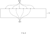
- FIG. 3 is a schematic side view illustrating a state in which a first lower conductive wire 1011 and a second lower conductive wire 1021 are formed on a base film 11 according to an embodiment of the present invention
- FIG. 4 is a schematic top view illustrating the state in which the first lower conductive wire 1011 and the second lower conductive wire 1021 are formed on the base film 11 according to an embodiment of the present invention.
- the base film 11 is prepared, and as illustrated in FIG. 3 , the first lower conductive wire 1011 and the second lower conductive wire 1021 are formed on an top surface of the base film 11 (S201).
- the base film 11 may be a film containing silicon.
- the first lower conductive wire 1011 and the second lower conductive wire 1021 may be formed on the top surface of the base film 11 by at least one of an etching or printing method.
- the first lower conductive wire 1011 and the second lower conductive wire 1021 are each provided in plurality, and may be formed parallel to a first direction.
- the first direction may have, for example, as illustrated in FIG. 4 , a predetermined inclination with respect to the base film 11.
- the first lower conductive wire 1011 and the second lower conductive wire 1021 may be alternately formed with each other. Therefore, later, the first conductive wire 101 and the second conductive wire 102 may have the double helix structure.
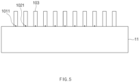
- FIG. 5 is a schematic side view illustrating a state in which a micro-pillar 103 is formed on the base film 11 according to an embodiment of the present invention
- FIG. 6 is a schematic top view illustrating the state in which the micro-pillar 103 is formed on the base film 11 according to an embodiment of the present invention.
- both the ends of the first lower conductive wire 1011 and the second lower conductive wire 1021 are exposed as illustrated in FIG. 5 , and the micro-pillar 103 is laminated on the top surface of the base film 11 (S202).
- the micro-pillar 103 are provided in plurality, and as illustrated in FIG. 6 , and may be formed parallel to a second direction which is different from the first direction.
- the first upper conductive wire 1013 and the second upper conductive wire 1023 are formed along the micro-pillar 103. Therefore, ends of different first lower conductive wires 1011 may be disposed on both the ends of one micro-pillar 103, respectively, or ends of different second lower conductive wires 1021 may be disposed on both the ends of one micro-pillar 103, respectively.
- a thick photoresist may be first laminated and then patterned.
- the micro-pillar 103 may be an epoxy-based SU-8 negative photoresist which is crosslinked by ultraviolet rays and of which remaining portions are washed to facilitate the patterning.
- a separate seed layer may be formed to activate the micro-pillar 103.
- a physical vapor deposition (PVD) method may be used, or an atomic layer deposition (ALD) method may be used.
- the seed layer may include nitride titanium (TiN) having electrical conductivity, good adhesion to a metal, and a low processing temperature.
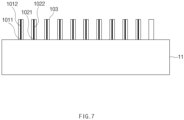
- FIG. 7 is a schematic side view illustrating a state in which a first via conductive wire 1012 and a second via conductive wire 1022 are formed on the base film 11 according to an embodiment of the present invention.
- the first via conductive wire 1012 and the second via conductive wire 1022 may be respectively formed at both the ends of the first lower conductive wire 1011 and the second lower conductive wire 1021 S203.
- ends of different first lower conductive wires 1011 may be disposed on both the ends of the micro-pillar 103, respectively, or ends of different second lower conductive wire 1021 may be disposed on both the ends of the micro-pillar 103, respectively. Therefore, when the first via conductive wire 1012 and the second via conductive wire 1022 are formed, as illustrated in FIG. 7 , the first via conductive wire 1012 and the second via conductive wire 1022 may be formed along sidewalls of both the ends of the micro-pillar 103.
- the micro-pillar 103 may be subjected to electroless plating with a metal such as copper.
- electrolytic plating may be additionally performed with a metal having low ionization tendency.
- Each of the first via conductive wire 1012 and the second via conductive wire 1022 is also made of a metal, and when the first conductive wire 1013 and the second conductive wire 1023 are formed later, the first via conductive wire 1012 and the second via conductive wire 1022 respectively connect the lower conductive wires 1011 and 1021 and the upper conductive wires 1021 and 1022, and thus, serve as a through electrode configured to electrically connect the bottom surface and the top surface of the pattern circuit layer 10 to each other.
- FIG. 8 is a schematic side view illustrating a state in which a filler 104 is injected into the base film 11 according to an embodiment of the present invention
- FIG. 9 is a schematic top view illustrating the state in which the filler 104 is injected into the base film 11 according to an embodiment of the present invention.
- the filler 104 is injected into an empty space in which the micro-pillar 103 is not filled (S204).
- the filler 104 may be an epoxy molding composition (EMC) having electrical insulation.
- EMC epoxy molding composition
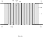
- FIG. 10 is a schematic top view illustrating a state in which a first upper conductive wire 1013 and a second upper conductive wire 1023 are formed according to an embodiment of the present invention.
- the first upper conductive wire 1013 connecting the first via conductive wires 1012 to each other and the second upper conductive wire 1023 connecting the second via conductive wires 1022 to each other are formed S205.
- the first upper conductive wire 1021 and the second upper conductive wire 1023 may be formed on the top surface of the base film 103 by at least one of an etching or printing method.
- the first upper conductive wire 1013 and the second upper conductive wire 1023 are all formed along the micro-pillar 103. That is, the first upper conductive wire 1013 may be formed on the top surface of the micro-pillar 103 on which the first via conductive wire 1012 is formed, while connecting the first via conductive wires 1012 to each other, the second upper conductive wire 1023 may be formed on the top surface of the micro-pillar 103 on which the second via conductive wire 1022 is formed, while connecting the first via conductive wires 1012 to each other.
- the first upper conductive wire 1013 and the second upper conductive wire1023 may be formed to be wider than the first via conductive wire 1012 and the second via conductive wire 1022 to be connected to the first via conductive wire 1012 and the second via conductive wire 1022, respectively.
- ends of different first lower wires 1011 may be disposed on both the ends of one micro-pillar 103, respectively, or ends of different second lower wires 1021 may be disposed on both the ends of one micro-pillar 103, respectively. Therefore, the first upper conductive wire 1013 is connected to each of the different first lower conductive wires 1011 through the first via conductive wire 1012, and the second upper conductive wire 1023 is connected to each of the different second lower conductive wires 1021 through the second via conductive wire 1012, so that the first conductive wire 101 and the second conductive wire 102 may be spirally formed.
- the first upper conductive wire 1013 and the second upper conductive wire 1023 are each provided in plurality, and are all formed along the micro-pillar 103, and thus, may be formed parallel to the second direction. It is preferable that the second direction is a direction different from the first direction. For example, as illustrated in FIG. 10 , the second direction may have a predetermined inclination with respect to the first direction. In addition the first upper conductive wire 1013 and the second upper conductive wire 1023 may be alternately formed with each other. Therefore, in the pattern circuit layer 10 of the FPCB 1, the pattern fuse 100 including the first conductive wire 101 and the second lead 102 having a double helix structure may be formed embedded. Furthermore, after the pattern fuse 100 is formed, the base film 11 may be removed.
- a cover lay may be laminated on the top surface of the micro-pillar 103.
- the cover lay may be a film of a polyimide-based material.
- FIG. 11 is a perspective view illustrating a state in which start terminals 1014 and 1024 and end terminals 1015 and 1025 are formed on a first conductive wire 101 and a second conductive wire 102 according to an embodiment of the present invention.
- the start terminals 1014 and 1024 are formed at start portions of the first conductive wire 101 and the second conductive wire 102, and the end terminals 1015 and 1025 are formed at end portions thereof.
- the first conductive wire 101 and the second conductive wire 102 may have the start terminals 1014 and 1024 and the end terminals 1015 and 1025 all exposed only on one of the top surface or the bottom surface of the pattern circuit layer 10.
- the first conductive wire 101 and the second conductive wire 102 have the start terminals 1014 and 1024 and the end terminals 1015 and 1025 all separately formed. That is, as illustrated in FIG. 11 , at the start portion of the first conductive wire 101, a first start terminal 1014 is formed, and at the start portion of the second conductive wire 102, a second start terminal 1024 is separately formed. In addition, at the end portion of the first conductive wire 101, a first end terminal 1015 is formed, and at the end portion of the second conductive wire 102, a second end terminal 1025 is separately formed.
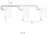
- FIG. 12 is a schematic view illustrating a state in which bus bars 21 and 22 are connected to the pattern fuse 100 according to an embodiment of the present invention.
- the upper and bottom surfaces of the FPCB 1 should be bent to be inverted from each other. Then, a process of bending the FPCB 1 should be further added, and there is also a problem in that the durability of a bent portion is degraded to cause lifespan to be shortened.
- the first start terminal 1014 of the first conductive wire 101 and the second start terminal 1024 of the second conductive wire 102 are, as illustrated in FIG. 12 , connected to one power bus bar 21.
- the first start terminal 1014 and the second start terminal 1024 are all exposed on the same surface of the pattern circuit layer 10, so that when connected to the power bus bar 21, the top surface and the bottom surface of the FPCB 1 are not required to be bent to be inverted from each other.
- first end terminal 1015 of the first conductive wire 101 and the second end terminal 1025 of the second conductive wire 102 are connected to different sensing bus bars 221 and 222, respectively.
- first end terminal 1015 and the second end terminal 1025 are all exposed on the same surface of the pattern circuit layer 10, so that when connected to the sensing bus bar 22, the top surface and the bottom surface of the FPCB 1 are not required to be bent to be inverted from each other.
- FIG. 13 is a perspective view illustrating the state in which a start terminal 105 and an end terminal 106 are formed on the first conductive wire 101 and the second conductive wire 102 according to another embodiment of the present invention.
- the first conductive wire 101 and the second conductive wire 102 have the start terminal 105 and the end terminal 106 formed respectively connected to each other. That is, as illustrated in FIG. 13 , a first start terminal formed in a start portion of the first conductive wire 101 and a second start terminal formed in a start portion of the second conductive wire 102 are formed connected to each other. In addition, a first end terminal formed in an end portion of the first conductive wire 101 and a second end terminal formed in an end portion of the second conductive wire 102 are formed connected to each other. Particularly, as illustrated in FIG.
- the first start terminal and the second start terminal may be integrally formed as one start terminal 105, and the first end terminal and the second end terminal may be integrally formed as one end terminal 106.
- the first start terminal and the second start terminal and the first end terminal and the second end terminal may be separately formed and then bonded to each other through a separate bonding part (not shown), or may be connected to each other through welding or an adhesive.
- the first conductive wire 101 and the second conductive wire 102 may have the start terminal 105 and the end terminal 106 all exposed only on one of the top surface or the bottom surface of the pattern circuit layer 10.
- FIG. 14 is a schematic view illustrating a state in which bus bars 21a and 22a are connected to a pattern fuse 100a according to another embodiment of the present invention.
- the start terminals 105 of the first conductive wire 101 and the second conductive wire 102 are formed connected to each other, and thus, are connected to one power bus bar 21a as illustrated in FIG. 14 .
- the first start terminal and the second start terminal are all exposed on the same surface of the pattern circuit layer 10 and then connected to each other, so that when connected to the power bus bar 21a, an top surface and a bottom surface of an FPCB 1a are not required to be bent to be inverted from each other.
- the end terminals 106 of the first conductive wire 101 and the second conductive wire 102 are also formed connected to each other, and thus, are connected to one sensing bus bar 22a.
- the first end terminal and the second end terminal are all exposed on the same surface of the pattern circuit layer 10, so that when connected to the sensing bus bar 22a, the top surface and the bottom surface of the FPCB 1a are not required to be bent to be inverted from each other.
Landscapes
- Engineering & Computer Science (AREA)
- Microelectronics & Electronic Packaging (AREA)
- Manufacturing & Machinery (AREA)
- Structure Of Printed Boards (AREA)
- Fuses (AREA)
- Printing Elements For Providing Electric Connections Between Printed Circuits (AREA)
- Parts Printed On Printed Circuit Boards (AREA)
Abstract
Description
- The present application claims the benefit of the priority of
Korean Patent Application No. 10-2020-0094041, filed on July 28, 2020 - The present invention relates to an FPCB and a method for manufacturing the same, and more specifically, to an FPCP which does not require a fuse to be mounted thereon, thereby reducing the total volume and saving costs, and a method for manufacturing the same.
- A printed circuit board (PCB) is widely used in various electronic products such as TVs, computers, mobile phones, displays, communication networks, and semiconductor modules. As a type of such PCB, a flexible printed circuit board (FPCB) with flexibility in particular has recently been widely used.
- In general, an FPCB is manufactured by laminating a copper foil on a polyimide film to form a copper clad laminate, laminating a dry film thereon to form a conductor pattern though exposure, development, and etching processes, and then attach a cover lay on the outermost copper foil. The FPCB is installed in a bent state inside a complex product case by utilizing the flexibility of raw materials or is used at a repeatedly moving portion, and due to the properties thereof, is used in various manners in miniaturization (digital cameras, camcorders, etc.), flexibility (printer heads, hard disks, etc.), high-density wires (precision instruments such as medical devices), and rationalization of assembly (measuring instruments, vehicle electronics, battery modules, etc.).
- The FPCB is formed by etching and the like, and thus, does not occupy a large volume, and does not frequently cause problems such as disconnection due to an external impact. However, elements such as a fuse are mounted on the FPCB separately through a mounting process after the FPCB is completely manufactured. Therefore, there have been problems in that the total volume of the FPCB increases, and costs also increase.
- (Patent Document 1)
Korean Patent Publication No. 1845714 - An object of the present invention for solving the above problems is to provide an FPCB which does not require a fuse to be mounted thereon, thereby reducing the total volume and saving costs, and a method for manufacturing the same.
- Problems to be solved by the present invention are not limited to the above-mentioned problem, and other problems that are not mentioned may be apparent to those skilled in the art from the following description.
- In an FPCB including a pattern circuit layer according to an embodiment of the present invention for achieving the above objects, the pattern circuit layer has a pattern fuse embedded therein, and the pattern fuse includes: a first conductive wire made of a metal and having a spiral structure; and a second conductive wire made of a metal and having a spiral structure, wherein the first conductive wire and the second conductive wire have a double helix structure.
- In addition, the first conductive wire may include: a first lower conductive wire formed on a bottom surface of the pattern circuit layer; a first upper conductive wire formed on an top surface of the pattern circuit layer; and a first via conductive wire configured to connect the first lower conductive wire and the first upper conductive wire to each other, and the second conductive wire may include: a second lower conductive wire formed on the bottom surface of the pattern circuit layer; a second upper conductive wire formed on the top surface of the pattern circuit layer; and a second via conductive wire configured to connect the second lower conductive wire and the second upper conductive wire to each other.
- In addition, the first conductive wire and the second conductive wire may have a quadrangular shape and a double helix structure.
- In addition, each of the first lower conductive wire, the second lower conductive wire, the first upper conductive wire, and the second upper conductive wire may be formed to have a linear shape.
- In addition, each of the first via conductive wire and the second via conductive wire may be formed to have a linear shape in a thickness direction on the pattern circuit layer.
- In addition, each of the first conductive wire and the second conductive wire may have a start terminal and an end terminal, which are exposed on only one of the top surface or the bottom surface of the pattern circuit layer.
- In addition, the start terminal of the first conductive wire and the start terminal of the second conductive wire may be separately formed, and the end terminal of the first conductive wire and the end terminal of the second conductive wire may also be separately formed.
- In addition, the start terminal of the first conductive wire and the start terminal of the second conductive wire may be formed connected to each other, and the end terminal of the first conductive wire and the end terminal of the second conductive wire may be formed connected to each other.
- In addition, each of the first conductive wire and the second conductive wire may have the start terminal connected to a power bus bar and the end terminal connected to a sensing bus bar.
- In addition, the end terminal of the first conductive wire may be connected to a first sensing bus bar, and the end terminal of the second conductive wire may be connected to a second bus bar.
- In addition, the metal may include at least one of silver, copper, gold, or aluminum.
- In addition, a cover lay may be further laminated on the top surface of the pattern circuit layer.
- A method for manufacturing an FPCB according to an embodiment of the present invention for achieving the above objects includes: forming a first lower conductive wire and a second lower conductive wire on an top surface of a base film; exposing both ends of the first lower conductive wire and the second lower conductive wire, and laminating a micro-pillar on the top surface of the base film; forming a first via conductive wire and a second via conductive wire on both the ends of the first lower conductive wire and the second lower conductive wire, respectively; injecting a filler into an empty space in which the micro-pillar is not filled on the top surface of the base film; and forming a first upper conductive wire connecting the first via conductive wires to each other and a second upper conductive wire connecting the second via conductive wires to each other on an top surface of the micro-pillar.
- In addition, in the forming of the first lower conductive wire and the second lower conductive wire, the first lower conductive wire and the second lower conductive wire may be formed parallel to a first direction.
- In addition, in the forming of the first upper conductive wire and the second upper conductive wire, the first upper conductive wire and the second upper conductive wire may be formed parallel to a second direction.
- In addition, the first direction and the second direction may be directions different from each other.
- In addition, in the forming of the first lower conductive wire and the second lower conductive wire, the first lower conductive wire and the second lower conductive wire may be formed on the top surface of the base film by at least one of an etching or printing method.
- In addition, in the forming of the first upper conductive wire and the second upper conductive wire, the first upper conductive wire and the second upper conductive wire may be formed on the top surface of the micro-pillar by at least one of an etching or printing method.
- In addition, after the forming of the first upper conductive wire and the second upper conductive wire, a first conductive wire including the first lower conductive wire, the first via conductive wire, and the first upper conductive wire, and a second conductive wire including the second lower conductor, the second via conductor, and the second upper conductor may each have a start terminal formed at a start portion, and an end terminal formed at an end portion.
- In addition, the first conductive wire and the second conductive wire may have the start terminal and the end terminal, which are exposed only on one of an top surface or a bottom surface of a pattern circuit layer.
- Other specific details of the present invention are included in the detailed description and drawings.
- According to the embodiments of the present invention, there are at least the following effects.
- Since the pattern fuse having the double helix structure is formed on the FPCB using the through polymer via (TPV) method rather than the mounting method and the like, it is possible to reduce the total volume of the FPCB and save the costs.
- Effects according to the present invention are not limited by the contents exemplified above, and more various effects are included herein.
-
-
FIG. 1 is a perspective view of a FPCB 1 which has apattern fuse 100 embedded therein according to an embodiment of the present invention. -
FIG. 2 is a flowchart illustrating a method for manufacturing the FPCB 1 which has thepattern fuse 100 embedded therein according to an embodiment of the present invention. -
FIG. 3 is a schematic side view illustrating a state in which a first lowerconductive wire 1011 and a second lowerconductive wire 1021 are formed on abase film 11 according to an embodiment of the present invention. -
FIG. 4 is a schematic top view illustrating the state in which the first lowerconductive wire 1011 and the second lowerconductive wire 1021 are formed on thebase film 11 according to an embodiment of the present invention. -
FIG. 5 is a schematic side view illustrating a state in which a micro-pillar 103 is formed on thebase film 11 according to an embodiment of the present invention. -
FIG. 6 is a schematic top view illustrating the state in which the micro-pillar 103 is formed on thebase film 11 according to an embodiment of the present invention. -
FIG. 7 is a schematic side view illustrating a state in which a first viaconductive wire 1012 and a second viaconductive wire 1022 are formed on thebase film 11 according to an embodiment of the present invention. -
FIG. 8 is a schematic side view illustrating a state in which afiller 104 is injected into thebase film 11 according to an embodiment of the present invention. -
FIG. 9 is a schematic top view illustrating the state in which thefiller 104 is injected into thebase film 11 according to an embodiment of the present invention. -
FIG. 10 is a schematic top view illustrating a state in which a first upperconductive wire 1013 and a second upperconductive wire 1023 are formed according to an embodiment of the present invention. -
FIG. 11 is a perspective view illustrating a state in which startterminals end terminals conductive wire 101 and a secondconductive wire 102 according to an embodiment of the present invention. -
FIG. 12 is a schematic view illustrating a state in whichbus bars pattern fuse 100 according to an embodiment of the present invention. -
FIG. 13 is a perspective view illustrating the state in which astart terminal 105 and anend terminal 106 are formed on the firstconductive wire 101 and the secondconductive wire 102 according to another embodiment of the present invention. -
FIG. 14 is a schematic view illustrating a state in whichbus bars pattern fuse 100a according to another embodiment of the present invention. - Advantages and features of the inventive concept and methods of accomplishing the same may be understood more readily by reference to the following detailed description of exemplary embodiments and the accompanying drawings. The inventive concept may, however, be embodied in different forms and should not be construed as limited to the embodiments set forth herein. Rather, these embodiments are provided so that this disclosure will be thorough and complete, and will fully convey the scope of the inventive concept to those skilled in the art to which the inventive concept pertains. The inventive concept will only be defined by the appended claims. The same reference numerals refer to like elements throughout the specification.
- Unless otherwise defined, all the terms used herein (including technical and scientific terms) will be used in a sense that can be commonly understood to those of ordinary skill in the art to which the inventive concept pertains. In addition, the terms that are defined in a commonly used dictionary are not interpreted ideally or excessively unless specifically defined.
- The terms used herein are for the purpose of describing embodiments and are not intended to be limiting of the present invention. In the present disclosure, singular forms include plural forms unless the context clearly indicates otherwise. As used herein, the terms "comprises" and/or "comprising" are intended to be inclusive of the stated elements, and do not exclude the possibility of the presence or the addition of one or more other elements.
- Hereinafter, preferred embodiments of the present invention will be described in detail with reference to the accompanying drawings.
-
FIG. 1 is a perspective view of aFPCB 1 which has apattern fuse 100 embedded therein according to an embodiment of the present invention. - According to an embodiment of the present invention, since the
pattern fuse 100 having a double helix structure is formed on theFPCB 1 using a through polymer via (TPV) method rather than a mounting method and the like, it is possible to reduce the total volume of theFPCB 1 and save costs. - To this end, in the
FPCB 1 including apattern circuit layer 10 according to an embodiment of the present invention, thepattern circuit layer 10 has thepattern fuse 100 embedded therein, and thepattern fuse 100 includes a firstconductive wire 101 made of a metal and spirally formed, and a secondconductive wire 102 made of a metal and spirally formed. The firstconductive wire 101 and the secondconductive wire 102 have a double helix structure. - As illustrated in
FIG. 1 , thepattern fuse 100 according to an embodiment of the present invention includes the firstconductive wire 101 and the secondconductive wire 102. The firstconductive wire 101 is made of a metal, and is embedded in thepattern circuit layer 10 of theFPCB 1. In addition, the secondconductive wire 102 is also made of a metal, and is embedded in thepattern circuit layer 10 of theFPCB 1. Both the firstconductive wire 101 and the secondconductive wire 102 have spiral structures, and particularly, a double helix structure. - Specifically, the first
conductive wire 101 includes a first lowerconductive wire 1011, a first upperconductive wire 1013, and a first viaconductive wire 1012. The first lowerconductive wire 1011 is formed to have a linear shape on a bottom surface of thepattern circuit layer 10, and the first upperconductive wire 1013 is formed to have a linear shape on a top surface of thepattern circuit layer 10. In addition, the first viaconductive wire 1012 connects the first lowerconductive wire 1011 and the first upperconductive wire 1013 to each other, and is formed to have a linear shape in a thickness direction on thepattern circuit layer 10. Since the first lowerconductive wire 1011, the first upperconductive wire 1013, and the first viaconductive wire 1012 each have the linear shape as described above, the firstconductive wire 101 may have a quadrangular shape. In addition, since the first lowerconductive wire 1011, the first viaconductive wire 1012, and the first upperconductive wire 1013 are sequentially connected and repeatedly formed, the firstconductive wire 101 may have the spiral structure. - In the same manner, the second
conductive wire 102 includes a second lowerconductive wire 1021, a second upperconductive wire 1023, and a second viaconductive wire 1022. The second lowerconductive wire 1021 is formed to have a linear shape on the bottom surface of thepattern circuit layer 10, and the second upperconductive wire 1023 is formed to have a linear shape on the top surface of thepattern circuit layer 10. In addition, the second viaconductive wire 1022 connects the second lowerconductive wire 1021 and the second upperconductive wire 1023 to each other, and is formed to have a linear shape in the thickness direction on thepattern circuit layer 10. Since the second lowerconductive wire 1021, the second upperconductive wire 1023, and the second viaconductive wire 1022 each have the linear shape as described above, the secondconductive wire 102 may have a quadrangular shape. In addition, since the second lowerconductive wire 1021, the second viaconductive wire 1022, and the second upperconductive wire 1023 are sequentially connected and repeatedly formed, the secondconductive wire 102 may have the spiral structure. - The first
conductive wire 101 and the secondconductive wire 102 are not separately formed, but rather spirally formed in the state of overlapping each other, that is, have the double helix structure. In addition, the metal for forming the firstconductive wire 101 and the secondconductive wire 102 may include at least one of silver, copper, gold, or aluminum which has high electrical conductivity, and particularly, may preferably include copper, which is easy to be molded, has a low price, and is economical. -
FIG. 2 is a flowchart illustrating a method for manufacturing theFPCB 1 which has thepattern fuse 100 embedded therein according to an embodiment of the present invention. - A method for manufacturing the
FPCB 1 according to an embodiment of the present invention includes a process of forming a first lowerconductive wire 1011 and a second lowerconductive wire 1021 on a top surface of abase film 11; a process of exposing both ends of the first lowerconductive wire 1011 and the second lowerconductive wire 1021, and laminating a micro-pillar 103 on the top surface of thebase film 11; a process of forming the first viaconductive wire 1012 and the second viaconductive wire 1022 on both the ends of the first lowerconductive wire 1011 and the second lowerconductive wire 1021, respectively; a process of injecting afiller 104 into an empty space in which the micro-pillar 103 is not filled on the top surface of thebase film 11, and a process of forming the first upperconductive wire 1013 connecting the first viaconductive wires 1012 to each other and the second upperconductive wire 1023 connecting the second viaconductive wires 1022 to each to other on a top surface of the micro-pillar 103. - Hereinafter, each step illustrated in the flow chart of
FIG. 2 will be described in detail with reference toFIG. 3 to FIG. 10 . -
FIG. 3 is a schematic side view illustrating a state in which a first lowerconductive wire 1011 and a second lowerconductive wire 1021 are formed on abase film 11 according to an embodiment of the present invention, andFIG. 4 is a schematic top view illustrating the state in which the first lowerconductive wire 1011 and the second lowerconductive wire 1021 are formed on thebase film 11 according to an embodiment of the present invention. - First, the
base film 11 is prepared, and as illustrated inFIG. 3 , the first lowerconductive wire 1011 and the second lowerconductive wire 1021 are formed on an top surface of the base film 11 (S201). Thebase film 11 may be a film containing silicon. In addition, the first lowerconductive wire 1011 and the second lowerconductive wire 1021 may be formed on the top surface of thebase film 11 by at least one of an etching or printing method. - The first lower
conductive wire 1011 and the second lowerconductive wire 1021 are each provided in plurality, and may be formed parallel to a first direction. In addition, the first direction may have, for example, as illustrated inFIG. 4 , a predetermined inclination with respect to thebase film 11. In addition, the first lowerconductive wire 1011 and the second lowerconductive wire 1021 may be alternately formed with each other. Therefore, later, the firstconductive wire 101 and the secondconductive wire 102 may have the double helix structure. -
FIG. 5 is a schematic side view illustrating a state in which a micro-pillar 103 is formed on thebase film 11 according to an embodiment of the present invention, andFIG. 6 is a schematic top view illustrating the state in which the micro-pillar 103 is formed on thebase film 11 according to an embodiment of the present invention. - When the first lower
conductive wire 1011 and the second lowerconductive wire 1021 are formed, both the ends of the first lowerconductive wire 1011 and the second lowerconductive wire 1021 are exposed as illustrated inFIG. 5 , and the micro-pillar 103 is laminated on the top surface of the base film 11 (S202). At this time, the micro-pillar 103 are provided in plurality, and as illustrated inFIG. 6 , and may be formed parallel to a second direction which is different from the first direction. In addition, later, the first upperconductive wire 1013 and the second upperconductive wire 1023 are formed along the micro-pillar 103. Therefore, ends of different first lowerconductive wires 1011 may be disposed on both the ends of onemicro-pillar 103, respectively, or ends of different second lowerconductive wires 1021 may be disposed on both the ends of onemicro-pillar 103, respectively. - In order to laminate the micro-pillar 103, a thick photoresist may be first laminated and then patterned. The micro-pillar 103 may be an epoxy-based SU-8 negative photoresist which is crosslinked by ultraviolet rays and of which remaining portions are washed to facilitate the patterning.
- Meanwhile, although not shown in the drawings, after the micro-pillar 103 is laminated, a separate seed layer may be formed to activate the micro-pillar 103. In order to form the seed layer, a physical vapor deposition (PVD) method may be used, or an atomic layer deposition (ALD) method may be used. In addition, the seed layer may include nitride titanium (TiN) having electrical conductivity, good adhesion to a metal, and a low processing temperature.
-
FIG. 7 is a schematic side view illustrating a state in which a first viaconductive wire 1012 and a second viaconductive wire 1022 are formed on thebase film 11 according to an embodiment of the present invention. - After the micro-pillar 103 is laminated, the first via
conductive wire 1012 and the second viaconductive wire 1022 may be respectively formed at both the ends of the first lowerconductive wire 1011 and the second lowerconductive wire 1021 S203. As described above, ends of different first lowerconductive wires 1011 may be disposed on both the ends of the micro-pillar 103, respectively, or ends of different second lowerconductive wire 1021 may be disposed on both the ends of the micro-pillar 103, respectively. Therefore, when the first viaconductive wire 1012 and the second viaconductive wire 1022 are formed, as illustrated inFIG. 7 , the first viaconductive wire 1012 and the second viaconductive wire 1022 may be formed along sidewalls of both the ends of the micro-pillar 103. - In order to form the first via
conductive wire 1012 and the second viaconductive wire 1022, the micro-pillar 103 may be subjected to electroless plating with a metal such as copper. In addition, in order to prevent corrosion of the metal, electrolytic plating may be additionally performed with a metal having low ionization tendency. - Each of the first via
conductive wire 1012 and the second viaconductive wire 1022 is also made of a metal, and when the firstconductive wire 1013 and the secondconductive wire 1023 are formed later, the first viaconductive wire 1012 and the second viaconductive wire 1022 respectively connect the lowerconductive wires conductive wires pattern circuit layer 10 to each other. -
FIG. 8 is a schematic side view illustrating a state in which afiller 104 is injected into thebase film 11 according to an embodiment of the present invention, andFIG. 9 is a schematic top view illustrating the state in which thefiller 104 is injected into thebase film 11 according to an embodiment of the present invention. - As illustrated in
FIGS. 8 and9 , on the top surface of thebase film 11, thefiller 104 is injected into an empty space in which the micro-pillar 103 is not filled (S204). Thefiller 104 may be an epoxy molding composition (EMC) having electrical insulation. Thereby, the micro-pillar 103 may be encapsulated inside the insulator. -
FIG. 10 is a schematic top view illustrating a state in which a first upperconductive wire 1013 and a second upperconductive wire 1023 are formed according to an embodiment of the present invention. - On the top surface of the micro-pillar 103, the first upper
conductive wire 1013 connecting the first viaconductive wires 1012 to each other and the second upperconductive wire 1023 connecting the second viaconductive wires 1022 to each other are formed S205. In addition, the first upperconductive wire 1021 and the second upperconductive wire 1023 may be formed on the top surface of thebase film 103 by at least one of an etching or printing method. - The first upper
conductive wire 1013 and the second upperconductive wire 1023 are all formed along the micro-pillar 103. That is, the first upperconductive wire 1013 may be formed on the top surface of the micro-pillar 103 on which the first viaconductive wire 1012 is formed, while connecting the first viaconductive wires 1012 to each other, the second upperconductive wire 1023 may be formed on the top surface of the micro-pillar 103 on which the second viaconductive wire 1022 is formed, while connecting the first viaconductive wires 1012 to each other. At this time, the first upperconductive wire 1013 and the second upper conductive wire1023 may be formed to be wider than the first viaconductive wire 1012 and the second viaconductive wire 1022 to be connected to the first viaconductive wire 1012 and the second viaconductive wire 1022, respectively. - As described above, ends of different first
lower wires 1011 may be disposed on both the ends of onemicro-pillar 103, respectively, or ends of different secondlower wires 1021 may be disposed on both the ends of onemicro-pillar 103, respectively. Therefore, the first upperconductive wire 1013 is connected to each of the different first lowerconductive wires 1011 through the first viaconductive wire 1012, and the second upperconductive wire 1023 is connected to each of the different second lowerconductive wires 1021 through the second viaconductive wire 1012, so that the firstconductive wire 101 and the secondconductive wire 102 may be spirally formed. - The first upper
conductive wire 1013 and the second upperconductive wire 1023 are each provided in plurality, and are all formed along the micro-pillar 103, and thus, may be formed parallel to the second direction. It is preferable that the second direction is a direction different from the first direction. For example, as illustrated inFIG. 10 , the second direction may have a predetermined inclination with respect to the first direction. In addition the first upperconductive wire 1013 and the second upperconductive wire 1023 may be alternately formed with each other. Therefore, in thepattern circuit layer 10 of theFPCB 1, thepattern fuse 100 including the firstconductive wire 101 and thesecond lead 102 having a double helix structure may be formed embedded. Furthermore, after thepattern fuse 100 is formed, thebase film 11 may be removed. - Meanwhile, although not illustrated in the drawings, in order to protect a circuit pattern of the
FPCB 1, a cover lay may be laminated on the top surface of the micro-pillar 103. The cover lay may be a film of a polyimide-based material. -
FIG. 11 is a perspective view illustrating a state in which startterminals end terminals conductive wire 101 and a secondconductive wire 102 according to an embodiment of the present invention. - After the first upper
conductive wire 1013 and the second upperconductive wire 1023 are formed, thestart terminals conductive wire 101 and the secondconductive wire 102, and theend terminals conductive wire 101 and the secondconductive wire 102 may have thestart terminals end terminals pattern circuit layer 10. - In addition, according to an embodiment of the present invention, the first
conductive wire 101 and the secondconductive wire 102 have thestart terminals end terminals FIG. 11 , at the start portion of the firstconductive wire 101, afirst start terminal 1014 is formed, and at the start portion of the secondconductive wire 102, asecond start terminal 1024 is separately formed. In addition, at the end portion of the firstconductive wire 101, afirst end terminal 1015 is formed, and at the end portion of the secondconductive wire 102, asecond end terminal 1025 is separately formed. -
FIG. 12 is a schematic view illustrating a state in which bus bars 21 and 22 are connected to thepattern fuse 100 according to an embodiment of the present invention. - If at least one of the
first start terminal 1014, thesecond start terminal 1024, thefirst end terminal 1015, or thesecond end terminal 1025 is exposed on another surface of thepatter circuit layer 10, in order to be connected to the bus bars 21 and 22, the upper and bottom surfaces of theFPCB 1 should be bent to be inverted from each other. Then, a process of bending theFPCB 1 should be further added, and there is also a problem in that the durability of a bent portion is degraded to cause lifespan to be shortened. - The
first start terminal 1014 of the firstconductive wire 101 and thesecond start terminal 1024 of the secondconductive wire 102 are, as illustrated inFIG. 12 , connected to onepower bus bar 21. However, according to an embodiment of the present invention, thefirst start terminal 1014 and thesecond start terminal 1024 are all exposed on the same surface of thepattern circuit layer 10, so that when connected to thepower bus bar 21, the top surface and the bottom surface of theFPCB 1 are not required to be bent to be inverted from each other. - In addition, the
first end terminal 1015 of the firstconductive wire 101 and thesecond end terminal 1025 of the secondconductive wire 102 are connected to differentsensing bus bars first end terminal 1015 and thesecond end terminal 1025 are all exposed on the same surface of thepattern circuit layer 10, so that when connected to thesensing bus bar 22, the top surface and the bottom surface of theFPCB 1 are not required to be bent to be inverted from each other. -
FIG. 13 is a perspective view illustrating the state in which astart terminal 105 and anend terminal 106 are formed on the firstconductive wire 101 and the secondconductive wire 102 according to another embodiment of the present invention. - According to another embodiment of the present invention, the first
conductive wire 101 and the secondconductive wire 102 have thestart terminal 105 and theend terminal 106 formed respectively connected to each other. That is, as illustrated inFIG. 13 , a first start terminal formed in a start portion of the firstconductive wire 101 and a second start terminal formed in a start portion of the secondconductive wire 102 are formed connected to each other. In addition, a first end terminal formed in an end portion of the firstconductive wire 101 and a second end terminal formed in an end portion of the secondconductive wire 102 are formed connected to each other. Particularly, as illustrated inFIG. 13 , the first start terminal and the second start terminal may be integrally formed as onestart terminal 105, and the first end terminal and the second end terminal may be integrally formed as oneend terminal 106. However, the present invention is not limited thereto. The first start terminal and the second start terminal and the first end terminal and the second end terminal may be separately formed and then bonded to each other through a separate bonding part (not shown), or may be connected to each other through welding or an adhesive. In addition, the firstconductive wire 101 and the secondconductive wire 102 may have thestart terminal 105 and theend terminal 106 all exposed only on one of the top surface or the bottom surface of thepattern circuit layer 10. -
FIG. 14 is a schematic view illustrating a state in which bus bars 21a and 22a are connected to apattern fuse 100a according to another embodiment of the present invention. - The
start terminals 105 of the firstconductive wire 101 and the secondconductive wire 102 are formed connected to each other, and thus, are connected to onepower bus bar 21a as illustrated inFIG. 14 . However, the first start terminal and the second start terminal are all exposed on the same surface of thepattern circuit layer 10 and then connected to each other, so that when connected to thepower bus bar 21a, an top surface and a bottom surface of anFPCB 1a are not required to be bent to be inverted from each other. - In addition, the
end terminals 106 of the firstconductive wire 101 and the secondconductive wire 102 are also formed connected to each other, and thus, are connected to onesensing bus bar 22a. However, the first end terminal and the second end terminal are all exposed on the same surface of thepattern circuit layer 10, so that when connected to thesensing bus bar 22a, the top surface and the bottom surface of theFPCB 1a are not required to be bent to be inverted from each other. - Those of ordinary skill in the art to which the present invention pertains will understand that the present invention may be embodied in other specific forms without changing the technical spirit or essential features thereof. It is therefore to be understood that the above-described embodiments are illustrative in all aspects and not restrictive. The scope of the present invention is represented by the following claims rather than the above detailed description, and various embodiments derived from the meaning and scope of the claims and their equivalent concepts should be construed as being included in the scope of the present invention.
-
- 1: FPCB 2: Bus bar
- 10: Pattern circuit layer 11: Base film
- 21: Power bus bar 22: Sensing bus bar
- 100: Pattern fuse 101: First conductive wire
- 102: Second conductive wire 103: Micro-pillar
- 104: Filler 1011: First lower conductive wire
- 1012: First via conductive wire 1013: First upper conductive wire
- 1014: First start terminal 1015: First end terminal
- 1021: Second lower conductive wire 1022: Second via conductive wire
- 1023: Second upper conductive wire 1024: Second start terminal
- 1025: Second end terminal
Claims (20)
- An FPCB comprising a pattern circuit layer,wherein the pattern circuit layer has a pattern fuse embedded therein, andthe pattern fuse comprises:a first conductive wire made of a metal and having a spiral structure; anda second conductive wire made of a metal and having a spiral structure,wherein the first conductive wire and the second conductive wire have a double helix structure.
- The FPCB of claim 1, wherein the first conductive wire comprises:a first lower conductive wire formed on a bottom surface of the pattern circuit layer;a first upper conductive wire formed on a top surface of the pattern circuit layer; anda first via conductive wire configured to connect the first lower conductive wire and the first upper conductive wire to each other, andthe second conductive wire comprises:a second lower conductive wire formed on the bottom surface of the pattern circuit layer;a second upper conductive wire formed on the top surface of the pattern circuit layer; anda second via conductive wire configured to connect the second lower conductive wire and the second upper conductive wire to each other.
- The FPCB of claim 2, wherein the first conductive wire and the second conductive wire have a quadrangular shape and a double helix structure.
- The FPCB of claim 3, wherein each of the first lower conductive wire, the second lower conductive wire, the first upper conductive wire, and the second upper conductive wire is formed to have a linear shape.
- The FPCB of claim 3, wherein each of the first via conductive wire and the second via conductive wire is formed to have a linear shape in a thickness direction on the pattern circuit layer.
- The FPCB of claim 1, wherein each of the first conductive wire and the second conductive wire has a start terminal and an end terminal, which are exposed on only one of the top surface or the bottom surface of the pattern circuit layer.
- The FPCB of claim 6, wherein the start terminal of the first conductive wire and the start terminal of the second conductive wire are separately formed, and
the end terminal of the first conductive wire and the end terminal of the second conductive wire are also separately formed. - The FPCB of claim 6, wherein the start terminal of the first conductive wire and the start terminal of the second conductive wire are formed connected to each other, and
the end terminal of the first conductive wire and the end terminal of the second conductive wire are formed connected to each other. - The FPCB of claim 6, wherein each of the first conductive wire and the second conductive wire has the start terminal connected to a power bus bar and the end terminal connected to a sensing bus bar.
- The FPCB of claim 9, wherein the end terminal of the first conductive wire is connected to a first sensing bus bar, and the end terminal of the second conductive wire is connected to a second sensing bus bar.
- The FPCB of claim 1, wherein the metal comprises at least one of silver, copper, gold, or aluminum.
- The FPCB of claim 1, wherein a cover lay is further laminated on the top surface of the pattern circuit layer.
- A method for manufacturing an FPCB, the method comprising:forming a first lower conductive wire and a second lower conductive wire on a top surface of a base film;exposing both ends of the first lower conductive wire and the second lower conductive wire, and laminating a micro-pillar on the top surface of the base film;forming a first via conductive wire and a second via conductive wire on both the ends of the first lower conductive wire and the second lower conductive wire, respectively;injecting a filler into an empty space in which the micro-pillar is not filled on the top surface of the base film; andforming a first upper conductive wire connecting the first via conductive wires to each other and a second upper conductive wire connecting the second via conductive wires to each other on a top surface of the micro-pillar.
- The method of claim 13, wherein, in the forming of the first lower conductive wire and the second lower conductive wire, the first lower conductive wire and the second lower conductive wire are formed parallel to a first direction.
- The method of claim 14, wherein, in the forming of the first upper conductive wire and the second upper conductive wire, the first upper conductive wire and the second upper conductive wire are formed parallel to a second direction.
- The method of claim 15, wherein the first direction and the second direction are directions different from each other.
- The method of claim 13, wherein, in the forming of the first lower conductive wire and the second lower conductive wire, the first lower conductive wire and the second lower conductive wire are formed on the top surface of the base film by at least one of an etching or printing method.
- The method of claim 13, wherein, in the forming of the first upper conductive wire and the second upper conductive wire, the first upper conductive wire and the second upper conductive wire are formed on the top surface of the micro-pillar by at least one of an etching or printing method.
- The method of claim 13, wherein, after the forming of the first upper conductive wire and the second upper conductive wire, a first conductive wire comprising the first lower conductive wire, the first via conductive wire, and the first upper conductive wire, and a second conductive wire comprising the second lower conductor, the second via conductor, and the second upper conductor each have a start terminal formed at a start portion, and an end terminal formed at an end portion.
- The method of claim 19, wherein the first conductive wire and the second conductive wire have the start terminal and the end terminal, which are exposed only on one of an top surface or a bottom surface of a pattern circuit layer.
Applications Claiming Priority (2)
| Application Number | Priority Date | Filing Date | Title |
|---|---|---|---|
| KR1020200094041A KR102745197B1 (en) | 2020-07-28 | 2020-07-28 | The FPCB And The Method For Manufacturing Thereof |
| PCT/KR2021/009050 WO2022025489A1 (en) | 2020-07-28 | 2021-07-14 | Fpcb and manufacturing method therefor |
Publications (3)
| Publication Number | Publication Date |
|---|---|
| EP4132232A1 true EP4132232A1 (en) | 2023-02-08 |
| EP4132232A4 EP4132232A4 (en) | 2023-09-27 |
| EP4132232B1 EP4132232B1 (en) | 2024-12-25 |
Family
ID=80035692
Family Applications (1)
| Application Number | Title | Priority Date | Filing Date |
|---|---|---|---|
| EP21849866.5A Active EP4132232B1 (en) | 2020-07-28 | 2021-07-14 | Fpcb and manufacturing method therefor |
Country Status (8)
| Country | Link |
|---|---|
| US (1) | US12087535B2 (en) |
| EP (1) | EP4132232B1 (en) |
| JP (1) | JP7468840B2 (en) |
| KR (1) | KR102745197B1 (en) |
| CN (1) | CN115486208B (en) |
| ES (1) | ES3007646T3 (en) |
| HU (1) | HUE069894T2 (en) |
| WO (1) | WO2022025489A1 (en) |
Family Cites Families (42)
| Publication number | Priority date | Publication date | Assignee | Title |
|---|---|---|---|---|
| US3913219A (en) * | 1974-05-24 | 1975-10-21 | Lichtblau G J | Planar circuit fabrication process |
| US4388603A (en) | 1981-05-15 | 1983-06-14 | Mcgraw-Edison Company | Current limiting fuse |
| US4734670A (en) * | 1986-08-29 | 1988-03-29 | Kearney, National, Inc. | Element for a current limiting fuse |
| US5099219A (en) | 1991-02-28 | 1992-03-24 | Rock, Ltd. Partnership | Fusible flexible printed circuit and method of making same |
| US5367281A (en) * | 1993-12-30 | 1994-11-22 | Eaton Corporation | Striker pin device for an electric fuse |
| US5586014A (en) | 1994-04-28 | 1996-12-17 | Rohm Co., Ltd. | Fuse arrangement and capacitor containing a fuse |
| JPH0845413A (en) * | 1994-07-29 | 1996-02-16 | Rohm Co Ltd | Fuse body |
| CN1104181C (en) | 1997-05-21 | 2003-03-26 | 国际商业机器公司 | Printed circuit board with integrated twisted pair conductor |
| JPH1196887A (en) * | 1997-09-18 | 1999-04-09 | Hamai Denshi Kogyo Kk | Wound element fuse |
| US5923239A (en) * | 1997-12-02 | 1999-07-13 | Littelfuse, Inc. | Printed circuit board assembly having an integrated fusible link |
| JPH11186039A (en) * | 1997-12-17 | 1999-07-09 | Nissha Printing Co Ltd | Printed wiring board having printed coil, printed coil sheet, and manufacture of printed coil chip |
| US6642833B2 (en) | 2001-01-26 | 2003-11-04 | General Electric Company | High-voltage current-limiting fuse |
| JP2002313210A (en) * | 2001-04-17 | 2002-10-25 | Kengo Hirose | Fuse link for high voltage |
| JP2006054207A (en) * | 2002-08-29 | 2006-02-23 | Ajinomoto Co Inc | Inductance element, multilayer substrate incorporating inductance element, semiconductor chip and chip type inductance element |
| US20040190269A1 (en) * | 2003-03-24 | 2004-09-30 | Siemens Vdo Automotive Inc. | PCB fusing trace arrangement for motor drive applications |
| KR100604249B1 (en) * | 2004-12-17 | 2006-07-28 | 스마트전자 주식회사 | Micro fuse |
| KR100675296B1 (en) | 2005-03-22 | 2007-01-29 | 삼성전자주식회사 | Semiconductor device having fuse pattern and manufacturing method thereof |
| US7919844B2 (en) | 2005-05-26 | 2011-04-05 | Aprolase Development Co., Llc | Tier structure with tier frame having a feedthrough structure |
| JP2007018774A (en) * | 2005-07-05 | 2007-01-25 | Tdk Corp | Chip type fuse element |
| US7760482B2 (en) * | 2006-10-31 | 2010-07-20 | Leach International Corporation | Power controller with fusible link |
| CN200983718Y (en) * | 2006-12-06 | 2007-11-28 | 鸿富锦精密工业(深圳)有限公司 | Mainboard |
| KR101825149B1 (en) | 2010-03-03 | 2018-02-02 | 조지아 테크 리서치 코포레이션 | Through-package-via(tpv) structures on inorganic interposer and methods for fabricating same |
| US9117615B2 (en) * | 2010-05-17 | 2015-08-25 | Littlefuse, Inc. | Double wound fusible element and associated fuse |
| JP2012084393A (en) * | 2010-10-12 | 2012-04-26 | Kurabe Industrial Co Ltd | Cord-like temperature fuse |
| CN103165566B (en) * | 2011-12-19 | 2016-02-24 | 先进封装技术私人有限公司 | The manufacture method of board structure, semiconductor package part and semiconductor package part |
| KR20130087149A (en) | 2012-01-27 | 2013-08-06 | 주식회사 아모그린텍 | Method for manufacturing a multilayer printed circuit board including a via |
| JP6256820B2 (en) * | 2012-03-26 | 2018-01-10 | 住友電工プリントサーキット株式会社 | Flexible printed wiring board and method for manufacturing the flexible printed wiring board |
| NL2010077C2 (en) | 2013-01-02 | 2014-07-03 | Univ Delft Tech | Through-polymer via (tpv) and method to manufacture such a via. |
| CN203691758U (en) | 2013-12-31 | 2014-07-02 | 比亚迪股份有限公司 | Flexible printing circuit board |
| KR101546190B1 (en) | 2014-06-26 | 2015-08-20 | 성균관대학교산학협력단 | Substrate structure including through hole electrode and method of manufacturing the same |
| JP6659253B2 (en) * | 2015-06-24 | 2020-03-04 | 住友電工プリントサーキット株式会社 | Flexible printed wiring board and method of manufacturing flexible printed wiring board |
| KR101944007B1 (en) | 2015-12-16 | 2019-01-31 | 주식회사 네패스 | Semiconductor package and method of manufacturing the same |
| KR101845714B1 (en) | 2016-02-24 | 2018-04-05 | 주식회사 에스에프에이반도체 | Semiconductor package and method of forming the same |
| CN105704921B (en) | 2016-03-29 | 2019-01-01 | 青岛海信移动通信技术股份有限公司 | The via hole production method of printed wiring board and printed wiring board |
| TWI619414B (en) | 2016-11-28 | 2018-03-21 | 欣興電子股份有限公司 | Circuit board and method of manufacturing the same |
| CN112888159B (en) | 2017-01-09 | 2022-10-25 | 莫仕连接器(成都)有限公司 | Battery connection module |
| US10141149B2 (en) * | 2017-01-30 | 2018-11-27 | Continental Automotive Systems, Inc. | Thin film fuse |
| KR101872767B1 (en) * | 2017-07-12 | 2018-06-29 | 주식회사 알에프텍 | Antenna and method of manufacturing the same |
| US11729906B2 (en) * | 2018-12-12 | 2023-08-15 | Eaton Intelligent Power Limited | Printed circuit board with integrated fusing and arc suppression |
| CN209787546U (en) | 2018-12-23 | 2019-12-13 | 宁德时代新能源科技股份有限公司 | Circuit board and battery module |
| KR102187077B1 (en) | 2018-12-28 | 2020-12-04 | 주식회사 유라코퍼레이션 | Printed Circuit Board |
| CN209608955U (en) | 2019-01-09 | 2019-11-08 | 电安科技(嘉兴)有限公司 | Pcb board with inserted thin film fuse |
-
2020
- 2020-07-28 KR KR1020200094041A patent/KR102745197B1/en active Active
-
2021
- 2021-07-14 US US17/920,303 patent/US12087535B2/en active Active
- 2021-07-14 EP EP21849866.5A patent/EP4132232B1/en active Active
- 2021-07-14 WO PCT/KR2021/009050 patent/WO2022025489A1/en not_active Ceased
- 2021-07-14 ES ES21849866T patent/ES3007646T3/en active Active
- 2021-07-14 HU HUE21849866A patent/HUE069894T2/en unknown
- 2021-07-14 CN CN202180030496.5A patent/CN115486208B/en active Active
- 2021-07-14 JP JP2022558288A patent/JP7468840B2/en active Active
Also Published As
| Publication number | Publication date |
|---|---|
| ES3007646T3 (en) | 2025-03-20 |
| CN115486208B (en) | 2025-05-30 |
| US20230253174A1 (en) | 2023-08-10 |
| CN115486208A (en) | 2022-12-16 |
| JP7468840B2 (en) | 2024-04-16 |
| US12087535B2 (en) | 2024-09-10 |
| EP4132232A4 (en) | 2023-09-27 |
| JP2023518989A (en) | 2023-05-09 |
| HUE069894T2 (en) | 2025-04-28 |
| WO2022025489A1 (en) | 2022-02-03 |
| KR102745197B1 (en) | 2024-12-23 |
| KR20220014222A (en) | 2022-02-04 |
| EP4132232B1 (en) | 2024-12-25 |
Similar Documents
| Publication | Publication Date | Title |
|---|---|---|
| CN101176173B (en) | Surface mount capacitor and manufacturing method thereof | |
| US20080247122A1 (en) | Capacitor with improved volumetric efficiency and reduced cost | |
| CN101609749A (en) | Solid electrolytic capacitor And Manufacturing approach | |
| CN102316664A (en) | Flexible circuit board and manufacture method thereof | |
| US8765274B2 (en) | Secondary battery and method of making secondary battery | |
| EP1939962A1 (en) | Electricity supply system | |
| US10062649B2 (en) | Package substrate | |
| CN112423472B (en) | Rigid-flexible circuit board and manufacturing method thereof | |
| EP4132232B1 (en) | Fpcb and manufacturing method therefor | |
| US20090242251A1 (en) | Embedded printed circuit board and manufacturing method thereof | |
| US9711445B2 (en) | Package substrate, package structure including the same, and their fabrication methods | |
| CN112735828A (en) | Electrode leading-out method and packaging method of tantalum electrolytic capacitor | |
| KR102612304B1 (en) | Printed circuit board and antenna module | |
| JP6863244B2 (en) | Electronic components and manufacturing methods for electronic components | |
| JP4254019B2 (en) | Power terminal box and method of manufacturing power terminal box | |
| US7268408B2 (en) | Wiring board, method for manufacturing wiring board and electronic component using wiring board | |
| EP4128416B1 (en) | Assembly for protecting an smd component from environmental influences | |
| KR20120004088A (en) | Printed Circuit Board Manufacturing Method | |
| JPS6252451B2 (en) | ||
| CN1534699A (en) | capacitive device | |
| CN112837938B (en) | Electronic assembly | |
| WO2012129118A1 (en) | Circuit protection device | |
| HK1115224B (en) | Surface mount capacitor and method of making the same | |
| KR101262587B1 (en) | The printed circuit board and the method for manufacturing the same | |
| KR200430286Y1 (en) | Soldering Terminal Member |
Legal Events
| Date | Code | Title | Description |
|---|---|---|---|
| STAA | Information on the status of an ep patent application or granted ep patent |
Free format text: STATUS: THE INTERNATIONAL PUBLICATION HAS BEEN MADE |
|
| PUAI | Public reference made under article 153(3) epc to a published international application that has entered the european phase |
Free format text: ORIGINAL CODE: 0009012 |
|
| STAA | Information on the status of an ep patent application or granted ep patent |
Free format text: STATUS: REQUEST FOR EXAMINATION WAS MADE |
|
| 17P | Request for examination filed |
Effective date: 20221027 |
|
| AK | Designated contracting states |
Kind code of ref document: A1 Designated state(s): AL AT BE BG CH CY CZ DE DK EE ES FI FR GB GR HR HU IE IS IT LI LT LU LV MC MK MT NL NO PL PT RO RS SE SI SK SM TR |
|
| REG | Reference to a national code |
Ref legal event code: R079 Free format text: PREVIOUS MAIN CLASS: H05K0001020000 Ipc: H05K0001160000 Ref country code: DE Ref legal event code: R079 Ref document number: 602021024028 Country of ref document: DE Free format text: PREVIOUS MAIN CLASS: H05K0001020000 Ipc: H05K0001160000 |
|
| A4 | Supplementary search report drawn up and despatched |
Effective date: 20230828 |
|
| RIC1 | Information provided on ipc code assigned before grant |
Ipc: H05K 1/03 20060101ALN20230822BHEP Ipc: H01H 85/046 20060101ALI20230822BHEP Ipc: H05K 1/02 20060101ALI20230822BHEP Ipc: H05K 1/16 20060101AFI20230822BHEP |
|
| DAV | Request for validation of the european patent (deleted) | ||
| DAX | Request for extension of the european patent (deleted) | ||
| REG | Reference to a national code |
Ref country code: DE Free format text: PREVIOUS MAIN CLASS: H05K0001160000 Ref country code: DE Ref legal event code: R079 Ref document number: 602021024028 Country of ref document: DE Free format text: PREVIOUS MAIN CLASS: H05K0001160000 Ipc: H05K0001020000 |
|
| GRAP | Despatch of communication of intention to grant a patent |
Free format text: ORIGINAL CODE: EPIDOSNIGR1 |
|
| STAA | Information on the status of an ep patent application or granted ep patent |
Free format text: STATUS: GRANT OF PATENT IS INTENDED |
|
| RIC1 | Information provided on ipc code assigned before grant |
Ipc: H05K 1/03 20060101ALN20240913BHEP Ipc: H01H 69/02 20060101ALI20240913BHEP Ipc: H01H 85/046 20060101ALI20240913BHEP Ipc: H05K 1/16 20060101ALI20240913BHEP Ipc: H05K 1/02 20060101AFI20240913BHEP |
|
| INTG | Intention to grant announced |
Effective date: 20240930 |
|
| GRAS | Grant fee paid |
Free format text: ORIGINAL CODE: EPIDOSNIGR3 |
|
| GRAA | (expected) grant |
Free format text: ORIGINAL CODE: 0009210 |
|
| STAA | Information on the status of an ep patent application or granted ep patent |
Free format text: STATUS: THE PATENT HAS BEEN GRANTED |
|
| P01 | Opt-out of the competence of the unified patent court (upc) registered |
Free format text: CASE NUMBER: APP_56688/2024 Effective date: 20241017 |
|
| AK | Designated contracting states |
Kind code of ref document: B1 Designated state(s): AL AT BE BG CH CY CZ DE DK EE ES FI FR GB GR HR HU IE IS IT LI LT LU LV MC MK MT NL NO PL PT RO RS SE SI SK SM TR |
|
| REG | Reference to a national code |
Ref country code: GB Ref legal event code: FG4D |
|
| REG | Reference to a national code |
Ref country code: CH Ref legal event code: EP |
|
| REG | Reference to a national code |
Ref country code: DE Ref legal event code: R096 Ref document number: 602021024028 Country of ref document: DE |
|
| REG | Reference to a national code |
Ref country code: IE Ref legal event code: FG4D |
|
| REG | Reference to a national code |
Ref country code: ES Ref legal event code: FG2A Ref document number: 3007646 Country of ref document: ES Kind code of ref document: T3 Effective date: 20250320 |
|
| REG | Reference to a national code |
Ref country code: LT Ref legal event code: MG9D |
|
| PG25 | Lapsed in a contracting state [announced via postgrant information from national office to epo] |
Ref country code: HR Free format text: LAPSE BECAUSE OF FAILURE TO SUBMIT A TRANSLATION OF THE DESCRIPTION OR TO PAY THE FEE WITHIN THE PRESCRIBED TIME-LIMIT Effective date: 20241225 |
|
| PG25 | Lapsed in a contracting state [announced via postgrant information from national office to epo] |
Ref country code: FI Free format text: LAPSE BECAUSE OF FAILURE TO SUBMIT A TRANSLATION OF THE DESCRIPTION OR TO PAY THE FEE WITHIN THE PRESCRIBED TIME-LIMIT Effective date: 20241225 |
|
| PG25 | Lapsed in a contracting state [announced via postgrant information from national office to epo] |
Ref country code: BG Free format text: LAPSE BECAUSE OF FAILURE TO SUBMIT A TRANSLATION OF THE DESCRIPTION OR TO PAY THE FEE WITHIN THE PRESCRIBED TIME-LIMIT Effective date: 20241225 |
|
| PG25 | Lapsed in a contracting state [announced via postgrant information from national office to epo] |
Ref country code: NO Free format text: LAPSE BECAUSE OF FAILURE TO SUBMIT A TRANSLATION OF THE DESCRIPTION OR TO PAY THE FEE WITHIN THE PRESCRIBED TIME-LIMIT Effective date: 20250325 |
|
| PG25 | Lapsed in a contracting state [announced via postgrant information from national office to epo] |
Ref country code: GR Free format text: LAPSE BECAUSE OF FAILURE TO SUBMIT A TRANSLATION OF THE DESCRIPTION OR TO PAY THE FEE WITHIN THE PRESCRIBED TIME-LIMIT Effective date: 20250326 Ref country code: LV Free format text: LAPSE BECAUSE OF FAILURE TO SUBMIT A TRANSLATION OF THE DESCRIPTION OR TO PAY THE FEE WITHIN THE PRESCRIBED TIME-LIMIT Effective date: 20241225 |
|
| REG | Reference to a national code |
Ref country code: HU Ref legal event code: AG4A Ref document number: E069894 Country of ref document: HU |
|
| PG25 | Lapsed in a contracting state [announced via postgrant information from national office to epo] |
Ref country code: RS Free format text: LAPSE BECAUSE OF FAILURE TO SUBMIT A TRANSLATION OF THE DESCRIPTION OR TO PAY THE FEE WITHIN THE PRESCRIBED TIME-LIMIT Effective date: 20250325 |
|
| REG | Reference to a national code |
Ref country code: NL Ref legal event code: MP Effective date: 20241225 |
|
| PG25 | Lapsed in a contracting state [announced via postgrant information from national office to epo] |
Ref country code: NL Free format text: LAPSE BECAUSE OF FAILURE TO SUBMIT A TRANSLATION OF THE DESCRIPTION OR TO PAY THE FEE WITHIN THE PRESCRIBED TIME-LIMIT Effective date: 20241225 |
|
| REG | Reference to a national code |
Ref country code: AT Ref legal event code: MK05 Ref document number: 1755251 Country of ref document: AT Kind code of ref document: T Effective date: 20241225 |
|
| PG25 | Lapsed in a contracting state [announced via postgrant information from national office to epo] |
Ref country code: SM Free format text: LAPSE BECAUSE OF FAILURE TO SUBMIT A TRANSLATION OF THE DESCRIPTION OR TO PAY THE FEE WITHIN THE PRESCRIBED TIME-LIMIT Effective date: 20241225 |
|
| PG25 | Lapsed in a contracting state [announced via postgrant information from national office to epo] |
Ref country code: PL Free format text: LAPSE BECAUSE OF FAILURE TO SUBMIT A TRANSLATION OF THE DESCRIPTION OR TO PAY THE FEE WITHIN THE PRESCRIBED TIME-LIMIT Effective date: 20241225 |
|
| PGFP | Annual fee paid to national office [announced via postgrant information from national office to epo] |
Ref country code: GB Payment date: 20250624 Year of fee payment: 5 |
|
| PG25 | Lapsed in a contracting state [announced via postgrant information from national office to epo] |
Ref country code: IS Free format text: LAPSE BECAUSE OF FAILURE TO SUBMIT A TRANSLATION OF THE DESCRIPTION OR TO PAY THE FEE WITHIN THE PRESCRIBED TIME-LIMIT Effective date: 20250425 |
|
| PG25 | Lapsed in a contracting state [announced via postgrant information from national office to epo] |
Ref country code: PT Free format text: LAPSE BECAUSE OF FAILURE TO SUBMIT A TRANSLATION OF THE DESCRIPTION OR TO PAY THE FEE WITHIN THE PRESCRIBED TIME-LIMIT Effective date: 20250428 |
|
| PG25 | Lapsed in a contracting state [announced via postgrant information from national office to epo] |
Ref country code: EE Free format text: LAPSE BECAUSE OF FAILURE TO SUBMIT A TRANSLATION OF THE DESCRIPTION OR TO PAY THE FEE WITHIN THE PRESCRIBED TIME-LIMIT Effective date: 20241225 |
|
| PGFP | Annual fee paid to national office [announced via postgrant information from national office to epo] |
Ref country code: FR Payment date: 20250624 Year of fee payment: 5 |
|
| PG25 | Lapsed in a contracting state [announced via postgrant information from national office to epo] |
Ref country code: RO Free format text: LAPSE BECAUSE OF FAILURE TO SUBMIT A TRANSLATION OF THE DESCRIPTION OR TO PAY THE FEE WITHIN THE PRESCRIBED TIME-LIMIT Effective date: 20241225 Ref country code: AT Free format text: LAPSE BECAUSE OF FAILURE TO SUBMIT A TRANSLATION OF THE DESCRIPTION OR TO PAY THE FEE WITHIN THE PRESCRIBED TIME-LIMIT Effective date: 20241225 |
|
| PG25 | Lapsed in a contracting state [announced via postgrant information from national office to epo] |
Ref country code: SK Free format text: LAPSE BECAUSE OF FAILURE TO SUBMIT A TRANSLATION OF THE DESCRIPTION OR TO PAY THE FEE WITHIN THE PRESCRIBED TIME-LIMIT Effective date: 20241225 |
|
| PG25 | Lapsed in a contracting state [announced via postgrant information from national office to epo] |
Ref country code: CZ Free format text: LAPSE BECAUSE OF FAILURE TO SUBMIT A TRANSLATION OF THE DESCRIPTION OR TO PAY THE FEE WITHIN THE PRESCRIBED TIME-LIMIT Effective date: 20241225 |
|
| PG25 | Lapsed in a contracting state [announced via postgrant information from national office to epo] |
Ref country code: IT Free format text: LAPSE BECAUSE OF FAILURE TO SUBMIT A TRANSLATION OF THE DESCRIPTION OR TO PAY THE FEE WITHIN THE PRESCRIBED TIME-LIMIT Effective date: 20241225 |
|
| PGFP | Annual fee paid to national office [announced via postgrant information from national office to epo] |
Ref country code: HU Payment date: 20250721 Year of fee payment: 5 |
|
| PG25 | Lapsed in a contracting state [announced via postgrant information from national office to epo] |
Ref country code: SE Free format text: LAPSE BECAUSE OF FAILURE TO SUBMIT A TRANSLATION OF THE DESCRIPTION OR TO PAY THE FEE WITHIN THE PRESCRIBED TIME-LIMIT Effective date: 20241225 |
|
| REG | Reference to a national code |
Ref country code: DE Ref legal event code: R097 Ref document number: 602021024028 Country of ref document: DE |
|
| PGFP | Annual fee paid to national office [announced via postgrant information from national office to epo] |
Ref country code: ES Payment date: 20250822 Year of fee payment: 5 |
|
| PG25 | Lapsed in a contracting state [announced via postgrant information from national office to epo] |
Ref country code: DK Free format text: LAPSE BECAUSE OF FAILURE TO SUBMIT A TRANSLATION OF THE DESCRIPTION OR TO PAY THE FEE WITHIN THE PRESCRIBED TIME-LIMIT Effective date: 20241225 |
|
| PGFP | Annual fee paid to national office [announced via postgrant information from national office to epo] |
Ref country code: DE Payment date: 20250624 Year of fee payment: 5 |
|
| PLBE | No opposition filed within time limit |
Free format text: ORIGINAL CODE: 0009261 |
|
| STAA | Information on the status of an ep patent application or granted ep patent |
Free format text: STATUS: NO OPPOSITION FILED WITHIN TIME LIMIT |
|
| REG | Reference to a national code |
Ref country code: CH Ref legal event code: L10 Free format text: ST27 STATUS EVENT CODE: U-0-0-L10-L00 (AS PROVIDED BY THE NATIONAL OFFICE) Effective date: 20251105 |
|
| 26N | No opposition filed |
Effective date: 20250926 |
|
| REG | Reference to a national code |
Ref country code: CH Ref legal event code: H13 Free format text: ST27 STATUS EVENT CODE: U-0-0-H10-H13 (AS PROVIDED BY THE NATIONAL OFFICE) Effective date: 20260224 |
|
| PG25 | Lapsed in a contracting state [announced via postgrant information from national office to epo] |
Ref country code: LU Free format text: LAPSE BECAUSE OF NON-PAYMENT OF DUE FEES Effective date: 20250714 |
|
| REG | Reference to a national code |
Ref country code: BE Ref legal event code: MM Effective date: 20250731 |
|
| PG25 | Lapsed in a contracting state [announced via postgrant information from national office to epo] |
Ref country code: BE Free format text: LAPSE BECAUSE OF NON-PAYMENT OF DUE FEES Effective date: 20250731 |
|
| PG25 | Lapsed in a contracting state [announced via postgrant information from national office to epo] |
Ref country code: CH Free format text: LAPSE BECAUSE OF NON-PAYMENT OF DUE FEES Effective date: 20250731 |