EP4129541B1 - Oberflächenbeschichtetes schneidwerkzeug - Google Patents
Oberflächenbeschichtetes schneidwerkzeug Download PDFInfo
- Publication number
- EP4129541B1 EP4129541B1 EP21782187.5A EP21782187A EP4129541B1 EP 4129541 B1 EP4129541 B1 EP 4129541B1 EP 21782187 A EP21782187 A EP 21782187A EP 4129541 B1 EP4129541 B1 EP 4129541B1
- Authority
- EP
- European Patent Office
- Prior art keywords
- layer
- average
- level
- tool
- layers
- Prior art date
- Legal status (The legal status is an assumption and is not a legal conclusion. Google has not performed a legal analysis and makes no representation as to the accuracy of the status listed.)
- Active
Links
Images


Classifications
-
- B—PERFORMING OPERATIONS; TRANSPORTING
- B23—MACHINE TOOLS; METAL-WORKING NOT OTHERWISE PROVIDED FOR
- B23B—TURNING; BORING
- B23B27/00—Tools for turning or boring machines; Tools of a similar kind in general; Accessories therefor
- B23B27/14—Cutting tools of which the bits or tips or cutting inserts are of special material
- B23B27/141—Specially shaped plate-like cutting inserts, i.e. length greater or equal to width, width greater than or equal to thickness
- B23B27/145—Specially shaped plate-like cutting inserts, i.e. length greater or equal to width, width greater than or equal to thickness characterised by having a special shape
- B23B27/146—Means to improve the adhesion between the substrate and the coating
-
- C—CHEMISTRY; METALLURGY
- C23—COATING METALLIC MATERIAL; COATING MATERIAL WITH METALLIC MATERIAL; CHEMICAL SURFACE TREATMENT; DIFFUSION TREATMENT OF METALLIC MATERIAL; COATING BY VACUUM EVAPORATION, BY SPUTTERING, BY ION IMPLANTATION OR BY CHEMICAL VAPOUR DEPOSITION, IN GENERAL; INHIBITING CORROSION OF METALLIC MATERIAL OR INCRUSTATION IN GENERAL
- C23C—COATING METALLIC MATERIAL; COATING MATERIAL WITH METALLIC MATERIAL; SURFACE TREATMENT OF METALLIC MATERIAL BY DIFFUSION INTO THE SURFACE, BY CHEMICAL CONVERSION OR SUBSTITUTION; COATING BY VACUUM EVAPORATION, BY SPUTTERING, BY ION IMPLANTATION OR BY CHEMICAL VAPOUR DEPOSITION, IN GENERAL
- C23C14/00—Coating by vacuum evaporation, by sputtering or by ion implantation of the coating forming material
- C23C14/06—Coating by vacuum evaporation, by sputtering or by ion implantation of the coating forming material characterised by the coating material
- C23C14/0641—Nitrides
-
- C—CHEMISTRY; METALLURGY
- C23—COATING METALLIC MATERIAL; COATING MATERIAL WITH METALLIC MATERIAL; CHEMICAL SURFACE TREATMENT; DIFFUSION TREATMENT OF METALLIC MATERIAL; COATING BY VACUUM EVAPORATION, BY SPUTTERING, BY ION IMPLANTATION OR BY CHEMICAL VAPOUR DEPOSITION, IN GENERAL; INHIBITING CORROSION OF METALLIC MATERIAL OR INCRUSTATION IN GENERAL
- C23C—COATING METALLIC MATERIAL; COATING MATERIAL WITH METALLIC MATERIAL; SURFACE TREATMENT OF METALLIC MATERIAL BY DIFFUSION INTO THE SURFACE, BY CHEMICAL CONVERSION OR SUBSTITUTION; COATING BY VACUUM EVAPORATION, BY SPUTTERING, BY ION IMPLANTATION OR BY CHEMICAL VAPOUR DEPOSITION, IN GENERAL
- C23C14/00—Coating by vacuum evaporation, by sputtering or by ion implantation of the coating forming material
- C23C14/06—Coating by vacuum evaporation, by sputtering or by ion implantation of the coating forming material characterised by the coating material
- C23C14/0617—AIII BV compounds, where A is Al, Ga, In or Tl and B is N, P, As, Sb or Bi
-
- C—CHEMISTRY; METALLURGY
- C23—COATING METALLIC MATERIAL; COATING MATERIAL WITH METALLIC MATERIAL; CHEMICAL SURFACE TREATMENT; DIFFUSION TREATMENT OF METALLIC MATERIAL; COATING BY VACUUM EVAPORATION, BY SPUTTERING, BY ION IMPLANTATION OR BY CHEMICAL VAPOUR DEPOSITION, IN GENERAL; INHIBITING CORROSION OF METALLIC MATERIAL OR INCRUSTATION IN GENERAL
- C23C—COATING METALLIC MATERIAL; COATING MATERIAL WITH METALLIC MATERIAL; SURFACE TREATMENT OF METALLIC MATERIAL BY DIFFUSION INTO THE SURFACE, BY CHEMICAL CONVERSION OR SUBSTITUTION; COATING BY VACUUM EVAPORATION, BY SPUTTERING, BY ION IMPLANTATION OR BY CHEMICAL VAPOUR DEPOSITION, IN GENERAL
- C23C14/00—Coating by vacuum evaporation, by sputtering or by ion implantation of the coating forming material
- C23C14/06—Coating by vacuum evaporation, by sputtering or by ion implantation of the coating forming material characterised by the coating material
- C23C14/0635—Carbides
-
- C—CHEMISTRY; METALLURGY
- C23—COATING METALLIC MATERIAL; COATING MATERIAL WITH METALLIC MATERIAL; CHEMICAL SURFACE TREATMENT; DIFFUSION TREATMENT OF METALLIC MATERIAL; COATING BY VACUUM EVAPORATION, BY SPUTTERING, BY ION IMPLANTATION OR BY CHEMICAL VAPOUR DEPOSITION, IN GENERAL; INHIBITING CORROSION OF METALLIC MATERIAL OR INCRUSTATION IN GENERAL
- C23C—COATING METALLIC MATERIAL; COATING MATERIAL WITH METALLIC MATERIAL; SURFACE TREATMENT OF METALLIC MATERIAL BY DIFFUSION INTO THE SURFACE, BY CHEMICAL CONVERSION OR SUBSTITUTION; COATING BY VACUUM EVAPORATION, BY SPUTTERING, BY ION IMPLANTATION OR BY CHEMICAL VAPOUR DEPOSITION, IN GENERAL
- C23C14/00—Coating by vacuum evaporation, by sputtering or by ion implantation of the coating forming material
- C23C14/06—Coating by vacuum evaporation, by sputtering or by ion implantation of the coating forming material characterised by the coating material
- C23C14/0664—Carbonitrides
-
- C—CHEMISTRY; METALLURGY
- C23—COATING METALLIC MATERIAL; COATING MATERIAL WITH METALLIC MATERIAL; CHEMICAL SURFACE TREATMENT; DIFFUSION TREATMENT OF METALLIC MATERIAL; COATING BY VACUUM EVAPORATION, BY SPUTTERING, BY ION IMPLANTATION OR BY CHEMICAL VAPOUR DEPOSITION, IN GENERAL; INHIBITING CORROSION OF METALLIC MATERIAL OR INCRUSTATION IN GENERAL
- C23C—COATING METALLIC MATERIAL; COATING MATERIAL WITH METALLIC MATERIAL; SURFACE TREATMENT OF METALLIC MATERIAL BY DIFFUSION INTO THE SURFACE, BY CHEMICAL CONVERSION OR SUBSTITUTION; COATING BY VACUUM EVAPORATION, BY SPUTTERING, BY ION IMPLANTATION OR BY CHEMICAL VAPOUR DEPOSITION, IN GENERAL
- C23C14/00—Coating by vacuum evaporation, by sputtering or by ion implantation of the coating forming material
- C23C14/22—Coating by vacuum evaporation, by sputtering or by ion implantation of the coating forming material characterised by the process of coating
- C23C14/24—Vacuum evaporation
- C23C14/32—Vacuum evaporation by explosion; by evaporation and subsequent ionisation of the vapours, e.g. ion-plating
- C23C14/325—Electric arc evaporation
-
- C—CHEMISTRY; METALLURGY
- C23—COATING METALLIC MATERIAL; COATING MATERIAL WITH METALLIC MATERIAL; CHEMICAL SURFACE TREATMENT; DIFFUSION TREATMENT OF METALLIC MATERIAL; COATING BY VACUUM EVAPORATION, BY SPUTTERING, BY ION IMPLANTATION OR BY CHEMICAL VAPOUR DEPOSITION, IN GENERAL; INHIBITING CORROSION OF METALLIC MATERIAL OR INCRUSTATION IN GENERAL
- C23C—COATING METALLIC MATERIAL; COATING MATERIAL WITH METALLIC MATERIAL; SURFACE TREATMENT OF METALLIC MATERIAL BY DIFFUSION INTO THE SURFACE, BY CHEMICAL CONVERSION OR SUBSTITUTION; COATING BY VACUUM EVAPORATION, BY SPUTTERING, BY ION IMPLANTATION OR BY CHEMICAL VAPOUR DEPOSITION, IN GENERAL
- C23C28/00—Coating for obtaining at least two superposed coatings either by methods not provided for in a single one of groups C23C2/00 - C23C26/00 or by combinations of methods provided for in subclasses C23C and C25C or C25D
- C23C28/04—Coating for obtaining at least two superposed coatings either by methods not provided for in a single one of groups C23C2/00 - C23C26/00 or by combinations of methods provided for in subclasses C23C and C25C or C25D only coatings of inorganic non-metallic material
-
- C—CHEMISTRY; METALLURGY
- C23—COATING METALLIC MATERIAL; COATING MATERIAL WITH METALLIC MATERIAL; CHEMICAL SURFACE TREATMENT; DIFFUSION TREATMENT OF METALLIC MATERIAL; COATING BY VACUUM EVAPORATION, BY SPUTTERING, BY ION IMPLANTATION OR BY CHEMICAL VAPOUR DEPOSITION, IN GENERAL; INHIBITING CORROSION OF METALLIC MATERIAL OR INCRUSTATION IN GENERAL
- C23C—COATING METALLIC MATERIAL; COATING MATERIAL WITH METALLIC MATERIAL; SURFACE TREATMENT OF METALLIC MATERIAL BY DIFFUSION INTO THE SURFACE, BY CHEMICAL CONVERSION OR SUBSTITUTION; COATING BY VACUUM EVAPORATION, BY SPUTTERING, BY ION IMPLANTATION OR BY CHEMICAL VAPOUR DEPOSITION, IN GENERAL
- C23C28/00—Coating for obtaining at least two superposed coatings either by methods not provided for in a single one of groups C23C2/00 - C23C26/00 or by combinations of methods provided for in subclasses C23C and C25C or C25D
- C23C28/04—Coating for obtaining at least two superposed coatings either by methods not provided for in a single one of groups C23C2/00 - C23C26/00 or by combinations of methods provided for in subclasses C23C and C25C or C25D only coatings of inorganic non-metallic material
- C23C28/044—Coating for obtaining at least two superposed coatings either by methods not provided for in a single one of groups C23C2/00 - C23C26/00 or by combinations of methods provided for in subclasses C23C and C25C or C25D only coatings of inorganic non-metallic material coatings specially adapted for cutting tools or wear applications
-
- C—CHEMISTRY; METALLURGY
- C23—COATING METALLIC MATERIAL; COATING MATERIAL WITH METALLIC MATERIAL; CHEMICAL SURFACE TREATMENT; DIFFUSION TREATMENT OF METALLIC MATERIAL; COATING BY VACUUM EVAPORATION, BY SPUTTERING, BY ION IMPLANTATION OR BY CHEMICAL VAPOUR DEPOSITION, IN GENERAL; INHIBITING CORROSION OF METALLIC MATERIAL OR INCRUSTATION IN GENERAL
- C23C—COATING METALLIC MATERIAL; COATING MATERIAL WITH METALLIC MATERIAL; SURFACE TREATMENT OF METALLIC MATERIAL BY DIFFUSION INTO THE SURFACE, BY CHEMICAL CONVERSION OR SUBSTITUTION; COATING BY VACUUM EVAPORATION, BY SPUTTERING, BY ION IMPLANTATION OR BY CHEMICAL VAPOUR DEPOSITION, IN GENERAL
- C23C28/00—Coating for obtaining at least two superposed coatings either by methods not provided for in a single one of groups C23C2/00 - C23C26/00 or by combinations of methods provided for in subclasses C23C and C25C or C25D
- C23C28/40—Coatings including alternating layers following a pattern, a periodic or defined repetition
-
- C—CHEMISTRY; METALLURGY
- C23—COATING METALLIC MATERIAL; COATING MATERIAL WITH METALLIC MATERIAL; CHEMICAL SURFACE TREATMENT; DIFFUSION TREATMENT OF METALLIC MATERIAL; COATING BY VACUUM EVAPORATION, BY SPUTTERING, BY ION IMPLANTATION OR BY CHEMICAL VAPOUR DEPOSITION, IN GENERAL; INHIBITING CORROSION OF METALLIC MATERIAL OR INCRUSTATION IN GENERAL
- C23C—COATING METALLIC MATERIAL; COATING MATERIAL WITH METALLIC MATERIAL; SURFACE TREATMENT OF METALLIC MATERIAL BY DIFFUSION INTO THE SURFACE, BY CHEMICAL CONVERSION OR SUBSTITUTION; COATING BY VACUUM EVAPORATION, BY SPUTTERING, BY ION IMPLANTATION OR BY CHEMICAL VAPOUR DEPOSITION, IN GENERAL
- C23C28/00—Coating for obtaining at least two superposed coatings either by methods not provided for in a single one of groups C23C2/00 - C23C26/00 or by combinations of methods provided for in subclasses C23C and C25C or C25D
- C23C28/40—Coatings including alternating layers following a pattern, a periodic or defined repetition
- C23C28/42—Coatings including alternating layers following a pattern, a periodic or defined repetition characterized by the composition of the alternating layers
-
- C—CHEMISTRY; METALLURGY
- C23—COATING METALLIC MATERIAL; COATING MATERIAL WITH METALLIC MATERIAL; CHEMICAL SURFACE TREATMENT; DIFFUSION TREATMENT OF METALLIC MATERIAL; COATING BY VACUUM EVAPORATION, BY SPUTTERING, BY ION IMPLANTATION OR BY CHEMICAL VAPOUR DEPOSITION, IN GENERAL; INHIBITING CORROSION OF METALLIC MATERIAL OR INCRUSTATION IN GENERAL
- C23C—COATING METALLIC MATERIAL; COATING MATERIAL WITH METALLIC MATERIAL; SURFACE TREATMENT OF METALLIC MATERIAL BY DIFFUSION INTO THE SURFACE, BY CHEMICAL CONVERSION OR SUBSTITUTION; COATING BY VACUUM EVAPORATION, BY SPUTTERING, BY ION IMPLANTATION OR BY CHEMICAL VAPOUR DEPOSITION, IN GENERAL
- C23C30/00—Coating with metallic material characterised only by the composition of the metallic material, i.e. not characterised by the coating process
- C23C30/005—Coating with metallic material characterised only by the composition of the metallic material, i.e. not characterised by the coating process on hard metal substrates
-
- B—PERFORMING OPERATIONS; TRANSPORTING
- B23—MACHINE TOOLS; METAL-WORKING NOT OTHERWISE PROVIDED FOR
- B23B—TURNING; BORING
- B23B2222/00—Materials of tools or workpieces composed of metals, alloys or metal matrices
- B23B2222/04—Aluminium
-
- B—PERFORMING OPERATIONS; TRANSPORTING
- B23—MACHINE TOOLS; METAL-WORKING NOT OTHERWISE PROVIDED FOR
- B23B—TURNING; BORING
- B23B2222/00—Materials of tools or workpieces composed of metals, alloys or metal matrices
- B23B2222/64—Nickel
-
- B—PERFORMING OPERATIONS; TRANSPORTING
- B23—MACHINE TOOLS; METAL-WORKING NOT OTHERWISE PROVIDED FOR
- B23B—TURNING; BORING
- B23B2222/00—Materials of tools or workpieces composed of metals, alloys or metal matrices
- B23B2222/88—Titanium
-
- B—PERFORMING OPERATIONS; TRANSPORTING
- B23—MACHINE TOOLS; METAL-WORKING NOT OTHERWISE PROVIDED FOR
- B23B—TURNING; BORING
- B23B2228/00—Properties of materials of tools or workpieces, materials of tools or workpieces applied in a specific manner
- B23B2228/10—Coatings
- B23B2228/105—Coatings with specified thickness
-
- B—PERFORMING OPERATIONS; TRANSPORTING
- B23—MACHINE TOOLS; METAL-WORKING NOT OTHERWISE PROVIDED FOR
- B23B—TURNING; BORING
- B23B51/00—Tools for drilling machines
-
- B—PERFORMING OPERATIONS; TRANSPORTING
- B23—MACHINE TOOLS; METAL-WORKING NOT OTHERWISE PROVIDED FOR
- B23B—TURNING; BORING
- B23B51/00—Tools for drilling machines
- B23B51/0002—Drills with connected cutting heads, e.g. with non-exchangeable cutting heads; Drills with a single insert extending across the rotational axis and having at least two radially extending cutting edges in the working position
Definitions
- the present invention relates to a surface coated cutting tool (hereinafter, also referred to as coated tool).
- Coated tools are known that each includes a hard coating layer composed of a composite nitride layer of aluminum and chromium formed on a surface of a tool substrate composed of tungsten carbide (hereinafter referred to as WC) based cemented carbide by arc ion plating.
- WC tungsten carbide
- PTL 1 discloses a coated tool including a first coating layer and a second coating layer, where the first coating layer has a composition represented by (Al a Cr 100-a- b Si b ) c N d (where 50 ⁇ a ⁇ 70, 0 ⁇ b ⁇ 15, and 0.85 ⁇ c/d ⁇ 1.25), the second coating layer has a composition represented by (Ti 100-e Si e ) f N g (where 1 ⁇ e ⁇ 20 and 0.85 ⁇ f/g ⁇ 1.25), and the first coating layer and the second coating layer satisfy the relation 0.965 ⁇ d1/d2 ⁇ 0.990 where d1 and d2 are spacings (nm) of the (200) plane in X-ray diffraction of the first coating layer and the second coating layer, respectively.
- the coated tool has reduced compressive stress and tight adhesion of the thick coating layer to the tool substrate, resulting in an improvement in wear resistance.
- PTL 2 discloses a coated tool that includes a coating layer consisting of a coating layer 1 adjacent to a tool substrate and a coating layer 2 remote from the tool substrate.
- the coating layer 1 has a composition represented by (Al a Cr 1-a ) 1-x N x (where 0.50 ⁇ a ⁇ 0.70 and 0.48 ⁇ x ⁇ 0.52), and satisfies the relation: 0.7 ⁇ W 1 ⁇ 1.1 (where W 1 is a half-value width (degree) of the 111 diffraction peak) and the relations: 0.3 ⁇ Is/Ir ⁇ 1.0 and 0.3 ⁇ It/Ir ⁇ 1 where Ir is the intensity of a (111) diffraction peak, Is is the intensity of a (200) diffraction peak, and It is the intensity of a (220) diffraction peak in X-ray diffractometry of the coating layer 1.
- the coating layer 2 has a composition represented by (Ti 1-b Si b ) 1-y N y (where 0.01 ⁇ b ⁇ 0.25 and 0.48 ⁇ y ⁇ 0.52), and satisfies the relation: 0.6 ⁇ W 2 ⁇ 1.1 (where W 2 is a half-value width (degree) of the (111) diffraction peak) and the relations: 0.3 ⁇ Iv/Iu ⁇ 1 and 0.3 ⁇ Iw/Iu ⁇ 1.0 (where lu is the intensity of a (111) diffraction peak, Iv is the intensity of a (200) diffraction peak, and Iw is the intensity of a (220) diffraction peak in X-ray diffractometry of the coating layer 2.
- the coating layer 1 and the coating layer 2 each have a face-centered cubic structure, and satisfy the relation: 0.970 ⁇ a1/a2 ⁇ 0.980 where a1 and a2 are spacings (nm) of the (111) plain of these layers in X-ray diffractometry.
- the coated tool exhibits high adhesion strength between the tool substrate and the coating layer and thus has excellent wear resistance.
- PTL 3 discloses a coated tool that includes a laminated coating layer including at least two first coating layers and at least two second coating layers alternatingly deposited.
- Each first coating layer is a nitride layer represented by formula: Al(100-x-y-z)Cr(x)V(y)B(z) (where 20 ⁇ x ⁇ 40, 2 ⁇ y ⁇ 15, and 2 ⁇ z ⁇ 15)
- each second coating layer is a nitride layer represented by formula: Ti(100-v-w)Cr(v)Si(w) (where 5 ⁇ v ⁇ 30 and 5 ⁇ w ⁇ 30).
- the first and second coating layers each have a thickness in a range of 1 to 20 nm.
- the laminated coating layer has a mixed structure portion having a mixed structure of the components of the first coating layer and the components of the second coating layer, and the area of the mixed structure portion occupies 5 to 80% of the cross-sectional area of the laminated coating layer.
- the coated tool exhibits excellent wear resistance in cutting of the hardened steel.
- PTL4 discloses a coated tool that includes a coating layer comprising at least an upper layer and a lower layer; the lower layer is made of a multi-layered film formed of pairs of layers, each pair comprising a single A-layer and a single B-layer, the A-layer is a layer made of a compound including at least Al and Cr, 0.2 ⁇ y ⁇ 0.7 (y in atomic ratio) being satisfied in a case where the compound including at least Al and Cr is expressed by a composition formula of (Al y Cr 1-y )X and X being any one of N, C, B, CN, BN, CBN, NO, CO, BO, CNO, BNO, and CBNO; and the B-layer is a mixed layer of (Ti z Si 1-z )X and (Al y Cr 1-y )X, X being any one of N, C, B, CN, BN, CBN, NO, CO, BO, CNO, BNO, and CBNO, furthermore, the B-layer has
- the coated tool written in PTL4 is a coated tool with excellent wear and chipping resistance under high-speed cutting conditions.
- a high load is applied to the cutting edge (e.g. deep hole drilling with a small-diameter long drill).
- An object of the present invention which was made in view of the circumstances described above, to provide a coated tool including a coating layer exhibiting excellent chipping resistance and fracture resistance during high-load cutting operations in which a high load is applied to the cutting edge, for example, high-speed, high-feed deep hole drilling of work materials, such as carbon steel, alloy steel, and stainless steel.
- the coated tool exhibits excellent wear and breakage resistance over long periods of use.
- the surface coated cutting tool according to the embodiment may further satisfy one or more of the following conditions (1) to (3):
- the coated tool exhibits excellent chipping resistance, fracture resistance, and wear resistance even in high-load cutting of carbon steel, alloy steel, and stainless steel under high loads applied to the cutting edge.
- the inventor has reviewed the coated tools disclosed in PTLs 1 to 3, and has found that no particular problems occur in use of these coated tools for cutting of steel or cast iron under normal conditions, but chipping and fracture readily occur without sufficient wear resistance in use under high-load application, resulting in a relatively short service life.
- the inventor has further discovered that the cutting resistance increases due to welding, chip clogging and the drill may reach its service life due to breakage of a drill when used as a drill (especially a small-diameter drill or a small-diameter long drill).
- the hard coating layer disclosed in PTL 1 which is a composite nitride layer of (Al, Cr, Si)N and (Ti, Si)N layers, has high hardness and excellent oxidation resistance and wear resistance, but the resistance against chipping and fracture decreases in cutting operations under application of a continuous high load to the cutting edge such as high-speed high-feed deep-hole drilling.
- the inventor has also found that the coated tool disclosed in PTL 2 has problems with reduced chipping resistance and fracture resistance during cutting operations under application of a continuous high load to the cutting edge.
- the coated tool with a coating layer consisting of alternating (Al, Cr, V, B)N and (Ti, Cr, Si)N layers disclosed in PTL 3 shows excellent wear resistance in cutting of hard materials, but unavoidably generates chipping and fracture leading to a short tool life in use under severe cutting conditions where a high load is applied to the cutting edge.
- the inventor has further studied the (Al,Cr,Si)N layer.
- the inventor has modified the contents and distributions of ingredients in this layer and finally has found another hard layer that is less prone to lattice distortion and has high adhesion to both the tool substrate and the (Al,Cr,Si)N layer.
- the inventor has prepared a coating layer having a stacked structure including the (Al,Cr,Si)N layer, a composite nitride layer of aluminum and chromium (hereinafter, also referred to as (Al,Cr)N layer), and a composite nitride layer of titanium, silicon, and tungsten (hereinafter, also referred to as (Ti,Si,W)N layer, and has discovered that the coating layer has improved adhesive strength and high toughness and that a coated tool including the coating layer exhibits high chipping resistance, high fracture resistance, high wear resistance, and high breakage resistance under cutting conditions where high loads are applied.
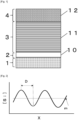
- Fig. 1 schematically illustrates a longitudinal section of a coating layer of a surface coated cutting tool according to one embodiment of the invention (a cross-section perpendicular to the surface when the minute irregularities on the surface of the tool substrate are ignored and treated as a smooth surface for an insert, or a cross section perpendicular to the axis for an axial tool such as a drill).
- the coating layer includes a lower layer (2), an intermediate layer (3), and an upper layer (4), in sequence, on a tool substrate (1).
- the lower layer (2), the intermediate layer (3), and the upper layer (4) are also referred to an A layer (10), a B layer (11), and a C layer (12), respectively, which will be described in detail.
- the coating layer has an average thickness, i.e., an average total thickness of the lower layer, intermediate layer, and upper layer in a range of 0.5 to 8.0 ⁇ m because a thickness below 0.5 ⁇ m does not lead to high wear resistance of the coating layer over long-term use whereas a thickness above 8.0 ⁇ m leads to abnormal damage, such as chipping, fracture, and separation of the upper layer.
- the coating layer has an average thickness in a range of 1.0 to 6.0 ⁇ m.
- the lower layer is an A layer having a predetermined composition (Al, Cr)N.
- Al contributes to improvements in high-temperature hardness and heat resistance
- Cr contributes to improvements in high-temperature strength and lubricity
- coexistence of Al and Cr contribute to improvements in oxidation resistance and wear resistance of the lower layer.
- the average composition of the A layer is expressed by the formula: (Al 1-x Cr x )N, x is in a range of 0.20 to 0.60.
- x is less than 0.20, the chipping resistance of the coating layer decreases due to a decrease in high-temperature strength of the lower layer, the hardness and thus wear resistance of the coating layer decreases due to formation of hexagonal crystal grains caused by an increase in relative Al content. If x is greater than 0.6, the lower layer does not exhibit sufficient high-temperature hardness and heat resistance caused by a decrease in relative Al content, resulting in a decrease in wear resistance of the coating layer.
- x ranges from 0.25 to 0.50.
- the lower layer or A layer has an average thickness in a range of 0.1 to 4.0 ⁇ m for the following reasons.
- the A layer has an average thickness less than 0.1 ⁇ m, the A layer does not sufficiently adhere to the tool substrate. If the A layer has an average thickness greater than 4.0 ⁇ m, the A layer has large internal distortion that causes abnormal damage such as chipping and separation between the A layer and the tool substrate to lose the function as an adhesive layer.
- the average thickness preferably ranges from 0.1 to 2.0 ⁇ m.
- the ratio of (Al, Cr) to N is to be 1:1.
- some products unavoidably (unintentionally) do not have a ratio of 1:1. This also holds for other composite nitrides described below.
- the intermediate layer or B layer is composed of (Al,Cr,Si)N with a predetermined texture.
- Cr improves the high-temperature strength and lubricancy of the intermediate layer, and the chipping resistance. Coexistence of Cr and Al contributes to improvements in high-temperature oxidation resistance and wear resistance of the intermediate layer.
- Si improves heat resistance and thermoplastic deformation resistance, and increases the lattice distortion of the intermediate layer at the same time to decrease the chipping resistance of the intermediate layer; hence, a repeated variation in Si level (concentration) is provided, as described below.
- the intermediate layer or B layer has an average thickness in a range of 0.1 to 4.0 ⁇ m.
- An average thickness less than 0.1 ⁇ m does not ensure sufficient wear resistance of the coating layer over long time periods.
- An average thickness greater than 4.0 ⁇ m accelerates abnormal damage, such as chipping, fracture, and separation of the coating layer.
- the intermediate layer or B layer preferably has an average thickness in a range of 0.1 to 2.0 ⁇ m.
- the average composition of the B layer is expressed by the formula: (Al 1-a-b Cr a Si b )N, a is 0.20 to 0.60 and b is 0.01 to 0.20 for the following reasons.
- a is less than 0.20, the chipping resistance of the coating layer decreases due to a decrease in high-temperature strength of the B layer, the hardness and thus wear resistance of the coating layer decreases due to formation of hexagonal crystal grains in the B layer caused by an increase in relative Al content. If a is greater than 0.6, the B layer does not exhibit sufficient high-temperature hardness and heat resistance caused by a decrease in relative Al content, resulting in a decrease in wear resistance of the coating layer. Preferably, a ranges from 0.25 to 0.50.
- b is less than 0.01, the B layer barely improves the heat resistance and thermoplastic deformation resistance. If b exceeds 0.20, the function of improving wear resistance decreases, and the lattice distortion of the B layer increases at the same time, resulting in a decrease in the toughness of the B layer itself. As a result, the chipping and fracture resistance of the coating layer decreases under high-load cutting conditions.
- the preferred range for b is from 0.01 to 0.15.
- a structure with a repeated variation in Si level is formed in the B layer in this embodiment.
- Fig. 2 shows a schematic diagram of a repeated variation in Si level ([Si]) on the vertical axis versus the position (X) perpendicular to the surface of the tool substrate on the horizontal axis.
- the drawing schematically shows an example of the repeated variation in Si level.
- local maxima have the same value and local minima also have the same value, and the intervals between adjacent local maxima and local minima are also the same.
- the repeated variation in Si level referred to in this specification and in the claims means the variation in Si level between the local maxima and local minima.
- the Si level should vary so that it alternates between local maxima and local minima in the direction perpendicular to the tool substrate surface, and the local maxima and local minima may be the same or different, and the interval (D) between adjacent local maxima and local minima may also be the same or different
- the average interval between adjacent local maxima and local minima in the direction perpendicular to the tool substrate surface of the Si level is controlled to be 1 to 100 nm for the following reasons: An average interval less than 1 nm leads to an abrupt variation in Si content generating large local lattice distortion, resulting in a decrease in chipping resistance. An average interval greater than 100 nm leads to generation of a wide area of high Si content, i.e., broad lattice distortion that works as a start point of chipping, resulting in a decrease in chipping resistance.
- the preferred average interval of the repeated variation ranges from 5 to 50 nm.
- the relation 1.0 ⁇ Si max /b ⁇ 2.0 holds where Si max is the average of local maxima of the concentrations of the Si component and b is an average content of Si in the composition, whereas the relation 0.0 ⁇ Si min /b ⁇ 1.0 holds where Si min is the average of local minima of the concentrations of the Si component.
- the ratio Si max /b of the average of the local maxima of the concentration of the Si component to b and the ratio Si min /b of the average of the local minima to b are determined for the following reasons: Although a Si max /b above 1.0 or a Si min /b below 1.0 contributes to a reduction in lattice distortion due to a repeated variation of Si level, a Si max /b above 2.0 leads to an abrupt variation in Si component due to a wide range of variations, resulting in a decrease in chipping resistance. Preferred ranges for Si max /b and Si min /b satisfy the relations 1.2 ⁇ Si max /b ⁇ 2.0 and 0.0 ⁇ Si min /b ⁇ 0.8.
- the average interval between a position giving a local maxima and the adjacent position giving a local minima of the Si level in the B layer with a repeated variation in Si level is determined as follow:
- the Si content is measured in a direction perpendicular to the tool substrate surface (layer thickness direction: described in "III. Measurement” below) in the longitudinal section of the tool substrate of the B layer, and the data is then graphed after known noise reduction.
- a straight line (m) is drawn across the curve showing the repeated variation in Si level.
- This straight line (m) is drawn such that the area of the region surrounded by the curve is equal on the upper side and the lower side of the straight line (m).
- the local maxima or local minima of the concentration of the Si component are determined for every area where the straight line (m) crosses the curve showing the repeated variation in Si level, and the intervals between the local maxima and the local minima are measured.
- the average interval of the repeated variation in Si level in the B layer is determined by averaging the observed values at multiple points.
- the averages of the local maxima Si max and the local minima Si min of the Si level are calculated by averaging the local maxima and local minima of the concentrations of the Si component measured at multiple points.
- the upper layer is a C layer having a given composition of (Ti,Si,W)N.
- the upper layer exhibits improvements in oxidation resistance and thermo-plastic deformation resistance due to Ti as the primary component and a Si component, as well as improvements in high-temperature strength and wear resistance of the coating layer due to a W component.
- the upper layer has an average thickness in a range of 0.1 to 4.0 ⁇ m to further improve chipping resistance, fracture resistance, and wear resistance of the coating layer under high-load cutting conditions.
- Preferred average thickness ranges from 0.1 to 2.0 ⁇ m.
- the average composition of the C layer is represented by the formula: (Ti 1- ⁇ - ⁇ Si ⁇ W ⁇ )N where ⁇ is in a range of 0.01 to 0.20 and ⁇ is in a range of 0.01 to 0.10.
- ⁇ is less than 0.01, the oxidation resistance and thermo-plastic deformation resistance of the C layer barely improves. If ⁇ exceeds 0.20, the lattice distortion increases, resulting in breakage of the C layer under high-load cutting conditions.
- ⁇ is less than 0.01, the strength of the C layer does not significantly increases at high temperature. If ⁇ exceeds 0.10, lattice distortion increases, resulting in a decrease in chipping resistance of the C layer under high-load cutting operations.
- the W level has a repeated variation with an average interval of 1 to 100 nm between adjacent local maxima and local minima in the direction perpendicular to the tool substrate surface, which satisfies the relation: 1.0 ⁇ W max / ⁇ ⁇ 2.0 where W max is the average of the local maxima of the W level and the relation: 0.0 ⁇ W min / ⁇ ⁇ 1.0 where W min is the average of the local minima of the W level, and ⁇ is the average composition of the C layer.
- 1 to 100 nm is as the average interval between adjacent local maxima and local minima in the direction perpendicular to the tool substrate surface is because an average interval of less than 1 nm leads to an abrupt variation in W content, resulting in large local lattice distortion in the C layer and decreased chipping resistance of the coating layer whereas an average interval exceeding 100 nm leads to a large W-rich area, i.e., a large area of high lattice distortion in the upper layer, accelerates chipping starting from this area, resulting in a decrease in chipping resistance of the coating layer.
- the average interval of a repeated variation preferably ranges from 5 nm to 50 nm
- the ratio W max / ⁇ of the average of the local maxima of W level to ⁇ , and the ratio W min / ⁇ of the average of the local minima of W level to ⁇ are determined in the above range for the following reasons: A ratio W max / ⁇ exceeding 1.0 and a ratio W min / ⁇ of less than 1.0 lead to a reduction in lattice distortion in the C layer due to a repeated variation in composition. In contrast, a ratio W max / ⁇ of greater than 2.0 leads to a large variation in composition and a steep variation in the W level. A ratio W max / ⁇ exceeding 2.0 leads to a large width of variable composition and decreased chipping resistance of the coating layer due to a steep variation in W level. Preferred ranges of the ratios W max / ⁇ and W min / ⁇ are represented by the relations: 1.2 ⁇ W max / ⁇ ⁇ 2.0 and 0.0 ⁇ W min / ⁇ ⁇ 0.8.
- the average intervals W max and W min can be determined as in the repeated variation in Si level described based on Fig. 2 .
- Si should be replaced by W in Fig. 2 .
- the crystal grains constituting the A, B, and C layers should preferably have a NaCl-type face-centered cubic structure.
- an unavoidable (unintended) amount of crystal grains having a crystal structure other than the NaCl-type face-centered cubic structure may also be present in industrial production.
- each layer included in the coating layer includes crystal grains having a rock-salt cubic crystal structure; a combined X-ray (200) diffraction peak derived from the A layer and the B layer has a full width at half maximum ranging from 0.2 degrees to 1.0 degrees; the intensity I AB200 of the (200) diffraction peak and the intensity I AB111 of the (111) diffraction peak are correlated by expression: 0.5 ⁇ I AB200 /IA B111 ⁇ 10.0; and the intensity I C200 of the (200) diffraction peak and the intensity I C111 of the (111) diffraction peak derived from the C layer are correlated by expression: 0.5 ⁇ I C200 /I C111 ⁇ 10.0.
- a full width of less than 0.2 degrees at half height of the X-ray diffraction peak intensity I AB200 indicates formation of coarse crystal grains that accelerate propagation of cracks through grain boundaries, resulting in decreased chipping resistance.
- a full width exceeding 1.0 degree at half height of the X-ray diffraction peak intensity I AB200 indicates formation of fine crystal grains that impairs sufficient crystallinity, resulting in a decrease in abrasion resistance. Setting the full width at half value in the above range achieves a small difference in lattice constants of the crystals constituting the A and B layers and small strain due to lattice mismatch at the interface between the A and B layers, resulting in improved chipping resistance.
- a ratio I AB200 /I AB111 of 0.5 or less indicates that the (111) plane orientation, which is the densest plane, is dominant, resulting in lower chipping resistance.
- a ratio I AB200 /I AB111 of 10.0 or greater indicates that orientation of the (200) plane is significantly dominant, resulting in lower wear resistance.
- a ratio I C200 /I C111 of 0.5 or less indicates that the (111) orientation, which is the densest plane, is dominant, resulting in lower chipping resistance.
- a ratio I C200 /I C111 of 10.0 or more indicates that the (200) orientation is significantly dominant, resulting in lower wear resistance.
- the combined X-ray diffraction peak derived from the A layer and the B layer indicates that the diffraction peaks from the A layer and the B layer overlap each other and the diffraction peak derived from the A layer or the B layer is not observed solely.
- cemented carbide WC-based cemented carbide, containing Co in addition to WC, and also containing carbonitrides of Ti, Ta, and Nb
- thermets primarily composed of, for example, TiC, TiN, or TiCN
- ceramics titanium carbide, silicon carbide, silicon nitride, aluminum nitride, or aluminum oxide
- cBN sinter cBN sinter
- diamond sinter diamond sinter.
- the tool substrate may have any shape, for example, the shape of an insert or a drill, usable as a cutting tool.
- the coated tool of this embodiment can be produced, for example, by the following PVD process.
- a tool substrate (26) is mounted on a turn table (25) under a nitrogen atmosphere in an arc ion plating (AIP) system shown in Figs. 5 and 6 ; and an arc discharge is generated between an Al-Cr alloy target (23) and an anode (20) to deposit a lower layer being an A layer with a specified average thickness on the surface of the spinning tool substrate.
- AIP arc ion plating
- the tool substrate (26) provided with the lower layer placed on the turn table (25) in the arc ion plating system is subjected to simultaneous deposition from an Al-Cr-Si alloy target (22) and an Al-Cr alloy target (23) to form an intermediate layer or B layer containing Si with a repeated variation in Si level.
- a repeated variation in Si level can be achieved by appropriate determination of the deposition conditions, such as rotation cycle of the turn table, nitrogen pressure and bias voltage during arc discharge, and temperature in the system; a coating layer of this embodiment can thereby be formed.
- a repeated variation in Si level with a single target are formed by the distribution of elements during deposition in the system. For example, an increase in nitrogen pressure causes a large difference in the mean free path for each element, resulting in ready formation of a repeated variation in Si level. If the tool substrate temperature is raised by an increase in the bias voltage or the temperature of the system in this case, atomic diffusion is more likely to occur in the coating layer, precluding a repeated variation in Si level.
- Use of a single target limits independent control of a repeated variation in Si level and the characteristics, such as crystallinity, of the coating layer.
- Simultaneous deposition from an Al-Cr-Si alloy target and an Al-Cr alloy target facilitates a repeated variation in Si level and control of the characteristics such as crystallinity to certainly form a coated layer of this embodiment.
- a tool substrate (26) having a surface provided with a lower layer and an intermediate layer is placed on the turn table (25) in the arc ion plating system and is subjected to simultaneous deposition using two Ti-Si-W alloy targets (21) having two different compositions to form a C layer having a repeated variation in W level.
- a repeated variation in W level can also be formed through adjustment of the deposition conditions with only Ti-Si-W alloy targets of the same composition, like a repeated variation in Si level in the B layer described above.
- the ratio I C200 /I C111 can be controlled within a predetermined range through adjustment of, for example, arc current, bias voltage, pressure of the reaction gas, and deposition temperature among the arc ion plating conditions for depositing the C layer.
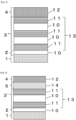
- Fig. 3 is a schematic longitudinal section of a coating layer of a surface coated cutting tool for another embodiment of the invention. The embodiment shown in Fig. 3 will now be described.
- the coating layer includes a lower layer (2), an intermediate layer (3'), and an upper layer (4) in sequence from the tool substrate (1) toward the surface of the tool, and the lower layer (2) is referred to an A layer (10) and the upper layer (4) is composed of a C layer (12), like the embodiment shown in Fig. 1 .
- the intermediate layer (3') consists of a D layer (13) including A layers (10) and B layers (11) alternatingly deposited.
- the number of A layers (10) and B layers (11) is not limited to that shown in Fig. 3 .
- the intermediate layer consists of layer D, which is an alternating layering of A layers and B layers.
- the average thickness of the layer D preferably ranges from 0.5 to 4.0 ⁇ m because an average thickness of less than 0.5 ⁇ m precludes sufficient wear resistance of the coating layer over a long period of time whereas an average layer thickness exceeding 4.0 ⁇ m accelerates abnormal damage, such as chipping, fracture, and separation.
- the average thicknesses of each of the A and B layers should preferably ranges from 0.1 to 1.5 ⁇ m.
- the layer closest to the tool substrate (on the lowest layer) and the layer closest to the tool surface (on the uppermost layer) are both B layers for the following reasons:
- the B layer formed closest to the tool substrate ensures high adhesion strength between the lower layer (A layer) and the intermediate layer (D layer) while the B layer formed closest to the surface of the tool improves the adhesion strength to the C layer, which is the upper layer, and ensures the chipping resistance of the coating layer in heavy-load cutting operations.
- any number of A and B layers can be deposited in the D layer and the number of deposited layers can be determined with proviso that the average thickness of each of the A and B layers in the D layer ranges from 0.1 to 1.5 ⁇ m and the thickness of the intermediate layer is 0.5 to 4.0 ⁇ m.
- the number of A layers and B layers are two to five, more specifically, a combination of two A layers and three B layers.
- crystal grains of the rock-salt cubic crystal structure and the XRD pattern are the same as described in the description of the embodiment shown in Fig. 1 .
- the material for and shape of the tool substrate are the same as those described in the description of the embodiment shown in Fig. 1 .
- a tool substrate (26) having the lower layer on the surface on a turn table (25) is subject to simultaneous deposition using an Al-Cr-Si alloy target (22) and an Al-Cr alloy target (23) in the arc ion plating system shown in Figs. 5 and 6 to deposit an intermediate layer or B layer having an alternatingly deposited structure with a repeated variation in Si level, and then is subject to deposition using the Al-Cr alloy target (23) to form an A layer with a predetermined thickness.
- This procedure is repeated to form alternatingly deposited B layers and A layers, with each B layer having a repeated variation in Si level.
- Fig. 4 is a schematic illustration of a longitudinal section of a coating layer of a surface coated cutting tool for yet another embodiment of the invention. This embodiment shown in Fig. 4 will now be described.
- the coating layer has a lower layer (2), an intermediate layer (3'), an upper layer (4), and an adhesive layer (5) between the intermediate layer (3') and the upper layer (4).
- the number of layers constituting the intermediate layer (3') should not be limited to that shown in the drawing.
- the adhesive layer is composed of an E layer between the intermediate layer (D layer) and the upper layer (C layer).
- the E layer is provided to enhance the adhesion between the D layer and the C layer.
- the E layer preferably has an average thickness in a range of 0.1 to 2.0 ⁇ m.
- An average thickness of the E layer of less than 0.1 ⁇ m cannot ensure sufficient adhesion between the C layer and the D layer, whereas an average thickness exceeding 2.0 ⁇ m leads to large lattice distortion in the E layer, resulting in a decrease in adhesiveness.
- the average composition of the E layer is represented by the formula: (Al 1-k-l-m-n Ti k Cr l S m W n )N, where k preferably ranges from 0.20 to 0.65, l preferably ranges from 0.10 to 0.35, m preferably ranges from above 0.00 to 0.15, and n preferably ranges from above 0.00 to 0.05.
- the ground for determining the average composition in this manner is as follows: Ti, which improves the high-temperature hardness and high-temperature strength of the E layer, does not provide sufficient high-temperature strength at a content of less than 0.20.
- the Al content is high, resulting in the formation of hexagonal crystals in the E layer, which precludes the function to improve the adhesion of the E layer.
- An Al content exceeding 0.65 leads to small contents of the other components and thus insufficient wear resistance of the coating layer.
- chromium which improves high-temperature strength and lubricating characteristics of the E layer, a Cr content of less than 0.10 leads to insufficient lubricating characteristics, whereas a Cr content of greater than 0.35 leads to small contents of the other components and thus insufficient wear resistance of the coating layer.
- a Si content of 0.00 does not provide sufficient oxidation resistance of the E layer or adhesion of the B layer to the C layer, whereas a Si content exceeding 0.15 increases lattice distortion in the E layer and thus decreases the adhesiveness.
- the adhesive layer preferably satisfies the relation: 1.0 ⁇ Si max(E) /m ⁇ 2.0, where Si max(E) represents the average of the local maxima of the Si levels in a repeated variation between adjoining local maxima and local minima with an interval between local maxima and local minima in a range of 1 to 100 nm, and the relation: 0.0 ⁇ Si min(E) /m ⁇ 1.0 where Si min(E) represents the average of the local minima of the Si levels.
- the repeated variation in the Si level is the same as that described with reference to Fig. 2 .
- the average interval between adjoining local maxima and local minima is preferably in a range of 1 to 100 nm for the following reasons: An average interval of less than 1 nm leads to steep variations in Si component that facilitates chipping of the coating layer and precludes adhesion between the C layer and the D layer in the E layer. An average interval exceeding 100 nm leads to expansion of a region with a high Si content, in other words, a region with large lattice distortion, resulting in ready chipping and unsatisfactory adhesive strength. A more preferred average interval in the repeated variation ranges from 5 to 50 nm.
- the ratio Si max(E) /m of the average local maxima of the Si level to m and the ratio Si min(E) /m of the average local minima of the Si level to m are determined as described above, for the following reasons: Si max(E) /m exceeding 2.0 leads to a steep repeated variation in Si level, resulting in a decrease in chipping resistance, although a combination of Si max(E) /m exceeding 1.0 and Si min(E) /M of less than 1.0 can produce a repeated variation in Si level.
- the crystal grains preferably have a NaCl-type face-centered cubic structure with respect to the crystal structure of the crystal grains.
- the E layer, the A layer, the B layer, and the D layer may contain an unavoidable (unintended) amount of crystal grains having a crystal structure other than the NaCl-type face-centered cubic structure.
- the material for and shape of the tool substrate are the same as described in the description of the embodiment shown in Fig. 1 .
- the tool substrate (26) with a lower layer and an intermediate layer formed on its surface on a turn table (25) in the arc ion plating system shown in Figs. 5 and 6 is subjected to simultaneous deposition using an Al-Cr-Si alloy target (22) and an Ti-Si-W alloy target (21) to form an adhesive layer or E layer containing Si with a repeated variation in Si level.
- the intermediate layer is a D layer, which is an alternating stack of A layers and B layers, in the embodiment shown in Fig. 4 , the intermediate layer may consist of only a B layer.
- the concentrations or levels of the components of each layer are determined by averaging values observed in a longitudinal cross-section of a sample by energy dispersive X-ray spectroscopy (EDS) of a scanning electron microscope (SEM) and a transmission electron microscope (TEM).
- EDS energy dispersive X-ray spectroscopy
- SEM scanning electron microscope
- TEM transmission electron microscope
- the surface of the tool substrate is defined as a reference line of the rough interface between the tool substrate and the coating layer in the observed image of the longitudinal section.
- elements are mapped by EDS on the longitudinal section, and the obtained map is subjected to known image processing.
- the interface between the lower layer and the tool substrate is determined by known image processing on the obtained elemental map, and the average line of the roughness curve of the interface between the lower layer and the tool substrate is obtained arithmetically, and is defined as the surface of the tool substrate.
- the direction perpendicular to the average line is defined by the direction of the thickness of the layer perpendicular to the tool substrate.
- a tool diameter sufficiently large in relation to the thickness of the coating layer has a flat interface between the coating layer and the tool substrate in the measured area.
- the surface of the tool substrate can thereby be determined by the same process.
- elemental mapping by EDS is performed on the longitudinal section of the coating layer in the cross-section perpendicular to the axial direction, and by performing known image processing on the obtained elemental map.
- the interface between the lower layer (A layer) and the tool substrate is determined, and the average line of the rough interface between the lower layer (A layer) and the tool substrate measured in this way is determined arithmetically, and this is used as the tool substrate surface.
- the direction perpendicular to this average line is the direction of the thickness of the layer perpendicular to the tool substrate.
- the area for measurement in the longitudinal section is determined so as to include the entire thickness of the coating layer. In consideration of the total thickness of the coating layer and the measurement accuracy of the thickness, it is preferred to observe and measure multiple fields of view (e.g., three fields of view) of about 10 ⁇ m ⁇ 10 ⁇ m.
- the average thickness is determined by averaging the thicknesses measured on multiple analytical lines for this layer.
- each of the A layer, B layer, C layer and E layer is identified to be a NaCl-type face-centered cubic structure by electron diffraction with a transmission electron microscope (TEM).
- TEM transmission electron microscope
- This example describes a coated tool provided with a coating layer including a lower layer (A layer), an intermediate layer (B layer), and an upper layer (C layer), as shown in Fig. 1 .
- a drill substrate was prepared as a tool substrate.
- Raw powders of Co, VC, TaC, NbC, Cr 3 C 2 , and WC each having an average grain diameter in a range of 0.5 to 5 ⁇ m were prepared. These powders were compounded into compositions shown in Table 1, and wax was added to the mixtures followed by wet mixing for 72 hours in a ball mill. The mixtures were then dried under reduced pressure and compacted under a pressure of 100 Mpa.
- the drill substrates 1 to 3 were subjected to the following procedures (a) to (e) for layer deposition in an arc ion plating system shown in Figs. 5 and 6 .
- An arc ion plating system shown in Figs. 5 and 6 is provided with an anode (20), a heater (24), a reaction gas inlet (27), an exhaust gas outlet (28), an arc power supply (29), and a bias power supply (30), in addition to the turn table (25) and the targets (21, 22, 23), which are described above.
- each C layer in Examples 1 to 5 and 7 was formed by the simultaneous deposition using two different Ti-Si-W alloy targets, and the C layer in Example 6 was formed by the deposition of a single Ti-Si-W alloy target and the control of deposition parameters to form a repeated variation in W level in each C layer.
- Coating layers each including a lower layer (A layer) and an intermediate layer (B layer) shown in Table 6 and an upper layer (C layer) shown in Table 7 of Examples 1 to 7 were prepared by Processes (a) to (e) above.
- the arc current, partial pressure of reactive nitrogen gas, bias voltage, and deposition temperature among deposition conditions for the A layer and B layer were adjusted to control the full width I AB200 /I AB111 values at half height of I AB200 of grains with a rock-salt cubic crystal structure in the intermediate layer by simultaneous deposition using an Al-Cr alloy target and an Al-Cr-Si alloy target.
- a coating layer including a lower layer (A layer), an intermediate layer (B layer) and an upper layer (C layer) was deposited on each of the drill substrates 1 to 3 as in Example 1 under the conditions 11 to 16 shown in Tables 4 and 5. Coating layers of Comparative examples 1 to 6 shown in Tables 8 and 9 were thereby prepared.
- Comparative Examples 1 to 5 differ from Examples in configuration of the intermediate layer (B layer) in this regard.
- the C layer of Comparative Examples 1 and 6 has a substantially uniform W content across the thickness of the C layer without a repeated variation in W level.
- the C layers in Comparative Examples 1 and 6 were formed by vapor deposition using a single Ti-Si-W alloy target in the same way as the C layer in Example 6, a large absolute values of the system temperature and bias voltage and a small nitrogen gas pressure created an environment where a repeated variation in W level were barely formed compared to Examples.
- the longitudinal cross sections of the coating layers of Examples 1 to 6 and Comparative Examples 1 to 6 were examined by scanning electron microscopy (SEM), transmission electron microscopy (TEM), and energy dispersive X-ray spectroscopy (EDS).
- SEM scanning electron microscopy
- TEM transmission electron microscopy
- EDS energy dispersive X-ray spectroscopy
- the B layer was further measured across the thickness of the layer by scanning electron microscopy (SEM), transmission electron microscopy (TEM), and energy dispersive X-ray analysis (EDS) to obtain composition distribution curves across the thickness of the layer.
- SEM scanning electron microscopy
- TEM transmission electron microscopy
- EDS energy dispersive X-ray analysis
- the average Si max of the local maxima of the Si level and the average Si min of the local minima of the Si level were obtained by smoothing the Si content in the composition distribution curve by moving average, which is noise elimination, and the average interval between the adjacent local maxima and local minima points of Si content was measured.
- the average W max of the local maxima of the W level at the points containing the local maxima of the W component and the average W min of the local minima of the W level at the points containing the local minima of the W component were obtained in the same way, and the intervals between adjacent W local maxima and W local minima were measured at multiple sites to obtain the average interval between the local maxima and local minima.
- X-ray diffraction was also performed on the entire A layer and B layer from a direction perpendicular to the surface of the tool substrate, and the full width at half maximum of the overall X-ray diffraction peak (overlapped X-ray diffraction peaks of the A layer and B layer) from the (200) plane was measured to calculate the ratio I AB200 /I AB111 from the intensities I AB200 and I AB111 of the overall X-ray diffraction peaks (overlapped X-ray diffraction peaks of the A layer and B layer).
- the C layer was also subjected to X-ray diffraction to measure the X-ray diffraction peak intensity I C200 of the 200 diffraction peak and the X-ray diffraction peak intensity I C111 of the 111 diffraction peak to calculate the ratio I C200 /I C111 .
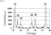
- Fig. 7 shows the results of X-ray diffraction (X-ray intensity on the vertical axis and angle on the horizontal axis) measured for the overall A layer and B layer in Example 6.
- the full width at half maximum of I AB200 is 0.5 (degrees), and the ratio I AB200 /I AB111 of I AB200 to I AB111 was 1.7.
- the ratio I C200 /I C111 of the hard coating layer consisting of the C layer was 0.9.
- Tables 6 and 7 show the full width at half maximum of I 200 , the ratio I AB200 /I AB111 , and the ratio I C200 /I C111 for Examples 1 to 7.
- Tables 8 and 9 show the full width at half maximum of I AB200 , the ratio I AB200 /I AB111 , and the ratio I C200 /I C111 for Comparative example tools 1 to 6.
- Table 2 Deposition condition of A and B layers Cathode (target electrode) Deposition Condition System temp.
- the number of holes drilled was counted until the flank wear width of the cutting edge surface reaches 0.3 mm or until the end of life due to chipping or fracture of the cutting edge or due to breakage, and the state of wear of the cutting edge was observed.
- the number of holes drilled was up to 1000 holes, and the flank wear width after 1000 holes drilling was measured for samples that did not reach the end of their service life.
- Drill substrates 1 to 3 made of WC-based cemented carbide fabricated in Example A were placed into an arc ion plating system shown in Figs. 5 and 6 .
- the lower layer (A layer) was formed under the conditions shown in Table 2 in the same manner as deposition processes (a) to (c) in Example A.
- Hard coating layers with lower layers (A layers) and intermediate layers (D layers consisting of alternating stacked structures of B and A layers) shown in Table 11 and upper layers (C layers) shown in Table 12 of Examples 11 to 17 were prepared by the above process.
- the D layer was also analyzed across the thickness by scanning electron microscopy (SEM), transmission electron microscopy (TEM), and energy dispersive X-ray spectroscopy (EDS) to determine the intervals between adjacent Si local maxima and Si local minima, the average Si max and Si min along the thickness of the layer, and the average interval between adjacent Si local maxima and Si local minima.
- SEM scanning electron microscopy
- TEM transmission electron microscopy
- EDS energy dispersive X-ray spectroscopy
- the average W max and W min were also calculated for the C layer, as well as the average interval between adjacent W local maxima and W local minima.
- the lower layer and the intermediate layer were subjected to X-ray diffractometry to measure the full width at half maximum of the 200 X-ray diffraction peak (the overlapped X-ray diffraction peak of the A layer and the B layer), and the ratio I AB200 /I AB111 was calculated from the intensities I AB200 and I AB111 of the overall X-ray diffraction peak (the overlapped X-ray diffraction peak of the A layer and the B layer).
- the C layer was also subjected to X-ray diffraction, and the 200 X-ray diffraction peak intensity I C200 and the 111 X-ray diffraction peak intensity I C111 were measured, to calculate the ratio I C200 /I C111 .
- Tables 11 and 12 shows the data determined through the above-mentioned process.
- the number of drilling operations was counted until the frank wear width of the cutting edge surface reaches 0.3 mm or until the end of life due to chipping, fracture, or breakage of the cutting edge.
- the number of holes drilled and the state of wear of the cutting edge were also observed.
- the number of holes drilled was up to 1000 holes. With the samples that did not reach the end of their service life, the flank wear width was measured after 1000 holes were formed.
- Drill substrates 1 to 3 made of WC-based cemented carbide fabricated in Example A were placed into an arc ion plating system shown in Fig. 5 and 6 , and a lower layer (A layer) was formed as in Example B under the conditions shown in Table 2, and an intermediate layer (D layer) was formed by the deposition processes (f) and (g) in Example B.
- drills of Examples 21 to 27 shown in Table 14 were fabricated where each drills included a hard coating layer consisting of a lower layer (A layer), an intermediate layer (D layer consisting of alternating B and A layers), an adhesive layer (E layer), and an upper layer (C layer) as shown in Table 11.
- the adhesive layer (E layer) has a structure having a repeated variation in Si level.
- the average interval Si max(E) of local maxima and the average interval Si min(E) of local minima of the Si content, and the average interval W max of local maxima and the average interval W min of local minima of the W content were obtained, as in Examples A and B.
- the full width at half maximum of the X-ray diffraction peak derived from the (111) plane and the full width at half maximum of the X-ray diffraction peak derived from the (200) plane were measured for the entire A layer and B layer as in Examples A and B, to calculate the ratio I AB200 /I AB111 .
- the ratio I C200 /I C111 of the C layer was also calculated.
- Table 15 shows the results of testing.
Landscapes
- Chemical & Material Sciences (AREA)
- Engineering & Computer Science (AREA)
- Mechanical Engineering (AREA)
- Chemical Kinetics & Catalysis (AREA)
- Materials Engineering (AREA)
- Metallurgy (AREA)
- Organic Chemistry (AREA)
- Inorganic Chemistry (AREA)
- Cutting Tools, Boring Holders, And Turrets (AREA)
- Physical Vapour Deposition (AREA)
- Drilling Tools (AREA)
Claims (4)
- Oberflächenbeschichtetes Schneidwerkzeug, umfassend: ein Werkzeugsubstrat [1] und eine Beschichtungsschicht auf einer Oberfläche des Werkzeugsubstrats; wobei1) die Beschichtungsschicht eine durchschnittliche Dicke im Bereich von 0,5 µm bis 8,0 µm hat und die Beschichtungsschicht eine untere Schicht [2], eine Zwischenschicht [3] und eine obere Schicht [4] in der Reihenfolge vom Werkzeugsubstrat zur Oberfläche des Werkzeugs umfasst;2) die untere Schicht eine durchschnittliche Dicke in einem Bereich von 0,1 µm bis 4,0 µm hat und eine A-Schicht [10] mit einer durchschnittlichen Zusammensetzung umfasst, die durch die Formel: (Al1-xCrx)N dargestellt wird, wobei x 0,20 bis 0,60 beträgt;3) die Zwischenschicht eine durchschnittliche Dicke in einem Bereich von 0,1 µm bis 4,0 µm hat und eine B-Schicht [11] mit einer durchschnittlichen Zusammensetzung umfasst, die durch die Formel: (Al1-a-bCraSib)N dargestellt wird, wobei a gleich 0,20 bis 0,60 und b gleich 0,01 bis 0,20 ist;4) die B-Schicht eine wiederholte Variation des Si-Spiegels mit einem durchschnittlichen Abstand von 1 nm bis 100 nm zwischen benachbarten lokalen Maxima und lokalen Minima in der Richtung senkrecht zur Oberfläche des Werkzeugsubstrats aufweist und die Beziehung: 1,0 < Simax/b ≤ 2,0, wobei Simax der Durchschnitt der lokalen Maxima des Si-Spiegels ist, und die Beziehung: 0,0 ≤ Simin/b < 1,0 erfüllt, wobei Simin der Mittelwert der lokalen Minima des Si-Spiegels ist;5) die obere Schicht eine durchschnittliche Dicke in einem Bereich von 0,1 µm bis 4,0 µm hat und eine C-Schicht [12] mit einer durchschnittlichen Zusammensetzung umfasst, dargestellt durch die Formel: (Ti1-α-βSiαWβ)N, wobei α 0,01 bis 0,20 und β 0,01 bis 0,10 ist; und6) die C-Schicht eine wiederholte Variation des W-Spiegels mit einem durchschnittlichen Abstand von 1 nm bis 100 nm zwischen benachbarten lokalen Maxima und lokalen Minima in der Richtung senkrecht zur Oberfläche des Werkzeugsubstrats aufweist und die Beziehung: 1,0 < Wmax/β ≤ 2,0, wobei Wmax der Durchschnitt der lokalen Maxima des W-Spiegels ist, und die Beziehung: 0,0 ≤ Wmin/β < 1,0 erfüllt, wobei Wmin der Mittelwert der lokalen Minima des W-Spiegels istwobei das durchschnittliche Intervall für Si und W wie im Teil "Beispiele" der Beschreibung beschrieben bestimmt wird.
- Oberflächenbeschichtetes Schneidwerkzeug nach Anspruch 1, wobei die Zwischenschicht eine D-Schicht [13] umfasst, die abwechselnd B-Schichten und A-Schichten umfasst, wobei die D-Schicht eine durchschnittliche Dicke in einem Bereich von 0,5 µm bis 4,0 µm aufweist und die D-Schicht mindestens zwei B-Schichten enthält.
- Oberflächenbeschichtetes Schneidwerkzeug nach Anspruch 1 oder 2, das ferner eine Haftschicht [5], die eine durchschnittliche Dicke im Bereich von 0,1 µm bis 2,0 µm aufweist, und eine E-Schicht [14] mit einer durch die Formel: (Al1-k-l-m-nTikCrlSimWn)N dargestellten Zusammensetzung umfasst, wobei k 0,20 bis 0,65, l 0,10 bis 0,35, m mehr als 0,00 bis 0,15 und n mehr als 0,00 bis 0,05 beträgt; wobei
die E-Schicht eine wiederholte Variation des Si-Spiegels mit einem durchschnittlichen Abstand von 1 nm bis 100 nm zwischen benachbarten lokalen Maxima und lokalen Minima aufweist und die Beziehung: 1,0 < Simax(E)/m ≤ 2,0, wobei Simax(E) der Durchschnitt der lokalen Maxima des Si-Spiegels ist, und die Beziehung: 0,0 ≤ Simin(E)/b < 1,0 erfüllt, wobei Simin(E) der Mittelwert der lokalen Minima des Si-Spiegels ist. - Oberflächenbeschichtetes Schneidwerkzeug nach einem der Ansprüche 1 bis 3, wobeijede in der Überzugsschicht enthaltene Schicht Kristallkörner mit einer kubischen Steinsalzkristallstruktur enthält;ein kombinierter Röntgenbeugungspeak (200), der von der A-Schicht und der B-Schicht stammt, eine Halbwertsbreite von 0,2 Grad bis 1,0 Grad hat;die Intensität IAB200 des (200)-Beugungspeaks und die Intensität IAB111 des (111)-Beugungspeaks durch den Ausdruck: 0,5 < IAB200/IAB111 < 10,0 korrelieren; unddie Intensität IC200 des (200)-Beugungspeaks und die Intensität IC111 des (111)-Beugungspeaks, jeweils von der C-Schicht stammend, durch den Ausdruck: 0,5 < IC200/IC111 < 10,0 korrelieren.
Applications Claiming Priority (2)
| Application Number | Priority Date | Filing Date | Title |
|---|---|---|---|
| JP2020059802 | 2020-03-30 | ||
| PCT/JP2021/010128 WO2021200042A1 (ja) | 2020-03-30 | 2021-03-12 | 表面被覆切削工具 |
Publications (3)
| Publication Number | Publication Date |
|---|---|
| EP4129541A1 EP4129541A1 (de) | 2023-02-08 |
| EP4129541A4 EP4129541A4 (de) | 2024-04-24 |
| EP4129541B1 true EP4129541B1 (de) | 2025-02-19 |
Family
ID=77927230
Family Applications (1)
| Application Number | Title | Priority Date | Filing Date |
|---|---|---|---|
| EP21782187.5A Active EP4129541B1 (de) | 2020-03-30 | 2021-03-12 | Oberflächenbeschichtetes schneidwerkzeug |
Country Status (5)
| Country | Link |
|---|---|
| US (1) | US12157171B2 (de) |
| EP (1) | EP4129541B1 (de) |
| JP (1) | JP7530580B2 (de) |
| CN (1) | CN115335166B (de) |
| WO (1) | WO2021200042A1 (de) |
Families Citing this family (2)
| Publication number | Priority date | Publication date | Assignee | Title |
|---|---|---|---|---|
| US20240043344A1 (en) * | 2020-12-22 | 2024-02-08 | Mitsubishi Materials Corporation | Surface coated cutting tool |
| JPWO2024185311A1 (de) * | 2023-03-06 | 2024-09-12 |
Family Cites Families (15)
| Publication number | Priority date | Publication date | Assignee | Title |
|---|---|---|---|---|
| US7537822B2 (en) * | 2005-05-26 | 2009-05-26 | Hitachi Tool Engineering, Ltd. | Hard-coated member |
| JP2008049454A (ja) | 2006-08-25 | 2008-03-06 | Mitsubishi Materials Corp | 硬質被覆層がすぐれた耐チッピング性と耐摩耗性を発揮する表面被覆切削工具 |
| JP2008173701A (ja) | 2007-01-17 | 2008-07-31 | Mitsubishi Materials Corp | 高速切削加工で硬質被覆層がすぐれた耐摩耗性を発揮する表面被覆切削工具 |
| JP2009039838A (ja) * | 2007-08-10 | 2009-02-26 | Mitsubishi Materials Corp | 表面被覆切削工具 |
| JP5087427B2 (ja) | 2008-02-28 | 2012-12-05 | ユニオンツール株式会社 | 切削工具用硬質皮膜 |
| JP2010137348A (ja) * | 2008-12-15 | 2010-06-24 | Mitsubishi Materials Corp | 硬質被覆層がすぐれた耐欠損性及び耐摩耗性を発揮する表面被覆切削工具 |
| JP5303816B2 (ja) | 2009-10-01 | 2013-10-02 | 日立ツール株式会社 | 硬質皮膜被覆工具 |
| JP5376375B2 (ja) | 2010-02-12 | 2013-12-25 | 住友電工ハードメタル株式会社 | 表面被覆切削工具 |
| JP2012045650A (ja) | 2010-08-25 | 2012-03-08 | Hitachi Tool Engineering Ltd | 硬質皮膜被覆切削工具 |
| JP2017080879A (ja) * | 2015-10-28 | 2017-05-18 | 三菱マテリアル株式会社 | 表面被覆切削工具 |
| US11014167B2 (en) | 2016-08-01 | 2021-05-25 | Mitsubishi Materials Corporation | Multilayer hard film-coated cutting tool |
| JP2018094670A (ja) * | 2016-12-13 | 2018-06-21 | 三菱マテリアル株式会社 | 耐摩耗性と耐欠損性を両立した表面被覆立方晶窒化ホウ素焼結体工具 |
| JP7083448B2 (ja) * | 2017-01-07 | 2022-06-13 | 株式会社タンガロイ | 被覆切削工具 |
| JP7138006B2 (ja) | 2018-10-10 | 2022-09-15 | Toyo Tire株式会社 | ゴム組成物の製造方法およびタイヤの製造方法 |
| JP7216914B2 (ja) | 2019-03-12 | 2023-02-02 | 三菱マテリアル株式会社 | 高負荷切削加工においてすぐれた耐チッピング性、耐摩耗性を発揮する表面被覆切削工具 |
-
2021
- 2021-03-12 US US17/913,919 patent/US12157171B2/en active Active
- 2021-03-12 EP EP21782187.5A patent/EP4129541B1/de active Active
- 2021-03-12 JP JP2022511773A patent/JP7530580B2/ja active Active
- 2021-03-12 WO PCT/JP2021/010128 patent/WO2021200042A1/ja not_active Ceased
- 2021-03-12 CN CN202180024545.4A patent/CN115335166B/zh active Active
Also Published As
| Publication number | Publication date |
|---|---|
| US12157171B2 (en) | 2024-12-03 |
| JP7530580B2 (ja) | 2024-08-08 |
| CN115335166A (zh) | 2022-11-11 |
| WO2021200042A1 (ja) | 2021-10-07 |
| JPWO2021200042A1 (de) | 2021-10-07 |
| EP4129541A4 (de) | 2024-04-24 |
| US20230119858A1 (en) | 2023-04-20 |
| CN115335166B (zh) | 2025-07-25 |
| EP4129541A1 (de) | 2023-02-08 |
Similar Documents
| Publication | Publication Date | Title |
|---|---|---|
| EP3369505B1 (de) | Oberflächenbeschichtetes schneidwerkzeug mit einer harten beschichtung mit ausgezeichneter spanbeständigkeit und herstellungsverfahren dafür | |
| EP3225337B1 (de) | Oberflächenbeschichtetes schneidwerkzeug mit hervorragender schlagbeständigkeit und verschleissfestigkeit | |
| EP3427872B1 (de) | Oberflächenbeschichtetes kubisches bornitrid-sinterwerkzeug | |
| US12203160B2 (en) | Surface-coated cutting tool | |
| US11014167B2 (en) | Multilayer hard film-coated cutting tool | |
| EP2962793A1 (de) | Schneidewerkzeug | |
| JP2021126738A (ja) | 強断続切削加工においてすぐれた耐チッピング性、耐摩耗性を発揮する表面被覆切削工具 | |
| EP3395484B1 (de) | Oberflächenbeschichtetes kubisches bornitrid-sinterkompaktwerkzeug | |
| US10710168B2 (en) | Surface-coated cutting tool in which hard coating layer exhibits excellent chipping resistance | |
| US12303982B2 (en) | Surface-coated cutting tool | |
| EP4129541B1 (de) | Oberflächenbeschichtetes schneidwerkzeug | |
| JP2017109254A (ja) | 耐チッピング性、耐摩耗性にすぐれた表面被覆切削工具 | |
| EP3219420B1 (de) | Oberflächenbeschichtetes schneidwerkzeug | |
| EP4295978A1 (de) | Oberflächenbeschichtetes schneidwerkzeug | |
| JP7755797B2 (ja) | 表面被覆切削工具 | |
| JP2020142312A (ja) | 表面被覆切削工具 | |
| WO2022196555A1 (ja) | 表面被覆切削工具 | |
| EP4464441A1 (de) | Oberflächenbeschichtetes schneidwerkzeug | |
| JP7794294B2 (ja) | 表面被覆切削工具 | |
| EP4667143A1 (de) | Oberflächenbeschichtetes schneidwerkzeug | |
| JP7570599B2 (ja) | 表面被覆切削工具 | |
| JP2025120620A (ja) | 表面被覆切削工具 | |
| WO2025169905A1 (ja) | 表面被覆切削工具 | |
| JP2026010801A (ja) | 表面被覆切削工具 | |
| JP2025120619A (ja) | 表面被覆切削工具 |
Legal Events
| Date | Code | Title | Description |
|---|---|---|---|
| STAA | Information on the status of an ep patent application or granted ep patent |
Free format text: STATUS: THE INTERNATIONAL PUBLICATION HAS BEEN MADE |
|
| PUAI | Public reference made under article 153(3) epc to a published international application that has entered the european phase |
Free format text: ORIGINAL CODE: 0009012 |
|
| STAA | Information on the status of an ep patent application or granted ep patent |
Free format text: STATUS: REQUEST FOR EXAMINATION WAS MADE |
|
| 17P | Request for examination filed |
Effective date: 20221010 |
|
| AK | Designated contracting states |
Kind code of ref document: A1 Designated state(s): AL AT BE BG CH CY CZ DE DK EE ES FI FR GB GR HR HU IE IS IT LI LT LU LV MC MK MT NL NO PL PT RO RS SE SI SK SM TR |
|
| DAV | Request for validation of the european patent (deleted) | ||
| DAX | Request for extension of the european patent (deleted) | ||
| REG | Reference to a national code |
Ref country code: DE Ref legal event code: R079 Free format text: PREVIOUS MAIN CLASS: B23B0027140000 Ipc: C23C0014060000 Ref document number: 602021026440 Country of ref document: DE |
|
| A4 | Supplementary search report drawn up and despatched |
Effective date: 20240321 |
|
| RIC1 | Information provided on ipc code assigned before grant |
Ipc: B23B 51/00 20060101ALN20240315BHEP Ipc: C23C 30/00 20060101ALI20240315BHEP Ipc: C23C 28/00 20060101ALI20240315BHEP Ipc: C23C 28/04 20060101ALI20240315BHEP Ipc: C23C 14/32 20060101ALI20240315BHEP Ipc: C23C 14/06 20060101AFI20240315BHEP |
|
| GRAP | Despatch of communication of intention to grant a patent |
Free format text: ORIGINAL CODE: EPIDOSNIGR1 |
|
| STAA | Information on the status of an ep patent application or granted ep patent |
Free format text: STATUS: GRANT OF PATENT IS INTENDED |
|
| RIC1 | Information provided on ipc code assigned before grant |
Ipc: B23B 51/00 20060101ALN20241028BHEP Ipc: C23C 30/00 20060101ALI20241028BHEP Ipc: C23C 28/00 20060101ALI20241028BHEP Ipc: C23C 28/04 20060101ALI20241028BHEP Ipc: C23C 14/32 20060101ALI20241028BHEP Ipc: C23C 14/06 20060101AFI20241028BHEP |
|
| RIC1 | Information provided on ipc code assigned before grant |
Ipc: B23B 51/00 20060101ALN20241101BHEP Ipc: C23C 30/00 20060101ALI20241101BHEP Ipc: C23C 28/00 20060101ALI20241101BHEP Ipc: C23C 28/04 20060101ALI20241101BHEP Ipc: C23C 14/32 20060101ALI20241101BHEP Ipc: C23C 14/06 20060101AFI20241101BHEP |
|
| INTG | Intention to grant announced |
Effective date: 20241115 |
|
| GRAS | Grant fee paid |
Free format text: ORIGINAL CODE: EPIDOSNIGR3 |
|
| GRAA | (expected) grant |
Free format text: ORIGINAL CODE: 0009210 |
|
| STAA | Information on the status of an ep patent application or granted ep patent |
Free format text: STATUS: THE PATENT HAS BEEN GRANTED |
|
| AK | Designated contracting states |
Kind code of ref document: B1 Designated state(s): AL AT BE BG CH CY CZ DE DK EE ES FI FR GB GR HR HU IE IS IT LI LT LU LV MC MK MT NL NO PL PT RO RS SE SI SK SM TR |
|
| REG | Reference to a national code |
Ref country code: GB Ref legal event code: FG4D |
|
| REG | Reference to a national code |
Ref country code: CH Ref legal event code: EP |
|
| REG | Reference to a national code |
Ref country code: DE Ref legal event code: R096 Ref document number: 602021026440 Country of ref document: DE |
|
| REG | Reference to a national code |
Ref country code: IE Ref legal event code: FG4D |
|
| PGFP | Annual fee paid to national office [announced via postgrant information from national office to epo] |
Ref country code: AT Payment date: 20250417 Year of fee payment: 5 |
|
| REG | Reference to a national code |
Ref country code: NL Ref legal event code: MP Effective date: 20250219 |
|
| PG25 | Lapsed in a contracting state [announced via postgrant information from national office to epo] |
Ref country code: RS Free format text: LAPSE BECAUSE OF FAILURE TO SUBMIT A TRANSLATION OF THE DESCRIPTION OR TO PAY THE FEE WITHIN THE PRESCRIBED TIME-LIMIT Effective date: 20250519 |
|
| PG25 | Lapsed in a contracting state [announced via postgrant information from national office to epo] |
Ref country code: FI Free format text: LAPSE BECAUSE OF FAILURE TO SUBMIT A TRANSLATION OF THE DESCRIPTION OR TO PAY THE FEE WITHIN THE PRESCRIBED TIME-LIMIT Effective date: 20250219 |
|
| PG25 | Lapsed in a contracting state [announced via postgrant information from national office to epo] |
Ref country code: PL Free format text: LAPSE BECAUSE OF FAILURE TO SUBMIT A TRANSLATION OF THE DESCRIPTION OR TO PAY THE FEE WITHIN THE PRESCRIBED TIME-LIMIT Effective date: 20250219 |
|
| PG25 | Lapsed in a contracting state [announced via postgrant information from national office to epo] |
Ref country code: ES Free format text: LAPSE BECAUSE OF FAILURE TO SUBMIT A TRANSLATION OF THE DESCRIPTION OR TO PAY THE FEE WITHIN THE PRESCRIBED TIME-LIMIT Effective date: 20250219 |
|
| REG | Reference to a national code |
Ref country code: LT Ref legal event code: MG9D |
|
| PG25 | Lapsed in a contracting state [announced via postgrant information from national office to epo] |
Ref country code: NO Free format text: LAPSE BECAUSE OF FAILURE TO SUBMIT A TRANSLATION OF THE DESCRIPTION OR TO PAY THE FEE WITHIN THE PRESCRIBED TIME-LIMIT Effective date: 20250519 Ref country code: IS Free format text: LAPSE BECAUSE OF FAILURE TO SUBMIT A TRANSLATION OF THE DESCRIPTION OR TO PAY THE FEE WITHIN THE PRESCRIBED TIME-LIMIT Effective date: 20250619 |
|
| PG25 | Lapsed in a contracting state [announced via postgrant information from national office to epo] |
Ref country code: NL Free format text: LAPSE BECAUSE OF FAILURE TO SUBMIT A TRANSLATION OF THE DESCRIPTION OR TO PAY THE FEE WITHIN THE PRESCRIBED TIME-LIMIT Effective date: 20250219 |
|
| PG25 | Lapsed in a contracting state [announced via postgrant information from national office to epo] |
Ref country code: HR Free format text: LAPSE BECAUSE OF FAILURE TO SUBMIT A TRANSLATION OF THE DESCRIPTION OR TO PAY THE FEE WITHIN THE PRESCRIBED TIME-LIMIT Effective date: 20250219 |
|
| PG25 | Lapsed in a contracting state [announced via postgrant information from national office to epo] |
Ref country code: PT Free format text: LAPSE BECAUSE OF FAILURE TO SUBMIT A TRANSLATION OF THE DESCRIPTION OR TO PAY THE FEE WITHIN THE PRESCRIBED TIME-LIMIT Effective date: 20250620 Ref country code: LV Free format text: LAPSE BECAUSE OF FAILURE TO SUBMIT A TRANSLATION OF THE DESCRIPTION OR TO PAY THE FEE WITHIN THE PRESCRIBED TIME-LIMIT Effective date: 20250219 |
|
| PG25 | Lapsed in a contracting state [announced via postgrant information from national office to epo] |
Ref country code: GR Free format text: LAPSE BECAUSE OF FAILURE TO SUBMIT A TRANSLATION OF THE DESCRIPTION OR TO PAY THE FEE WITHIN THE PRESCRIBED TIME-LIMIT Effective date: 20250520 Ref country code: BG Free format text: LAPSE BECAUSE OF FAILURE TO SUBMIT A TRANSLATION OF THE DESCRIPTION OR TO PAY THE FEE WITHIN THE PRESCRIBED TIME-LIMIT Effective date: 20250219 |
|
| REG | Reference to a national code |
Ref country code: AT Ref legal event code: MK05 Ref document number: 1768348 Country of ref document: AT Kind code of ref document: T Effective date: 20250219 |
|
| PG25 | Lapsed in a contracting state [announced via postgrant information from national office to epo] |
Ref country code: SE Free format text: LAPSE BECAUSE OF FAILURE TO SUBMIT A TRANSLATION OF THE DESCRIPTION OR TO PAY THE FEE WITHIN THE PRESCRIBED TIME-LIMIT Effective date: 20250219 |
|
| PG25 | Lapsed in a contracting state [announced via postgrant information from national office to epo] |
Ref country code: SM Free format text: LAPSE BECAUSE OF FAILURE TO SUBMIT A TRANSLATION OF THE DESCRIPTION OR TO PAY THE FEE WITHIN THE PRESCRIBED TIME-LIMIT Effective date: 20250219 |
|
| PG25 | Lapsed in a contracting state [announced via postgrant information from national office to epo] |
Ref country code: DK Free format text: LAPSE BECAUSE OF FAILURE TO SUBMIT A TRANSLATION OF THE DESCRIPTION OR TO PAY THE FEE WITHIN THE PRESCRIBED TIME-LIMIT Effective date: 20250219 |
|
| PG25 | Lapsed in a contracting state [announced via postgrant information from national office to epo] |
Ref country code: IT Free format text: LAPSE BECAUSE OF FAILURE TO SUBMIT A TRANSLATION OF THE DESCRIPTION OR TO PAY THE FEE WITHIN THE PRESCRIBED TIME-LIMIT Effective date: 20250219 |
|
| PG25 | Lapsed in a contracting state [announced via postgrant information from national office to epo] |
Ref country code: AT Free format text: LAPSE BECAUSE OF FAILURE TO SUBMIT A TRANSLATION OF THE DESCRIPTION OR TO PAY THE FEE WITHIN THE PRESCRIBED TIME-LIMIT Effective date: 20250219 |
|
| PG25 | Lapsed in a contracting state [announced via postgrant information from national office to epo] |
Ref country code: EE Free format text: LAPSE BECAUSE OF FAILURE TO SUBMIT A TRANSLATION OF THE DESCRIPTION OR TO PAY THE FEE WITHIN THE PRESCRIBED TIME-LIMIT Effective date: 20250219 Ref country code: CZ Free format text: LAPSE BECAUSE OF FAILURE TO SUBMIT A TRANSLATION OF THE DESCRIPTION OR TO PAY THE FEE WITHIN THE PRESCRIBED TIME-LIMIT Effective date: 20250219 |
|
| REG | Reference to a national code |
Ref country code: CH Ref legal event code: H13 Free format text: ST27 STATUS EVENT CODE: U-0-0-H10-H13 (AS PROVIDED BY THE NATIONAL OFFICE) Effective date: 20251023 |
|
| PG25 | Lapsed in a contracting state [announced via postgrant information from national office to epo] |
Ref country code: RO Free format text: LAPSE BECAUSE OF FAILURE TO SUBMIT A TRANSLATION OF THE DESCRIPTION OR TO PAY THE FEE WITHIN THE PRESCRIBED TIME-LIMIT Effective date: 20250219 |
|
| PG25 | Lapsed in a contracting state [announced via postgrant information from national office to epo] |
Ref country code: SK Free format text: LAPSE BECAUSE OF FAILURE TO SUBMIT A TRANSLATION OF THE DESCRIPTION OR TO PAY THE FEE WITHIN THE PRESCRIBED TIME-LIMIT Effective date: 20250219 |
|
| PG25 | Lapsed in a contracting state [announced via postgrant information from national office to epo] |
Ref country code: LU Free format text: LAPSE BECAUSE OF NON-PAYMENT OF DUE FEES Effective date: 20250312 |
|
| REG | Reference to a national code |
Ref country code: DE Ref legal event code: R097 Ref document number: 602021026440 Country of ref document: DE |
|
| REG | Reference to a national code |
Ref country code: BE Ref legal event code: MM Effective date: 20250331 |
|
| PG25 | Lapsed in a contracting state [announced via postgrant information from national office to epo] |
Ref country code: MC Free format text: LAPSE BECAUSE OF FAILURE TO SUBMIT A TRANSLATION OF THE DESCRIPTION OR TO PAY THE FEE WITHIN THE PRESCRIBED TIME-LIMIT Effective date: 20250219 |
|
| PLBE | No opposition filed within time limit |
Free format text: ORIGINAL CODE: 0009261 |
|
| STAA | Information on the status of an ep patent application or granted ep patent |
Free format text: STATUS: NO OPPOSITION FILED WITHIN TIME LIMIT |
|
| PG25 | Lapsed in a contracting state [announced via postgrant information from national office to epo] |
Ref country code: FR Free format text: LAPSE BECAUSE OF NON-PAYMENT OF DUE FEES Effective date: 20250419 |
|
| PG25 | Lapsed in a contracting state [announced via postgrant information from national office to epo] |
Ref country code: BE Free format text: LAPSE BECAUSE OF NON-PAYMENT OF DUE FEES Effective date: 20250331 |
|
| PG25 | Lapsed in a contracting state [announced via postgrant information from national office to epo] |
Ref country code: CH Free format text: LAPSE BECAUSE OF NON-PAYMENT OF DUE FEES Effective date: 20250331 |
|
| PG25 | Lapsed in a contracting state [announced via postgrant information from national office to epo] |
Ref country code: IE Free format text: LAPSE BECAUSE OF NON-PAYMENT OF DUE FEES Effective date: 20250312 |
|
| 26N | No opposition filed |
Effective date: 20251120 |
|
| GBPC | Gb: european patent ceased through non-payment of renewal fee |
Effective date: 20250519 |
|
| PG25 | Lapsed in a contracting state [announced via postgrant information from national office to epo] |
Ref country code: GB Free format text: LAPSE BECAUSE OF NON-PAYMENT OF DUE FEES Effective date: 20250519 |
|
| PGFP | Annual fee paid to national office [announced via postgrant information from national office to epo] |
Ref country code: DE Payment date: 20260319 Year of fee payment: 6 |