EP4120342A2 - Halbleiterbauelemente mit eingebauten pgs zur unterdrückung von kopplungsgeräuschen - Google Patents
Halbleiterbauelemente mit eingebauten pgs zur unterdrückung von kopplungsgeräuschen Download PDFInfo
- Publication number
- EP4120342A2 EP4120342A2 EP22183589.5A EP22183589A EP4120342A2 EP 4120342 A2 EP4120342 A2 EP 4120342A2 EP 22183589 A EP22183589 A EP 22183589A EP 4120342 A2 EP4120342 A2 EP 4120342A2
- Authority
- EP
- European Patent Office
- Prior art keywords
- shielding structure
- semiconductor device
- package
- semiconductor
- pgs
- Prior art date
- Legal status (The legal status is an assumption and is not a legal conclusion. Google has not performed a legal analysis and makes no representation as to the accuracy of the status listed.)
- Pending
Links
Images



Classifications
-
- H—ELECTRICITY
- H10—SEMICONDUCTOR DEVICES; ELECTRIC SOLID-STATE DEVICES NOT OTHERWISE PROVIDED FOR
- H10W—GENERIC PACKAGES, INTERCONNECTIONS, CONNECTORS OR OTHER CONSTRUCTIONAL DETAILS OF DEVICES COVERED BY CLASS H10
- H10W42/00—Arrangements for protection of devices
-
- H—ELECTRICITY
- H10—SEMICONDUCTOR DEVICES; ELECTRIC SOLID-STATE DEVICES NOT OTHERWISE PROVIDED FOR
- H10W—GENERIC PACKAGES, INTERCONNECTIONS, CONNECTORS OR OTHER CONSTRUCTIONAL DETAILS OF DEVICES COVERED BY CLASS H10
- H10W20/00—Interconnections in chips, wafers or substrates
- H10W20/40—Interconnections external to wafers or substrates, e.g. back-end-of-line [BEOL] metallisations or vias connecting to gate electrodes
- H10W20/41—Interconnections external to wafers or substrates, e.g. back-end-of-line [BEOL] metallisations or vias connecting to gate electrodes characterised by their conductive parts
- H10W20/423—Shielding layers
-
- H—ELECTRICITY
- H10—SEMICONDUCTOR DEVICES; ELECTRIC SOLID-STATE DEVICES NOT OTHERWISE PROVIDED FOR
- H10W—GENERIC PACKAGES, INTERCONNECTIONS, CONNECTORS OR OTHER CONSTRUCTIONAL DETAILS OF DEVICES COVERED BY CLASS H10
- H10W20/00—Interconnections in chips, wafers or substrates
- H10W20/40—Interconnections external to wafers or substrates, e.g. back-end-of-line [BEOL] metallisations or vias connecting to gate electrodes
- H10W20/497—Inductive arrangements or effects of, or between, wiring layers
-
- H—ELECTRICITY
- H10—SEMICONDUCTOR DEVICES; ELECTRIC SOLID-STATE DEVICES NOT OTHERWISE PROVIDED FOR
- H10W—GENERIC PACKAGES, INTERCONNECTIONS, CONNECTORS OR OTHER CONSTRUCTIONAL DETAILS OF DEVICES COVERED BY CLASS H10
- H10W42/00—Arrangements for protection of devices
- H10W42/20—Arrangements for protection of devices protecting against electromagnetic or particle radiation, e.g. light, X-rays, gamma-rays or electrons
-
- H—ELECTRICITY
- H10—SEMICONDUCTOR DEVICES; ELECTRIC SOLID-STATE DEVICES NOT OTHERWISE PROVIDED FOR
- H10W—GENERIC PACKAGES, INTERCONNECTIONS, CONNECTORS OR OTHER CONSTRUCTIONAL DETAILS OF DEVICES COVERED BY CLASS H10
- H10W42/00—Arrangements for protection of devices
- H10W42/20—Arrangements for protection of devices protecting against electromagnetic or particle radiation, e.g. light, X-rays, gamma-rays or electrons
- H10W42/261—Arrangements for protection of devices protecting against electromagnetic or particle radiation, e.g. light, X-rays, gamma-rays or electrons characterised by their shapes or dispositions
- H10W42/267—Patterned shielding planes
-
- H—ELECTRICITY
- H10—SEMICONDUCTOR DEVICES; ELECTRIC SOLID-STATE DEVICES NOT OTHERWISE PROVIDED FOR
- H10W—GENERIC PACKAGES, INTERCONNECTIONS, CONNECTORS OR OTHER CONSTRUCTIONAL DETAILS OF DEVICES COVERED BY CLASS H10
- H10W42/00—Arrangements for protection of devices
- H10W42/60—Arrangements for protection of devices protecting against electrostatic charges or discharges, e.g. Faraday shields
-
- H—ELECTRICITY
- H10—SEMICONDUCTOR DEVICES; ELECTRIC SOLID-STATE DEVICES NOT OTHERWISE PROVIDED FOR
- H10W—GENERIC PACKAGES, INTERCONNECTIONS, CONNECTORS OR OTHER CONSTRUCTIONAL DETAILS OF DEVICES COVERED BY CLASS H10
- H10W70/00—Package substrates; Interposers; Redistribution layers [RDL]
- H10W70/60—Insulating or insulated package substrates; Interposers; Redistribution layers
- H10W70/62—Insulating or insulated package substrates; Interposers; Redistribution layers characterised by their interconnections
- H10W70/65—Shapes or dispositions of interconnections
-
- H—ELECTRICITY
- H10—SEMICONDUCTOR DEVICES; ELECTRIC SOLID-STATE DEVICES NOT OTHERWISE PROVIDED FOR
- H10W—GENERIC PACKAGES, INTERCONNECTIONS, CONNECTORS OR OTHER CONSTRUCTIONAL DETAILS OF DEVICES COVERED BY CLASS H10
- H10W70/00—Package substrates; Interposers; Redistribution layers [RDL]
- H10W70/60—Insulating or insulated package substrates; Interposers; Redistribution layers
- H10W70/67—Insulating or insulated package substrates; Interposers; Redistribution layers characterised by their insulating layers or insulating parts
- H10W70/68—Shapes or dispositions thereof
- H10W70/685—Shapes or dispositions thereof comprising multiple insulating layers
-
- H—ELECTRICITY
- H10—SEMICONDUCTOR DEVICES; ELECTRIC SOLID-STATE DEVICES NOT OTHERWISE PROVIDED FOR
- H10W—GENERIC PACKAGES, INTERCONNECTIONS, CONNECTORS OR OTHER CONSTRUCTIONAL DETAILS OF DEVICES COVERED BY CLASS H10
- H10W74/00—Encapsulations, e.g. protective coatings
- H10W74/10—Encapsulations, e.g. protective coatings characterised by their shape or disposition
-
- H—ELECTRICITY
- H10—SEMICONDUCTOR DEVICES; ELECTRIC SOLID-STATE DEVICES NOT OTHERWISE PROVIDED FOR
- H10W—GENERIC PACKAGES, INTERCONNECTIONS, CONNECTORS OR OTHER CONSTRUCTIONAL DETAILS OF DEVICES COVERED BY CLASS H10
- H10W72/00—Interconnections or connectors in packages
- H10W72/071—Connecting or disconnecting
- H10W72/072—Connecting or disconnecting of bump connectors
-
- H—ELECTRICITY
- H10—SEMICONDUCTOR DEVICES; ELECTRIC SOLID-STATE DEVICES NOT OTHERWISE PROVIDED FOR
- H10W—GENERIC PACKAGES, INTERCONNECTIONS, CONNECTORS OR OTHER CONSTRUCTIONAL DETAILS OF DEVICES COVERED BY CLASS H10
- H10W72/00—Interconnections or connectors in packages
- H10W72/071—Connecting or disconnecting
- H10W72/073—Connecting or disconnecting of die-attach connectors
-
- H—ELECTRICITY
- H10—SEMICONDUCTOR DEVICES; ELECTRIC SOLID-STATE DEVICES NOT OTHERWISE PROVIDED FOR
- H10W—GENERIC PACKAGES, INTERCONNECTIONS, CONNECTORS OR OTHER CONSTRUCTIONAL DETAILS OF DEVICES COVERED BY CLASS H10
- H10W72/00—Interconnections or connectors in packages
- H10W72/20—Bump connectors, e.g. solder bumps or copper pillars; Dummy bumps; Thermal bumps
- H10W72/251—Materials
- H10W72/252—Materials comprising solid metals or solid metalloids, e.g. PbSn, Ag or Cu
-
- H—ELECTRICITY
- H10—SEMICONDUCTOR DEVICES; ELECTRIC SOLID-STATE DEVICES NOT OTHERWISE PROVIDED FOR
- H10W—GENERIC PACKAGES, INTERCONNECTIONS, CONNECTORS OR OTHER CONSTRUCTIONAL DETAILS OF DEVICES COVERED BY CLASS H10
- H10W74/00—Encapsulations, e.g. protective coatings
- H10W74/10—Encapsulations, e.g. protective coatings characterised by their shape or disposition
- H10W74/15—Encapsulations, e.g. protective coatings characterised by their shape or disposition on active surfaces of flip-chip devices, e.g. underfills
-
- H—ELECTRICITY
- H10—SEMICONDUCTOR DEVICES; ELECTRIC SOLID-STATE DEVICES NOT OTHERWISE PROVIDED FOR
- H10W—GENERIC PACKAGES, INTERCONNECTIONS, CONNECTORS OR OTHER CONSTRUCTIONAL DETAILS OF DEVICES COVERED BY CLASS H10
- H10W90/00—Package configurations
- H10W90/701—Package configurations characterised by the relative positions of pads or connectors relative to package parts
-
- H—ELECTRICITY
- H10—SEMICONDUCTOR DEVICES; ELECTRIC SOLID-STATE DEVICES NOT OTHERWISE PROVIDED FOR
- H10W—GENERIC PACKAGES, INTERCONNECTIONS, CONNECTORS OR OTHER CONSTRUCTIONAL DETAILS OF DEVICES COVERED BY CLASS H10
- H10W90/00—Package configurations
- H10W90/701—Package configurations characterised by the relative positions of pads or connectors relative to package parts
- H10W90/721—Package configurations characterised by the relative positions of pads or connectors relative to package parts of bump connectors
- H10W90/724—Package configurations characterised by the relative positions of pads or connectors relative to package parts of bump connectors between a chip and a stacked insulating package substrate, interposer or RDL
-
- H—ELECTRICITY
- H10—SEMICONDUCTOR DEVICES; ELECTRIC SOLID-STATE DEVICES NOT OTHERWISE PROVIDED FOR
- H10W—GENERIC PACKAGES, INTERCONNECTIONS, CONNECTORS OR OTHER CONSTRUCTIONAL DETAILS OF DEVICES COVERED BY CLASS H10
- H10W90/00—Package configurations
- H10W90/701—Package configurations characterised by the relative positions of pads or connectors relative to package parts
- H10W90/731—Package configurations characterised by the relative positions of pads or connectors relative to package parts of die-attach connectors
- H10W90/734—Package configurations characterised by the relative positions of pads or connectors relative to package parts of die-attach connectors between a chip and a stacked insulating package substrate, interposer or RDL
Definitions
- On-chip inductor is a general element frequently used in semiconductor devices, but it is a very sensitive block which is easily interfered by coupling noises of other aggressors.
- the aggressors might be on-chip, package, or PCB circuits or layout routings.
- Some on-chip approaches have been proposed to address the problem of coupling noise. However, those approaches cannot reduce the coupling noise to the victim's on-chip inductor from some aggressors located in package.
- a semiconductor device according to the invention is defined in independent claim 1.
- the dependent claims define preferred embodiments thereof.
- a semiconductor device comprises a substrate, a semiconductor die and a first shielding structure.
- the semiconductor die is disposed on the substrate and comprises an electronic device.
- the first shielding structure is formed outside of the semiconductor die and disposed under the electronic device.
- a semiconductor device comprises a substrate, a semiconductor die, a first shielding structure and a second shielding structure.
- the semiconductor die is disposed on the substrate and comprises an electronic device.
- the first shielding structure is formed outside of the semiconductor die and disposed under the electronic device.
- the second shielding structure is formed inside of the semiconductor die and disposed above the electronic device.
- FIG. 1 illustrates an exemplary top view of a semiconductor device according to an embodiment of the invention.
- the semiconductor device 100 comprises at least one in-package shielding structure (not shown in FIG. 1 ) to suppress coupling noise.
- a semiconductor die 14 is disposed or mounted on the substrate of a package structure, such as the package 12 shown in FIG. 1 , and the semiconductor die 14 may comprise an electronic device 16.
- the unwanted coupling noise that may degrade the performance of the electronic device 16 is effectively suppressed.
- FIG. 1 presents a simplified diagram of a semiconductor device in which only the components relevant to the invention are shown.
- a semiconductor device may further comprise other components not shown in FIG. 1 and configured for implementing the corresponding functions thereof. Therefore, the components in a semiconductor device should not be limited to what is shown in FIG. 1 .
- FIG. 2 is a drawing of partial enlargement of a top view of a semiconductor device with at least one in-package shielding structure according to an embodiment of the invention.
- FIG. 2 is also a perspective drawing showing the on-die layout which is view from the top of the semiconductor die comprised in the semiconductor device.
- the electronic device comprised in the semiconductor die may be an inductor or an inductive device.
- a shielding structure 22 is beneath (or, under or directly below) an on-die inductor 21.
- the shielding structure 22 may be formed outside of the semiconductor die and disposed under or directly below the inductor 21.
- the shielding structure 22 may be comprised in the package substrate (not shown in FIG. 2 ) and a projection area of the inductor 21 on a predetermined plane and the shielding structure 22 (or, a projection area of the shielding structure 22 on the predetermined plane) may overlap, where the predetermined plane may be any layer of the semiconductor device or may be a top surface (or plane) or bottom surface (or plane) of the semiconductor device.
- the shielding structure 22 may be formed in a layer under the top metal layer (or, may be named as the AP layer) of the semiconductor die.
- the shielding structure 22 may be a patterned ground shield (PGS) with a plurality of stripes and a plurality of slots between the strips.
- PPS patterned ground shield
- the shielding structure 22 may be formed of metal and may have a symmetric pattern. However, it is to be noted that having a symmetric pattern is not a limit of the invention.
- FIG. 3 shows an exemplary section view of a semiconductor device having a flip chip package structure according to an embodiment of the invention.
- the semiconductor device 300 may comprise a silicon die (or, may be named as semiconductor die) 31 disposed on a package substrate 33.
- the silicon die 31 may be connected to one side of the package substrate 33 via one or more solder balls (bumps) 32.
- the package substrate 33 may be connected to the PCB 35 via one or more solder balls 34.
- the silicon die 31 may comprise an electronic device 36 and the package substrate 33 may comprise a shielding structure 37 placed beneath (or, under or directly below) the electronic device 36 and is in a projection area of the electronic device 36 in a vertical direction (e.g. a direction from the top surface to the bottom of the semiconductor device 300 or a direction from the silicon die 31 to the PCB 35, and the projection area may be the area of a projection formed on the aforementioned predetermined plane).
- FIG. 3 presents a simplified diagram of a semiconductor device in which only the components relevant to the invention are shown.
- a semiconductor device and a semiconductor die may further comprise other components not shown in FIG. 3 and configured for implementing the corresponding functions thereof. Therefore, the components in a semiconductor device should not be limited to what is shown in FIG. 3 .
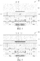
- FIG. 4 is a drawing of partial enlargement of a section view of a semiconductor device according to an embodiment of the invention. In an embodiment of the invention, FIG. 4 shows the enlargement of the semiconductor segment 40 in FIG. 3 .
- the semiconductor device 400 which may be a possible implementation of the semiconductor segment 40 as shown in FIG. 3 , may comprise a semiconductor die portion 41 and a package substrate portion 43.
- the semiconductor die portion 41 may comprise at least one silicon(Si) type substrate and an interconnection structure which contains a plurality of metal layers and dielectric layers.
- the semiconductor die portion 41 may be connected to package substrate portion 43 via solder balls (bumps) 42.
- An underfill encapsulant 421 may be comprised in the gap between the semiconductor die and package substrate around solder balls 42 to fill the gap.
- the semiconductor die portion 41 may comprise an electronic device, such as the inductor 46
- the package substrate portion 43 may comprise a shielding structure 47 placed beneath (or, under or directly below) the inductor 46 and is in a projection area of the inductor 46 in a vertical direction (e.g. a direction from the semiconductor die portion 41 to the package substrate portion 43), wherein the projection area may be the area of a projection formed on the aforementioned predetermined plane.
- the shielding structure 47 may be located within a range where the electronic device or the inductor 46 is projected on the aforementioned predetermined plane in a vertical direction.
- the package substrate may comprise a plurality of metal layers, such as the metal layers 44-1, 44-2, 45-1, 45-2, 48-1 and 48-2, where the metal layers 44-1 and 44-2 may be the same layer, the metal layers 45-1 and 45-2 may be the same layer and the metal layers 48-1 and 48-2 may be the same layer, and one or more dielectric insulation layers may be formed between the metal layers.
- the metal layers may be assigned a predetermined power or signal voltage, such as a ground voltage.
- a keep out zone such as the keep out zones 44, 45 and 48 may be provided beneath (or, under or directly below) the inductor 46 in the package substrate and disposed is in a projection area of the inductor 46 in the vertical direction.
- the shielding structure 47 may be disposed in a keep out zone of the second layer in the package substrate, such as the keep out zone 45 in the embodiment shown in FIG. 4 , under the inductor 46.
- the shielding structure 47 may be a patterned ground shield (PGS) with a plurality of stripes and a plurality of slots between the strips.
- PPS patterned ground shield
- connections may be disposed aside the shielding structure 47 to connect the shielding structure 47 to the metal layers 45-1 and 45-2.
- the metal layers 45-1 and 45-2 may be assigned ground voltage, and thus may be regarded as a ground plane. That is, the connections (as an example, ground connections) may be configured to connect the shielding structure 47 to the metal ground layer or the ground voltage of the same layer.
- the connections (as an example, ground connections) may be implemented by traces or metal lines.
- the line (which may be an invisible line) connecting the two connections may traverse the body of the shielding structure 47 and/or traverse the projection area of the inductor 46.
- the at least two ground connections GC1 and GC2 may be configured to connect the shielding structure 47 and the metal layers 45-1 and 45-2 (e.g. the ground planes).
- the line (which may be an invisible line) the at least two ground connections GC1 and GC2 may traverse the body of the shielding structure 47 and/or traverse the projection area of the inductor 46.
- the at least two ground connections GC1 and GC2 may be connected to different sides of the shielding structure to 47.
- the at least two ground connections GC1 and GC2 may be disposed above an aggressor device 49, and may be arranged along a direction in which a predetermined trace of the aggressor device 49 extends or arranged along a direction of a current flow of the aggressor device 49, where the predetermined trace may be configured to transmit power or signal.
- the direction in which a predetermined trace of the aggressor device 49 extends or the direction of a current flow of the aggressor device 49 may be the horizontal direction (e.g. from the metal layer 48-1 to the metal layer 48-2 or from the metal layer 48-2 to the metal layer 48-1).
- the line (which may be an invisible line) connecting the at least two ground connections GC1 and GC2 may also extend along the direction in which the predetermined trace of the aggressor device 49 extends or the direction of a current flow of the aggressor device 49.
- the in-package shielding structure 47 may be inserted or disposed between the inductor 46 (which may be a victim device) and the aggressor device 49. That is, the inductor 46 may be placed at one side of the in-package shielding structure 47 and the aggressor device 49 may be placed at an opposite side of the in-package shielding structure 47.
- the at least two ground connections GC1 and GC2 may also be disposed in a projection area of the aggressor device 49 in a vertical direction (e.g. a direction from the package substrate to the semiconductor die) and/or the line (which may be an invisible line) connecting the at least two ground connections GC1 and GC2 may traverse the projection area of the aggressor device 49.
- FIG. 5 is a drawing of partial enlargement of a section view of a semiconductor device according to an alternative embodiment of the invention.
- the semiconductor device 500 may comprise a semiconductor die portion 51 and a package substrate portion 53.
- the semiconductor die portion 51 may be connected to package substrate portion 53 via solder balls (bumps) 52 and a underfill encapsulant 521 may be comprised in the gap between the semiconductor die and package substrate around solder balls 52.
- a molding compound may be encapsulated surround the semiconductor die portion 51.
- the package substrate portion 53 may comprise metal layers 54-1, 54-2, 55-1, 55-2, 58-1 and 58-2, keep out zones 54, 55 and 58 and an in-package shielding structure 57.
- At least two ground connections GC1 and GC2 may be arranged along a direction in which a predetermined trace extends, where the predetermined trace may be a trace of an aggressor device 59 configured to transmit power or signal, or arranged along a direction of a current flow of the aggressor device 59.
- the semiconductor die may further comprise an on-die shielding structure 571 formed inside of the semiconductor die and disposed above the inductor 56 .
- the on-die shielding structure 571 as well as the in-package shielding structure 57 may be patterned ground shields (PGSs) with a plurality of stripes and a plurality of slots between the strips.
- PPSs ground shields
- the on-die shielding structure 571 may be disposed at one side of the inductor 56, and the in-package shielding structure 57 may be disposed at an opposite side of the inductor 56.
- FIG. 5 Most of the elements shown in FIG. 5 are the same as in FIG. 4 . Since like reference numerals in FIG. 5 refer to like features in FIG. 4 , details with respect to like elements in FIG. 5 will not be repeated herein.
- FIG. 6 is an exemplary layout showing the connections between the shielding structure and the package substrate according to an embodiment of the invention.
- FIG. 6 which is a perspective top view of a semiconductor device like FIG. 2
- there are two ground connections 64 configured to connect the in-package PGS 62 to the ground plane 60 of the package substrate.
- the ground plane may be one or more of the neighboring metal layers of the in-package shielding structure as shown in FIG. 4 and FIG. 5 .
- the ground connections may connect the in-package PGS (e.g. PGS 62) to the ground plane or the metal layers in the same layer.
- the ground connections may connect the in-package PGS (e.g.
- FIG. 7 is another exemplary layout showing the connections between the shielding structure and the package substrate according to an alternative embodiment of the invention.
- the embodiment in FIG. 7 shows a strong connection between the in-package PGS and the ground.
- the strong ground connections may connect the in-package PGS (e.g. PGS 62) to the ground plane or the metal layers in the same layer or different layers.
- An experimental result shows that, with the proposed in-package PGS and the exemplary strong ground connections as shown in FIG. 7 , at least 25 dB noise reduction in the coupling noise accused by the aggressor device located in package to the victim's on-chip inductor is achieved as compared to the semiconductor structure without the proposed in-package PGS.
- ground connections shown in FIG. 6 and FIG. 7 are merely two possible implementations and the number of ground connections that could be used in the proposed semiconductor device structure such as the structures shown in FIG. 1 to FIG. 5 is not limited to the numbers shown in FIG. 6 and FIG. 7 .
- the proposed semiconductor device structure with at least an in-package shielding structure or PGS and the corresponding ground connection(s) are effective for the suppression of the coupling noise and are able to solve the problem of unwanted coupling noise in the conventional art.
Landscapes
- Semiconductor Integrated Circuits (AREA)
- Shielding Devices Or Components To Electric Or Magnetic Fields (AREA)
- Physics & Mathematics (AREA)
- Health & Medical Sciences (AREA)
- Electromagnetism (AREA)
- Toxicology (AREA)
- Mechanical Treatment Of Semiconductor (AREA)
- Bipolar Transistors (AREA)
- Noodles (AREA)
- Non-Volatile Memory (AREA)
Applications Claiming Priority (2)
| Application Number | Priority Date | Filing Date | Title |
|---|---|---|---|
| US202163221047P | 2021-07-13 | 2021-07-13 | |
| US17/848,417 US20230014046A1 (en) | 2021-07-13 | 2022-06-24 | Semiconductor devices with in-package PGS for coupling noise suppression |
Publications (2)
| Publication Number | Publication Date |
|---|---|
| EP4120342A2 true EP4120342A2 (de) | 2023-01-18 |
| EP4120342A3 EP4120342A3 (de) | 2023-03-08 |
Family
ID=82403511
Family Applications (1)
| Application Number | Title | Priority Date | Filing Date |
|---|---|---|---|
| EP22183589.5A Pending EP4120342A3 (de) | 2021-07-13 | 2022-07-07 | Halbleiterbauelemente mit eingebauten pgs zur unterdrückung von kopplungsgeräuschen |
Country Status (4)
| Country | Link |
|---|---|
| US (1) | US20230014046A1 (de) |
| EP (1) | EP4120342A3 (de) |
| CN (1) | CN115621254A (de) |
| TW (1) | TWI815543B (de) |
Family Cites Families (26)
| Publication number | Priority date | Publication date | Assignee | Title |
|---|---|---|---|---|
| US6486534B1 (en) * | 2001-02-16 | 2002-11-26 | Ashvattha Semiconductor, Inc. | Integrated circuit die having an interference shield |
| US8324028B2 (en) * | 2006-12-01 | 2012-12-04 | Infineon Technologies Ag | Assembly comprising a support element and a chip, support element, method for shielding, and method for protecting |
| JP5103032B2 (ja) * | 2007-03-01 | 2012-12-19 | ルネサスエレクトロニクス株式会社 | 半導体装置 |
| US7911014B2 (en) * | 2007-09-29 | 2011-03-22 | My The Doan | On chip antenna and method of manufacturing the same |
| US7884390B2 (en) * | 2007-10-02 | 2011-02-08 | Fairchild Semiconductor Corporation | Structure and method of forming a topside contact to a backside terminal of a semiconductor device |
| US8492872B2 (en) * | 2007-10-05 | 2013-07-23 | Taiwan Semiconductor Manufacturing Co., Ltd. | On-chip inductors with through-silicon-via fence for Q improvement |
| US8013258B2 (en) * | 2008-06-11 | 2011-09-06 | Mediatek Inc. | Shielding device |
| JP5216532B2 (ja) * | 2008-10-30 | 2013-06-19 | 株式会社日立製作所 | 半導体集積回路 |
| US8143097B2 (en) * | 2009-09-23 | 2012-03-27 | Stats Chippac, Ltd. | Semiconductor device and method of forming open cavity in TSV interposer to contain semiconductor die in WLCSMP |
| JP5551480B2 (ja) * | 2010-03-24 | 2014-07-16 | ルネサスエレクトロニクス株式会社 | 半導体装置および半導体装置の製造方法 |
| US8659126B2 (en) * | 2011-12-07 | 2014-02-25 | Taiwan Semiconductor Manufacturing Company, Ltd. | Integrated circuit ground shielding structure |
| US20130134553A1 (en) * | 2011-11-30 | 2013-05-30 | Taiwan Semiconductor Manufacturing Co., Ltd. | Interposer and semiconductor package with noise suppression features |
| TWI509771B (zh) * | 2013-03-25 | 2015-11-21 | 瑞昱半導體股份有限公司 | 積體電感結構以及積體電感結構製造方法 |
| KR102214798B1 (ko) * | 2014-02-05 | 2021-02-10 | 삼성전자주식회사 | 패키지 기판 및 이를 포함하는 반도체 패키지 |
| US20160211221A1 (en) * | 2015-01-16 | 2016-07-21 | Amkor Technology, Inc. | Semiconductor device and manufacturing method thereof |
| US20170040266A1 (en) * | 2015-05-05 | 2017-02-09 | Mediatek Inc. | Fan-out package structure including antenna |
| US9691720B2 (en) * | 2015-07-27 | 2017-06-27 | Qualcomm Incorporated | Multi-layer ground shield structure of interconnected elements |
| US10068856B2 (en) * | 2016-07-12 | 2018-09-04 | Mediatek Inc. | Integrated circuit apparatus |
| TWI645428B (zh) * | 2016-11-25 | 2018-12-21 | 瑞昱半導體股份有限公司 | 積體電感 |
| JP7407498B2 (ja) * | 2017-09-15 | 2024-01-04 | 日東電工株式会社 | 配線回路基板およびその製造方法 |
| CN110610924B (zh) * | 2018-06-15 | 2021-04-20 | 中芯国际集成电路制造(上海)有限公司 | 半导体器件及其形成方法、半导体结构 |
| US11588009B2 (en) * | 2018-12-12 | 2023-02-21 | Amkor Technology Singapore Holding Pte. Ltd. | Semiconductor device having a lid configured as an enclosure and a capacitive structure and method of manufacturing a semiconductor device |
| US10644479B1 (en) * | 2019-02-23 | 2020-05-05 | Amkor Technology Singapore Holding Pte Ltd. | Semiconductor device and method of manufacturing a semiconductor device |
| US20230253390A1 (en) * | 2022-02-07 | 2023-08-10 | Mediatek Inc. | Semiconductor package assembly |
| US20240038690A1 (en) * | 2022-07-26 | 2024-02-01 | Mediatek Inc. | Semiconductor devices with a structure capable of suppressing coupling noise suppression |
| US20240355728A1 (en) * | 2023-04-21 | 2024-10-24 | Taiwan Semiconductor Manufacturing Company, Ltd. | Semiconductor structure |
-
2022
- 2022-06-24 US US17/848,417 patent/US20230014046A1/en active Pending
- 2022-06-30 CN CN202210772548.2A patent/CN115621254A/zh active Pending
- 2022-07-07 TW TW111125520A patent/TWI815543B/zh active
- 2022-07-07 EP EP22183589.5A patent/EP4120342A3/de active Pending
Also Published As
| Publication number | Publication date |
|---|---|
| EP4120342A3 (de) | 2023-03-08 |
| US20230014046A1 (en) | 2023-01-19 |
| CN115621254A (zh) | 2023-01-17 |
| TWI815543B (zh) | 2023-09-11 |
| TW202303908A (zh) | 2023-01-16 |
Similar Documents
| Publication | Publication Date | Title |
|---|---|---|
| US20250096151A1 (en) | Wire bonding method and apparatus for electromagnetic interference shielding | |
| KR102246040B1 (ko) | 회로 모듈 | |
| CN103137602B (zh) | 带有抑噪部件的中介层以及半导体封装件 | |
| US7088009B2 (en) | Wirebonded assemblage method and apparatus | |
| US7795709B2 (en) | Shielding noisy conductors in integrated passive devices | |
| KR102620863B1 (ko) | 전자기간섭 차폐층을 갖는 반도체 패키지 및 그 제조방법 | |
| KR19990037427A (ko) | 저인덕턴스 집적 회로 패키지 | |
| KR20250044114A (ko) | 전자기 차폐 구조 및 패키징 방법 | |
| WO2014012370A1 (zh) | 一种芯片封装及封装方法 | |
| KR102279978B1 (ko) | 모듈 | |
| US20120248585A1 (en) | Electromagnetic interference shielding structure for integrated circuit substrate and method for fabricating the same | |
| US10923434B2 (en) | Semiconductor packages having EMI shielding layers | |
| KR102279979B1 (ko) | 모듈 | |
| CN210489609U (zh) | 集成电路封装体 | |
| CN220233160U (zh) | 电路模块 | |
| KR100895816B1 (ko) | 반도체 패키지 | |
| US20230014046A1 (en) | Semiconductor devices with in-package PGS for coupling noise suppression | |
| JP2022165445A (ja) | 半導体装置 | |
| US9609742B2 (en) | Electrical characteristics of package substrates and semiconductor packages including the same | |
| JPH0864983A (ja) | シールドケース | |
| EP3125282B1 (de) | Oberflächenmontierte hochfrequenzschaltung | |
| JPH1140709A (ja) | 半導体実装構造およびその製造方法 | |
| KR102886839B1 (ko) | 통신 모듈 | |
| KR101305581B1 (ko) | 차폐 부재 및 이를 포함하는 인쇄회로기판 | |
| US7361981B2 (en) | Pad layout |
Legal Events
| Date | Code | Title | Description |
|---|---|---|---|
| PUAI | Public reference made under article 153(3) epc to a published international application that has entered the european phase |
Free format text: ORIGINAL CODE: 0009012 |
|
| STAA | Information on the status of an ep patent application or granted ep patent |
Free format text: STATUS: THE APPLICATION HAS BEEN PUBLISHED |
|
| AK | Designated contracting states |
Kind code of ref document: A2 Designated state(s): AL AT BE BG CH CY CZ DE DK EE ES FI FR GB GR HR HU IE IS IT LI LT LU LV MC MK MT NL NO PL PT RO RS SE SI SK SM TR |
|
| PUAL | Search report despatched |
Free format text: ORIGINAL CODE: 0009013 |
|
| AK | Designated contracting states |
Kind code of ref document: A3 Designated state(s): AL AT BE BG CH CY CZ DE DK EE ES FI FR GB GR HR HU IE IS IT LI LT LU LV MC MK MT NL NO PL PT RO RS SE SI SK SM TR |
|
| RIC1 | Information provided on ipc code assigned before grant |
Ipc: H01L 23/498 20060101ALI20230201BHEP Ipc: H01L 23/522 20060101ALI20230201BHEP Ipc: H01L 23/552 20060101AFI20230201BHEP |
|
| P01 | Opt-out of the competence of the unified patent court (upc) registered |
Effective date: 20230607 |
|
| STAA | Information on the status of an ep patent application or granted ep patent |
Free format text: STATUS: REQUEST FOR EXAMINATION WAS MADE |
|
| 17P | Request for examination filed |
Effective date: 20230907 |
|
| RBV | Designated contracting states (corrected) |
Designated state(s): AL AT BE BG CH CY CZ DE DK EE ES FI FR GB GR HR HU IE IS IT LI LT LU LV MC MK MT NL NO PL PT RO RS SE SI SK SM TR |