EP4099685B1 - Bildgebendes element, bildgebende vorrichtung und abstandsmessvorrichtung - Google Patents
Bildgebendes element, bildgebende vorrichtung und abstandsmessvorrichtung Download PDFInfo
- Publication number
- EP4099685B1 EP4099685B1 EP21747394.1A EP21747394A EP4099685B1 EP 4099685 B1 EP4099685 B1 EP 4099685B1 EP 21747394 A EP21747394 A EP 21747394A EP 4099685 B1 EP4099685 B1 EP 4099685B1
- Authority
- EP
- European Patent Office
- Prior art keywords
- unit
- pixel
- light
- signal
- imaging
- Prior art date
- Legal status (The legal status is an assumption and is not a legal conclusion. Google has not performed a legal analysis and makes no representation as to the accuracy of the status listed.)
- Active
Links
Images




















Classifications
-
- H—ELECTRICITY
- H04—ELECTRIC COMMUNICATION TECHNIQUE
- H04N—PICTORIAL COMMUNICATION, e.g. TELEVISION
- H04N25/00—Circuitry of solid-state image sensors [SSIS]; Control thereof
- H04N25/70—SSIS architectures; Circuits associated therewith
- H04N25/76—Addressed sensors, e.g. MOS or CMOS sensors
- H04N25/766—Addressed sensors, e.g. MOS or CMOS sensors comprising control or output lines used for a plurality of functions, e.g. for pixel output, driving, reset or power
-
- G—PHYSICS
- G01—MEASURING; TESTING
- G01S—RADIO DIRECTION-FINDING; RADIO NAVIGATION; DETERMINING DISTANCE OR VELOCITY BY USE OF RADIO WAVES; LOCATING OR PRESENCE-DETECTING BY USE OF THE REFLECTION OR RERADIATION OF RADIO WAVES; ANALOGOUS ARRANGEMENTS USING OTHER WAVES
- G01S17/00—Systems using the reflection or reradiation of electromagnetic waves other than radio waves, e.g. lidar systems
- G01S17/88—Lidar systems specially adapted for specific applications
- G01S17/89—Lidar systems specially adapted for specific applications for mapping or imaging
- G01S17/894—Three-dimensional [3D] imaging with simultaneous measurement of time-of-flight at a two-dimensional [2D] array of receiver pixels, e.g. time-of-flight cameras or flash lidar
-
- G—PHYSICS
- G01—MEASURING; TESTING
- G01S—RADIO DIRECTION-FINDING; RADIO NAVIGATION; DETERMINING DISTANCE OR VELOCITY BY USE OF RADIO WAVES; LOCATING OR PRESENCE-DETECTING BY USE OF THE REFLECTION OR RERADIATION OF RADIO WAVES; ANALOGOUS ARRANGEMENTS USING OTHER WAVES
- G01S7/00—Details of systems according to groups G01S13/00, G01S15/00, G01S17/00
- G01S7/48—Details of systems according to groups G01S13/00, G01S15/00, G01S17/00 of systems according to group G01S17/00
- G01S7/481—Constructional features, e.g. arrangements of optical elements
- G01S7/4816—Constructional features, e.g. arrangements of optical elements of receivers alone
-
- G—PHYSICS
- G01—MEASURING; TESTING
- G01S—RADIO DIRECTION-FINDING; RADIO NAVIGATION; DETERMINING DISTANCE OR VELOCITY BY USE OF RADIO WAVES; LOCATING OR PRESENCE-DETECTING BY USE OF THE REFLECTION OR RERADIATION OF RADIO WAVES; ANALOGOUS ARRANGEMENTS USING OTHER WAVES
- G01S7/00—Details of systems according to groups G01S13/00, G01S15/00, G01S17/00
- G01S7/48—Details of systems according to groups G01S13/00, G01S15/00, G01S17/00 of systems according to group G01S17/00
- G01S7/483—Details of pulse systems
- G01S7/486—Receivers
-
- G—PHYSICS
- G01—MEASURING; TESTING
- G01S—RADIO DIRECTION-FINDING; RADIO NAVIGATION; DETERMINING DISTANCE OR VELOCITY BY USE OF RADIO WAVES; LOCATING OR PRESENCE-DETECTING BY USE OF THE REFLECTION OR RERADIATION OF RADIO WAVES; ANALOGOUS ARRANGEMENTS USING OTHER WAVES
- G01S7/00—Details of systems according to groups G01S13/00, G01S15/00, G01S17/00
- G01S7/48—Details of systems according to groups G01S13/00, G01S15/00, G01S17/00 of systems according to group G01S17/00
- G01S7/491—Details of non-pulse systems
- G01S7/4912—Receivers
- G01S7/4913—Circuits for detection, sampling, integration or read-out
- G01S7/4914—Circuits for detection, sampling, integration or read-out of detector arrays, e.g. charge-transfer gates
-
- G—PHYSICS
- G01—MEASURING; TESTING
- G01S—RADIO DIRECTION-FINDING; RADIO NAVIGATION; DETERMINING DISTANCE OR VELOCITY BY USE OF RADIO WAVES; LOCATING OR PRESENCE-DETECTING BY USE OF THE REFLECTION OR RERADIATION OF RADIO WAVES; ANALOGOUS ARRANGEMENTS USING OTHER WAVES
- G01S7/00—Details of systems according to groups G01S13/00, G01S15/00, G01S17/00
- G01S7/48—Details of systems according to groups G01S13/00, G01S15/00, G01S17/00 of systems according to group G01S17/00
- G01S7/491—Details of non-pulse systems
- G01S7/4912—Receivers
- G01S7/4915—Time delay measurement, e.g. operational details for pixel components; Phase measurement
-
- H—ELECTRICITY
- H04—ELECTRIC COMMUNICATION TECHNIQUE
- H04N—PICTORIAL COMMUNICATION, e.g. TELEVISION
- H04N25/00—Circuitry of solid-state image sensors [SSIS]; Control thereof
- H04N25/50—Control of the SSIS exposure
- H04N25/57—Control of the dynamic range
- H04N25/59—Control of the dynamic range by controlling the amount of charge storable in the pixel, e.g. modification of the charge conversion ratio of the floating node capacitance
-
- H—ELECTRICITY
- H04—ELECTRIC COMMUNICATION TECHNIQUE
- H04N—PICTORIAL COMMUNICATION, e.g. TELEVISION
- H04N25/00—Circuitry of solid-state image sensors [SSIS]; Control thereof
- H04N25/60—Noise processing, e.g. detecting, correcting, reducing or removing noise
- H04N25/65—Noise processing, e.g. detecting, correcting, reducing or removing noise applied to reset noise, e.g. KTC noise related to CMOS structures by techniques other than CDS
-
- H—ELECTRICITY
- H04—ELECTRIC COMMUNICATION TECHNIQUE
- H04N—PICTORIAL COMMUNICATION, e.g. TELEVISION
- H04N25/00—Circuitry of solid-state image sensors [SSIS]; Control thereof
- H04N25/70—SSIS architectures; Circuits associated therewith
- H04N25/703—SSIS architectures incorporating pixels for producing signals other than image signals
- H04N25/705—Pixels for depth measurement, e.g. RGBZ
-
- H—ELECTRICITY
- H04—ELECTRIC COMMUNICATION TECHNIQUE
- H04N—PICTORIAL COMMUNICATION, e.g. TELEVISION
- H04N25/00—Circuitry of solid-state image sensors [SSIS]; Control thereof
- H04N25/70—SSIS architectures; Circuits associated therewith
- H04N25/71—Charge-coupled device [CCD] sensors; Charge-transfer registers specially adapted for CCD sensors
-
- H—ELECTRICITY
- H04—ELECTRIC COMMUNICATION TECHNIQUE
- H04N—PICTORIAL COMMUNICATION, e.g. TELEVISION
- H04N25/00—Circuitry of solid-state image sensors [SSIS]; Control thereof
- H04N25/70—SSIS architectures; Circuits associated therewith
- H04N25/76—Addressed sensors, e.g. MOS or CMOS sensors
- H04N25/77—Pixel circuitry, e.g. memories, A/D converters, pixel amplifiers, shared circuits or shared components
-
- H—ELECTRICITY
- H04—ELECTRIC COMMUNICATION TECHNIQUE
- H04N—PICTORIAL COMMUNICATION, e.g. TELEVISION
- H04N25/00—Circuitry of solid-state image sensors [SSIS]; Control thereof
- H04N25/70—SSIS architectures; Circuits associated therewith
- H04N25/76—Addressed sensors, e.g. MOS or CMOS sensors
- H04N25/77—Pixel circuitry, e.g. memories, A/D converters, pixel amplifiers, shared circuits or shared components
- H04N25/771—Pixel circuitry, e.g. memories, A/D converters, pixel amplifiers, shared circuits or shared components comprising storage means other than floating diffusion
-
- H—ELECTRICITY
- H04—ELECTRIC COMMUNICATION TECHNIQUE
- H04N—PICTORIAL COMMUNICATION, e.g. TELEVISION
- H04N25/00—Circuitry of solid-state image sensors [SSIS]; Control thereof
- H04N25/70—SSIS architectures; Circuits associated therewith
- H04N25/76—Addressed sensors, e.g. MOS or CMOS sensors
- H04N25/77—Pixel circuitry, e.g. memories, A/D converters, pixel amplifiers, shared circuits or shared components
- H04N25/772—Pixel circuitry, e.g. memories, A/D converters, pixel amplifiers, shared circuits or shared components comprising A/D, V/T, V/F, I/T or I/F converters
-
- H—ELECTRICITY
- H04—ELECTRIC COMMUNICATION TECHNIQUE
- H04N—PICTORIAL COMMUNICATION, e.g. TELEVISION
- H04N25/00—Circuitry of solid-state image sensors [SSIS]; Control thereof
- H04N25/70—SSIS architectures; Circuits associated therewith
- H04N25/79—Arrangements of circuitry being divided between different or multiple substrates, chips or circuit boards, e.g. stacked image sensors
-
- H—ELECTRICITY
- H10—SEMICONDUCTOR DEVICES; ELECTRIC SOLID-STATE DEVICES NOT OTHERWISE PROVIDED FOR
- H10F—INORGANIC SEMICONDUCTOR DEVICES SENSITIVE TO INFRARED RADIATION, LIGHT, ELECTROMAGNETIC RADIATION OF SHORTER WAVELENGTH OR CORPUSCULAR RADIATION
- H10F39/00—Integrated devices, or assemblies of multiple devices, comprising at least one element covered by group H10F30/00, e.g. radiation detectors comprising photodiode arrays
- H10F39/10—Integrated devices
- H10F39/12—Image sensors
- H10F39/18—Complementary metal-oxide-semiconductor [CMOS] image sensors; Photodiode array image sensors
-
- H—ELECTRICITY
- H10—SEMICONDUCTOR DEVICES; ELECTRIC SOLID-STATE DEVICES NOT OTHERWISE PROVIDED FOR
- H10F—INORGANIC SEMICONDUCTOR DEVICES SENSITIVE TO INFRARED RADIATION, LIGHT, ELECTROMAGNETIC RADIATION OF SHORTER WAVELENGTH OR CORPUSCULAR RADIATION
- H10F39/00—Integrated devices, or assemblies of multiple devices, comprising at least one element covered by group H10F30/00, e.g. radiation detectors comprising photodiode arrays
- H10F39/10—Integrated devices
- H10F39/12—Image sensors
- H10F39/18—Complementary metal-oxide-semiconductor [CMOS] image sensors; Photodiode array image sensors
- H10F39/186—Complementary metal-oxide-semiconductor [CMOS] image sensors; Photodiode array image sensors having arrangements for blooming suppression
- H10F39/1865—Overflow drain structures
-
- H—ELECTRICITY
- H10—SEMICONDUCTOR DEVICES; ELECTRIC SOLID-STATE DEVICES NOT OTHERWISE PROVIDED FOR
- H10F—INORGANIC SEMICONDUCTOR DEVICES SENSITIVE TO INFRARED RADIATION, LIGHT, ELECTROMAGNETIC RADIATION OF SHORTER WAVELENGTH OR CORPUSCULAR RADIATION
- H10F39/00—Integrated devices, or assemblies of multiple devices, comprising at least one element covered by group H10F30/00, e.g. radiation detectors comprising photodiode arrays
- H10F39/80—Constructional details of image sensors
- H10F39/802—Geometry or disposition of elements in pixels, e.g. address-lines or gate electrodes
-
- H—ELECTRICITY
- H10—SEMICONDUCTOR DEVICES; ELECTRIC SOLID-STATE DEVICES NOT OTHERWISE PROVIDED FOR
- H10F—INORGANIC SEMICONDUCTOR DEVICES SENSITIVE TO INFRARED RADIATION, LIGHT, ELECTROMAGNETIC RADIATION OF SHORTER WAVELENGTH OR CORPUSCULAR RADIATION
- H10F39/00—Integrated devices, or assemblies of multiple devices, comprising at least one element covered by group H10F30/00, e.g. radiation detectors comprising photodiode arrays
- H10F39/80—Constructional details of image sensors
- H10F39/803—Pixels having integrated switching, control, storage or amplification elements
- H10F39/8033—Photosensitive area
-
- H—ELECTRICITY
- H10—SEMICONDUCTOR DEVICES; ELECTRIC SOLID-STATE DEVICES NOT OTHERWISE PROVIDED FOR
- H10F—INORGANIC SEMICONDUCTOR DEVICES SENSITIVE TO INFRARED RADIATION, LIGHT, ELECTROMAGNETIC RADIATION OF SHORTER WAVELENGTH OR CORPUSCULAR RADIATION
- H10F39/00—Integrated devices, or assemblies of multiple devices, comprising at least one element covered by group H10F30/00, e.g. radiation detectors comprising photodiode arrays
- H10F39/80—Constructional details of image sensors
- H10F39/803—Pixels having integrated switching, control, storage or amplification elements
- H10F39/8037—Pixels having integrated switching, control, storage or amplification elements the integrated elements comprising a transistor
-
- H—ELECTRICITY
- H10—SEMICONDUCTOR DEVICES; ELECTRIC SOLID-STATE DEVICES NOT OTHERWISE PROVIDED FOR
- H10F—INORGANIC SEMICONDUCTOR DEVICES SENSITIVE TO INFRARED RADIATION, LIGHT, ELECTROMAGNETIC RADIATION OF SHORTER WAVELENGTH OR CORPUSCULAR RADIATION
- H10F39/00—Integrated devices, or assemblies of multiple devices, comprising at least one element covered by group H10F30/00, e.g. radiation detectors comprising photodiode arrays
- H10F39/80—Constructional details of image sensors
- H10F39/811—Interconnections
-
- H—ELECTRICITY
- H04—ELECTRIC COMMUNICATION TECHNIQUE
- H04N—PICTORIAL COMMUNICATION, e.g. TELEVISION
- H04N25/00—Circuitry of solid-state image sensors [SSIS]; Control thereof
- H04N25/60—Noise processing, e.g. detecting, correcting, reducing or removing noise
Definitions
- the present technology relates to an imaging element, an imaging device, and a ranging device and to, for example, an imaging element, an imaging device, and a ranging device capable of reducing noise.
- imaging elements such as charge coupled device (CCD) or complementary metal oxide semiconductor (CMOS) image sensors are used in electronic devices that have imaging functions of digital still cameras or digital video cameras.
- CCD charge coupled device
- CMOS complementary metal oxide semiconductor
- Each imaging element includes pixels in which a photodiode (PD) performing photoelectric conversion and a plurality of transistors are embedded, and an image is constructed based on pixel signals output from the plurality of pixels arrayed in a planar form.
- the pixel signals output from the pixels are subjected to analog to digital (AD) conversion in parallel and output by, for example, a plurality of AD converters disposed in every column of the pixels.
- AD analog to digital
- PTL 1 proposes that reading is performed twice before and after exposure start as a scheme of performing cancelation including kTC noise of each pixel.
- resetting is applied before the exposure start, a reset signal of each pixel is acquired for all the effective pixels, and the reset signal is stored as digital data in a memory or the like.
- CDS is performed with the digital data which is subtracted from accumulated signals acquired after exposure is completed.
- WO 2017/154605 A1 is related to an imaging device and electronic equipment that make it possible to enlarge the dynamic range of the imaging device without degrading the image quality.
- a first photoelectric converter for which the amount of charge converted per unit of time is smaller than that of the first photoelectric converter; a charge storage part for storing the charge generated by the second photoelectric converter; a charge-voltage converter; a first transfer gate part for transferring the charge from the first photoelectric converter to the charge-voltage converter; a second transfer gate part for combining the potential of the charge-voltage converter and the charge storage part; a third transfer gate part for transferring the charge from the second photoelectric converter to the charge storage part; an overflow path, formed on the bottom of the gate electrode of the third transfer gate part, for transferring charge that overflowed from the second photoelectric converter to the charge storage part; and a light reducing part for reducing light that impinges on the second photoelectric converter.
- EP 3 598 167 A1 is concerned with a light-receiving element which includes an on-chip lens; an interconnection layer; and a semiconductor layer that is disposed between the on-chip lens and the interconnection layer.
- the semiconductor layer includes a first voltage application unit to which a first voltage is applied, a second voltage application unit to which a second voltage different from the first voltage is applied, a first charge detection unit that is disposed at the periphery of the first voltage application unit, a second charge detection unit that is disposed at the periphery of the second voltage application unit, and a charge discharge region that is provided on an outer side of an effective pixel region.
- the present technology is applicable to a light-receiving element that generates distance information in a ToF method.
- EP 3 598 499 A2 discloses a light receiving element including an on-chip lens, a wiring layer, and a semiconductor layer disposed between the on-chip lens and the wiring layer.
- the semiconductor layer includes a photodiode, a first transfer transistor that transfers electric charge generated in the photodiode to a first charge storage portion, a second transfer transistor that transfers electric charge generated in the photodiode to a second charge storage portion, and an interpixel separation portion that separates the semiconductor layers of adjacent pixels from each other, for at least part of the semiconductor layer in the depth direction.
- the wiring layer has at least one layer including a light blocking member. The light blocking member is disposed to overlap with the photodiode in a plan view.
- WO 2018/221261 A1 relates to a solid-state imaging device and an electronic device capable of effectively preventing blooming.
- a solid-state imaging device including: a pixel array portion in which a plurality of pixels is two-dimensionally arranged, in which the pixels each include an in-pixel capacitance and a counter electrode of the in-pixel capacitance, the in-pixel capacitance being provided on a side opposite to a light incident surface of a photoelectric conversion element provided in a semiconductor substrate, the counter electrode being provided in the semiconductor substrate.
- the present disclosure can be applied to a back-illuminated CMOS image sensor.
- the present technology has been devised in such circumstances and is capable of reducing noise.
- Fig. 1 is a block diagram illustrating an exemplary functional configuration of an imaging device 10 according to an embodiment of the present technology.
- the imaging device 10 is, for example, a rear surface irradiation type image sensor of a so-called global shutter scheme, such as a complementary metal oxide semiconductor (CMOS) image sensor.
- CMOS complementary metal oxide semiconductor
- the global shutter scheme is a scheme of basically performing global exposure by starting exposure of all the pixels simultaneously and ending the exposure of all the pixels simultaneously.
- all the pixels are all the pixels of a portion appearing in an image and dummy pixels or the like are excluded.
- a scheme of moving a region subjected to global exposure while performing the global exposure in units of a plurality of rows (for example, tens of rows) rather than simultaneously in all the pixels is also included in the global shutter scheme.
- a scheme of performing global exposure on pixels of a predetermined region rather than all the pixels of a portion appearing in an image is also included in the global shutter scheme.
- a rear surface irradiation type image sensor is an image sensor configured such that a photoelectric conversion unit such as a photodiode that receives light from a subject and converts the light into an electrical signal is provided between a light reception surface on which the light is incident from the subject and a wiring layer in which a wiring such as a transistor driving each pixel is provided.
- a photoelectric conversion unit such as a photodiode that receives light from a subject and converts the light into an electrical signal is provided between a light reception surface on which the light is incident from the subject and a wiring layer in which a wiring such as a transistor driving each pixel is provided.
- the imaging device 10 includes, for example, a pixel array unit 21, a vertical driving unit 22, a column signal processing unit 23, a data storage unit 29, a horizontal driving unit 24, a system control unit 25, and a signal processing unit 28.
- the pixel array unit 21 is formed on a semiconductor substrate 11 (to be described below). Peripheral circuits such as the vertical driving unit 22, the column signal processing unit 23, the data storage unit 29, the horizontal driving unit 24, the system control unit 25, and the signal processing unit 28 are formed on, for example, the same semiconductor substrate 11 as the pixel array unit 21.
- the pixel array unit 21 includes a plurality of pixels 20 including photoelectric conversion units (to be described below) that generate and accumulate charges in accordance with an amount of light incident from the subject.
- the pixels 20 are arrayed in the horizontal direction (the row direction) and the vertical direction (the column direction), as illustrated in Fig. 1 .
- a pixel driving line 26 is wired in the row direction for each pixel row formed by the pixels 20 arrayed in a line in the row direction
- a vertical signal line (VSL) 28 is wired in the column direction for each pixel column formed by the pixels 20 arrayed in a line in the column direction.
- VSL vertical signal line
- the vertical driving unit 22 is configured with a shift register or an address decoder.
- the vertical driving unit 22 simultaneously drives all the plurality of pixels 20 in the pixel array unit 21 or drives the pixels 20 in units of pixel rows by supplying signals or the like to the plurality of pixels 20 through the plurality of pixel driving lines 26.
- the vertical driving unit 22 includes, for example, two scanning systems, a reading scanning system and a sweeping scanning system.
- the reading scanning system selectively scans unit pixels of the pixel array unit 21 in sequence to read signals from the unit pixels in units of rows.
- the sweeping scanning system performs sweeping scanning on read rows in which the reading scanning is performed by the readings scanning system earlier than the reading scanning by a time of a shutter speed.
- a so-called electronic shutter operation is performed by casing the sweeping scanning system to sweep unnecessary charges, that is, resetting.
- the electronic shutter operation is an operation of discarding photoelectric charges of the photoelectric conversion unit 51 and newly starting exposure, that is, newly starting accumulation of the photoelectric charges.
- a signal read through a reading operation by the reading scanning system corresponds to an amount of light incident after an immediately previous reading operation or an electronic shutter operation.
- a period from a reading timing of the immediately previous reading operation or a sweeping timing of the electronic shutter operation to a reading timing of a present reading operation is an accumulation time of photoelectric charges in the unit pixels, that is, an exposure time.
- a signal output from each unit pixel of a pixel row selectively scanned by the vertical driving unit 22 is supplied to the column signal processing unit 23 through each vertical signal line 27.
- the column signal processing unit 23 performs predetermined signal processing on the signal output through a VSL 27 from each unit pixel of the selected row for each pixel column of the pixel array unit 21 and temporarily retains a pixel signal subjected to the signal processing.
- the column signal processing unit 23 is configured with, for example, a shift register or an address decoder and generates a digital pixel signal by performing noise removal processing, correlated double sampling processing, analog/digital (A/D) conversion A/D conversion processing on an analog pixel signal, and the like.
- the column signal processing unit 23 supplies the generated pixel signal to the signal processing unit 28.
- the horizontal driving unit 24 is configured with a shift register, an address decoder or the like and selects the unit circuits corresponding to a pixel column of the column signal processing unit 23 in sequence. Through the selective scanning of the horizontal driving unit 24, the pixel signals subjected to the signal processing on each unit circuit in the column signal processing unit 23 are output in sequence to the signal processing unit 28.
- the system control unit 25 is configured with a timing generator or the like that generates various timing signals.
- the system control unit 25 performs driving control on the vertical driving unit 22, the column signal processing unit 23, and the horizontal driving unit 24 based on a timing signal generated by the timing generator.
- the signal processing unit 28 performs signal processing such as arithmetic processing on the pixel signal supplied from the column signal processing unit 23 while temporarily storing data in the data storage unit 29 as necessary, and outputs an image signal formed from each pixel signal.
- the data storage unit 29 temporarily store data necessary for the signal processing during the signal processing of the signal processing unit 28.
- Fig. 2 is a diagram illustrating an exemplary circuit configuration of any one pixel 20 among the plurality of pixels 20 provided in the pixel array unit 21.
- the pixel 20 illustrated in Fig. 2 is referred to as the pixel 20 in the first embodiment and is referred to as a pixel 20a for distinguishment from pixels of other embodiments.
- the pixel 20a implements an FD type global shutter.
- the pixel 20a in the pixel array unit 21 includes, for example, a photoelectric conversion unit (PD) 51, a charge transfer unit (TG) 52, a floating diffusion (FD) 53 serving as a charge retention unit and a charge voltage conversion unit, a reset transistor (RST) 54, a feedback enable transistor (FBEN) 55, a discharge transistor (OFG) 56, an amplification transistor (AMP) 57, a select transistor (SEL) 58, a conversion efficiency switching transistor (FDG) 59, and an additional capacitance unit 60.
- PD photoelectric conversion unit
- TG charge transfer unit
- FD floating diffusion
- RST reset transistor
- FBEN feedback enable transistor
- OFG discharge transistor
- AMP amplification transistor
- SEL select transistor
- FDG conversion efficiency switching transistor
- the TG 52, the FD 53, the RST 54, the FBEN 55, the OFG 56, the AMP 57, and the SEL 58 are all N-type MOS transistors.
- a gate electrode of each of the TG 52, the FD 53, the RST 54, the FBEN 55, the OFG 56, the AMP 57, and the SEL 58 is supplied with a driving signal.
- Each driving signal is a pulse signal in which a high level state is an active state, that is, an ON state and a low level state is an inactive state, that is, an OFF state.
- setting a driving signal to the active state is also referred to turning a driving signal on and setting a driving signal to the inactive state is also referred to as turning the driving signal off.
- CFD is a capacitance value of the FD 53 and CFD2 is a capacitance value of the additional capacitance unit 60
- the capacitance value C in a region of the pixel in which reading of a signal level is performed is CFD+CFD2 in the state in which the driving signal FDG is turned on.
- the driving signal FDG is turned off
- the capacitance value C is changed to CFD. Therefore, sensitivity (a change amount of a voltage: FD conversion efficiency) of a voltage with respect to the change amount of the charges is raised.
- sensitivity of the pixel is appropriately changed by turning the driving signal FDG on or off.
- the driving signal FDG is turned on, the additional capacitance unit 60 is electrically connected to the FD 53. Therefore, some of the charges transferred from the PD 61 to the FD 53 are accumulated not only in the FD 53 but also in the additional capacitance unit 60.
- the RST 54 includes a drain connected to the FBEN 55 and a source connected to the FD 53.
- the RST 54 functions as a reset unit that initializes, that is, resets, the FD 53 in accordance with a driving signal applied to the gate electrode.
- the drain of the RST 54 forms a parasitic capacitance C_ST with the grounding and a parasitic capacitance C_FB with the gate electrode of the AMP 57.
- the SEL 58 is connected between the source of the AMP 57 and the VSL 28 to supply a select signal to the gate electrode of the SEL 58.
- the select signal When the select signal is turned on, the SEL 58 enters a conductive state and the pixel 20a where the SEL 58 is provided enters a selection state.
- the pixel 20a When the pixel 20a enters the selection state, a pixel signal output from the AMP 57 is read through the VSL 28 by the column signal processing unit 23.
- the plurality of pixel driving lines 26 are each wired, for example, for each pixel row.
- Each driving signal is supplied from the vertical driving unit 22 to the selected pixel 20a through the plurality of pixel driving lines 26.
- the pixel circuit illustrated in Fig. 2 is an example of a pixel circuit which can be used in the pixel array unit 21 and a pixel circuit that has a different configuration can also be used.
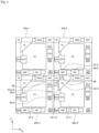
- Fig. 3 is a plan view illustrating a configuration of the pixel 20a according to the first embodiment.
- the left and right directions in the drawings are referred to as the X axis direction and the upward and downward directions in the drawings are referred to as the Y axis direction.
- the X direction corresponds to the row direction (the horizontal direction) of Fig. 2 and the Y direction corresponds to the column direction (the vertical direction) of Fig. 2 in the following description.
- the PD 51 is provided in a region of a central portion of the rectangular pixel 20a.
- the TG 52 is provided on the top left side of the PD 51 in the drawing.
- the TG 52 is a gate portion of the transfer transistor 52.
- An FD53-1 is provided on the top side of the TG 52,
- the FD 53 is formed from two regions of an FD 53-1 and an FD53-2.
- the FD 53-1 and the FD 53-2 are connected in a wiring layer (not illustrated) of a lower layer and are configured to function as one FD 53.
- the FD 53-1 and the FD 53-2 formed inside the same pixel 20a can also be connected.
- the FD 53-1 and the FD 53-2 formed in another pixel 20a can also be connected.
- the two regions of the FD 53-1 and the FD 53-2 are regions formed in a substrate (for example, a silicon substrate) in which the PD 51 is formed.
- a region is assumed to be a region in the substrate in which the PD 51 is formed unless particularly mentioned.
- the FD 53 is configured from the FD 53-1 and the FD 53-2 formed in different regions in the substrate.
- the FD 53 is formed by connecting a plurality of regions distributed and formed in the substrate by wirings.
- the different regions are assumed to be a plurality of regions in the substrate or regions distributed and formed in the substrate.
- the FD 53-2 is formed at a position coming into contact with the FDG 59.
- the FDG 59 is provided on the right side of the PD 51 in the drawing and the FD 53-2 is formed on the upper side of the FDG 59.
- the additional capacitance unit (FDext) 60 is formed on the lower side of the FDG 59 in the drawing. Since the FD 53 is formed in two regions of the FD 53-1 and FD 53-2, the capacitance of the FD 53 itself can be increased. By providing the FDG 59 and the additional capacitance unit 60, the capacitance of the FD 53 can be further increased.
- the RST 54 is formed on the top right side of the PD 51 in the drawing.
- the FBEN 55 is formed on the left side of the RST 54 in the drawing.
- the AMP 55 (its gate) that amplifies a signal amount from the FD 53 is formed on the bottom lower side of the PD 51 in the drawing.
- the SEL 58 is formed on the right side of the AMP 55 in the drawing.
- a well contact 61 is provided on the right side of the SEL 58 in the drawings and the bottom right side of the pixel 20a in the drawing.
- the OFG 56 is provided on the left side of the PD 51 in the drawing.
- the layout illustrated in Fig. 3 is a layout appropriate for a case in which the FD 53-1 and the FD 53-2 disposed in the adjacent pixels 20a, as illustrated in Fig. 4 , are connected. In a case or the like in which the FD 53-1 and the FD 53-2 in the same pixel 20a are connected, another layout can be used as a more appropriate layout.
- Fig. 4 is referred to.
- Fig. 4 is a diagram illustrating four (2 ⁇ 2) pixels 20a disposed in the pixel array unit 21.
- a pixel in the top left of the drawing is referred to as a pixel 20a-1
- a pixel in the top right of the drawing is referred to as a pixel 20a-2
- a pixel in the bottom right of the drawing is referred to as a pixel 20a-3
- a pixel in the bottom left of the drawing is referred to as a pixel 20a-4.
- reference numerals are given to portions necessary in description and the reference numerals are appropriately omitted.
- An FD 53-2-4 formed in the pixel 20a-4 and an FD 53-1-3 formed in the pixel 20a-3 are connected by a wiring 65.
- the wiring 65 is formed in a wiring layer (not illustrated) stacked on a layer in which the PD 51 is formed.
- the pixels 20a-4 and 20a-3 are the pixels 20a adjacent in the horizontal direction.
- the FD 53-1 formed in one pixel 20a between the adjacent pixels 20a and the FD 53-2 formed in the other pixel 20a between the pixels 20a are connected to function as one FD 53.
- the AMP 57 performing reading from the FD 53 configured from the FD 53-2-4 and the FD 53-1-3 is an AMP 57-2 formed in the pixel 20a-2.
- the FD 53-1-3 formed in the pixel 20a-3 and the AMP 57-2 of the pixel 20a-2 are connected by a wiring 66.
- a signal from a PD 51-3 formed in the pixel 20a-3 is read by the TG 52-3 formed in the same pixel 20a-3 and is transferred to the FD 53-1-3 in the same pixel 20a-3. Since the FD 53-1-3 is connected to the FD 53-2-4 formed in the adjacent pixel 20a-4 by the wiring 65, a signal from the PD 51-3 is transferred to the FD 53 configured from the FD 53-1-3 and the FD 53-2-4.
- the signal amplified by the AMP 57-2 is outputs to the VSL 27 (not illustrated in Fig. 4 ) through the SEL 58-2 formed in the pixel 20a-2 in which the AMP 57-2 is formed.
- the FD 53-1 and the FD 53-2 By distributing and providing the FD 53 in the FD 53-1 and the D 53-2, it is possible to form the capacitance of the FD 53 itself, in other words, the region used as the FD, as a large region.
- the FD 53 to the FD 53-1 and the FD 53-2 it is possible to add the degree of freedom of a position at which (a region where) the FD 53 is disposed.
- the FD 53-1 and the FD 53-2 disposed in the two adjacent pixels 20a can be configured to be connected.
- the capacitance of the FD 53 is increased, the degree of freedom of the position at which (the region where) the FD 53 is disposed can be increased, and thus a region where the FBEN 55 is disposed can be guaranteed.
- the FBEN 55 it is possible to reduce noise.
- a case in which a pixel configured to have an FD with large capacitance and have the function (the FBEN 55) of reducing noise as in the foregoing pixel 20a is applied to an imaging device that performs ranging will be additionally described below. First, the imaging device that performs ranging will be additionally described.
- the present technology can be applied to a light-receiving element included in a ranging system that performs ranging in conformity with, for example, an indirect TOF scheme, an imaging device that includes the light-receiving element, or the like.
- the ranging system can be applied to an in-vehicle system that is mounted in a vehicle and measures a distance to a target outside of the vehicle, a gesture recognition system that measures distance to a target such as a hand of a user and recognizes a gesture of the user based on a result of the measurement, or the like.
- a result of gesture recognition can be used for, for example, a manipulation or the like of a car navigation system.
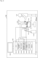
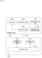
- Fig. 5 is a diagram illustrating an exemplary configuration of a ranging device according to an embodiment to which the present technology is applied.
- the reset transistor 254 may have a configuration in which the FD 253A and the FD 253B are individually provided, as illustrated in Fig. 7 , or may have configuration in which the FD 253A and the FD 253B are shared.
- the distribution of the charges in the pixel 250 will be described with reference to Fig. 8 .
- the distribution means reading of the charges accumulated in the pixel 250 (the PD 251) at a different timing and performing of the reading at each tap.
- a transfer control signal TRT1 controls ON/OFF of the transfer transistor 252A and a transfer control signal TRT2 controls ON/OFF of the transfer transistor 252B.
- the transfer control signal TRT1 has the same phase as the irradiation light
- the transfer control signal TRT2 has a phase inverted from that of the transfer control signal TRT1.
- the charges generated from the reflected light received by the PD 251 can be distributed to the taps 251A and 251B in accordance with the delay time Td, and the detection signals SIG1 and SIG2 can be output.
- the delay time Td corresponds to a time in which light emitted from the light-emitting unit 214 flies to an object and light reflected from the object flies to the light-receiving unit 212, that is, corresponds to a distance to the object.
- the ranging device 210 can obtain a distance (a depth) to the object in accordance with the delay time Td based on the detection signals SIG1 and SIG2.
- the transfer control signal TRT1 in the A frame, is turned on at the timing of the same phase (Phase0) as that of the irradiation light and the tap 251A starts receiving the light.
- the transfer control signal TRT2 is turned on at the timing of the phase (Phase 180) shifted by 180 degrees from that of the irradiation light and the tap 251B starts receiving the light.
- the taps 251A and 251B receive the light at the timing at which the phase is inverted by 180 degrees.
- charges accumulated in the FD 253A of the tap 251A at the timing of Phase0 at the irradiation time Tp are charges Q1 for a period of the A frame
- charges Q1' for an accumulation time of the irradiation time Tp within the period of the A frame are accumulated in the FD 253A for the period of the A frame.
- the charges Q1' accumulated in the FD 253A are read as a signal corresponding to the detection signal SIG1 from the FD 253A for a reading period.
- a signal value of the detection signal SIG1 corresponding to the charges Q1' is assumed to be a signal value I1.
- a shift amount ⁇ corresponding to the delay time Td can be detected at a distribution ratio of the signal values I1, I2, I3, and I4. That is, since the delay time Td is obtained based on the phase shift amount ⁇ , a distance to a target is obtained in accordance with the delay time Td.
- the phase shift amount ⁇ is obtained with the following Expression (1) and a distance D to the target is calculated with the following Expression (2).
- C denotes a velocity of light and Tp denotes a pulse width.
- ⁇ arctan I 1 ⁇ I 2 I 3 ⁇ I 4
- D ⁇ 2 ⁇ ⁇ T p C 2
- the ambient light when the ambient light is considered to be regular with respect to a pulse period and is thus regular light, the ambient light are superimposed as offset light equivalent to the signal values I1, I2, I3, and I4. Accordingly, a component (an offset component) of the ambient light in calculation of Expression (1) is cancelled out, and thus has no influence on a ranging result.
- the case of a TOF type sensor of the 2Tap-4Phase scheme has been described as an example.
- the present technology can also be applied to a TOF type sensor of another scheme.
- the TOF type sensor of the 4Tap-4Phase can also be applied.
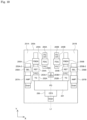
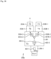
- FIG. 10 An exemplary planar configuration of the pixel 250 corresponding to the exemplary circuit example illustrated in Fig. 7 is illustrated in Fig. 10 .
- the pixel 250b illustrated in Fig. 10 will be described continuously as a pixel 250b in a second embodiment.
- a PD 261 is provided in a region near the central portion of the rectangular pixel 250a.
- a TG 252A and a TG 252B are provided on the upper side (upper side) of the PD 261 in the drawing.
- the TG 252A is a gate portion of the transfer transistor 252A and the TG 252B is a gate portion of the transfer transistor 252B.
- the TG 252A and the TG 252B are provided to be adjacent to one side among four sides of the PD 261.
- the TG 252A and the TG 252B are disposed side by side in the X axis direction of the upper side of the PD 261.
- An FD 253A-1 is provided on the upper side of the TG 252A.
- the FD 253A-1 configures a part of the FD 253A included in the tap 251A. That is, in the pixel 250b, the FD 253 is configured from two regions as in the pixel 20a (see Fig. 3 ) in the first embodiment.
- the FD 253A included in the tap 251A is configured from the FD 253A-1 and an FD 253A-2.
- the FD 253A-1 and the FD 253A-2 are formed in different regions.
- the FD 253A-1 is formed on the upper side of the TG 252A in the drawing and the FD 253A-2 is formed at a position away from the FD 253A-1 and a position on the upper side diagonally to the right of the FD 253A-1.
- the FD 253A-1 and the FD 253A-2 are connected by a wiring in a wiring layer and are treated as one region.
- An FDG 259A is formed on the upper side of the FD 253A-2 in the drawing.
- the additional capacitance unit 260A is formed on the upper side of the FDG 259A in the drawing.
- the amplification transistor 257A (its gate portion) included in the tap 251A is formed on the left side of the TG 252A in the drawing.
- the select transistor 258A (its gate portion) is formed on the upper side of the TG 252A in the drawing.
- the FBEN 255A is provided in the tap 251A.
- the FBEN 255A is formed on the upper side of the reset transistor 254A in the drawing.
- the FD 253A is distributed and formed in two regions of the FD 253A-1 and an FD 253A-2.
- the FD 253A-1 is connected to the RST 254A and the FBEN 255A is connected to the RST 254A.
- the FDG 259A is connected to the FD 253A-2.
- the FD 253A is divided and disposed in two regions of the FD 253A-1 and an FD 253A-2
- the FBEN 255A is connected to one of the FD 253A-1 and an FD 253A-2 through the RST 254A
- the FDG 259A is connected to the other thereof.
- Each unit forming the tap 251B is disposed on the right side of the tap 251Ain the drawing.
- the tap 251B has a configuration similar to the tap 251A.
- the TG 252B included in the tap 251B is formed on the upper right side of the PD 261 in the drawing.
- the FD 253B-1 is provided on the upper side of the TG 252B in the drawing.
- the FD 253B included in the tap 251B is configured from the FD 253B-1 and the FD 253B-2.
- the FD 253B-1 is formed on the upper side of the TG 252B in the drawing and the FD 253B-2 is formed at a position away from the FD 253B-1 and a position on the upper side diagonally to the left of the FD 253B-1.
- the FD 253B-1 and the FD 253B-2 are connected by a wiring in a wiring layer and are treated as one region.
- An FDG 259B is formed on the upper side of the FD 253B-2 in the drawing.
- the additional capacitance unit 260B is formed on the upper side of the FDG 259B in the drawing.
- the amplification transistor 257B (its gate portion) included in the tap 251B is formed on the right side of the TG 252B in the drawing.
- the select transistor 258B (its gate portion) is formed on the upper side of the TG 252B in the drawing.
- the FBEN 255B is provided in the tap 251B.
- the FBEN 255B is formed on the upper side of the reset transistor 254B in the drawing.
- a well contact 265 is provided on the upper side of the PD 261.
- a discharge transistor (OFG) 256 (its gate portion) is provided on the lower side of the PD 261.
- the discharge transistor 256 is an overflow gate for blooming prevention and is shared between the taps 251A and 251B. As illustrated in Fig. 10 , one OFD 256 is formed in the pixel 250b.
- Fig. 10 and the subsequent drawings The layout illustrated in Fig. 10 and the subsequent drawings is exemplary and does not mean limited description. In the examples given in Fig. 10 and the subsequent drawings, the configuration in which the discharge transistor 256 is provided has been described, but a configuration in which the discharge transistor 256 is not provided can also be used.
- each unit included in the tap 251A and each unit included in the tap 251B are linearly symmetric with respect to a central line L1 (a line L1 indicated by a dotted line in the drawing) of the pixel 250b.
- the TG 252A, the FD 253A-1, the FD 253A-2, the reset transistor 254A, the FBEN 255A, the amplification transistor 257A, the select transistor 258A, the FDG 259A, and the additional capacitance unit 260A included in the tap 251A are linearly symmetric to the TG 252B, the FD 253B-1, the FD 253B-2, the reset transistor 254B, the FBEN 255B, the amplification transistor 257B, the select transistor 258B, the FDG 259B, and the additional capacitance unit 260B included in the tap 251B, respectively.
- wirings are not illustrated, but the FD 253A-1 and the amplification transistor 257A are connected and a signal amount from the FD 253A-1 is supplied to the amplification transistor 257A.
- the FD 253B-1 and the amplification transistor 257B are connected and a signal amount from the FD 253B-1 is supplied to the amplification transistor 257B.
- a length of a wiring between the FD 253A-1 and the amplification transistor 257A can be substantially the same as a length of a wiring between the FD 253B-1 and the amplification transistor 257B.
- the other wirings have the same lengths by the wirings of the bilaterally symmetric targets.
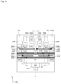
- Fig. 11 is a diagram illustrating an exemplary cross-sectional configuration of the pixel 250b including two taps 251 illustrated in Figs. 7 and 10 .
- the pixel 250b includes a semiconductor substrate 341 and a multilayer wiring layer 342 formed on the surface side (he lower side in the drawing).
- the semiconductor substrate 341 is formed of, for example, silicon (Si) and is formed with a thickness of, for example, about a few ⁇ m.
- an N-type (second conductive type) semiconductor region 352 is formed in unis of pixels in a P-type (first conductive type) semiconductor region 351, and the photodiode 261 is formed in units of pixels.
- the P-type semiconductor region 351 provided on the front and rear surfaces of the semiconductor substrate 341 serves as a hole or charge accumulation region for inhibiting a dark current.
- the upper surface of the semiconductor substrate 341 which is an upper side is the rear surface of the semiconductor substrate 341 and is a light incident surface on which light is incident.
- An antireflection film 343 is formed on the upper surface of the semiconductor substrate 341 on the rear surface side.
- the antireflection film 343 has a stacked structure in which a fixed charge film and an oxide film are stacked.
- An insulating thin film with a high dielectric constant (High-k) in conformity with, for example, an atomic layer deposition (ALD) method can be used.
- a hafnium oxide (HfO2), an aluminum oxide (Al2O3), a titanium oxide (TiO2), a strontium titan oxide (STO), or the like can be used.
- the antireflection film 343 is configured by stacking a hafnium oxide film 353, an aluminum oxide film 354, and a silicon oxide film 355.
- an inter-pixel light shielding film 345 that prevents incidence of incident light on an adjacent pixel is formed.
- a material of the inter-pixel light shielding film 345 may be a material that shields light.
- a metal material such as tungsten (W), aluminum (Al), or copper (Cu) can be used.
- a flattened film 346 is formed of an insulating film such as a silicon oxide (SiO2), a silicon nitride (SiN), a silicon oxynitride (SiON) or an organic material such as a resin.
- An on-chip lens 347 is formed in units of pixels on the upper surface of the flattened film 346.
- the on-chip lens 347 is formed of, for example, a resin material such as a styrene resin, an acrylic resin, a styrene-acrylic copolymer resin, or a siloxane resin. Light condensed by the on-chip lens 347 is efficiently incident on the PD 261.
- an inter-pixel separation unit 361 separating adjacent pixels from each other is formed from the rear surface side (the side of the on-chip lens 347) of the semiconductor substrate 341 until a predetermined depth in a substrate depth direction.
- An outer circumferential portion including the bottom surface and the sidewall of the inter-pixel separation unit 361 is covered with the hafnium oxide film 353 which is a part of the antireflection film 343.
- the inter-pixel separation unit 361 inhibits incident light from passing through the nearby pixels 250b to confine the incident light inside the self-pixels and inhibit leaking of incident light from the adjacent pixels 250b.
- a silicon oxide film 355 which is a material of the uppermost layer of the antireflection film 343 is buried in a trench (a groove) carved on the rear surface side, and thus the silicon oxide film 355 and the inter-pixel separation unit 361 are simultaneously formed. Therefore, the inter-pixel separation unit 361 and the silicon oxide film 355 which is a part of stacked films serving as the antireflection film 343 are formed of the same material, but may not be formed of the same material.
- a material with which the film is buried on the rear surface side serving as the inter-pixel separation unit 361 may be, for example, a metal material such as tungsten (W), aluminum (Al), titanium (Ti), or titanium nitride (TiN).
- two transfer transistors TRG1 and TRG2 are formed with respect to one PD 261 formed in each pixel 250b.
- the transfer transistor TRG1 corresponds to the TG 252A (see Fig. 10 ) and the transfer transistor TRG2 corresponds to the TG 252B (see Fig. 10 ).
- floating diffusion regions FD1 and FD2 serving as charge accumulation units that temporarily retain charges transferred from the PD 261 are formed from high-density N-type semiconductor regions (N-type diffusion regions).
- the floating diffusion region FD1 corresponds to the FD 253A (the FD 253A-1 or the FD 253A-2 (see Fig. 10 ) included in the FD 253A) and the floating diffusion region FD2 corresponds to the FD 253B (the FD 253B-1 or the FD 253B-2 (see Fig. 10 ) included in the FD 253B).
- the multilayer wiring layer 342 includes a plurality of wiring layers M and an inter-layer insulating film 362 therebetween.
- Fig. 11 illustrates an example in which four layers, wiring layers M1 to M4, are configured.
- Wirings 371 to 374 are respectively formed in the plurality of wiring layers M of the multilayer wiring layer 342.
- the wirings 371 to 374 are formed of, for example, metal films such as copper (Cu), aluminum (Al), tungsten (W), titanium (Ti), or titanium nitride (TiN).
- a wiring disposed in the wiring layer M1 is referred to as the wiring 371
- a wiring disposed in the wiring layer M2 is referred to as the wiring 372
- a wiring disposed in the wiring layer M3 is referred to as the wiring 373
- a wiring disposed in the wiring layer M4 is referred to as the wiring 374.
- the wirings 371 to 374 disposed in the wiring layers M1 to M4 are connected in necessary portions through a via 366 formed in the vertical direction.
- the pixel 250b has a rear surface irradiation type structure in which the semiconductor substrate 341 which is a semiconductor layer is disposed between the on-chip lens 347 and the multilayer wiring layer 342 and incident light is incident on the PD 261 from the rear surface side on which the on-chip lens 347 is formed.
- the pixel 250b has a configuration in which two transfer transistors TRG1 and TRG2 are included for the PD 261 provided in each pixel and charges (electrons) generated through photoelectric conversion in the PD 261 can be distributed to the floating diffusion regions FD1 and FD2.
- the FD 253A included in the tap 251A is formed in two regions of the FD 253A-1 and the FD 253A-2, and the two regions are connected by wirings.
- the wirings will be described with reference to Figs. 12 and 13 .
- the wirings are formed in the multilayer wiring layer 342 (see Fig. 11 ) stacked on the semiconductor substrate 341 in which the PD 261 is formed.
- Fig. 12 is a diagram illustrating the wiring of the wiring layer M1 added to the plan view of the pixel 250b illustrated in Fig. 10 .
- Fig. 13 is a diagram illustrating the wiring of the wiring layer M2 added to the plan view of the pixel 250b illustrated in Fig. 10 .
- the PD 261 and the TG 252A are connected by a wiring 431A formed in the wiring layer M1.
- a via 411A connected to the wiring layer M2 is formed on the lower side of the TG 252A in Fig. 12 which is the other end of the wiring 431A.
- a contact 412A connecting the TG 251A to the wiring 431A is formed on the lower side of the TG 251A in Fig. 12 which is the other end of the wiring 431A.
- connection includes physical connection and also includes connection in which charges or signals can be read despite non-physical connection.
- the via 411A is connected to the pixel driving line 246A formed in the wiring layer M2. Since the via 411A is connected to the wiring 431A (see Fig. 12 ) and the wiring 431 is connected to the TG 252A, the pixel driving line 246A is connected to the TG 251A.
- the pixel driving line 246A is a wiring through which a signal for driving the transfer transistor 252A is transferred.
- the FD 253A-2, the FD 253A-1, and the AMP 257A are connected by a wiring 432A.
- contacts 413A, 414A, and 415A are respectively formed. These contacts are connected to the wiring 432A.
- the wiring 432A can also be used as a region that configures the FD 253A. By lengthening a wiring length of the wiring 432A, it is possible to increase capacitance of the FD 253A. Accordingly, as illustrated in Fig. 13 , a wiring 441A configuring a part of the FD 253A is formed in the wiring layer M2. The wiring 441A is connected to the wiring 432A by the via 416A.
- the via 416A is formed between the TG 252A and the AMP 257Ain Figs. 12 and 13 .
- the wiring 432A is formed in the wiring layer M1 and the wiring 441A is formed in the wiring layer M2 to be connected to the via 416A.
- the wiring 441A is formed to increase the capacitance of the FD 253A and is not a wiring for connection, as described above. Therefore, the wiring 441A can be omitted.
- the example in which the wiring 441Ais formed in the wiring layer M2 will be described.
- the wiring 441A may be formed in the wiring layer M3 or the M4 other than the wiring layer M2.
- the wiring 433A is formed in regions corresponding to the lower side of the SEL 258A and the AMP 257A.
- the wiring 433A is connected to the via 417A formed in the SEL 258A and the contact 418A formed between the RST 254A and the FBEN 255A (a region corresponding to the drain of the reset transistor 254A).
- the wiring 433A is a portion corresponding to the parasitic capacitance C_ST in the circuit diagram illustrated in Fig. 7 .
- a wiring 434A is provided in the wiring layer M1, as illustrated in Fig. 12
- a wiring 442A is provided in the wiring layer M2, as illustrated in Fig. 13 .
- the portion corresponding to the parasitic capacitance C_ST is configured from the wirings 433A, 434A, and 442A.
- the wiring 433A formed in the wiring layer M1 is connected to the via 417A.
- the wiring 434A formed in the wiring layer M1 is connected to the via 419A.
- the wiring 442A formed in the wiring layer M2 is connected to the vias 417A and 419A. Accordingly, the wiring 433A, the via 417A, the wiring 442A, the via 419A, and the wiring 434A are formed in a connection state, and thus the parasitic capacitance C_ST is formed.
- the wiring 434A is formed as a wiring that extends from a region on the right side of the FD 253A-2 in the drawing to the OFD 256 through the lower side of the well contact 265 and the PD 261.
- the wirings related to the tap 251A are formed to be linearly symmetric to the wirings related to the tap 251B.
- the wirings related to the tap 251B will be described with reference to Figs. 12 and 13 .
- the PD 261 and the TG 252B are connected by a wiring 431B formed in the wiring layer M1.
- a via 411B connected to the wiring layer M2 is formed on the lower side of the TG 252B in Fig. 12 which is the other end of the wiring 431B.
- a contact 412B connecting the TG 251B to the wiring 431B is formed on the lower side of the TG 251B in Fig. 12 which is the other end of the wiring 431B.
- the via 411B is connected to the pixel driving line 246B formed in the wiring layer M2. Accordingly, the pixel driving line 246B is connected to the TG 251B.
- the pixel driving line 246B is a wiring through which a signal for driving the transfer transistor 252B is transferred.
- the FD 253B-1, the FD 253B-2, and the AMP 257B are connected by a wiring 432B.
- contacts 413B, 414B, and 415B are respectively formed. These contacts are connected to the wiring 432B.
- a wiring 441B configuring a part of the FD 253B is formed in the wiring layer M2.
- the wiring 441B is connected to the wiring 432B by the via 416B.
- the wiring 433B is formed in regions corresponding to the lower side of the SEL 258B and the AMP 257B.
- the wiring 433B is connected to the via 417B formed in the SEL 258B and the contact 418B formed between the RST 254B and the FBEN 255B (a region corresponding to the drain of the reset transistor 254B).
- the wiring 433B formed in the wiring layer M1 is connected to the via 417B.
- the wiring 434B formed in the wiring layer M1 is connected to the via 419B.
- the wiring 442B formed in the wiring layer M2 is connected to the via 417B and the via 419B. Accordingly, the wiring 433B, the via 417B, the wiring 442B, the via 419B, and the wiring 434B are formed in a connection state, and thus the parasitic capacitance C_ST is formed.
- the wiring 434B is formed as a wiring that extends from a region on the right side of the FD 253B-2 in the drawing to the OFD 256 through the lower side of the well contact 265 and the PD 261.
- the wirings related to the tap 251B are formed to be linearly symmetric to the wirings related to the tap 251A.
- the transistors, the wirings, and the like included in the tap 251A included in the pixel 250b and the transistors, the wirings, and the like included in the tap 251B included in the pixel 250b are disposed to be linearly symmetric along the central line L1 (see Fig. 10 ) in the pixel 250b.
- the length of the wiring contributing to noise cancellation for example, the length of the wiring 433, the wiring 434, or the like corresponding to, for example, the parasitic capacitance C_ST, can be inhibited from varying. Accordingly, it is possible to inhibit difference in the performance related to noise reduction between the taps 251A and 251B, and thus it is possible to improve a ranging system.
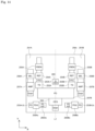
- FIG. 14 is a diagram illustrating an exemplary planar configuration of the pixel 250c according to the third embodiment.
- An exemplary circuit configuration of the pixel 250c according to the third embodiment is the same as the exemplary circuit configuration of the pixel 250 illustrated in Fig. 7 .
- An exemplary cross-sectional configuration of the pixel 250c according to the third embodiment can be the same as the exemplary cross-sectional configuration of the pixel 250b illustrated in Fig. 11 .
- description of the circuit configuration and the cross-sectional configuration will be omitted.
- the same reference numerals are given to the same portions as those of the pixel 250b in the second embodiment illustrated in Fig. 10 , and description thereof will be appropriately omitted.
- the pixel 250c differs in that an FDG 259Ac and an FDG 259Bc are provided on the lower side of the PD 261 in the drawing.
- the FDG 259Ac and the FDG 259Bc are moved to the lower side of the PD 261, and thus an FD 253A-2c connected to the FDG 259Ac and an FD 253B-2c connected to the FDG 259Bc are also disposed on the lower side.
- an additional capacitance unit 260Ac connected to the FDG 259Ac and an additional capacitance unit 260Bc connected to the FDG 259Bc are also disposed on the lower side.
- the FD 253A-2c, the FDG 259Ac, and the additional capacitance unit 260Ac are disposed side by side in the drawing.
- the FD 253B-2c, the FDG 259Bc, and the additional capacitance unit 260Bc are disposed side by side in the drawing.
- the FD 253A-2c, the FDG 259Ac, and the additional capacitance unit 260Ac and the FD 253B-2c, the FDG 259Bc, and the additional capacitance unit 260Bc are disposed to be linearly symmetric with respect to the central line L1.
- each unit included in the tap 251A and each unit included in the tap 251B are disposed to be linearly symmetric as in the pixel 250b illustrated in Fig. 10 .
- the wirings included in the tap 251A and the wirings included in the tap 251B are disposed to be linearly symmetric as in the pixel 250b in the second embodiment.
- the transistors, the wirings, and the like included in the tap 251A included in the pixel 250c and the transistors, the wirings, and the like included in the tap 251B included in the pixel 250c can be disposed to be linearly symmetric with respect to the central line L1 (see Fig. 14 ) in the pixel 250c. Accordingly, for example, it is possible to inhibit a variation in the wiring contributing to noise cancellation, for example, the wiring or the like corresponding to the parasitic capacitance C_ST.
- FIG. 15 is a diagram illustrating an exemplary planar configuration of the pixel 250d according to the fourth embodiment.
- An exemplary circuit configuration of the pixel 250d according to the fourth embodiment is the same as the exemplary circuit configuration of the pixel 250 illustrated in Fig. 7 .
- An exemplary cross-sectional configuration of the pixel 250c according to the fourth embodiment can be the same as the exemplary cross-sectional configuration of the pixel 250b illustrated in Fig. 11 .
- description of the circuit configuration and the cross-sectional configuration will be omitted.
- the same reference numerals are given to the same portions as those of the pixel 250b in the second embodiment illustrated in Fig. 10 , and description thereof will be appropriately omitted.
- the pixel 250d differs in that an FDG 259Ad and an FDG 259Bd are provided on the lower side of the PD 261 in the drawing.
- the pixel 250d illustrated in Fig. 15 is compared to the pixel 250c illustrated in Fig. 14 , the pixel 250d is the same in that the FDG 259Ad and the FDG 259Bd are provided on the lower side of the PD 261 in the drawing.
- the pixel 250d differs in that an FD 253A-2d, an FDG 259Ad, and an additional capacitance unit 260Ad are disposed in the vertical direction in the drawing and an FD 253B-2d, an FDG 259Bd, and an additional capacitance unit 260Bd are disposed in the vertical direction in the drawing.
- the position of the FBEN 255 is disposed at a position different from the pixels 250b and 250c.
- the FDG 259 and the like are disposed on the lower side of the PD 261, and thus the FBEN 255 and the like can be disposed in regions where the FDG 259 and the like are disposed.
- Fig. 15 illustrates a case in which the FBEN 255A and the FBEN 255B are disposed on the upper side in the drawing and the FBEN 255A and the FBEN 255B are formed in the horizontal direction.
- the position of the FBEN 255Ac is disposed in the middle side and the upper side of the pixel 250d, the position of the RST 254A is shifted on the upper side so that a region between the RST 254A and the TG 252A, that is, a region corresponding to the FD 253A-1, may be widely formed.
- each unit included in the tap 251A and each unit included in the tap 251B are disposed to be linearly symmetric as in the pixel 250b illustrated in Fig. 10 .
- the wirings included in the tap 251A and the wirings included in the tap 251B are disposed to be linearly symmetric as in the pixel 250b in the second embodiment.
- the transistors, the wirings, and the like included in the tap 251A included in the pixel 250d and the transistors, the wirings, and the like included in the tap 251B included in the pixel 250d can be disposed to be linearly symmetric with respect to the central line L1 (see Fig. 15 ) in the pixel 250d. Accordingly, for example, it is possible to inhibit a variation in the wiring contributing to noise cancellation, for example, the wiring or the like corresponding to a parasitic capacitance D_ST.
- the disposition and the sizes are exemplary.
- the present technology can be applied despite disposition and sizes other than the disposition and the sizes given in the examples.
- the pixel to which the present technology is applied can be treated as one FD by distributing and disposing a region serving as a floating diffusion region (FD) in two regions and connecting the two regions.
- the FD is distributed and disposed in two regions, and thus the degree of disposition can be increased.
- By distributing and disposing the FD in two regions it is also possible to form the FD as a region larger than when the FD is provided in one region.
- the FD 253A is formed in two regions, for example, the FD 253A-1 and the FD 253A-2 in the pixel 250b illustrated in Fig. 10 , has been described as an example.
- the FD may be divided and provided in two or more regions.
- the TG 252, the FD 253, and the OFG 256 are disposed to be linearly symmetric.
- the disposition and the number of TGs 252, FDs 253, and OFGs 256 may be position and the number thereof other than in the example illustrated in Fig. 16 or may be disposition examples or numbers to be described below.
- Fig. 17 is a diagram illustrating an exemplary configuration of a pixel 250e according to a fifth embodiment.
- the pixel 250e illustrated in Fig. 17 differs from the pixel 250 illustrated in Fig. 16 in that two OFDs 256 are provided.
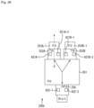
- the OFD 256-1 and the OFD 256-2 are disposed side by side in the X axis direction of the lower side of the PD 261.
- the OFD 256-1 and the OFD 256-2 are disposed to be linearly symmetric with respect to the central line L1 of the pixel 250.
- the OFDs 256 are configured to be linearly symmetric with reference to the central line L1 as in the TG 252.
- the OFDs 256 are configured to be linearly symmetric with reference to the central line L1 as in the TG 252.
- the pixel 250f illustrated in Fig. 18 is the same in that the two OFDs 256 are provided, but differs in positions at which the OFDs 256 are disposed.
- the TG 252 and the OFG 256 are not disposed on the opposite sides.
- the OFG 256 is disposed at a position close to the TG 252.
- the TG 252 and the OFG 256 are disposed at positions at which the TG 252 and the OFG 256 form a right angle. In this way, the TG 252 and the OFG 256 are disposed at positions which are not opposite, and thus charge transfer directions are not opposite. It is possible to implement a configuration in which a difference occurring between a transmission speed at which the charges are transmitted to the TG 252 and a transfer speed at which the charges are transmitted to the OFG 256 is prevented.
- the pixel 250f illustrated in Fig. 18 is the same in that the two OFDs 256 are provided, but differs in positions at which the OFDs 256 are disposed.
- the TG 252A, the TG 252B, the OFD 256-1, and the OFD 256-2 are disposed on the upper side of the PD 261.
- the TG 252A, the FD 253A-1, and the OFG 256-1, and the TG 252B, the FD 253B-1, and the OFG 256-2 are disposed to be linearly symmetric with reference to the central line L1 of the pixel 250g.
- the TG 252 and the OFG 256 are disposed in a predetermined one side of the PD 261 and charge transfer directions can be aligned in a direction in which the one side is located.
- By aligning the charge transfer directions in one direction for example, it is easy to design a potential gradient as gradient oriented in the direction. A difference occurring between a transmission speed at which the charges are transmitted to the TG 252 and a transfer speed at which the charges are transmitted to the OFG 256 is prevented.
- Fig. 20 is a diagram illustrating an exemplary planar configuration of a pixel 250h according to an eighth embodiment.
- the TG 252A, the OFG 256, and the TG 252B are disposed in order in the X axis direction of the upper side of the PD 261.
- the OFG 256 is located on the central line L1 of the pixel 250h, and the TG 252A and the TG 252B are disposed on both sides of the OFG 256.
- the TGs 252 and the OFG 256 are disposed in one side. Therefore, as in the pixel 250g (see Fig. 19 ), it is possible to improve a charge transfer capability of the TG 252 and it is possible to improve a charge discharge capability of the OFG 256.
- Fig. 21 is a diagram illustrating an exemplary planar configuration of a pixel 250i according to a ninth embodiment.
- the pixel 250 according to the first to eighth embodiments is a pixel that has the 2-tap configuration and the configuration in which two TGs 252 are provided has been described as an example.
- a pixel can have a 4-tap configuration.
- four TGs 252 are provided.
- a TG 252A-2, a TG 252A-1, a TG 252B-1, and a TG 252B-2 are disposed in order from the left in the X axis direction of the upper side of the PD 261.
- Fig. 22 is a diagram illustrating a shape of a gate in a plan view.
- TG 252 or the OFG 256 in which the shape of the gate is rectangular has been described.
- a shape other than a rectangle may be used.
- Fig. 22 illustrates an example of a configuration in which the shape of the gate is a gate that has a shape other than a rectangle in the configuration of the pixel 250 illustrated in Fig. 16 .
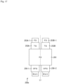
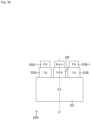
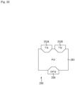
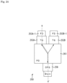
- the TG 252A, the TG 252B, and the OFG 256 are each hexagonal. In other words, corners of the rectangular gate are cut off in the shape. In this way, by cutting off the corners in the shape of the gate, it is possible to reduce gate capacitance and it is possible to improve a transfer capability.
- the charge transfer directions can be aligned in one direction. It is possible to improve a charge transfer capability of the TG 252 and it is possible to improve a charge discharge capability of the OFG 256.
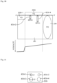
- Fig. 24 is a diagram illustrating the pixel 250 illustrated in Fig. 16 in a plan view again.
- Fig. 25 is a diagram illustrating a cross-sectional configuration taken along the line A-A' in the plan view of the pixel 250 illustrated in Fig. 24 .
- the PD 261 is provided in a Pwell region 401 formed from a silicon (Si) substrate.
- the PD 261 has a structure in which, for example, an N-type impurity layer (a charge accumulation layer) is formed and a high-density P-type impurity layer which is a depletion prevention layer (a pinning layer) is formed above the N-type impurity layer.
- an N-type impurity layer a charge accumulation layer
- a high-density P-type impurity layer which is a depletion prevention layer (a pinning layer) is formed above the N-type impurity layer.
- the FD 253A-1 that accumulates charges generated in the PD 61 is provided.
- the TG 252A is provided between the PD 261 and the FD 253A-1.
- the OFD 256 is provided.
- the charges generated in the PD 261 are distributed to the TG 252A included in the tap 251A and the TG 252B included in the tap 251B at a timing at which the TG 252A or the TG 252B is turned on or off.
- the charges can also be discharged by the OFG 256 for discharging. That is, the charges generated in the PD 261 are distributed in one of three different directions at a timing at which the gate is turned on or off.
- the TG 252 may be a vertical gate transistor.
- the vertical gate transistor it is possible to increase potential modulation in the Pwell region 401 formed from a silicon (Si) substrate, and thus it is possible to improve the charge distribution capability to the TG 252A and the TG 252B.
- a reset capability of the PD 261 can be added.
- Fig. 26 is a plan view illustrating an exemplary configuration of a pixel 250j according to a tenth embodiment.
- Fig. 27 is a cross-sectional view illustrating a cross-sectional configuration taken along the line A-A' in the plan view of the pixel 250j in Fig. 26 .
- the pixel 250j illustrated in Fig. 26 includes a vertical gate unit 421A in the TG 252A, includes a vertical gate unit 421B in the TG 252B, and includes a vertical gate unit 422 in the OFG 256.
- the TG 252A includes the vertical gate unit 421A.
- the vertical gate unit 421A is a portion formed as a transfer gate in which a vertical transistor trench is opened and charges are read from the PD 261.
- the TG 252A is a transfer gate electrode in which a planar gate electrode and a vertical gate electrode are integrated.
- the vertical gate electrode is referred to as the vertical gate unit 421A herein.
- the TG 252B includes a planar gate electrode and the vertical gate unit 421B as in the TG 252A.
- the OFG 256 includes a planar gate electrode and the vertical gate unit 422 as in the TG 252A.
- the TG 253 as a vertical transistor that includes the vertical gate unit 421, it is possible to efficiently read the charges from a deep portion of the PD 261. It is possible to transfer the charges generated through photoelectric conversion in the PD 261 distributed at a high speed at a potential gradient by the vertical gate unit 422.
- the vertical gate unit 421 can become robust without being influenced.
- a charge discharge function can be added.
- the vertical gate unit 422 even in the OFG 256, it is possible to further inhibit the charges remaining in the PD 261 due to a transfer failure than in a case in which the charges are detected as signal component through the TG 252A and the TG 252B.
- the configuration of the gate including the vertical gate unit can also be applied to gates of other transistors.
- Fig. 28 is a plan view illustrating an exemplary configuration of a pixel 250k according to an eleventh embodiment.
- the plurality of vertical gate units may be provided per gate.
- Fig. 28 is a diagram illustrating an exemplary configuration of a pixel 250k including two vertical gate units per gate.
- the vertical gate unit 421A-1 and the vertical gate unit 421A-2 are disposed side by side in the left and right directions (the X axis direction) in the drawing.
- the vertical gate unit 421B-1 and the vertical gate unit 421B-2 are disposed side by side in the left and right directions in the drawing.
- the vertical gate unit 422-1 and the vertical gate unit 422-2 are disposed side by side in the left and right directions in the drawing.
- two vertical gate units 421 may be included in one TG 252.
- the two vertical gate units 421 disposed side by side in the TG 252 may be in the foregoing X axis direction or the Y axis direction (the upward and downward directions in the drawing).
- the other gates can include two vertical gate units as in the TG 252.
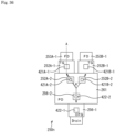
- FIG. 29 an exemplary configuration of a pixel 250k' in which four vertical gate units 421 are included in one TG 252 is illustrated.
- vertical gate units 421A-1 to 421A-4 are disposed in four corners of the TG 252A.
- vertical gate units 421B-1 to 421B-4 are disposed in four corners of the TG 252B.
- vertical gate units 422-1 to 422-4 are disposed in four corners of the OFG 256.
- four vertical gate units 421 may be included in one TG 252. In the other gates, four vertical gate units can be included as in the TG 252.
- a plurality of vertical gate units other than two or four vertical gate units can also be included in one gate.
- the disposition of the vertical gate units may be disposition other than the side-by-side disposition in which the vertical gate units are disposed in, for example, four corners of the gate in the foregoing predetermined direction in accordance with the shape of the gate.
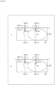
- Fig. 30 is a cross-sectional view illustrating a cross-sectional configuration taken along the line A-A' in the plan view of the pixel 250k' in Fig. 29 .
- the vertical gate units 421A-1 to 421A-4 provided in the TG 252A, the vertical gate units 421A-2 and 421A-4 disposed on a straight line (the line A-A') connecting the FD 253A-1 to the PD 261 are illustrated.
Landscapes
- Engineering & Computer Science (AREA)
- Multimedia (AREA)
- Signal Processing (AREA)
- Physics & Mathematics (AREA)
- Computer Networks & Wireless Communication (AREA)
- General Physics & Mathematics (AREA)
- Radar, Positioning & Navigation (AREA)
- Remote Sensing (AREA)
- Electromagnetism (AREA)
- Solid State Image Pick-Up Elements (AREA)
- Transforming Light Signals Into Electric Signals (AREA)
Claims (12)
- Bildgebungselement, umfassend:eine photoelektrische Umwandlungseinheit (51), die konfiguriert ist, um eine photoelektrische Umwandlung durchzuführen;eine Ladungsakkumulationseinheit (53), die konfiguriert ist, um Ladungen, die durch die photoelektrische Umwandlungseinheit (51) erhalten werden, zu akkumulieren;eine Übertragungseinheit (52), die konfiguriert ist, um die Ladungen von der photoelektrischen Umwandlungseinheit (51) zu der Ladungsakkumulationseinheit (53) zu übertragen;eine Rücksetzeinheit (54), die konfiguriert ist, um die Ladungsakkumulationseinheit (53) rückzusetzen;eine Rücksetzspannungssteuereinheit (55), die konfiguriert ist, um eine Rücksetzspannung, die an die Rücksetzeinheit (54) angelegt werden soll, zu steuern; undeine zusätzliche Steuereinheit (59), die konfiguriert ist, um eine Hinzufügung von Kapazität (60) zu der Ladungsakkumulationseinheit (53) zu steuern,wobei die Ladungsakkumulationseinheit (53) eine Vielzahl von Regionen (53-2-4, 53-1-3) einschließt,wobei die Vielzahl von Regionen (53-2-4, 53-1-3), die in der Ladungsakkumulationseinheit (53) eingeschlossen sind, in einem Substrat (341) bereitgestellt sind, in dem die photoelektrische Umwandlungseinheit (51) bereitgestellt ist,wobei erste Verdrahtungen (431, 432), die die Vielzahl von Regionen (53-2-4, 53-1-3) verbinden, in einer ersten Verdrahtungsschicht (M1), die auf dem Substrat (341) gestapelt ist, bereitgestellt sind,wobei zweite Verdrahtungen (441), die einige der Ladungsakkumulationseinheiten (53) ausbilden, in einer zweiten Schicht (M2), die sich von der ersten Schicht (M1) unterscheidet, bereitgestellt sind, in der die ersten Verdrahtungen (431, 432), die die Vielzahl von Regionen (53-2-4, 53-1-3) verbinden, bereitgestellt sind, undwobei, in der ersten Verdrahtungsschicht (M1) und der zweiten Verdrahtungsschicht (M2) dritte Verdrahtungen (433, 434, 442) bereitgestellt sind, wobei eine erste (433) der dritten Verdrahtungen (433, 434, 442) in der ersten Verdrahtungsschicht (M1) ausgebildet und mit einem ersten Durchgangsloch (417) und einem Kontakt (418), der zwischen der Rücksetzeinheit (54) und der Rücksetzspannungssteuereinheit (55) ausgebildet ist, verbunden ist, eine zweite (434) der dritten Verdrahtungen (433, 434, 442) in der ersten Verdrahtungsschicht (M1) ausgebildet und mit einem zweiten Durchgangsloch (419) verbunden ist, und eine dritte (442) der dritten Verdrahtungen (433, 434, 442) in der zweiten Verdrahtungsschicht (M2) ausgebildet und mit dem ersten Durchgangsloch (417) und dem zweiten Durchgangsloch (419) verbunden ist, undwobei die erste (433) der dritten Verdrahtungen (433, 43, 442), das erste Durchgangsloch (417), die dritte (442) der dritten Verdrahtungen (433, 434, 442), das zweite Durchgangsloch (419) und die zweite (434) der dritten Verdrahtungen (433, 434, 442) eine parasitäre Kapazität (C_ST) mit Erdung an dem Kontakt (418) ausbilden, der zwischen der Rücksetzeinheit (54) und der Rücksetzspannungssteuereinheit (55) ausgebildet ist.
- Bildgebungselement nach Anspruch 1, wobei die Vielzahl von Regionen (53-2-4, 53-1-3) zwei Regionen sind, eine der Regionen (53-2-4) in einem ersten Pixel (20a-4) bereitgestellt ist und die andere Region (53-1-3) in einem zweiten Pixel (20a-3) angrenzend an das erste Pixel (20a-4) bereitgestellt ist.
- Bildgebungselement nach einem der vorstehenden Ansprüche, wobei, von der Vielzahl von Regionen (53-2-4, 53-1-3), die in der Ladungsakkumulationseinheit (53) eingeschlossen sind, eine Region (53-2-4, 53-1-3) mit der Übertragungseinheit (52) verbunden ist und eine andere Region (53-2-4, 53-1-3) mit der zusätzlichen Steuereinheit (59) verbunden ist.
- Bildgebungselement nach Anspruch 3, wobei eine Vielzahl von Ladungsakkumulationseinheiten (53), eine Vielzahl von Übertragungseinheiten (52), eine Vielzahl von Rücksetzeinheiten (54), eine Vielzahl von Rücksetzspannungssteuereinheiten (55) und eine Vielzahl von zusätzlichen Steuereinheiten (59) linear symmetrisch sind.
- Bildgebungselement nach Anspruch 4, ferner umfassend:eine Entladungseinheit (56), die konfiguriert ist, um Ladungen, die durch die photoelektrische Umwandlungseinheit (51) erhalten werden, zu entladen,wobei die Entladungseinheit (56) linear symmetrisch ist.
- Bildgebungselement nach Anspruch 5, wobei die Entladungseinheit (56) an einer Position, an der die Entladungseinheit (56) mit der Übertragungseinheit (52) einen rechten Winkel ausbildet, angeordnet ist, oder wobei die Entladungseinheit (56) und die Übertragungseinheit (52) nebeneinander auf einer Seite der photoelektrischen Umwandlungseinheit (51) angeordnet sind.
- Bildgebungselement nach einem der vorstehenden Ansprüche,wobei die Übertragungseinheit (52) ein vertikales Gate einschließt, odereine Vielzahl von den vertikalen Gates einschließt, undwobei sich die Tiefen der vertikalen Gates unterscheiden.
- Bildgebungselement nach einem der vorstehenden Ansprüche,wobei die Übertragungseinheit (52) ein erstes und ein zweites Gate einschließt, undwobei das erste Gate zwischen der photoelektrischen Umwandlungseinheit (51) und der Ladungsakkumulationseinheit (53) angeordnet ist und das zweite Gate an einer Position, die über der photoelektrischen Umwandlungseinheit (51) liegt, angeordnet ist.
- Bildgebungselement nach Anspruch 8, wobei mindestens eines des ersten und des zweiten Gates ein vertikales Gate ist.
- Bildgebungselement nach Anspruch 9, wobei das erste und das zweite Gate gleichzeitig angesteuert werden.
- Bildgebungsvorrichtung (10), umfassend:ein Bildgebungselement nach einem der vorstehenden Ansprüche; undeine Verarbeitungseinheit (28), die konfiguriert ist, um ein Signal von dem Bildgebungselement zu verarbeiten.
- Entfernungsmessvorrichtung (210), umfassend:eine Lichtemissionseinheit (214), die konfiguriert ist, um Strahlungslicht zu emittieren; undein Lichtempfangselement (212), das konfiguriert ist, um reflektiertes Licht zu empfangen, wenn Licht von der Lichtemissionseinheit (214) von einem Objekt reflektiert wird,wobei das Lichtempfangselement (212) das Bildgebungselement nach einem der Ansprüche 1 bis 10 einschließt.
Applications Claiming Priority (2)
| Application Number | Priority Date | Filing Date | Title |
|---|---|---|---|
| JP2020012436 | 2020-01-29 | ||
| PCT/JP2021/002376 WO2021153480A1 (ja) | 2020-01-29 | 2021-01-25 | 撮像素子、撮像装置、測距装置 |
Publications (3)
| Publication Number | Publication Date |
|---|---|
| EP4099685A1 EP4099685A1 (de) | 2022-12-07 |
| EP4099685A4 EP4099685A4 (de) | 2023-04-26 |
| EP4099685B1 true EP4099685B1 (de) | 2025-02-26 |
Family
ID=77078220
Family Applications (1)
| Application Number | Title | Priority Date | Filing Date |
|---|---|---|---|
| EP21747394.1A Active EP4099685B1 (de) | 2020-01-29 | 2021-01-25 | Bildgebendes element, bildgebende vorrichtung und abstandsmessvorrichtung |
Country Status (7)
| Country | Link |
|---|---|
| US (1) | US12149845B2 (de) |
| EP (1) | EP4099685B1 (de) |
| JP (1) | JP7615059B2 (de) |
| KR (1) | KR20220133873A (de) |
| CN (1) | CN114946172B (de) |
| TW (1) | TWI882059B (de) |
| WO (1) | WO2021153480A1 (de) |
Families Citing this family (6)
| Publication number | Priority date | Publication date | Assignee | Title |
|---|---|---|---|---|
| KR20220133879A (ko) * | 2020-01-29 | 2022-10-05 | 소니 세미컨덕터 솔루션즈 가부시키가이샤 | 촬상 소자, 거리 측정 모듈 |
| KR20220158109A (ko) * | 2021-05-20 | 2022-11-30 | 삼성전자주식회사 | 깊이 센서 및 그 동작 방법 |
| JP2023055062A (ja) * | 2021-10-05 | 2023-04-17 | ソニーセミコンダクタソリューションズ株式会社 | 固体撮像装置 |
| EP4451006A4 (de) * | 2021-12-23 | 2025-09-10 | Univ Shizuoka Nat Univ Corp | Abstandsbildmessvorrichtung und abstandsbildmessverfahren |
| WO2024071091A1 (ja) * | 2022-09-27 | 2024-04-04 | ヌヴォトンテクノロジージャパン株式会社 | 撮像装置、測距装置及び撮像装置の制御方法 |
| CN120143170A (zh) * | 2023-12-13 | 2025-06-13 | 晶相光电股份有限公司 | 控制装置及其操作方法 |
Family Cites Families (25)
| Publication number | Priority date | Publication date | Assignee | Title |
|---|---|---|---|---|
| JP4117540B2 (ja) | 2002-10-17 | 2008-07-16 | ソニー株式会社 | 固体撮像素子の制御方法 |
| JP2006108497A (ja) * | 2004-10-07 | 2006-04-20 | Matsushita Electric Ind Co Ltd | 固体撮像装置 |
| US7705900B2 (en) * | 2005-06-01 | 2010-04-27 | Eastman Kodak Company | CMOS image sensor pixel with selectable binning and conversion gain |
| EP2079229B1 (de) * | 2008-01-10 | 2011-09-14 | Stmicroelectronics Sa | Pixelschaltung für globalen elektrischen Verschluss |
| US8446010B2 (en) * | 2008-04-25 | 2013-05-21 | Sharp Kabushiki Kaisha | Multilayer wiring, semiconductor device, substrate for display device, and display device |
| JP5431771B2 (ja) * | 2009-04-07 | 2014-03-05 | 浜松ホトニクス株式会社 | 固体撮像装置 |
| JP5348176B2 (ja) * | 2011-05-16 | 2013-11-20 | ソニー株式会社 | 固体撮像装置、固体撮像装置の駆動方法、及び電子機器 |
| US9426397B2 (en) | 2013-11-12 | 2016-08-23 | EO Vista, LLC | Apparatus and methods for hyperspectral imaging with on-chip digital time delay and integration |
| US9584800B2 (en) * | 2014-03-31 | 2017-02-28 | Semiconductor Components Industries, Llc | Imaging systems with pixel array verification circuitry |
| CN105934826B (zh) * | 2014-12-18 | 2021-07-20 | 索尼公司 | 固态图像传感器、成像装置和电子设备 |
| JP2017163010A (ja) * | 2016-03-10 | 2017-09-14 | ソニー株式会社 | 撮像装置、電子機器 |
| JP2017175345A (ja) * | 2016-03-23 | 2017-09-28 | ソニー株式会社 | 固体撮像装置、固体撮像装置の駆動方法、及び、電子機器 |
| US9936153B1 (en) * | 2016-10-04 | 2018-04-03 | Omnivision Technologies, Inc. | CMOS image sensor with dual floating diffusions per pixel for flicker-free detection of light emitting diodes |
| US11025846B2 (en) * | 2017-02-01 | 2021-06-01 | Sony Semiconductor Solutions Corporation | Imaging system, imaging apparatus, and control apparatus |
| JP2018186398A (ja) * | 2017-04-26 | 2018-11-22 | ソニーセミコンダクタソリューションズ株式会社 | 固体撮像装置、および電子機器 |
| CN117577652A (zh) | 2017-06-02 | 2024-02-20 | 索尼半导体解决方案公司 | 固态摄像装置和电子设备 |
| KR102432861B1 (ko) * | 2017-06-15 | 2022-08-16 | 삼성전자주식회사 | 거리 측정을 위한 이미지 센서 |
| KR102673020B1 (ko) * | 2018-04-04 | 2024-06-05 | 소니 세미컨덕터 솔루션즈 가부시키가이샤 | 고체 촬상 장치 |
| JP2019191018A (ja) * | 2018-04-26 | 2019-10-31 | ソニー株式会社 | 測距装置及び測距モジュール |
| DE112019002463T5 (de) * | 2018-05-16 | 2021-04-22 | Sony Semiconductor Solutions Corporation | Festkörperbildgebungselement und festkörperbildgebungsvorrichtung |
| CN112119500B (zh) * | 2018-05-21 | 2025-06-17 | 索尼公司 | 固态摄像元件及其制造方法 |
| JP2019216379A (ja) | 2018-06-14 | 2019-12-19 | ソニーセミコンダクタソリューションズ株式会社 | 固体撮像素子、撮像装置、および、固体撮像素子の制御方法 |
| JP7175655B2 (ja) | 2018-07-18 | 2022-11-21 | ソニーセミコンダクタソリューションズ株式会社 | 受光素子および測距モジュール |
| JP7362198B2 (ja) * | 2018-07-18 | 2023-10-17 | ソニーセミコンダクタソリューションズ株式会社 | 受光素子、測距モジュール、および、電子機器 |
| CN110168398B (zh) * | 2018-07-18 | 2023-05-12 | 深圳市汇顶科技股份有限公司 | 飞时测距系统及校正方法 |
-
2021
- 2021-01-08 TW TW110100720A patent/TWI882059B/zh active
- 2021-01-25 JP JP2021574008A patent/JP7615059B2/ja active Active
- 2021-01-25 KR KR1020227023917A patent/KR20220133873A/ko not_active Abandoned
- 2021-01-25 US US17/759,118 patent/US12149845B2/en active Active
- 2021-01-25 CN CN202180008149.2A patent/CN114946172B/zh active Active
- 2021-01-25 EP EP21747394.1A patent/EP4099685B1/de active Active
- 2021-01-25 WO PCT/JP2021/002376 patent/WO2021153480A1/ja not_active Ceased
Also Published As
| Publication number | Publication date |
|---|---|
| JP7615059B2 (ja) | 2025-01-16 |
| JPWO2021153480A1 (de) | 2021-08-05 |
| TW202133424A (zh) | 2021-09-01 |
| EP4099685A4 (de) | 2023-04-26 |
| US12149845B2 (en) | 2024-11-19 |
| KR20220133873A (ko) | 2022-10-05 |
| EP4099685A1 (de) | 2022-12-07 |
| US20230044912A1 (en) | 2023-02-09 |
| CN114946172A (zh) | 2022-08-26 |
| WO2021153480A1 (ja) | 2021-08-05 |
| TWI882059B (zh) | 2025-05-01 |
| CN114946172B (zh) | 2026-03-20 |
Similar Documents
| Publication | Publication Date | Title |
|---|---|---|
| EP4099685B1 (de) | Bildgebendes element, bildgebende vorrichtung und abstandsmessvorrichtung | |
| US20210082974A1 (en) | Imaging element | |
| US12316987B2 (en) | Solid-state imaging device | |
| TWI857044B (zh) | 成像元件及距離測量裝置 | |
| US20250016464A1 (en) | Solid-state imaging device and electronic device | |
| US20250133847A1 (en) | Imaging apparatus and electronic device | |
| CN114631187B (zh) | 固态成像装置和电子设备 | |
| JP2023003799A (ja) | 固体撮像装置 | |
| US20220344390A1 (en) | Organic cis image sensor | |
| US12027538B2 (en) | Imaging element and electronic apparatus | |
| US20250194274A1 (en) | Photodetection apparatus | |
| US20260082714A1 (en) | Photodetection device and electronic apparatus | |
| US20250133845A1 (en) | Photodetector and electronic apparatus | |
| EP4447115A1 (de) | Photodetektor und elektronisches gerät | |
| US20240313014A1 (en) | Imaging apparatus and electronic device | |
| JP7275125B2 (ja) | 撮像素子、電子機器 | |
| US20210114988A1 (en) | Photoelectric conversion element | |
| US20260090117A1 (en) | Imaging device and electronic apparatus | |
| US20240387593A1 (en) | Solid-state imaging device | |
| EP4712141A1 (de) | Halbleiteranordnung | |
| US20250194273A1 (en) | Photodetection apparatus | |
| KR20250136838A (ko) | 반도체 장치 | |
| WO2025134554A1 (ja) | 固体撮像装置 | |
| WO2023021740A1 (ja) | 撮像素子、撮像装置、製造方法 | |
| CN121400093A (zh) | 光检测装置和电子设备 |
Legal Events
| Date | Code | Title | Description |
|---|---|---|---|
| STAA | Information on the status of an ep patent application or granted ep patent |
Free format text: STATUS: THE INTERNATIONAL PUBLICATION HAS BEEN MADE |
|
| PUAI | Public reference made under article 153(3) epc to a published international application that has entered the european phase |
Free format text: ORIGINAL CODE: 0009012 |
|
| STAA | Information on the status of an ep patent application or granted ep patent |
Free format text: STATUS: REQUEST FOR EXAMINATION WAS MADE |
|
| 17P | Request for examination filed |
Effective date: 20220719 |
|
| AK | Designated contracting states |
Kind code of ref document: A1 Designated state(s): AL AT BE BG CH CY CZ DE DK EE ES FI FR GB GR HR HU IE IS IT LI LT LU LV MC MK MT NL NO PL PT RO RS SE SI SK SM TR |
|
| REG | Reference to a national code |
Ref country code: DE Ref legal event code: R079 Free format text: PREVIOUS MAIN CLASS: H04N0005374500 Ipc: H01L0027146000 Ref country code: DE Ref legal event code: R079 Ref document number: 602021026804 Country of ref document: DE Free format text: PREVIOUS MAIN CLASS: H04N0005374500 Ipc: H01L0027146000 |
|
| A4 | Supplementary search report drawn up and despatched |
Effective date: 20230327 |
|
| RIC1 | Information provided on ipc code assigned before grant |
Ipc: H04N 25/771 20230101ALI20230321BHEP Ipc: H04N 25/59 20230101ALI20230321BHEP Ipc: H04N 25/79 20230101ALI20230321BHEP Ipc: H04N 25/705 20230101ALI20230321BHEP Ipc: H01L 27/146 20060101AFI20230321BHEP |
|
| DAV | Request for validation of the european patent (deleted) | ||
| DAX | Request for extension of the european patent (deleted) | ||
| STAA | Information on the status of an ep patent application or granted ep patent |
Free format text: STATUS: EXAMINATION IS IN PROGRESS |
|
| 17Q | First examination report despatched |
Effective date: 20240304 |
|
| RIC1 | Information provided on ipc code assigned before grant |
Ipc: H04N 25/60 20230101ALN20240822BHEP Ipc: H04N 25/77 20230101ALI20240822BHEP Ipc: G01S 17/894 20200101ALI20240822BHEP Ipc: G01S 7/4915 20200101ALI20240822BHEP Ipc: G01S 7/4914 20200101ALI20240822BHEP Ipc: H04N 25/771 20230101ALI20240822BHEP Ipc: H04N 25/59 20230101ALI20240822BHEP Ipc: H04N 25/79 20230101ALI20240822BHEP Ipc: H04N 25/705 20230101ALI20240822BHEP Ipc: H01L 27/146 20060101AFI20240822BHEP |
|
| GRAP | Despatch of communication of intention to grant a patent |
Free format text: ORIGINAL CODE: EPIDOSNIGR1 |
|
| STAA | Information on the status of an ep patent application or granted ep patent |
Free format text: STATUS: GRANT OF PATENT IS INTENDED |
|
| RIC1 | Information provided on ipc code assigned before grant |
Ipc: H04N 25/60 20230101ALN20240902BHEP Ipc: H04N 25/77 20230101ALI20240902BHEP Ipc: G01S 17/894 20200101ALI20240902BHEP Ipc: G01S 7/4915 20200101ALI20240902BHEP Ipc: G01S 7/4914 20200101ALI20240902BHEP Ipc: H04N 25/771 20230101ALI20240902BHEP Ipc: H04N 25/59 20230101ALI20240902BHEP Ipc: H04N 25/79 20230101ALI20240902BHEP Ipc: H04N 25/705 20230101ALI20240902BHEP Ipc: H01L 27/146 20060101AFI20240902BHEP |
|
| INTG | Intention to grant announced |
Effective date: 20240927 |
|
| GRAS | Grant fee paid |
Free format text: ORIGINAL CODE: EPIDOSNIGR3 |
|
| GRAA | (expected) grant |
Free format text: ORIGINAL CODE: 0009210 |
|
| STAA | Information on the status of an ep patent application or granted ep patent |
Free format text: STATUS: THE PATENT HAS BEEN GRANTED |
|
| P01 | Opt-out of the competence of the unified patent court (upc) registered |
Free format text: CASE NUMBER: APP_759/2025 Effective date: 20250108 |
|
| AK | Designated contracting states |
Kind code of ref document: B1 Designated state(s): AL AT BE BG CH CY CZ DE DK EE ES FI FR GB GR HR HU IE IS IT LI LT LU LV MC MK MT NL NO PL PT RO RS SE SI SK SM TR |
|
| REG | Reference to a national code |
Ref country code: GB Ref legal event code: FG4D |
|
| REG | Reference to a national code |
Ref country code: DE Ref legal event code: R096 Ref document number: 602021026804 Country of ref document: DE |
|
| REG | Reference to a national code |
Ref country code: IE Ref legal event code: FG4D |
|
| REG | Reference to a national code |
Ref country code: NL Ref legal event code: MP Effective date: 20250226 |
|
| PG25 | Lapsed in a contracting state [announced via postgrant information from national office to epo] |
Ref country code: RS Free format text: LAPSE BECAUSE OF FAILURE TO SUBMIT A TRANSLATION OF THE DESCRIPTION OR TO PAY THE FEE WITHIN THE PRESCRIBED TIME-LIMIT Effective date: 20250526 |
|
| PG25 | Lapsed in a contracting state [announced via postgrant information from national office to epo] |
Ref country code: FI Free format text: LAPSE BECAUSE OF FAILURE TO SUBMIT A TRANSLATION OF THE DESCRIPTION OR TO PAY THE FEE WITHIN THE PRESCRIBED TIME-LIMIT Effective date: 20250226 |
|
| PG25 | Lapsed in a contracting state [announced via postgrant information from national office to epo] |
Ref country code: PL Free format text: LAPSE BECAUSE OF FAILURE TO SUBMIT A TRANSLATION OF THE DESCRIPTION OR TO PAY THE FEE WITHIN THE PRESCRIBED TIME-LIMIT Effective date: 20250226 |
|
| PG25 | Lapsed in a contracting state [announced via postgrant information from national office to epo] |
Ref country code: ES Free format text: LAPSE BECAUSE OF FAILURE TO SUBMIT A TRANSLATION OF THE DESCRIPTION OR TO PAY THE FEE WITHIN THE PRESCRIBED TIME-LIMIT Effective date: 20250226 |
|
| REG | Reference to a national code |
Ref country code: LT Ref legal event code: MG9D |
|
| PG25 | Lapsed in a contracting state [announced via postgrant information from national office to epo] |
Ref country code: NO Free format text: LAPSE BECAUSE OF FAILURE TO SUBMIT A TRANSLATION OF THE DESCRIPTION OR TO PAY THE FEE WITHIN THE PRESCRIBED TIME-LIMIT Effective date: 20250526 Ref country code: IS Free format text: LAPSE BECAUSE OF FAILURE TO SUBMIT A TRANSLATION OF THE DESCRIPTION OR TO PAY THE FEE WITHIN THE PRESCRIBED TIME-LIMIT Effective date: 20250626 |
|
| PG25 | Lapsed in a contracting state [announced via postgrant information from national office to epo] |
Ref country code: NL Free format text: LAPSE BECAUSE OF FAILURE TO SUBMIT A TRANSLATION OF THE DESCRIPTION OR TO PAY THE FEE WITHIN THE PRESCRIBED TIME-LIMIT Effective date: 20250226 |
|
| PG25 | Lapsed in a contracting state [announced via postgrant information from national office to epo] |
Ref country code: HR Free format text: LAPSE BECAUSE OF FAILURE TO SUBMIT A TRANSLATION OF THE DESCRIPTION OR TO PAY THE FEE WITHIN THE PRESCRIBED TIME-LIMIT Effective date: 20250226 |
|
| PG25 | Lapsed in a contracting state [announced via postgrant information from national office to epo] |
Ref country code: PT Free format text: LAPSE BECAUSE OF FAILURE TO SUBMIT A TRANSLATION OF THE DESCRIPTION OR TO PAY THE FEE WITHIN THE PRESCRIBED TIME-LIMIT Effective date: 20250626 Ref country code: LV Free format text: LAPSE BECAUSE OF FAILURE TO SUBMIT A TRANSLATION OF THE DESCRIPTION OR TO PAY THE FEE WITHIN THE PRESCRIBED TIME-LIMIT Effective date: 20250226 |
|
| PG25 | Lapsed in a contracting state [announced via postgrant information from national office to epo] |
Ref country code: GR Free format text: LAPSE BECAUSE OF FAILURE TO SUBMIT A TRANSLATION OF THE DESCRIPTION OR TO PAY THE FEE WITHIN THE PRESCRIBED TIME-LIMIT Effective date: 20250527 Ref country code: BG Free format text: LAPSE BECAUSE OF FAILURE TO SUBMIT A TRANSLATION OF THE DESCRIPTION OR TO PAY THE FEE WITHIN THE PRESCRIBED TIME-LIMIT Effective date: 20250226 |
|
| REG | Reference to a national code |
Ref country code: AT Ref legal event code: MK05 Ref document number: 1771561 Country of ref document: AT Kind code of ref document: T Effective date: 20250226 |
|
| PG25 | Lapsed in a contracting state [announced via postgrant information from national office to epo] |
Ref country code: SE Free format text: LAPSE BECAUSE OF FAILURE TO SUBMIT A TRANSLATION OF THE DESCRIPTION OR TO PAY THE FEE WITHIN THE PRESCRIBED TIME-LIMIT Effective date: 20250226 |
|
| PG25 | Lapsed in a contracting state [announced via postgrant information from national office to epo] |
Ref country code: SM Free format text: LAPSE BECAUSE OF FAILURE TO SUBMIT A TRANSLATION OF THE DESCRIPTION OR TO PAY THE FEE WITHIN THE PRESCRIBED TIME-LIMIT Effective date: 20250226 |
|
| PG25 | Lapsed in a contracting state [announced via postgrant information from national office to epo] |
Ref country code: DK Free format text: LAPSE BECAUSE OF FAILURE TO SUBMIT A TRANSLATION OF THE DESCRIPTION OR TO PAY THE FEE WITHIN THE PRESCRIBED TIME-LIMIT Effective date: 20250226 |
|
| PG25 | Lapsed in a contracting state [announced via postgrant information from national office to epo] |
Ref country code: IT Free format text: LAPSE BECAUSE OF FAILURE TO SUBMIT A TRANSLATION OF THE DESCRIPTION OR TO PAY THE FEE WITHIN THE PRESCRIBED TIME-LIMIT Effective date: 20250226 |
|
| PG25 | Lapsed in a contracting state [announced via postgrant information from national office to epo] |
Ref country code: AT Free format text: LAPSE BECAUSE OF FAILURE TO SUBMIT A TRANSLATION OF THE DESCRIPTION OR TO PAY THE FEE WITHIN THE PRESCRIBED TIME-LIMIT Effective date: 20250226 |
|
| PG25 | Lapsed in a contracting state [announced via postgrant information from national office to epo] |
Ref country code: CZ Free format text: LAPSE BECAUSE OF FAILURE TO SUBMIT A TRANSLATION OF THE DESCRIPTION OR TO PAY THE FEE WITHIN THE PRESCRIBED TIME-LIMIT Effective date: 20250226 Ref country code: EE Free format text: LAPSE BECAUSE OF FAILURE TO SUBMIT A TRANSLATION OF THE DESCRIPTION OR TO PAY THE FEE WITHIN THE PRESCRIBED TIME-LIMIT Effective date: 20250226 |
|
| PG25 | Lapsed in a contracting state [announced via postgrant information from national office to epo] |
Ref country code: RO Free format text: LAPSE BECAUSE OF FAILURE TO SUBMIT A TRANSLATION OF THE DESCRIPTION OR TO PAY THE FEE WITHIN THE PRESCRIBED TIME-LIMIT Effective date: 20250226 |
|
| PG25 | Lapsed in a contracting state [announced via postgrant information from national office to epo] |
Ref country code: SK Free format text: LAPSE BECAUSE OF FAILURE TO SUBMIT A TRANSLATION OF THE DESCRIPTION OR TO PAY THE FEE WITHIN THE PRESCRIBED TIME-LIMIT Effective date: 20250226 |
|
| REG | Reference to a national code |
Ref country code: DE Ref legal event code: R097 Ref document number: 602021026804 Country of ref document: DE |
|
| PLBE | No opposition filed within time limit |
Free format text: ORIGINAL CODE: 0009261 |
|
| STAA | Information on the status of an ep patent application or granted ep patent |
Free format text: STATUS: NO OPPOSITION FILED WITHIN TIME LIMIT |
|
| 26N | No opposition filed |
Effective date: 20251127 |