EP4080582B1 - Galliumnitridvorrichtung, schaltleistungstransistor, treiberschaltung und verfahren zur herstellung einer galliumnitridvorrichtung - Google Patents
Galliumnitridvorrichtung, schaltleistungstransistor, treiberschaltung und verfahren zur herstellung einer galliumnitridvorrichtung Download PDFInfo
- Publication number
- EP4080582B1 EP4080582B1 EP22169177.7A EP22169177A EP4080582B1 EP 4080582 B1 EP4080582 B1 EP 4080582B1 EP 22169177 A EP22169177 A EP 22169177A EP 4080582 B1 EP4080582 B1 EP 4080582B1
- Authority
- EP
- European Patent Office
- Prior art keywords
- gan layer
- layer
- gallium nitride
- drain metal
- structural
- Prior art date
- Legal status (The legal status is an assumption and is not a legal conclusion. Google has not performed a legal analysis and makes no representation as to the accuracy of the status listed.)
- Active
Links
Images





Classifications
-
- H—ELECTRICITY
- H10—SEMICONDUCTOR DEVICES; ELECTRIC SOLID-STATE DEVICES NOT OTHERWISE PROVIDED FOR
- H10D—INORGANIC ELECTRIC SEMICONDUCTOR DEVICES
- H10D62/00—Semiconductor bodies, or regions thereof, of devices having potential barriers
- H10D62/80—Semiconductor bodies, or regions thereof, of devices having potential barriers characterised by the materials
- H10D62/85—Semiconductor bodies, or regions thereof, of devices having potential barriers characterised by the materials being Group III-V materials, e.g. GaAs
-
- H—ELECTRICITY
- H03—ELECTRONIC CIRCUITRY
- H03K—PULSE TECHNIQUE
- H03K17/00—Electronic switching or gating, i.e. not by contact-making and –breaking
- H03K17/04—Modifications for accelerating switching
- H03K17/041—Modifications for accelerating switching without feedback from the output circuit to the control circuit
- H03K17/04106—Modifications for accelerating switching without feedback from the output circuit to the control circuit in field-effect transistor switches
-
- H—ELECTRICITY
- H10—SEMICONDUCTOR DEVICES; ELECTRIC SOLID-STATE DEVICES NOT OTHERWISE PROVIDED FOR
- H10D—INORGANIC ELECTRIC SEMICONDUCTOR DEVICES
- H10D30/00—Field-effect transistors [FET]
- H10D30/01—Manufacture or treatment
- H10D30/015—Manufacture or treatment of FETs having heterojunction interface channels or heterojunction gate electrodes, e.g. HEMT
-
- H—ELECTRICITY
- H10—SEMICONDUCTOR DEVICES; ELECTRIC SOLID-STATE DEVICES NOT OTHERWISE PROVIDED FOR
- H10D—INORGANIC ELECTRIC SEMICONDUCTOR DEVICES
- H10D30/00—Field-effect transistors [FET]
- H10D30/40—FETs having zero-dimensional [0D], one-dimensional [1D] or two-dimensional [2D] charge carrier gas channels
- H10D30/47—FETs having zero-dimensional [0D], one-dimensional [1D] or two-dimensional [2D] charge carrier gas channels having two-dimensional [2D] charge carrier gas channels, e.g. nanoribbon FETs or high electron mobility transistors [HEMT]
- H10D30/471—High electron mobility transistors [HEMT] or high hole mobility transistors [HHMT]
- H10D30/475—High electron mobility transistors [HEMT] or high hole mobility transistors [HHMT] having wider bandgap layer formed on top of lower bandgap active layer, e.g. undoped barrier HEMTs such as i-AlGaN/GaN HEMTs
-
- H—ELECTRICITY
- H10—SEMICONDUCTOR DEVICES; ELECTRIC SOLID-STATE DEVICES NOT OTHERWISE PROVIDED FOR
- H10D—INORGANIC ELECTRIC SEMICONDUCTOR DEVICES
- H10D62/00—Semiconductor bodies, or regions thereof, of devices having potential barriers
- H10D62/10—Shapes, relative sizes or dispositions of the regions of the semiconductor bodies; Shapes of the semiconductor bodies
- H10D62/102—Constructional design considerations for preventing surface leakage or controlling electric field concentration
- H10D62/103—Constructional design considerations for preventing surface leakage or controlling electric field concentration for increasing or controlling the breakdown voltage of reverse-biased devices
- H10D62/105—Constructional design considerations for preventing surface leakage or controlling electric field concentration for increasing or controlling the breakdown voltage of reverse-biased devices by having particular doping profiles, shapes or arrangements of PN junctions; by having supplementary regions, e.g. junction termination extension [JTE]
- H10D62/106—Constructional design considerations for preventing surface leakage or controlling electric field concentration for increasing or controlling the breakdown voltage of reverse-biased devices by having particular doping profiles, shapes or arrangements of PN junctions; by having supplementary regions, e.g. junction termination extension [JTE] having supplementary regions doped oppositely to or in rectifying contact with regions of the semiconductor bodies, e.g. guard rings with PN or Schottky junctions
-
- H—ELECTRICITY
- H10—SEMICONDUCTOR DEVICES; ELECTRIC SOLID-STATE DEVICES NOT OTHERWISE PROVIDED FOR
- H10D—INORGANIC ELECTRIC SEMICONDUCTOR DEVICES
- H10D62/00—Semiconductor bodies, or regions thereof, of devices having potential barriers
- H10D62/10—Shapes, relative sizes or dispositions of the regions of the semiconductor bodies; Shapes of the semiconductor bodies
- H10D62/113—Isolations within a component, i.e. internal isolations
- H10D62/115—Dielectric isolations, e.g. air gaps
- H10D62/116—Dielectric isolations, e.g. air gaps adjoining the input or output regions of field-effect devices, e.g. adjoining source or drain regions
-
- H—ELECTRICITY
- H10—SEMICONDUCTOR DEVICES; ELECTRIC SOLID-STATE DEVICES NOT OTHERWISE PROVIDED FOR
- H10D—INORGANIC ELECTRIC SEMICONDUCTOR DEVICES
- H10D62/00—Semiconductor bodies, or regions thereof, of devices having potential barriers
- H10D62/10—Shapes, relative sizes or dispositions of the regions of the semiconductor bodies; Shapes of the semiconductor bodies
- H10D62/124—Shapes, relative sizes or dispositions of the regions of semiconductor bodies or of junctions between the regions
-
- H—ELECTRICITY
- H10—SEMICONDUCTOR DEVICES; ELECTRIC SOLID-STATE DEVICES NOT OTHERWISE PROVIDED FOR
- H10D—INORGANIC ELECTRIC SEMICONDUCTOR DEVICES
- H10D64/00—Electrodes of devices having potential barriers
- H10D64/01—Manufacture or treatment
-
- H—ELECTRICITY
- H10—SEMICONDUCTOR DEVICES; ELECTRIC SOLID-STATE DEVICES NOT OTHERWISE PROVIDED FOR
- H10D—INORGANIC ELECTRIC SEMICONDUCTOR DEVICES
- H10D64/00—Electrodes of devices having potential barriers
- H10D64/20—Electrodes characterised by their shapes, relative sizes or dispositions
- H10D64/23—Electrodes carrying the current to be rectified, amplified, oscillated or switched, e.g. sources, drains, anodes or cathodes
- H10D64/251—Source or drain electrodes for field-effect devices
-
- H—ELECTRICITY
- H10—SEMICONDUCTOR DEVICES; ELECTRIC SOLID-STATE DEVICES NOT OTHERWISE PROVIDED FOR
- H10D—INORGANIC ELECTRIC SEMICONDUCTOR DEVICES
- H10D64/00—Electrodes of devices having potential barriers
- H10D64/20—Electrodes characterised by their shapes, relative sizes or dispositions
- H10D64/23—Electrodes carrying the current to be rectified, amplified, oscillated or switched, e.g. sources, drains, anodes or cathodes
- H10D64/251—Source or drain electrodes for field-effect devices
- H10D64/258—Source or drain electrodes for field-effect devices characterised by the relative positions of the source or drain electrodes with respect to the gate electrode
-
- H—ELECTRICITY
- H10—SEMICONDUCTOR DEVICES; ELECTRIC SOLID-STATE DEVICES NOT OTHERWISE PROVIDED FOR
- H10D—INORGANIC ELECTRIC SEMICONDUCTOR DEVICES
- H10D64/00—Electrodes of devices having potential barriers
- H10D64/60—Electrodes characterised by their materials
- H10D64/62—Electrodes ohmically coupled to a semiconductor
-
- H—ELECTRICITY
- H10—SEMICONDUCTOR DEVICES; ELECTRIC SOLID-STATE DEVICES NOT OTHERWISE PROVIDED FOR
- H10D—INORGANIC ELECTRIC SEMICONDUCTOR DEVICES
- H10D62/00—Semiconductor bodies, or regions thereof, of devices having potential barriers
- H10D62/80—Semiconductor bodies, or regions thereof, of devices having potential barriers characterised by the materials
- H10D62/85—Semiconductor bodies, or regions thereof, of devices having potential barriers characterised by the materials being Group III-V materials, e.g. GaAs
- H10D62/8503—Nitride Group III-V materials, e.g. AlN or GaN
Definitions
- This application relates to the field of semiconductor technologies, and in particular, to a gallium nitride device, a switching power transistor, a drive circuit, and a gallium nitride device production method.
- gallium nitride device for example, a switching device such as a field effect transistor
- the gallium nitride device mainly includes a device that is based on an aluminum gallium nitride/gallium nitride (AlGaN/GaN) lateral heterostructure.
- AlGaN/GaN heterostructure has a high two-dimensional electronic gas 2DEG channel at an interface of the AlGaN/GaN heterostructure, a two-dimensional electronic gas (two-dimensional electronic gas, 2DEG) channel with high electron mobility can be naturally formed at the interface of the AlGaN/GaN heterostructure. Therefore, compared with a semiconductor silicon device, the gallium nitride device has lower energy consumption, higher efficiency, and higher power density.
- a gallium nitride device produced based on a current production process usually has some deficiencies. These deficiencies may lead to a "current collapse” effect in the gallium nitride device.
- the "current collapse” effect herein means an increase in an on-resistance of the gallium nitride device, which reduces a switching speed of the gallium nitride device, increases a driving loss, and reduces reliability of the device.
- CN112531020A discloses a nitride power device with a composite drain structure, which comprises a GaN channel layer, an AlGaN barrier layer, source metal, drain metal and grid metal, wherein the channel layer and the barrier layer form a heterojunction, and the source metal, the drain metal and the grid metal are arranged on the barrier layer; the p-type nitride structure is arranged between the drain metal and the barrier layer and is separately arranged at intervals, and the drain metal and the p-type nitride structure form ohmic contact.
- US20110215379A1 discloses a field effect transistor including a semiconductor stack formed on a substrate, and having a first nitride semiconductor layer and a second nitride semiconductor layer.
- a source electrode and a drain electrode are formed on the semiconductor stack so as to be separated from each other.
- a gate electrode is formed between the source electrode and the drain electrode so as to be separated from the source electrode and the drain electrode.
- a hole injection portion is formed near the drain electrode.
- the hole injection portion has a p-type third nitride semiconductor layer, and a hole injection electrode formed on the third nitride semiconductor layer.
- the hole injection electrode and the drain electrode have substantially the same potential.
- Embodiments of this application provide a gallium nitride device production method as defined in the claims, to avoid an increase in an intrinsic on-resistance of the device while ensuring efficiency of hole injection at P-GaN, thereby increasing a switching speed of the device, reducing a driving loss of the device, and improving reliability of the device.
- the embodiments or aspects which are not directed to the gallium nitride device production method are not presented as embodiments of the invention, but as examples useful for understanding the invention.
- an embodiment of this application provides a gallium nitride device which can be manufactured according to the invention.
- the gallium nitride device includes: a substrate; a buffer layer formed over the substrate; a gallium nitride GaN layer formed over the buffer layer; an AlGaN layer formed over the gallium nitride GaN layer; and a source, a drain, and a gate that are formed on the AlGaN layer.
- the drain includes a P-GaN layer and a drain metal.
- the P-GaN layer is formed on the AlGaN layer by etching the P-GaN layer on the AlGaN layer, and is of a strip structure in a gate width direction of the device.
- the drain metal includes a plurality of first structural intervals and a plurality of second structural intervals.
- the plurality of first structural intervals and the plurality of second structural intervals are alternately distributed in the gate width direction.
- the drain metal is in contact with the P-GaN layer but not with the AIGaN layer; and in the second structural intervals, the drain metal is in contact with the P-GaN layer and forms ohmic contact with the AlGaN layer.
- the drain metal is in contact with the P-GaN layer in the first structural intervals, implementing local injection of holes; and the drain metal forms ohmic contact with the AlGaN layer in the second structural intervals, implementing current conduction from the drain to the source of the device. Therefore, while efficiency of hole injection at P-GaN is ensured, the device does not have an excessively large intrinsic on-resistance, thereby increasing a switching speed of the device, reducing a driving loss of the device, and improving reliability of the device.
- the gallium nitride device is produced, the P-GaN layer does not need to be etched into a discontinuous structure, thereby avoiding an impact of etching precision on performance of the device, and allowing a simpler process.
- the drain metal in the first structural intervals, is formed on the P-GaN layer, and a width of the drain metal in a direction perpendicular to the gate width direction in a direction perpendicular to the gate width direction is less than or equal to a width of the P-GaN layer.
- the P-GaN layer can isolate the drain metal from the AlGaN layer, so that the drain metal is not in contact with the AlGaN layer. Therefore, electrons of the drain metal are not injected into the AlGaN layer that is under the drain metal, and in the device, local holes are formed under the drain metal, implementing local injection of holes for the device. The local holes can compensate for a negative electron trap, so that electrons captured by the electron trap are released, avoiding a "current collapse" effect.
- the drain metal in the first structural intervals, is formed on the P-GaN layer; a width of the drain metal in a direction perpendicular to the gate width direction is greater than a width of the P-GaN layer; the drain metal includes extension portions located on two sides of the P-GaN layer; and the extension portions are isolated from the AlGaN layer by passivation layers.
- the width of the drain metal is greater than the width of the P-GaN layer, the drain metal is not in contact with the AlGaN layer due to the passivation layers.
- electrons of the drain metal are not injected into the AlGaN layer that is under the drain metal, and in the device, local holes are formed under the drain metal, implementing local injection of holes for the device.
- the local holes can compensate for a negative electron trap, so that electrons captured by the electron trap are released, avoiding a "current collapse" effect.
- the drain metal in the second structural intervals, is formed on the P-GaN layer and the AlGaN layer; the width of the drain metal is greater than the width of the P-GaN layer; the drain metal includes the extension portions located on the two sides of the P-GaN layer; and the extension portions form ohmic contact with the AlGaN layer.
- the width of the drain metal is greater than the width of the P-GaN layer, the drain metal located outside a width range of the P-GaN layer can form ohmic contact with the AlGaN layer, implementing current conduction from the drain to the source of the device.
- the P-GaN layer has a same width in all positions in the gate width direction. In this way, when the P-GaN layer is etched, it is not necessary to control etching precision in each position of the P-GaN layer for different widths, thereby reducing a difficulty of a process.
- the drain metal has a same width in all positions in the gate width direction. In this way, when the drain metal is etched, it is not necessary to control etching precision in each position of the P-GaN layer for different widths, thereby reducing a difficulty of a process.
- the plurality of first structural intervals and the plurality of second structural intervals are an integrated structure. In this way, when the drain metal is etched, it is not necessary to control etching spacing between the first structural interval and the second structural interval, to reduce the difficulty of the process.
- the plurality of first structural intervals and the plurality of second structural intervals are alternately distributed in the gate width direction, and there is specific spacing between a first structural interval and a second structural interval that are adjacent.
- an embodiment of this application provides a gallium nitride device production method according to the invention.
- the method is used for producing the gallium nitride device according to the first embodiment and the implementations of the first embodiment in this application.
- the method includes: epitaxially growing the buffer layer, the GaN layer, and the AlGaN layer sequentially from bottom to top on the substrate; etching the P-GaN layer on the AlGaN layer, where the P-GaN layer is of the continuous strip structure in the gate width direction; and producing the drain metal on the P-GaN layer and the AlGaN layer that is located on two sides of the P-GaN layer, so that the drain metal has the plurality of first structural intervals and the plurality of second structural intervals that are alternately distributed in the gate width direction.
- the drain metal is in contact with the P-GaN layer in the first structural intervals, implementing local injection of holes; and the drain metal forms ohmic contact with the AlGaN layer in the second structural intervals, implementing current conduction from the drain to the source of the device. Therefore, while efficiency of hole injection at P-GaN is ensured, the device does not have an excessively large intrinsic on-resistance, thereby increasing a switching speed of the device, reducing a driving loss of the device, and improving reliability of the device.
- the gallium nitride device is produced, the P-GaN layer does not need to be etched into a discontinuous structure, thereby avoiding an impact of etching precision on performance of the device, and allowing a simpler process.
- the first structural intervals are obtained by using the following method: etching the drain metal on the P-GaN layer, where a width of the drain metal in a direction perpendicular to the gate width direction is less than or equal to a width of the P-GaN layer, to form the first structural intervals.
- the P-GaN layer can isolate the drain metal from the AlGaN layer, so that the drain metal is not in contact with the AlGaN layer. Therefore, electrons of the drain metal are not injected into the AlGaN layer that is under the drain metal, and in the device, local holes are formed under the drain metal, implementing local injection of holes for the device. The local holes can compensate for a negative electron trap, so that electrons captured by the electron trap are released, avoiding a "current collapse" effect.
- the second structural intervals are obtained by using the following method: etching the drain metal on the P-GaN layer and the AlGaN layer that is located on the two sides of the P-GaN layer, where the drain metal includes extension portions located on the two sides of the P-GaN layer, and the extension portions form ohmic contact with the AlGaN layer, to form the second structural intervals.
- the drain metal located outside a width range of the P-GaN layer can form ohmic contact with the AlGaN layer, implementing current conduction from the drain to the source of the device.
- the first structural intervals and the second structural intervals are obtained by using the following method: performing etching removal, at intervals in the gate width direction, on passivation layers that are in areas on the two sides of the P-GaN layer; and etching the drain metal on the P-GaN layer and the AlGaN layer that is located on the two sides of the P-GaN layer, where the drain metal includes extension portions located on the two sides of the P-GaN layer, in areas in which the passivation layers are not removed by etching, the extension portions are isolated from the AlGaN layer by the passivation layers, to form the first structural intervals; and in areas in which the passivation layers are removed by etching, the extension portions are in contact with the AlGaN layer, to form the second structural intervals.
- the P-GaN layer can isolate the drain metal from the AlGaN layer, so that the drain metal is not in contact with the AlGaN layer. Therefore, electrons of the drain metal are not injected into the AlGaN layer that is under the drain metal, and in the device, local holes are formed under the drain metal, implementing local injection of holes for the device.
- the local holes can compensate for a negative electron trap, so that electrons captured by the electron trap are released, avoiding a "current collapse" effect.
- the drain metal located outside a width range of the P-GaN layer can form ohmic contact with the AlGaN layer, implementing current conduction from the drain to the source of the device.
- an embodiment of this application provides a drive circuit.
- the drive circuit includes a gate driver and the gallium nitride device according to the first aspect and the implementations of the first aspect in the embodiments of this application.
- a gate of the gallium nitride device is coupled to a signal output terminal of the gate driver, and a source and a drain of the gallium nitride device are coupled into a load circuit.
- the gate driver is configured to output a first potential to turn on the gallium nitride device, and output a second potential to turn off the gallium nitride device, where the first potential is higher than a turn-on potential of the gallium nitride device, and the second potential is lower than the turn-on potential of the gallium nitride device.
- the gallium nitride device may be used as a switching device in the load circuit, and is controlled to be on and off by the gate driver.
- gallium nitride device overcomes a "current collapse" effect and has a small intrinsic on-resistance and a small device loss, overall operating efficiency of the load circuit can be improved, a total amount of heat generated by the load circuit can be reduced, and operating stability of the load circuit can be improved.
- Gallium nitride (GaN, gallium nitride) is a compound of nitrogen and gallium, and is a direct band gap semiconductor of group III (boron group element) and group V (nitrogen group element).
- Gallium nitride has a wide band gap of 3.4 eV (electron volt), while silicon, a currently most commonly used semiconductor material, has a band gap of 1.12 eV Therefore, gallium nitride has better performance than a silicon component in high-power and high-speed components.
- the gallium nitride device for example, a switching device such as a field effect transistor and a switching power transistor
- the gallium nitride device mainly includes a device that is based on an aluminum gallium nitride/gallium nitride (AlGaN/GaN) lateral heterostructure.
- the AlGaN/GaN heterostructure has a high two-dimensional electronic gas 2DEG channel at an interface of the AlGaN/GaN heterostructure, a 2DEG channel with high electron mobility can be naturally formed at the interface of the AlGaN/GaN heterostructure. Therefore, compared with a semiconductor silicon device, the gallium nitride device has lower energy consumption, higher efficiency, and higher power density.
- gallium nitride is a wide band gap semiconductor, and has a high operating temperature, which usually can reach at least 500°C. Therefore, the gallium nitride device can operate under high temperature conditions.
- gallium nitride further has a high breakdown electric field.
- the gallium nitride device has a high gate-drain breakdown voltage and can operate under high voltage conditions.
- a gallium nitride device produced based on a current production process usually has some deficiencies. These deficiencies may lead to a "current collapse” effect in the gallium nitride device.
- the "current collapse” effect herein means an increase in an on-resistance of the gallium nitride device, which affects operating stability of a system
- FIG. 1 is a schematic diagram of a section of a common gallium nitride device. The following specifically describes causes of the deficiencies in the gallium nitride device with reference to FIG. 1 . As shown in FIG. 1 , because the gallium nitride device lacks a self-supporting substrate, the gallium nitride device usually needs to be produced by using an epitaxially growing method.
- a buffer layer 200 (buffer layer) may be epitaxially grown over a substrate 100 (which is usually silicon Si); then, a GaN layer 300 may be epitaxially grown over the buffer layer 200; then, an aluminum gallium nitride AlGaN layer 400 may be epitaxially grown over the GaN layer 300, to obtain an aluminum gallium nitride/gallium nitride (AlGaN/GaN) lateral heterostructure; and finally, a source (source, S), a drain (drain, D), and a gate (gate, G) may be produced on the AlGaN layer 400. In this way, the gallium nitride device is produced.
- an epitaxial layer has a crack due to problems such as a lattice mismatch and a thermal expansion mismatch between the substrate and the GaN, causing a large quantity of deficiencies in the GaN epitaxial material. These deficiencies capture electrons, resulting in a decrease in a concentration of carriers that are in an operating state in the device, and consequently a "current collapse" effect in the device.
- FIG. 2 is a schematic diagram of a section of a gallium nitride device used to suppress a "current collapse” effect.
- a method for suppressing the "current collapse” effect is to introduce a P-type doped gallium nitride P-GaN island structure to a drain D of a GaN device.
- the P-GaN island structure can implement hole injection in a local area.
- a hole of positive charges can compensate for a negative electron trap, so that electrons captured by the electron trap are released.
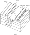
- FIG. 3 is a three-dimensional view of a gallium nitride device used to suppress a "current collapse" effect.
- the P-GaN island structure may include a drain metal D2 and a plurality of P-GaN islands distributed as islands.
- the plurality of P-GaN islands are distributed at intervals in the gate width direction, and the drain metal D2 is continuously distributed in the gate width direction.
- the drain metal D2 grows on the P-GaN islands, to implement local hole injection.
- the drain metal D2 grows on an AlGaN layer. In this way, when the plurality of P-GaN islands are distributed at intervals, a substantial increase in an intrinsic on-resistance of the device can be avoided without causing a substantial loss of chip performance.
- the discontinuous structure of the P-GaN islands needs to be obtained through etching, and design of a spacing distance and etching precisionboth affect a spacing distance between produced P-GaN islands. Therefore, the spacing distance between the P-GaN islands is quite difficult to control.
- An excessively large spacing distance results in a decrease in efficiency of hole injection in the P-GaN island structure and further a decrease in a compensation effect of the electron trap.
- An excessively small spacing distance results in an increase in the intrinsic on-resistance of the device, a decrease in performance of the device, and an increase in use costs of the device.
- Embodiment 1 of this application provides a gallium nitride device, to reduce a risk of an increase in an intrinsic on-resistance of the device while ensuring efficiency of hole injection at P-GaN.
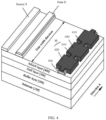
- FIG. 4 is a three-dimensional view of a gallium nitride device according to Embodiment 1 of this application.
- the gallium nitride device includes: a substrate (substrate) 100; a buffer layer (buffer layer) 200 formed over the substrate 100; a gallium nitride GaN layer 300 formed over the buffer layer 200; an aluminum gallium nitride AlGaN layer 400 formed over the gallium nitride GaN layer 300; and a source (source, S), a drain (drain, D), and a gate (gate, G) formed on the AlGaN layer 400.
- the drain includes a P-GaN layer 500 formed on the AlGaN layer 400, and a drain metal M disposed on the P-GaN layer 500 and on the AlGaN layer 400 that is on two sides of the P-GaN layer 500.
- the drain metal M may be an ohmic metal.
- the P-GaN layer 500 is of a strip structure.
- the P-GaN layer 500 has a same width in all positions in a gate width direction.
- the drain metal M may include a plurality of first structural intervals 610 and a plurality of second structural intervals 620 in the gate width direction.
- the plurality of first structural intervals 610 and the plurality of second structural intervals 620 are alternately distributed in the gate width direction.
- the plurality of first structural intervals 610 and the plurality of second structural intervals 620 are an integrated structure in the gate width direction.
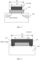
- FIG. 5 is a view of a partial section of a first structural interval 610 in a direction A according to Embodiment 1 of this application. As shown in FIG.
- the drain metal M is formed on the P-GaN layer 500.
- a width H1 of the drain metal M in a direction perpendicular to the gate width direction is less than or equal to a width H2 of the P-GaN layer 500, so that the drain metal M is in contact with only the P-GaN layer 500 but not with the AlGaN layer 400.
- the first structural interval 610 can implement local injection of holes.
- FIG. 6 is a view of a partial section of a second structural interval 620 in a direction A according to Embodiment 1 of this application.
- the drain metal M is formed on the P-GaN layer 500 and on the AlGaN layer 400 that is on the two sides of the P-GaN layer 500.
- a width H3 of the drain metal M in a direction perpendicular to the gate width direction is greater than a width H2 of the P-GaN layer 500.
- the drain metal M has a portion that is located outside a width range of the P-GaN layer 500, forming an extension portion 621.
- a portion of the drain metal located on the P-GaN layer 500 is in contact with the P-GaN layer 500, and the extension portions 621 of the drain metal M are directly formed on the AlGaN layer 400 and form ohmic contact (Ohmic contact) with the AlGaN layer 400.
- the second structural interval 620 can implement current conduction from the drain D to the source S of the device being in an operating state.
- a section of the drain metal M may exhibit a concave structure, which snaps on the P-GaN layer 500.
- the drain metal M encloses the P-GaN layer 500 between the drain metal M and the AlGaN layer 400 by using the concave structure. Portions of the concave structure on two sides are the extension portions 621, and a middle portion of the concave structure is the portion formed on the P-GaN layer 500.
- the gallium nitride device can evenly and alternately form hole injection areas and current conduction areas in the gate width direction, improving consistency in performance of the device at all positions in the gate width direction.
- a quantity of the first structural intervals 610 and a quantity of the second structural intervals 620 may be in a plurality of forms.
- the quantity of the first structural intervals 610 and the quantity of the second structural intervals 620 may be related to a width of the gate.
- a larger width of the gate corresponds to a larger quantity of the first structural intervals 610 and a larger quantity of the second structural intervals 620.
- a smaller width of the gate corresponds to a smaller quantity of the first structural intervals 610 and a smaller quantity of the second structural intervals 620.
- a ratio of a length of the first structural interval 610 to a length of the second structural interval 620 in the gate width direction may be in a plurality of forms.
- a person skilled in the art may determine the ratio based on device performance actually required. For example, to obtain a gallium nitride device with a high concentration of carriers, the length of the first structural interval 610 may be increased; and to improve a gallium nitride device's capability of current conduction from a drain D to a source S, the length of the second structural interval 620 may be increased.
- shapes of the first structural interval 610 and the second structural interval 620 may be in a plurality of forms.
- the first structural interval 610 and the second structural interval 620 may be rectangular, polygonal, circular, oval, or the like.
- the drain metal M is in contact with only the P-GaN layer 500 in the first structural intervals 610, implementing local injection of holes; and the drain metal M forms ohmic contact (Ohmic contact) with the AlGaN layer 400 in the second structural intervals 620, implementing current conduction from the drain D to the source S of the device being in an operating state. Therefore, a risk of an increase in the intrinsic on-resistance of the device can be reduced while ensuring efficiency of hole injection at P-GaN.
- the P-GaN layer 500 does not need to be etched into a discontinuous structure, thereby avoiding an impact of etching precision on performance of the device, and allowing a simpler process.
- Embodiment 2 of this application provides a gallium nitride device production method. The method is used to obtain the gallium nitride device provided in Embodiment 1 of this application or another gallium nitride device.
- FIG. 7A , FIG. 7B , and FIG. 7C are a flowchart of a gallium nitride device production method according to Embodiment 2 of this application. As shown in FIG. 7A , FIG. 7B , and FIG. 7C , the method may include the following steps.
- Step S101 Epitaxially grow a buffer layer 200, a GaN layer 300, and an AlGaN layer 400 sequentially from bottom to top on a substrate 100.
- Step S101 is a conventional step of producing a gallium nitride device and is not further elaborated in this embodiment of this application.
- Step S102 Etch a P-GaN layer 500 of a drain D on the AlGaN layer 400, where the P-GaN layer 500 is of a continuous strip structure in a gate width direction.
- a step of etching a P-GaN layer 600 of a gate G on the AlGaN layer 400 may also be implemented in step S102.
- Etching the P-GaN layer 600 of the gate G on the AlGaN layer 400 is a conventional step of producing a gallium nitride device and is not further elaborated in this embodiment of this application.
- Step S103 Produce a drain metal M on the P-GaN layer 500 and the AlGaN layer 400 that is located on two sides of the P-GaN layer 500.
- the drain metal M includes a plurality of first structural intervals 610 and a plurality of second structural intervals 620 in the gate width direction.
- the first structural intervals 610 and the second structural intervals 620 are continuously and alternately distributed in the gate width direction.
- the drain metal M is etched only on the P-GaN layer 500.
- a width of the drain metal M in a direction perpendicular to the gate width direction is less than or equal to a width of the P-GaN layer 500, so that the drain metal M is in contact with only the P-GaN layer 500 but not with the AlGaN layer 400.
- the drain metal M has a portion that is located outside a width range of the P-GaN layer 500, forming an extension portion 621.
- the extension portions 621 of the drain metal M are directly formed on the AlGaN layer 400 and form ohmic contact (Ohmic contact) with the AlGaN layer 400.
- a step of growing a source metal S-ohm on the AlGaN layer 400 and a step of growing a gate metal G-M on the P-GaN layer 600 of the gate G may also be implemented in step S103.
- Growing the source metal S-ohm on the AlGaN layer 400 and growing the gate metal G-M on the P-GaN layer 600 of the gate G are both conventional steps of producing a gallium nitride device and are not further elaborated in this embodiment of this application.
- Embodiment 3 of this application provides a gallium nitride device, to reduce a risk of an increase in an intrinsic on-resistance of the device while ensuring efficiency of hole injection at P-GaN.
- FIG. 8 is a three-dimensional view of a gallium nitride device according to Embodiment 3 of this application.
- the gallium nitride device includes: a substrate (substrate) 100; a buffer layer 200 formed over the substrate 100; a gallium nitride GaN layer 300 formed over the buffer layer 200; an aluminum gallium nitride AlGaN layer 400 formed over the gallium nitride GaN layer 300; and a source (source, S), a drain (drain, D), and a gate (gate, G) formed on the AlGaN layer 400.
- the drain includes a P-GaN layer 500 formed on the AlGaN layer 400, and a drain metal M disposed on the P-GaN layer 500 and on the AlGaN layer 400 that is on two sides of the P-GaN layer 500.
- the P-GaN layer 500 is of a strip structure.
- the P-GaN layer 500 has a same width in all positions in a gate width direction.
- the drain metal M may include a plurality of first structural intervals 610 and a plurality of second structural intervals 620 in the gate width direction. The first structural intervals 610 and the second structural intervals 620 are alternately distributed in the gate width direction.
- FIG. 9 is a view of a partial section of a first structural interval 610 according to Embodiment 3 of this application.
- the drain metal M is formed on the P-GaN layer 500 and on the AlGaN layer 400 that is on the two sides of the P-GaN layer 500.
- a width H1 of the drain metal M in a direction perpendicular to the gate width direction is greater than a width H2 of the P-GaN layer 500.
- the drain metal M has a portion that is located outside a width range of the P-GaN layer 500, forming an extension portion 621.
- a portion of the drain metal M located on the P-GaN layer 500 is in contact with the P-GaN layer 500.
- passivation layers 410 are retained.
- the extension portions 621 of the drain metal M are formed on the passivation layers 410, and are in contact with only the passivation layers 410 but not with the AlGaN layer 400, isolating the drain metal M from the AlGaN layer 400.
- the first structural interval 610 can implement local injection of holes.
- the P-GaN layer 500 in the first structural interval 610 may further function as a drain field plate. In this case, while implementing local injection of holes, the first structural interval 610 has a capability of balancing a high-voltage electric field at the drain, improving performance of the device.
- FIG. 10 is a view of a partial section of a second structural interval 620 according to Embodiment 3 of this application.
- the drain metal M is formed on the P-GaN layer 500 and on the AlGaN layer 400 that is on the two sides of the P-GaN layer 500.
- a width H1 of the drain metal M in the direction perpendicular to the gate width direction is greater than a width H2 of the P-GaN layer 500.
- the drain metal M has a portion that is located outside a width range of the P-GaN layer 500, forming an extension portion 621.
- a portion of the drain metal M located on the P-GaN layer 500 is in contact with the P-GaN layer 500.
- passivation layers 410 are not retained, that is, the passivation layers 410 are removed by etching.
- the extension portions 621 of the drain metal M are directly formed on the AlGaN layer 400 and form ohmic contact (Ohmic contact) with the AlGaN layer 400.
- the second structural interval 620 can implement current conduction from the drain D to the source S of the device being in an operating state.
- the width of the drain metal M in the first structural interval 610 is the same as the width H1 of the drain metal M in the second structural interval 620, to reduce a difficulty of a process and facilitate production.
- a section of the drain metal M may exhibit a concave structure, which snaps on the P-GaN layer 500.
- the drain metal M encloses the P-GaN layer 500 by using the concave structure.
- Portions of the concave structure on two sides are the extension portions 621, and a middle portion of the concave structure is the portion that is in contact with the P-GaN layer 500.
- the drain metal M is in contact with only the P-GaN layer 500 in the first structural intervals 610, implementing local injection of holes; and the drain metal M forms ohmic contact (Ohmic contact) with the AlGaN layer 400 in the second structural intervals 620, implementing current conduction from the drain D to the source S of the device being in an operating state. Therefore, a risk of an increase in the intrinsic on-resistance of the device can be reduced while ensuring efficiency of hole injection at P-GaN.
- the P-GaN layer 500 does not need to be etched into a discontinuous structure, thereby avoiding an impact of etching precision on performance of the device, and allowing a simpler process.
- the P-GaN layer 500 in the first structural interval 610 may further function as a drain field plate. In this case, while implementing local injection of holes, the first structural interval 610 has a capability of balancing a high-voltage electric field at the drain, improving performance of the device.
- Embodiment 4 of this application provides a gallium nitride device production method. The method is used to obtain the gallium nitride device provided in Embodiment 3 of this application or another gallium nitride device.
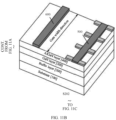
- FIG. 11A , FIG. 11B , and FIG. 11C are a flowchart of a gallium nitride device production method according to Embodiment 4 of this application. As shown in FIG. 11A , FIG. 11B , and FIG. 11C , the method may include the following steps.
- Step S201 Epitaxially grow a buffer layer 200, a GaN layer 300, and an AlGaN layer 400 sequentially from bottom to top on a substrate 100.
- Step S201 is a conventional step of producing a gallium nitride device and is not further elaborated in this embodiment of this application.
- Step S202 Etch a P-GaN layer 500 of a drain D on the AlGaN layer 400, where the P-GaN layer 500 of the drain D may be of a strip structure continuously generated in a gate width direction.
- passivation layers 410 in areas on two sides of the P-GaN layer 500 may be retained at specific intervals in the gate width direction, that is, the passivation layers 410 may be removed by etching at intervals.
- a step of etching a P-GaN layer 600 of a gate G on the AlGaN layer 400 may also be implemented in step S202.
- Etching the P-GaN layer 600 of the gate G on the AlGaN layer 400 is a conventional step of producing a gallium nitride device and is not further elaborated in this embodiment of this application.
- Step S203 Produce a drain metal M on the P-GaN layer 500 and the AlGaN layer 400 that is located on the two sides of the P-GaN layer 500.
- the drain metal M may be continuously distributed in the gate width direction.
- a width of the drain metal M is greater than a width of the P-GaN layer 500.
- the drain metal M on each side of the P-GaN layer 500, the drain metal M has a portion that is located outside a width range of the P-GaN layer 500, forming an extension portion 621. Because the passivation layers 410 in the areas on the two sides of the P-GaN layer 500 are in different etching states, the drain metal M may include a plurality of first structural intervals 610 and a plurality of second structural intervals 620 in the gate width direction. The first structural intervals 610 and the second structural intervals 620 are continuously and alternately distributed in the gate width direction.
- the drain metal M forms the first structural interval 610.
- a portion of the drain metal M located on the P-GaN layer 500 is in contact with the P-GaN layer 500; and the extension portions 621 of the drain metal M are formed on the passivation layers 410, and are in contact with only the passivation layers 410 but not with the AlGaN layer 400.
- the drain metal M forms the second structural interval 620.
- a portion of the drain metal M located on the P-GaN layer 500 is in contact with the P-GaN layer 500; and the extension portions 621 of the drain metal M are directly formed on the AlGaN layer 400 and form ohmic contact (Ohmic contact) with the AlGaN layer 400.
- a step of growing a source metal S-ohm on the AlGaN layer 400 and a step of growing a gate metal G-M on the P-GaN layer 600 of the gate G may also be implemented in step S203.
- Growing the source metal S-ohm on the AlGaN layer 400 and growing the gate metal G-M on the P-GaN layer 600 of the gate G are both conventional steps of producing a gallium nitride device and are not further elaborated in this embodiment of this application.
- Embodiment 5 of this application provides a gallium nitride device.
- FIG. 12 is a three-dimensional view of a structure of the gallium nitride device according to Embodiment 5 of this application.
- a difference between the gallium nitride device provided in Embodiment 5 of this application and the gallium nitride device provided in Embodiment 1 lies in that: first structural intervals 610 and second structural intervals 620 in a drain metal M are alternately distributed rather than continuously distributed in a gate width direction, and there is specific spacing between a first structural interval 610 and a second structural interval 620 that are adjacent.
- An embodiment of this application further provides an electronic device.
- the electronic device may be, for example, a power adapter, a rectifier, an inverter, a frequency converter, a server, a remote radio unit (remote radio unit, RRU), or a switching power supply.
- the electronic device may include one or more gallium nitride devices provided in embodiments of this application.
- An embodiment of this application further provides a drive circuit including a gate driver and the gallium nitride device according to the first aspect and the implementations of the first aspect in the embodiments of this application.
- a gate of the gallium nitride device is coupled to a signal output terminal of the gate driver, and a source and a drain of the gallium nitride device are coupled into a load circuit.
- the gate driver is configured to output a first potential to turn on the gallium nitride device, and output a second potential to turn off the gallium nitride device, where the first potential is higher than a turn-on potential of the gallium nitride device, and the second potential is lower than the turn-on potential of the gallium nitride device.
- the gallium nitride device uses the gate for controlling, and electrical signals of different potentials are input to the gate, to control an on/off state of the gallium nitride device.
- the gallium nitride device When the electrical signal input to the gate is higher than a critical potential, the gallium nitride device is turned on.
- the gallium nitride device When the electrical signal input to the gate is lower than the potential, the gallium nitride device is turned off.
- the critical potential may be referred to as the turn-on potential of the gallium nitride device.
- the first potential output by the gate driver may also be referred to as a high potential. Because the first potential is higher than the turn-on potential, the gallium nitride device may be turned on.
- the second potential output by the gate driver may also be referred to as a low potential. Because the second potential is lower than the turn-on potential, the gallium nitride device may be turned off, thereby implementing state control of the gallium nitride device.
- the gallium nitride device may be used as a switching device in the load circuit, and is controlled to be on and off by the gate driver. Because the gallium nitride device overcomes a "current collapse" effect and has a small intrinsic on-resistance and a small device loss, overall operating efficiency of the load circuit can be improved, a total amount of heat generated by the load circuit can be reduced, and operating stability of the load circuit can be improved. It is easy to understand that a person skilled in the art may obtain other embodiments by combining, splitting, or reassembling embodiments of this application based on the several embodiments provided in this application, and these embodiments do not go beyond the protection scope of this application.
Landscapes
- Junction Field-Effect Transistors (AREA)
- Engineering & Computer Science (AREA)
- Manufacturing & Machinery (AREA)
Claims (4)
- Verfahren zur Herstellung einer Galliumnitrid-Vorrichtung, das zur Herstellung einer Galliumnitrid-Vorrichtung verwendet wird, umfassend ein Substrat (100); eine Pufferschicht (200), die über dem Substrat (100) gebildet ist; eine Galliumnitrid (GaN)-Schicht (300), die über der Pufferschicht (200) gebildet ist; eine AlGaN-Schicht (400), die über der Galliumnitrid (GaN)-Schicht (300) gebildet ist; und eine Source (S), ein Drain (D) und ein Gate (G), die auf der AlGaN-Schicht (400) gebildet sind, wobei das Drain (D) eine P-GaN-Schicht (500) und ein Drain-Metall (M) umfasst, wobei das Verfahren Folgendes umfasst:epitaktisches Wachsen der Pufferschicht (200), der GaN-Schicht (300) und der AlGaN-Schicht (400) nacheinander von unten nach oben auf dem Substrat (100);Ätzen der P-GaN-Schicht (500) auf die AlGaN-Schicht (400), wobei die P-GaN-Schicht (500) in einer Gate-Breitenrichtung eine Streifenstruktur aufweist; undHerstellen des Drain-Metalls (M) auf der P-GaN-Schicht (500) und der AlGaN-Schicht (400), die sich auf zwei Seiten der P-GaN-Schicht (500) befindet, so dass das Drain-Metall (M) eine Vielzahl von ersten Strukturintervallen (610) und eine Vielzahl von zweiten Strukturintervallen (620) aufweist, die abwechselnd in Gate-Breitenrichtung angeordnet sind, wobei in den ersten Strukturintervallen (610) das Drain-Metall (M) in Kontakt mit der P-GaN-Schicht (500), jedoch nicht mit der AlGaN-Schicht, steht und in den zweiten Strukturintervallen (620) das Drain-Metall (M) mit der P-GaN-Schicht (500) in Kontakt steht und einen ohmschen Kontakt mit der AlGaN-Schicht (400) bildet.
- Verfahren nach Anspruch 1, wobei die ersten Strukturintervalle (610) unter Verwendung des folgenden Verfahrens erlangt werden: Ätzen des Drain-Metalls (M) auf die P-GaN-Schicht (500), wobei eine Breite des Drain-Metalls (M) in einer Richtung senkrecht zu der Gate-Breitenrichtung kleiner oder gleich einer Breite der P-GaN-Schicht (500) ist, um die ersten Strukturintervalle (610) zu bilden.
- Verfahren nach Anspruch 1, wobei die zweiten Strukturintervalle (620) unter Verwendung des folgenden Verfahrens erlangt werden: Ätzen des Drain-Metalls (M) auf die P-GaN-Schicht (500) und die AlGaN-Schicht (400), die sich auf den beiden Seiten der P-GaN-Schicht (500) befindet, wobei das Drain-Metall (M) Erweiterungsabschnitte umfasst, die sich auf den beiden Seiten der P-GaN-Schicht (500) befinden, und die Erweiterungsabschnitte einen ohmschen Kontakt mit der AlGaN-Schicht (400) bilden, um die zweiten Strukturintervalle (620) zu bilden.
- Verfahren nach Anspruch 1, wobei die ersten Strukturintervalle (610) und die zweiten Strukturintervalle (620) unter Verwendung des folgenden Verfahrens erlangt werden:Durchführen einer Ätzentfernung in Intervallen in der Gate-Breitenrichtung von Passivierungsschichten, die sich in Bereichen auf den beiden Seiten der P-GaN-Schicht (500) befinden; undÄtzen des Drain-Metalls (M) auf die P-GaN-Schicht (500) und die AlGaN-Schicht (400), die sich auf den beiden Seiten der P-GaN-Schicht (500) befindet, wobei das Drain-Metall (M) Erweiterungsabschnitte umfasst, die sich auf den beiden Seiten der P-GaN-Schicht (500) befinden, wobei in den Bereichen, in denen die Passivierungsschichten nicht durch Ätzen entfernt werden, die Erweiterungsabschnitte durch die Passivierungsschichten von der AlGaN-Schicht (400) isoliert werden, um die ersten Strukturintervalle (610) zu bilden, und in den Bereichen, in denen die Passivierungsschichten durch Ätzen entfernt werden, die Erweiterungsabschnitte in Kontakt mit der AlGaN-Schicht (400) stehen, um die zweiten Strukturintervalle (620) zu bilden.
Applications Claiming Priority (1)
| Application Number | Priority Date | Filing Date | Title |
|---|---|---|---|
| CN202110436275.XA CN113224156B (zh) | 2021-04-22 | 2021-04-22 | 一种氮化镓器件、开关功率管、驱动电路及其制作方法 |
Publications (2)
| Publication Number | Publication Date |
|---|---|
| EP4080582A1 EP4080582A1 (de) | 2022-10-26 |
| EP4080582B1 true EP4080582B1 (de) | 2024-04-24 |
Family
ID=77088632
Family Applications (1)
| Application Number | Title | Priority Date | Filing Date |
|---|---|---|---|
| EP22169177.7A Active EP4080582B1 (de) | 2021-04-22 | 2022-04-21 | Galliumnitridvorrichtung, schaltleistungstransistor, treiberschaltung und verfahren zur herstellung einer galliumnitridvorrichtung |
Country Status (4)
| Country | Link |
|---|---|
| US (1) | US20220344485A1 (de) |
| EP (1) | EP4080582B1 (de) |
| JP (1) | JP7368535B2 (de) |
| CN (1) | CN113224156B (de) |
Families Citing this family (12)
| Publication number | Priority date | Publication date | Assignee | Title |
|---|---|---|---|---|
| CN114400246A (zh) * | 2021-12-13 | 2022-04-26 | 晶通半导体(深圳)有限公司 | 反向导通高迁移率晶体管 |
| WO2023110101A1 (en) * | 2021-12-16 | 2023-06-22 | Huawei Digital Power Technologies Co., Ltd. | Gallium nitride power transistor and method for producing a gan power transistor |
| CN114678415B (zh) * | 2022-03-28 | 2022-12-02 | 江苏晶曌半导体有限公司 | 一种具有阵列浮空岛结构的氮化镓肖特基二极管器件 |
| WO2023197213A1 (zh) * | 2022-04-13 | 2023-10-19 | 华为技术有限公司 | 半导体器件及其工作方法、电子设备 |
| CN114823850B (zh) * | 2022-04-15 | 2023-05-05 | 晶通半导体(深圳)有限公司 | P型混合欧姆接触的氮化镓晶体管 |
| CN115001470B (zh) * | 2022-06-02 | 2023-07-21 | 深圳市泰高技术有限公司 | 射频开关芯片、射频开关及电子设备 |
| CN116247097A (zh) * | 2023-03-06 | 2023-06-09 | 湖南三安半导体有限责任公司 | 高电子迁移率晶体管及其制备方法 |
| CN118448451B (zh) * | 2023-11-23 | 2024-12-13 | 荣耀终端有限公司 | 双向开关器件、电子设备和双向开关器件的制备方法 |
| TW202549549A (zh) * | 2024-01-05 | 2025-12-16 | 日商新唐科技日本股份有限公司 | 半導體裝置及其製造方法 |
| TWI901361B (zh) * | 2024-09-24 | 2025-10-11 | 鴻海精密工業股份有限公司 | 半導體元件 |
| TWI915975B (zh) | 2024-09-24 | 2026-02-21 | 鴻海精密工業股份有限公司 | 半導體元件 |
| CN120448162B (zh) * | 2025-07-14 | 2025-09-05 | 重庆联晶通半导体科技有限公司 | 一种GaN器件电流崩溃抑制方法和系统 |
Family Cites Families (13)
| Publication number | Priority date | Publication date | Assignee | Title |
|---|---|---|---|---|
| JP5292895B2 (ja) * | 2008-03-31 | 2013-09-18 | 日本電気株式会社 | 窒化物半導体トランジスタ |
| JP5618571B2 (ja) * | 2010-03-02 | 2014-11-05 | パナソニック株式会社 | 電界効果トランジスタ |
| JP5790461B2 (ja) * | 2011-12-07 | 2015-10-07 | 富士通株式会社 | 化合物半導体装置及びその製造方法 |
| US9171946B2 (en) * | 2013-03-05 | 2015-10-27 | Seoul Semiconductor Co., Ltd. | Nitride semiconductor device and method of manufacturing the same |
| JP6326638B2 (ja) * | 2013-04-25 | 2018-05-23 | パナソニックIpマネジメント株式会社 | 半導体装置 |
| JPWO2016002180A1 (ja) * | 2014-07-04 | 2017-04-27 | パナソニックIpマネジメント株式会社 | 半導体装置 |
| JP6258148B2 (ja) * | 2014-08-05 | 2018-01-10 | 株式会社東芝 | 半導体装置 |
| US9577048B1 (en) * | 2015-09-24 | 2017-02-21 | Epistar Corporation | Heterostructure field-effect transistor |
| EP3651205A1 (de) * | 2018-11-07 | 2020-05-13 | Infineon Technologies Austria AG | Halbleiterbauelement und verfahren dafür |
| US11049960B2 (en) * | 2019-03-06 | 2021-06-29 | Texas Instruments Incorporated | Gallium nitride (GaN) based transistor with multiple p-GaN blocks |
| CN111900203B (zh) * | 2020-06-30 | 2022-08-16 | 中国电子科技集团公司第五十五研究所 | 一种GaN基高空穴迁移率晶体管及其制备方法 |
| CN111952355B (zh) * | 2020-08-21 | 2021-03-12 | 浙江大学 | 基于多漏指结构的GaN HEMT器件及其制备方法 |
| CN112531020B (zh) * | 2020-10-29 | 2025-10-21 | 湖南三安半导体有限责任公司 | 一种具有复合漏极结构的氮化物功率器件及其制作方法 |
-
2021
- 2021-04-22 CN CN202110436275.XA patent/CN113224156B/zh active Active
-
2022
- 2022-04-21 JP JP2022070166A patent/JP7368535B2/ja active Active
- 2022-04-21 EP EP22169177.7A patent/EP4080582B1/de active Active
- 2022-04-22 US US17/727,221 patent/US20220344485A1/en not_active Abandoned
Also Published As
| Publication number | Publication date |
|---|---|
| CN113224156B (zh) | 2023-02-10 |
| EP4080582A1 (de) | 2022-10-26 |
| JP7368535B2 (ja) | 2023-10-24 |
| JP2022167848A (ja) | 2022-11-04 |
| CN113224156A (zh) | 2021-08-06 |
| US20220344485A1 (en) | 2022-10-27 |
Similar Documents
| Publication | Publication Date | Title |
|---|---|---|
| EP4080582A1 (de) | Galliumnitridvorrichtung, schaltleistungstransistor, treiberschaltung und verfahren zur herstellung einer galliumnitridvorrichtung | |
| US12094962B2 (en) | Enhancement-mode semiconductor device and preparation method therefor | |
| US10026834B2 (en) | Method of manufacturing enhanced device and enhanced device | |
| KR100967779B1 (ko) | 화합물 반도체 장치 및 그것을 이용한 도허티 증폭기 | |
| CN102013437B (zh) | 半导体器件及其制造方法 | |
| EP2852978B1 (de) | Hemt-vorrichtung und verfahren zur herstellung davon | |
| WO2010021099A1 (ja) | 電界効果トランジスタ | |
| JP2012119586A (ja) | 化合物半導体装置及びその製造方法 | |
| US11271109B2 (en) | Silicon metal-oxide-semiconductor field effect transistor (Si MOSFET) with a wide-bandgap III-V compound semiconductor group drain and method for fabricating the same | |
| CN102315262B (zh) | 半导体器件及其制造方法 | |
| KR101672396B1 (ko) | 4원계 질화물 전력반도체소자 및 이의 제조 방법 | |
| CN108598163A (zh) | 一种GaN异质结纵向功率器件 | |
| CN107623032A (zh) | 一种新型的GaN异质结场效应晶体管 | |
| WO2023197213A1 (zh) | 半导体器件及其工作方法、电子设备 | |
| TWI732813B (zh) | 半導體裝置,電子部件,電子設備及用於製造半導體裝置之方法 | |
| CN210897283U (zh) | 一种半导体器件 | |
| US20240154030A1 (en) | Semiconductor structures and manufacturing methods therefor | |
| KR102067597B1 (ko) | 질화물 반도체 소자 및 그 제조 방법 | |
| CN216413092U (zh) | 一种功率晶体管及电子设备 | |
| CN102315261B (zh) | 半导体器件及其制造方法 | |
| CN113707708B (zh) | 结型积累层增强型AlGaN/GaN高电子迁移率晶体管及其制作方法 | |
| KR102125386B1 (ko) | 전력 반도체 소자 및 그 제조방법 | |
| CN112331718B (zh) | 一种半导体器件及其制备方法 | |
| CN201829505U (zh) | 半导体器件 | |
| US20140070278A1 (en) | Active Area Shaping of III-Nitride Devices Utilizing Multiple Dielectric Materials |
Legal Events
| Date | Code | Title | Description |
|---|---|---|---|
| PUAI | Public reference made under article 153(3) epc to a published international application that has entered the european phase |
Free format text: ORIGINAL CODE: 0009012 |
|
| STAA | Information on the status of an ep patent application or granted ep patent |
Free format text: STATUS: REQUEST FOR EXAMINATION WAS MADE |
|
| 17P | Request for examination filed |
Effective date: 20220421 |
|
| AK | Designated contracting states |
Kind code of ref document: A1 Designated state(s): AL AT BE BG CH CY CZ DE DK EE ES FI FR GB GR HR HU IE IS IT LI LT LU LV MC MK MT NL NO PL PT RO RS SE SI SK SM TR |
|
| STAA | Information on the status of an ep patent application or granted ep patent |
Free format text: STATUS: EXAMINATION IS IN PROGRESS |
|
| 17Q | First examination report despatched |
Effective date: 20230511 |
|
| GRAP | Despatch of communication of intention to grant a patent |
Free format text: ORIGINAL CODE: EPIDOSNIGR1 |
|
| STAA | Information on the status of an ep patent application or granted ep patent |
Free format text: STATUS: GRANT OF PATENT IS INTENDED |
|
| RIC1 | Information provided on ipc code assigned before grant |
Ipc: H01L 29/20 20060101ALN20231026BHEP Ipc: H01L 29/06 20060101ALI20231026BHEP Ipc: H01L 29/417 20060101ALI20231026BHEP Ipc: H01L 29/778 20060101AFI20231026BHEP |
|
| RIC1 | Information provided on ipc code assigned before grant |
Ipc: H01L 29/20 20060101ALN20231106BHEP Ipc: H01L 29/06 20060101ALI20231106BHEP Ipc: H01L 29/417 20060101ALI20231106BHEP Ipc: H01L 29/778 20060101AFI20231106BHEP |
|
| INTG | Intention to grant announced |
Effective date: 20231123 |
|
| P01 | Opt-out of the competence of the unified patent court (upc) registered |
Effective date: 20240206 |
|
| GRAS | Grant fee paid |
Free format text: ORIGINAL CODE: EPIDOSNIGR3 |
|
| GRAA | (expected) grant |
Free format text: ORIGINAL CODE: 0009210 |
|
| STAA | Information on the status of an ep patent application or granted ep patent |
Free format text: STATUS: THE PATENT HAS BEEN GRANTED |
|
| AK | Designated contracting states |
Kind code of ref document: B1 Designated state(s): AL AT BE BG CH CY CZ DE DK EE ES FI FR GB GR HR HU IE IS IT LI LT LU LV MC MK MT NL NO PL PT RO RS SE SI SK SM TR |
|
| REG | Reference to a national code |
Ref country code: GB Ref legal event code: FG4D |
|
| REG | Reference to a national code |
Ref country code: CH Ref legal event code: EP |
|
| REG | Reference to a national code |
Ref country code: DE Ref legal event code: R096 Ref document number: 602022003000 Country of ref document: DE |
|
| REG | Reference to a national code |
Ref country code: IE Ref legal event code: FG4D |
|
| REG | Reference to a national code |
Ref country code: LT Ref legal event code: MG9D |
|
| REG | Reference to a national code |
Ref country code: NL Ref legal event code: MP Effective date: 20240424 |
|
| REG | Reference to a national code |
Ref country code: AT Ref legal event code: MK05 Ref document number: 1680588 Country of ref document: AT Kind code of ref document: T Effective date: 20240424 |
|
| PG25 | Lapsed in a contracting state [announced via postgrant information from national office to epo] |
Ref country code: NL Free format text: LAPSE BECAUSE OF FAILURE TO SUBMIT A TRANSLATION OF THE DESCRIPTION OR TO PAY THE FEE WITHIN THE PRESCRIBED TIME-LIMIT Effective date: 20240424 |
|
| PG25 | Lapsed in a contracting state [announced via postgrant information from national office to epo] |
Ref country code: NL Free format text: LAPSE BECAUSE OF FAILURE TO SUBMIT A TRANSLATION OF THE DESCRIPTION OR TO PAY THE FEE WITHIN THE PRESCRIBED TIME-LIMIT Effective date: 20240424 |
|
| PG25 | Lapsed in a contracting state [announced via postgrant information from national office to epo] |
Ref country code: IS Free format text: LAPSE BECAUSE OF FAILURE TO SUBMIT A TRANSLATION OF THE DESCRIPTION OR TO PAY THE FEE WITHIN THE PRESCRIBED TIME-LIMIT Effective date: 20240824 |
|
| PG25 | Lapsed in a contracting state [announced via postgrant information from national office to epo] |
Ref country code: BG Free format text: LAPSE BECAUSE OF FAILURE TO SUBMIT A TRANSLATION OF THE DESCRIPTION OR TO PAY THE FEE WITHIN THE PRESCRIBED TIME-LIMIT Effective date: 20240424 |
|
| PG25 | Lapsed in a contracting state [announced via postgrant information from national office to epo] |
Ref country code: HR Free format text: LAPSE BECAUSE OF FAILURE TO SUBMIT A TRANSLATION OF THE DESCRIPTION OR TO PAY THE FEE WITHIN THE PRESCRIBED TIME-LIMIT Effective date: 20240424 Ref country code: FI Free format text: LAPSE BECAUSE OF FAILURE TO SUBMIT A TRANSLATION OF THE DESCRIPTION OR TO PAY THE FEE WITHIN THE PRESCRIBED TIME-LIMIT Effective date: 20240424 |
|
| PG25 | Lapsed in a contracting state [announced via postgrant information from national office to epo] |
Ref country code: GR Free format text: LAPSE BECAUSE OF FAILURE TO SUBMIT A TRANSLATION OF THE DESCRIPTION OR TO PAY THE FEE WITHIN THE PRESCRIBED TIME-LIMIT Effective date: 20240725 |
|
| PG25 | Lapsed in a contracting state [announced via postgrant information from national office to epo] |
Ref country code: PT Free format text: LAPSE BECAUSE OF FAILURE TO SUBMIT A TRANSLATION OF THE DESCRIPTION OR TO PAY THE FEE WITHIN THE PRESCRIBED TIME-LIMIT Effective date: 20240826 |
|
| PG25 | Lapsed in a contracting state [announced via postgrant information from national office to epo] |
Ref country code: ES Free format text: LAPSE BECAUSE OF FAILURE TO SUBMIT A TRANSLATION OF THE DESCRIPTION OR TO PAY THE FEE WITHIN THE PRESCRIBED TIME-LIMIT Effective date: 20240424 |
|
| PG25 | Lapsed in a contracting state [announced via postgrant information from national office to epo] |
Ref country code: AT Free format text: LAPSE BECAUSE OF FAILURE TO SUBMIT A TRANSLATION OF THE DESCRIPTION OR TO PAY THE FEE WITHIN THE PRESCRIBED TIME-LIMIT Effective date: 20240424 |
|
| PG25 | Lapsed in a contracting state [announced via postgrant information from national office to epo] |
Ref country code: PL Free format text: LAPSE BECAUSE OF FAILURE TO SUBMIT A TRANSLATION OF THE DESCRIPTION OR TO PAY THE FEE WITHIN THE PRESCRIBED TIME-LIMIT Effective date: 20240424 |
|
| PG25 | Lapsed in a contracting state [announced via postgrant information from national office to epo] |
Ref country code: LV Free format text: LAPSE BECAUSE OF FAILURE TO SUBMIT A TRANSLATION OF THE DESCRIPTION OR TO PAY THE FEE WITHIN THE PRESCRIBED TIME-LIMIT Effective date: 20240424 |
|
| PG25 | Lapsed in a contracting state [announced via postgrant information from national office to epo] |
Ref country code: PT Free format text: LAPSE BECAUSE OF FAILURE TO SUBMIT A TRANSLATION OF THE DESCRIPTION OR TO PAY THE FEE WITHIN THE PRESCRIBED TIME-LIMIT Effective date: 20240826 Ref country code: PL Free format text: LAPSE BECAUSE OF FAILURE TO SUBMIT A TRANSLATION OF THE DESCRIPTION OR TO PAY THE FEE WITHIN THE PRESCRIBED TIME-LIMIT Effective date: 20240424 Ref country code: NO Free format text: LAPSE BECAUSE OF FAILURE TO SUBMIT A TRANSLATION OF THE DESCRIPTION OR TO PAY THE FEE WITHIN THE PRESCRIBED TIME-LIMIT Effective date: 20240724 Ref country code: LV Free format text: LAPSE BECAUSE OF FAILURE TO SUBMIT A TRANSLATION OF THE DESCRIPTION OR TO PAY THE FEE WITHIN THE PRESCRIBED TIME-LIMIT Effective date: 20240424 Ref country code: IS Free format text: LAPSE BECAUSE OF FAILURE TO SUBMIT A TRANSLATION OF THE DESCRIPTION OR TO PAY THE FEE WITHIN THE PRESCRIBED TIME-LIMIT Effective date: 20240824 Ref country code: HR Free format text: LAPSE BECAUSE OF FAILURE TO SUBMIT A TRANSLATION OF THE DESCRIPTION OR TO PAY THE FEE WITHIN THE PRESCRIBED TIME-LIMIT Effective date: 20240424 Ref country code: GR Free format text: LAPSE BECAUSE OF FAILURE TO SUBMIT A TRANSLATION OF THE DESCRIPTION OR TO PAY THE FEE WITHIN THE PRESCRIBED TIME-LIMIT Effective date: 20240725 Ref country code: FI Free format text: LAPSE BECAUSE OF FAILURE TO SUBMIT A TRANSLATION OF THE DESCRIPTION OR TO PAY THE FEE WITHIN THE PRESCRIBED TIME-LIMIT Effective date: 20240424 Ref country code: ES Free format text: LAPSE BECAUSE OF FAILURE TO SUBMIT A TRANSLATION OF THE DESCRIPTION OR TO PAY THE FEE WITHIN THE PRESCRIBED TIME-LIMIT Effective date: 20240424 Ref country code: BG Free format text: LAPSE BECAUSE OF FAILURE TO SUBMIT A TRANSLATION OF THE DESCRIPTION OR TO PAY THE FEE WITHIN THE PRESCRIBED TIME-LIMIT Effective date: 20240424 Ref country code: AT Free format text: LAPSE BECAUSE OF FAILURE TO SUBMIT A TRANSLATION OF THE DESCRIPTION OR TO PAY THE FEE WITHIN THE PRESCRIBED TIME-LIMIT Effective date: 20240424 Ref country code: RS Free format text: LAPSE BECAUSE OF FAILURE TO SUBMIT A TRANSLATION OF THE DESCRIPTION OR TO PAY THE FEE WITHIN THE PRESCRIBED TIME-LIMIT Effective date: 20240724 |
|
| REG | Reference to a national code |
Ref country code: DE Ref legal event code: R079 Ref document number: 602022003000 Country of ref document: DE Free format text: PREVIOUS MAIN CLASS: H01L0029778000 Ipc: H10D0030470000 |
|
| PG25 | Lapsed in a contracting state [announced via postgrant information from national office to epo] |
Ref country code: DK Free format text: LAPSE BECAUSE OF FAILURE TO SUBMIT A TRANSLATION OF THE DESCRIPTION OR TO PAY THE FEE WITHIN THE PRESCRIBED TIME-LIMIT Effective date: 20240424 |
|
| PG25 | Lapsed in a contracting state [announced via postgrant information from national office to epo] |
Ref country code: EE Free format text: LAPSE BECAUSE OF FAILURE TO SUBMIT A TRANSLATION OF THE DESCRIPTION OR TO PAY THE FEE WITHIN THE PRESCRIBED TIME-LIMIT Effective date: 20240424 |
|
| PG25 | Lapsed in a contracting state [announced via postgrant information from national office to epo] |
Ref country code: CZ Free format text: LAPSE BECAUSE OF FAILURE TO SUBMIT A TRANSLATION OF THE DESCRIPTION OR TO PAY THE FEE WITHIN THE PRESCRIBED TIME-LIMIT Effective date: 20240424 |
|
| PG25 | Lapsed in a contracting state [announced via postgrant information from national office to epo] |
Ref country code: RO Free format text: LAPSE BECAUSE OF FAILURE TO SUBMIT A TRANSLATION OF THE DESCRIPTION OR TO PAY THE FEE WITHIN THE PRESCRIBED TIME-LIMIT Effective date: 20240424 Ref country code: SK Free format text: LAPSE BECAUSE OF FAILURE TO SUBMIT A TRANSLATION OF THE DESCRIPTION OR TO PAY THE FEE WITHIN THE PRESCRIBED TIME-LIMIT Effective date: 20240424 |
|
| REG | Reference to a national code |
Ref country code: DE Ref legal event code: R097 Ref document number: 602022003000 Country of ref document: DE |
|
| PG25 | Lapsed in a contracting state [announced via postgrant information from national office to epo] |
Ref country code: SM Free format text: LAPSE BECAUSE OF FAILURE TO SUBMIT A TRANSLATION OF THE DESCRIPTION OR TO PAY THE FEE WITHIN THE PRESCRIBED TIME-LIMIT Effective date: 20240424 |
|
| PG25 | Lapsed in a contracting state [announced via postgrant information from national office to epo] |
Ref country code: SM Free format text: LAPSE BECAUSE OF FAILURE TO SUBMIT A TRANSLATION OF THE DESCRIPTION OR TO PAY THE FEE WITHIN THE PRESCRIBED TIME-LIMIT Effective date: 20240424 Ref country code: SK Free format text: LAPSE BECAUSE OF FAILURE TO SUBMIT A TRANSLATION OF THE DESCRIPTION OR TO PAY THE FEE WITHIN THE PRESCRIBED TIME-LIMIT Effective date: 20240424 Ref country code: RO Free format text: LAPSE BECAUSE OF FAILURE TO SUBMIT A TRANSLATION OF THE DESCRIPTION OR TO PAY THE FEE WITHIN THE PRESCRIBED TIME-LIMIT Effective date: 20240424 Ref country code: EE Free format text: LAPSE BECAUSE OF FAILURE TO SUBMIT A TRANSLATION OF THE DESCRIPTION OR TO PAY THE FEE WITHIN THE PRESCRIBED TIME-LIMIT Effective date: 20240424 Ref country code: DK Free format text: LAPSE BECAUSE OF FAILURE TO SUBMIT A TRANSLATION OF THE DESCRIPTION OR TO PAY THE FEE WITHIN THE PRESCRIBED TIME-LIMIT Effective date: 20240424 Ref country code: CZ Free format text: LAPSE BECAUSE OF FAILURE TO SUBMIT A TRANSLATION OF THE DESCRIPTION OR TO PAY THE FEE WITHIN THE PRESCRIBED TIME-LIMIT Effective date: 20240424 |
|
| PLBE | No opposition filed within time limit |
Free format text: ORIGINAL CODE: 0009261 |
|
| STAA | Information on the status of an ep patent application or granted ep patent |
Free format text: STATUS: NO OPPOSITION FILED WITHIN TIME LIMIT |
|
| 26N | No opposition filed |
Effective date: 20250127 |
|
| PG25 | Lapsed in a contracting state [announced via postgrant information from national office to epo] |
Ref country code: SI Free format text: LAPSE BECAUSE OF FAILURE TO SUBMIT A TRANSLATION OF THE DESCRIPTION OR TO PAY THE FEE WITHIN THE PRESCRIBED TIME-LIMIT Effective date: 20240424 |
|
| PGFP | Annual fee paid to national office [announced via postgrant information from national office to epo] |
Ref country code: DE Payment date: 20250305 Year of fee payment: 4 |
|
| PG25 | Lapsed in a contracting state [announced via postgrant information from national office to epo] |
Ref country code: SE Free format text: LAPSE BECAUSE OF FAILURE TO SUBMIT A TRANSLATION OF THE DESCRIPTION OR TO PAY THE FEE WITHIN THE PRESCRIBED TIME-LIMIT Effective date: 20240424 |
|
| REG | Reference to a national code |
Ref country code: CH Ref legal event code: H13 Free format text: ST27 STATUS EVENT CODE: U-0-0-H10-H13 (AS PROVIDED BY THE NATIONAL OFFICE) Effective date: 20251125 |
|
| PG25 | Lapsed in a contracting state [announced via postgrant information from national office to epo] |
Ref country code: LU Free format text: LAPSE BECAUSE OF NON-PAYMENT OF DUE FEES Effective date: 20250421 |
|
| PG25 | Lapsed in a contracting state [announced via postgrant information from national office to epo] |
Ref country code: MC Free format text: LAPSE BECAUSE OF FAILURE TO SUBMIT A TRANSLATION OF THE DESCRIPTION OR TO PAY THE FEE WITHIN THE PRESCRIBED TIME-LIMIT Effective date: 20240424 |
|
| REG | Reference to a national code |
Ref country code: BE Ref legal event code: MM Effective date: 20250430 |
|
| PG25 | Lapsed in a contracting state [announced via postgrant information from national office to epo] |
Ref country code: FR Free format text: LAPSE BECAUSE OF NON-PAYMENT OF DUE FEES Effective date: 20250430 |
|
| PG25 | Lapsed in a contracting state [announced via postgrant information from national office to epo] |
Ref country code: BE Free format text: LAPSE BECAUSE OF NON-PAYMENT OF DUE FEES Effective date: 20250430 |
|
| PG25 | Lapsed in a contracting state [announced via postgrant information from national office to epo] |
Ref country code: CH Free format text: LAPSE BECAUSE OF NON-PAYMENT OF DUE FEES Effective date: 20250430 |
|
| PG25 | Lapsed in a contracting state [announced via postgrant information from national office to epo] |
Ref country code: IT Free format text: LAPSE BECAUSE OF FAILURE TO SUBMIT A TRANSLATION OF THE DESCRIPTION OR TO PAY THE FEE WITHIN THE PRESCRIBED TIME-LIMIT Effective date: 20240424 |
|
| PG25 | Lapsed in a contracting state [announced via postgrant information from national office to epo] |
Ref country code: IE Free format text: LAPSE BECAUSE OF NON-PAYMENT OF DUE FEES Effective date: 20250421 |