EP2852978B1 - Hemt-vorrichtung und verfahren zur herstellung davon - Google Patents
Hemt-vorrichtung und verfahren zur herstellung davon Download PDFInfo
- Publication number
- EP2852978B1 EP2852978B1 EP13793235.6A EP13793235A EP2852978B1 EP 2852978 B1 EP2852978 B1 EP 2852978B1 EP 13793235 A EP13793235 A EP 13793235A EP 2852978 B1 EP2852978 B1 EP 2852978B1
- Authority
- EP
- European Patent Office
- Prior art keywords
- layer
- gate
- drain
- stress inducing
- barrier layer
- Prior art date
- Legal status (The legal status is an assumption and is not a legal conclusion. Google has not performed a legal analysis and makes no representation as to the accuracy of the status listed.)
- Active
Links
Images


Classifications
-
- H—ELECTRICITY
- H10—SEMICONDUCTOR DEVICES; ELECTRIC SOLID-STATE DEVICES NOT OTHERWISE PROVIDED FOR
- H10D—INORGANIC ELECTRIC SEMICONDUCTOR DEVICES
- H10D30/00—Field-effect transistors [FET]
- H10D30/01—Manufacture or treatment
- H10D30/015—Manufacture or treatment of FETs having heterojunction interface channels or heterojunction gate electrodes, e.g. HEMT
-
- H—ELECTRICITY
- H10—SEMICONDUCTOR DEVICES; ELECTRIC SOLID-STATE DEVICES NOT OTHERWISE PROVIDED FOR
- H10D—INORGANIC ELECTRIC SEMICONDUCTOR DEVICES
- H10D30/00—Field-effect transistors [FET]
- H10D30/40—FETs having zero-dimensional [0D], one-dimensional [1D] or two-dimensional [2D] charge carrier gas channels
- H10D30/47—FETs having zero-dimensional [0D], one-dimensional [1D] or two-dimensional [2D] charge carrier gas channels having two-dimensional [2D] charge carrier gas channels, e.g. nanoribbon FETs or high electron mobility transistors [HEMT]
- H10D30/471—High electron mobility transistors [HEMT] or high hole mobility transistors [HHMT]
- H10D30/475—High electron mobility transistors [HEMT] or high hole mobility transistors [HHMT] having wider bandgap layer formed on top of lower bandgap active layer, e.g. undoped barrier HEMTs such as i-AlGaN/GaN HEMTs
-
- H—ELECTRICITY
- H10—SEMICONDUCTOR DEVICES; ELECTRIC SOLID-STATE DEVICES NOT OTHERWISE PROVIDED FOR
- H10D—INORGANIC ELECTRIC SEMICONDUCTOR DEVICES
- H10D62/00—Semiconductor bodies, or regions thereof, of devices having potential barriers
- H10D62/80—Semiconductor bodies, or regions thereof, of devices having potential barriers characterised by the materials
- H10D62/85—Semiconductor bodies, or regions thereof, of devices having potential barriers characterised by the materials being Group III-V materials, e.g. GaAs
- H10D62/8503—Nitride Group III-V materials, e.g. AlN or GaN
-
- H—ELECTRICITY
- H10—SEMICONDUCTOR DEVICES; ELECTRIC SOLID-STATE DEVICES NOT OTHERWISE PROVIDED FOR
- H10D—INORGANIC ELECTRIC SEMICONDUCTOR DEVICES
- H10D64/00—Electrodes of devices having potential barriers
- H10D64/20—Electrodes characterised by their shapes, relative sizes or dispositions
- H10D64/27—Electrodes not carrying the current to be rectified, amplified, oscillated or switched, e.g. gates
- H10D64/311—Gate electrodes for field-effect devices
- H10D64/411—Gate electrodes for field-effect devices for FETs
- H10D64/511—Gate electrodes for field-effect devices for FETs for IGFETs
- H10D64/512—Disposition of the gate electrodes, e.g. buried gates
- H10D64/513—Disposition of the gate electrodes, e.g. buried gates within recesses in the substrate, e.g. trench gates, groove gates or buried gates
-
- H—ELECTRICITY
- H10—SEMICONDUCTOR DEVICES; ELECTRIC SOLID-STATE DEVICES NOT OTHERWISE PROVIDED FOR
- H10P—GENERIC PROCESSES OR APPARATUS FOR THE MANUFACTURE OR TREATMENT OF DEVICES COVERED BY CLASS H10
- H10P50/00—Etching of wafers, substrates or parts of devices
- H10P50/73—Etching of wafers, substrates or parts of devices using masks for insulating materials
Definitions
- This disclosure presents a high electron mobility transistor (HEMT) GaN device with a non-uniform lateral two dimensional electron gas profile and a method of manufacturing the same.
- This disclosure relates to type III - nitride high electron mobility transistor (HEMT) devices and in particular to two dimensional electron gas (2DEG) in the drift region.
- HEMT high electron mobility transistor
- 2DEG two dimensional electron gas
- a high electron mobility transistor is a field effect transistor incorporating a junction between two materials with different band gaps (i.e., a heterojunction).
- Gallium nitride (GaN) HEMTs have attracted attention due to their high-power performance.
- GaN gallium nitride
- type III-nitride HEMT devices used in power applications there is a conflicting design trade-off between the on-state resistance and breakdown voltage (BV). Since the relation between the BV and on resistance is at least quadratic, improvement in the BV for a given drift region length results in a significant improvement in the FOM of the device, defined as BV 2 /Ron.
- type III-nitride HEMT devices have a uniform 2DEG density which results in a peak electric field under or near the gate region.
- the electric field distribution tends to be closer to a triangular shape than to the desired trapezoidal shape which reduces the breakdown voltage per unit drift region length of the device.
- the use of field plate and multistep field plates are some of the techniques that are used to improve the electric field distribution.
- field plates typically result in multiple peaks and suffer from less than an ideal flat field distribution, and may exhibit a saw tooth profile.
- Field plates also add to the gate to drain capacitance. In addition, process complexity and cost typically increase with the number of field plate steps.
- U.S. Patent No. 7,038,253 to Furukawa describes a GaN based device on silicon (Si) technology which uses a uniform 2DEG profile in the drift region. Because of the absence of any field shaping technique in the Furukawa device, the breakdown voltage and dynamic on resistance from drain to source is limited by a localized increase in the electric field under the gate region thus requiring over design of the device which degrades the figure of merit (FOM) that such a device can achieve.
- FOM figure of merit
- US2004144991 discloses a compound semiconductor device that comprises an i-GaN buffer layer 12 formed on an SiC substrate 10; an n-AlGaN electron supplying layer 16 formed on the i-GaN buffer layer 12; an n-GaN cap layer 18 formed on the n-AlGaN electron supplying layer 16; a source electrode 20 and a drain electrode 22 formed on the n-GaN cap layer 18; a gate electrode 26 formed on the n-GaN cap layer 18 between the source electrode 20 and the drain electrode 22; a first protection layer 24 formed on the n-GaN cap layer 18 between the source electrode 20 and the drain electrode 22; and a second protection layer 30 buried in an opening 28 formed in the first protection layer 24 between the gate electrode 26 and the drain electrode 22 down to the n-GaN cap layer 18 and formed of an insulation film different from the first protection layer.
- a high electron mobility field effect transistor having a substrate, a channel layer on the substrate and a barrier layer on the channel layer comprises a stress inducing layer on the barrier layer, the stress inducing layer varying the piezo-electric effect in the barrier layer in a drift region between a gate and a drain, wherein a two dimensional electron gas (2DEG) has a non-uniform lateral distribution in the drift region between the gate and the drain.
- HEMT high electron mobility field effect transistor
- a method of fabricating a high electron mobility field effect transistor comprises forming a channel layer on a substrate, forming a barrier layer on the channel layer, and forming a stress inducing layer on the barrier layer, the stress inducing layer varying the piezo-electric effect in the barrier layer in a drift region between a gate and a drain, wherein a two dimensional electron gas (2DEG) has a non-uniform lateral distribution in the drift region between the gate and the drain.
- 2DEG two dimensional electron gas
- the FET device structure 10 is composed of a stack of III-V layers, such as GaN layer 14 and AlGaN layer 16, grown on a substrate 12 that can be any of the suitable substrates that are commonly used to grow type III-Nitride materials.
- Suitable substrates include but are not limited to silicon (Si), Sapphire, silicon carbide (SiC), and bulk single crystal gallium nitride (GaN).
- the stack of III-V layers may include a buffer layer of GaN or aluminum gallium nitride (AlGaN) grown on the substrate 12. Then a type III layer, such as GaN layer 14, for the channel and carrier travelling layer, is grown on the buffer layer. Then a type V layer, such as AlGaN layer 16, for the barrier layer and the carrier supplying layer, is grown on top of the GaN layer 14.
- AlGaN aluminum gallium nitride
- AlGaN aluminum gallium nitride
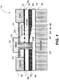
- a stress inducing layer 46 is grown to induce a stress and modulate the charge in the 2DEG 42, as shown in FIG. 1 .
- the stress inducing layer 46 is etched with openings 48 in specific areas, as shown in FIG. 1 , using a mask.
- the stress inducing layer 46 modulates the stress in the stress inducing layer 46.
- the stress varies the piezoelectric effect in the barrier layer 16 and hence the 2DEG 42 in a drift region between the gate 22 and the drain 20.
- the lateral control of the stress in the stress inducing layer 46 over the drift region may be achieved by etching different size openings 48 in the stress inducing layer 46 that either increase or decrease in size from the gate 22 to the drain 20 depending on the polarity of the stress the deposited layer is exerting on the barrier or charge supplying layer.
- the size of the openings 48 are larger near the gate 22 and decrease in size towards the drain 20, as shown in FIG. 1 .
- the size of the openings 48 are made smaller near the gate 22 and increase in size towards the drain 20.
- a non-uniform 2DEG 42 distribution may be achieved by varying the magnitude of piezoelectric effect over the drift region as a function of distance from the gate 22 towards the drain 20 along the drift region.
- the piezoelectric effect in the drift region increases from the gate 22 towards the drain 20, and the size of the openings 48 are larger near the gate 22 and decrease in size towards the drain 20.
- Such an embodiment results in the 2DEG 42 varying in density such that the 2DEG increases in density in the drift region from the gate 22 towards the drain 20.
- the size of the openings 48 may be made smaller near the gate 22 and increased in size towards the drain 20.
- a stress inducing layer 50 is grown on top of the AlGaN layer 16.
- the non-uniform lateral 2DEG 44 is achieved in this embodiment by using Gray scale photolithography to form a stress inducing layer 50 having a lateral profile that has a height that varies.
- Gray scale photolithography uses a gray scale mask to form a stress inducing layer 50 that has a lateral profile and has a height that increases or decreases in the drift region between the gate 22 and the drain 20, depending on the polarity of the stress to be induced.
- the height of the stress inducing layer 50 increases in the drift region between the gate 22 and the drain 20.
- the stress inducing layer 50 varies the magnitude of piezoelectric effect over the drift region as a function of distance from the gate 22 towards the drain 20 along the drift region.
- the stress and the piezoelectric effect in the drift region increases from the gate 22 towards the drain 20.
- Such an embodiment results in the 2DEG 42 varying in density such that the 2DEG 44 increases in density in the drift region from the gate 22 towards the drain 20.
- the height of the stress reducing layer 50 decreases in the drift region in the direction from the gate 22 towards the drain 20.
- the source contact 18 and the drain contact 20 are formed by metal evaporation or metal sputtering to contact the barrier layer 16 after opening a contact window in the stress inducing layer 46, in the embodiment of FIG. 1 , or stress inducing layer 50, in the embodiment of FIG. 2 .
- a passivation layer 24 may be grown on top of the stress inducing layer 46 or the stress inducing layer 50.
- a gate region is then formed by etching a trench through the passivation layer 24 and the stress inducing layer 46 or 50 in a gate area between the source 18 and drain 20 and into the AlGaN layer 16.
- the etched trench may extend through the AlGaN layer 16 and partially into the GaN layer 14 to an appropriate depth.
- a gate dielectric 26 is then deposited over the area between the source 18 and gate 22 and the gate 22 and the drain 20, and also deposited to line the etched trench that extends into the AlGaN layer 16. If the etched trench extends into the GaN layer 14, then the gate dielectric 26 also lines the etched trench that extends into the GaN layer 14.
- gate metal 22 is formed by evaporation or sputtering and fills the etched trench.
- alternating passivation and metallization layers may be formed as a part of back-end processing to improve the parasitic resistance of the device and provide connection to device pads and/or a package.
- Use of the stress inducing layer 46 or 50 to vary the piezo-electric effect in the barrier or charge supplying layer 16, and hence the 2DEG density in the drift region between the gate 22 and the drain 20, may provide a significant improvement of the figure of merit (FOM) in type III Nitride HEMT devices by achieving a flat electric field distribution in the drift region between the gate 22 and the drain 20.
- the 2DEG 42 is varied in the drift region to form a non-uniform lateral 2DEG distribution 44, as shown in FIGs. 1 and 2 .
- a flat electric field distribution results from the non-uniform lateral 2DEG distribution 44 along the drift region which provides the improvement in the figure of merit (FOM), defined as BV 2 /Ron.
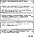
- FIGs. 3A and 3B are flow diagrams for methods of fabricating a HEMT device in accordance with the present disclosure.
- step 100 a channel layer is formed on a substrate. Then in step 102 a barrier layer is formed on the channel layer. Next in step 104 a stress inducing layer is formed on the barrier layer, the stress inducing layer varying the piezo-electric effect in the barrier layer in a drift region between a gate and a drain, wherein a two dimensional electron gas (2deg) has a non-uniform lateral distribution in the drift region between the gate and the drain.
- a two dimensional electron gas (2deg) has a non-uniform lateral distribution in the drift region between the gate and the drain.
- step 106 forming the stress inducing layer on the barrier layer includes forming a material having a plurality of varying size openings between the gate and the drain, the plurality of varying size openings decrease or increase in size from the gate towards the drain.
- forming the stress inducing layer on the barrier layer includes forming a material having a height that increases or decreases from the gate towards the drain using gray scale photolithography.
- a passivation layer is formed over the barrier layer.
- a gate is formed comprising the steps of forming a trench extending through the passivation layer and into the barrier layer, depositing a gate dielectric layer in the trench, and forming gate metal on the gate dielectric.
- the forming a trench extending through the passivation layer and into the barrier layer further includes forming the trench to extend into the channel layer.
- step 116 an opening is formed in the stress inducing layer under the drain for providing contact of the drain to the barrier layer.
- an opening is formed in the stress inducing layer under a source for providing contact of the source to the barrier layer
Landscapes
- Junction Field-Effect Transistors (AREA)
Claims (11)
- Feldeffekttransistor (10) mit hoher Elektronenmobilität mit einem Substrat (12), einer Kanalschicht (14) auf dem Substrat und einer Sperrschicht (16) auf der Kanalschicht (14), wobei der Feldeffekttransistor (10) mit hoher Elektronenmobilität dadurch gekennzeichnet ist, dass er folgendes umfasst:eine stressinduzierende Schicht (46) auf der Sperrschicht (16), wobei die stressinduzierende Schicht (46) ein Material umfasst, das in einem Driftgebiet zwischen einem Gate-Anschluss (22, 26) und einem Drain-Anschluss (20) eine Mehrzahl von Öffnungen (48) mit unterschiedlicher Größe aufweist, so dass die stressinduzierende Schicht (46) den piezoelektrischen Effekt in der Sperrschicht (1 6) entlang des Driftbereichs moduliert;so dass ein zweidimensionales Elektronengas (44) eine ungleichmäßige laterale Verteilung in dem Driftbereich aufweist.
- Feldeffekttransistor (10) mit hoher Elektronenmobilität nach Anspruch 1:wobei die Mehrzahl von Öffnungen (48) mit unterschiedlicher Größe von dem Gate-Anschluss (22, 26) zu dem Drain-Anschluss (20) in der Größe abnimmt; undwobei die Dichte des zweidimensionalen Elektronengases (44) in dem Driftbereich von dem Gate-Anschluss (22, 26) zu dem Drain-Anschluss (20) zunimmt; oderwobei die Mehrzahl von Öffnungen (48) mit unterschiedlicher Größe von dem Gate-Anschluss (22, 26) zu dem Drain-Anschluss (20) in der Größe zunimmt.
- Feldeffekttransistor (10) mit hoher Elektronenmobilität nach Anspruch 1, wobei:das Substrat (12) Silizium, Saphir, Siliziumcarbid oder Volumeneinkristallgalliumnitrid umfasst;die Kanalschicht (14) eine GaN-Schicht umfasst; und die Sperrschicht (16) eine AIGaN-Schicht umfasst.
- Feldeffekttransistor (10) mit hoher Elektronenmobilität nach Anspruch 1, wobei dieser ferner folgendes umfasst:eine Passivierungsschicht (24) über der stressinduzierenden Schicht (46); undwobei der Gate-Anschluss (22, 26) folgendes umfasst:ein Gate-Metall (22), das sich durch die Passivierungsschicht (24) und in die Sperrschicht erstreckt; undeine dielektrische Gate-Schicht (26), welche das Gate-Metall (22) umgibt, das sich durch die Passivierungsschicht (24) und in die Sperrschicht (16) erstreckt.
- Feldeffekttransistor (10) mit hoher Elektronenmobilität nach Anspruch 1, wobei dieser ferner folgendes umfasst:
eine Passivierungsschicht (24) über der stressinduzierenden Schicht (46); und wobei der Gate-Anschluss (22, 26) folgendes umfasst:ein Gate-Metall (22), das sich durch die Passivierungsschicht (24) und die Sperrschicht (16) und in die Kanalschicht (14) erstreckt; undeine dielektrische Gate-Schicht (26), welche das Gate-Metall (22) umgibt, das sich durch die Passivierungsschicht (24), die Sperrschicht (16) und in die Kanalschicht (14) erstreckt. - Feldeffekttransistor (10) mit hoher Elektronenmobilität nach Anspruch 1, wobei dieser ferner folgendes umfasst:eine Öffnung in der stressinduzierenden Schicht (46) unter dem Drain-Anschluss (20), um einen Kontakt des Drain-Anschlusses (20) mit der Sperrschicht (16) bereitzustellen; undeine Öffnung in der stressinduzierenden Schicht (46) unter einem Source-Anschluss (18), um einen Kontakt des Source-Anschlusses (18) mit der Sperrschicht (16) bereitzustellen.
- Verfahren zum Herstellen eines Feldeffekttransistors (10) mit hoher Elektronenmobilität, wobei das Verfahren folgendes umfasst:Ausbilden einer Kanalschicht (14) auf einem Substrat (12); undAusbilden einer Sperrschicht (16) auf der Kanalschicht (14); wobei das Verfahren dadurch gekennzeichnet ist, dass es folgendes umfasst:Ausbilden einer stressinduzierenden Schicht (46) auf der Sperrschicht (16), wobei die stressinduzierende Schicht (46) ein Material umfasst, das in einem Driftgebiet zwischen einem Gate-Anschluss (22, 26) und einem Drain-Anschluss (20) eine Mehrzahl von Öffnungen (48) mit unterschiedlicher Größe aufweist, so dass die stressinduzierende Schicht (46) den piezoelektrischen Effekt in der Sperrschicht (16) entlang des Driftbereichs moduliert;so dass ein zweidimensionales Elektronengas (44) eine ungleichmäßige laterale Verteilung in dem Driftbereich aufweist.
- Verfahren nach Anspruch 7, wobei:wobei die Mehrzahl von Öffnungen (48) mit unterschiedlicher Größe von dem Gate-Anschluss (22, 26) zu dem Drain-Anschluss (20) in der Größe abnimmt; undwobei die Dichte des zweidimensionalen Elektronengases in dem Driftbereich von dem Gate-Anschluss (22, 26) zu dem Drain-Anschluss (20) zunimmt; oderwobei die Mehrzahl von Öffnungen (48) mit unterschiedlicher Größe von dem Gate-Anschluss (22, 26) zu dem Drain-Anschluss (20) in der Größe zunimmt.
- Verfahren nach Anspruch 7, wobei das Verfahren ferner folgendes umfasst:Ausbilden einer Passivierungsschicht (24) über der stressinduzierenden Schicht (46); undAusbilden eines Gate-Anschlusses (22, 26), wobei dies die folgenden Schritte umfasst:Ausbilden eines Grabens, der sich durch die Passivierungsschicht (24) und in die Sperrschicht (16) erstreckt; undAbscheiden einer dielektrischen Gate-Schicht (26) in dem Graben; undAusbilden von Gate-Metall (22) auf der dielektrischen Gate-Schicht (26).
- Verfahren nach Anspruch 9, wobei das Ausbilden eines Grabens, der sich durch die Passivierungsschicht (24) und in die Sperrschicht (16) erstreckt, ferner folgendes umfasst:
Ausbilden des Grabens, so dass sich dieser in die Kanalschicht (14) erstreckt. - Verfahren nach Anspruch 7, wobei dieses ferner folgendes umfasst:Ausbilden einer Öffnung in der stressinduzierenden Schicht (46) unter dem Drain-Anschluss (20), um einen Kontakt des Drain-Anschlusses (20) mit der Sperrschicht (16) bereitzustellen; undAusbilden einer Öffnung in der stressinduzierenden Schicht (46) unter einem Source-Anschluss (18), um einen Kontakt des Source-Anschlusses (18) mit der Sperrschicht (16) bereitzustellen.
Applications Claiming Priority (4)
| Application Number | Priority Date | Filing Date | Title |
|---|---|---|---|
| US13/479,018 US8680536B2 (en) | 2012-05-23 | 2012-05-23 | Non-uniform two dimensional electron gas profile in III-Nitride HEMT devices |
| US13/478,402 US9000484B2 (en) | 2012-05-23 | 2012-05-23 | Non-uniform lateral profile of two-dimensional electron gas charge density in type III nitride HEMT devices using ion implantation through gray scale mask |
| US13/478,609 US9379195B2 (en) | 2012-05-23 | 2012-05-23 | HEMT GaN device with a non-uniform lateral two dimensional electron gas profile and method of manufacturing the same |
| PCT/US2013/040431 WO2013176904A1 (en) | 2012-05-23 | 2013-05-09 | Hemt device and method of manufacturing the same |
Publications (3)
| Publication Number | Publication Date |
|---|---|
| EP2852978A1 EP2852978A1 (de) | 2015-04-01 |
| EP2852978A4 EP2852978A4 (de) | 2016-10-12 |
| EP2852978B1 true EP2852978B1 (de) | 2019-02-27 |
Family
ID=54292265
Family Applications (1)
| Application Number | Title | Priority Date | Filing Date |
|---|---|---|---|
| EP13793235.6A Active EP2852978B1 (de) | 2012-05-23 | 2013-05-09 | Hemt-vorrichtung und verfahren zur herstellung davon |
Country Status (3)
| Country | Link |
|---|---|
| EP (1) | EP2852978B1 (de) |
| CN (1) | CN104412388B (de) |
| WO (1) | WO2013176904A1 (de) |
Families Citing this family (11)
| Publication number | Priority date | Publication date | Assignee | Title |
|---|---|---|---|---|
| CN104377241B (zh) * | 2014-09-30 | 2017-05-03 | 苏州捷芯威半导体有限公司 | 功率半导体器件及其制造方法 |
| CN105609551B (zh) * | 2015-12-28 | 2019-01-29 | 电子科技大学 | 立体多槽栅增强型hemt器件及其制备方法 |
| CN106645323B (zh) * | 2016-11-30 | 2019-01-04 | 南京大学 | 基于氧化物异质结的极性溶剂化学传感器及制备方法 |
| CN116247078A (zh) * | 2018-06-20 | 2023-06-09 | 顶诺微电子(无锡)有限公司 | 一种混合沟道化合物半导体器件 |
| CN109659366A (zh) | 2018-12-21 | 2019-04-19 | 英诺赛科(珠海)科技有限公司 | 高电子迁移率晶体管及其制造方法 |
| CN111384166A (zh) * | 2018-12-29 | 2020-07-07 | 苏州捷芯威半导体有限公司 | 半导体器件和半导体器件制造方法 |
| CN110600536A (zh) * | 2019-09-20 | 2019-12-20 | 中国电子科技集团公司第十三研究所 | 增强型异质结场效应晶体管 |
| CN114447113A (zh) * | 2021-12-20 | 2022-05-06 | 西安电子科技大学 | 基于栅下图形化的新型Fin结构GaN HEMT器件及其制备方法 |
| CN119653809A (zh) * | 2023-09-13 | 2025-03-18 | 中兴通讯股份有限公司 | 高电子迁移率晶体管器件及其制备方法 |
| CN118173558B (zh) * | 2024-02-02 | 2026-01-30 | 西安电子科技大学 | 一种单片集成的全GaN共源共栅场效应晶体管及其制备方法 |
| CN119008625B (zh) * | 2024-08-07 | 2026-03-13 | 西安电子科技大学 | 一种增强型SiC衬底GaN电力电子器件 |
Family Cites Families (8)
| Publication number | Priority date | Publication date | Assignee | Title |
|---|---|---|---|---|
| US20040021152A1 (en) * | 2002-08-05 | 2004-02-05 | Chanh Nguyen | Ga/A1GaN Heterostructure Field Effect Transistor with dielectric recessed gate |
| JP4179539B2 (ja) | 2003-01-15 | 2008-11-12 | 富士通株式会社 | 化合物半導体装置及びその製造方法 |
| JP5093991B2 (ja) * | 2005-03-31 | 2012-12-12 | 住友電工デバイス・イノベーション株式会社 | 半導体装置 |
| US7915643B2 (en) * | 2007-09-17 | 2011-03-29 | Transphorm Inc. | Enhancement mode gallium nitride power devices |
| JP5555985B2 (ja) * | 2008-06-23 | 2014-07-23 | サンケン電気株式会社 | 半導体装置 |
| US20100219452A1 (en) * | 2009-02-27 | 2010-09-02 | Brierley Steven K | GaN HIGH ELECTRON MOBILITY TRANSISTOR (HEMT) STRUCTURES |
| US20120098599A1 (en) * | 2009-06-30 | 2012-04-26 | Univeristy Of Florida Research Foundation Inc. | Enhancement mode hemt for digital and analog applications |
| US8878246B2 (en) * | 2010-06-14 | 2014-11-04 | Samsung Electronics Co., Ltd. | High electron mobility transistors and methods of fabricating the same |
-
2013
- 2013-05-09 EP EP13793235.6A patent/EP2852978B1/de active Active
- 2013-05-09 WO PCT/US2013/040431 patent/WO2013176904A1/en not_active Ceased
- 2013-05-09 CN CN201380025830.3A patent/CN104412388B/zh active Active
Non-Patent Citations (1)
| Title |
|---|
| None * |
Also Published As
| Publication number | Publication date |
|---|---|
| CN104412388A (zh) | 2015-03-11 |
| EP2852978A1 (de) | 2015-04-01 |
| EP2852978A4 (de) | 2016-10-12 |
| WO2013176904A1 (en) | 2013-11-28 |
| CN104412388B (zh) | 2020-03-06 |
Similar Documents
| Publication | Publication Date | Title |
|---|---|---|
| US10192986B1 (en) | HEMT GaN device with a non-uniform lateral two dimensional electron gas profile and method of manufacturing the same | |
| US10700201B2 (en) | HEMT GaN device with a non-uniform lateral two dimensional electron gas profile and method of manufacturing the same | |
| US8933487B2 (en) | Controlling lateral two-dimensional electron hole gas HEMT in type III nitride devices using ion implantation through gray scale mask | |
| JP7368535B2 (ja) | 窒化ガリウムデバイス、スイッチングパワートランジスタ、駆動回路、及び窒化ガリウムデバイス製造方法 | |
| EP2852978A1 (de) | Hemt-vorrichtung und verfahren zur herstellung davon | |
| US10777673B2 (en) | Asymmetrical blocking bidirectional gallium nitride switch | |
| TWI633662B (zh) | 高電子遷移率電晶體及其製造方法 | |
| US8941118B1 (en) | Normally-off III-nitride transistors with high threshold-voltage and low on-resistance | |
| EP3055885B1 (de) | Im normalstand abgeschaltete iii-nitridtransistoren mit hoher schwellenspannung und niedrigem anschaltwiderstand | |
| US9349829B2 (en) | Method of manufacturing a multi-channel HEMT | |
| US9525052B2 (en) | Active area shaping of III-nitride devices utilizing a field plate defined by a dielectric body | |
| JP5609083B2 (ja) | 半導体装置、電子装置、半導体装置の製造方法および使用方法 | |
| JP2016511544A (ja) | 半導体デバイスの電極及びその製造方法 | |
| US11594625B2 (en) | III-N transistor structures with stepped cap layers | |
| US8946778B2 (en) | Active area shaping of III-nitride devices utilizing steps of source-side and drain-side field plates | |
| JP6199147B2 (ja) | 電界効果型化合物半導体装置及びその製造方法 | |
| CN105609550A (zh) | 用于iii族氮化物半导体器件的图案化的背势垒 | |
| US9318592B2 (en) | Active area shaping of III-nitride devices utilizing a source-side field plate and a wider drain-side field plate | |
| US8987784B2 (en) | Active area shaping of III-nitride devices utilizing multiple dielectric materials | |
| CN113394283A (zh) | 具有复合层结构的高压hemt器件 | |
| EP4601010A1 (de) | Verwaltung des elektrischen feldes in einer halbleiterbasierten transistorvorrichtung mit halbleiteroxidinseln | |
| EP2852979A1 (de) | Feldeffekttransistor mit hoher elektronenmobilität und verfahren zur herstellung davon | |
| KR20250063728A (ko) | 고 전자 이동도 트랜지스터 제조 방법 및 고 전자 이동도 트랜지스터 | |
| JP2018037567A (ja) | 半導体装置の製造方法、及び半導体装置 | |
| CN102810563A (zh) | 横向沟槽mesfet |
Legal Events
| Date | Code | Title | Description |
|---|---|---|---|
| PUAI | Public reference made under article 153(3) epc to a published international application that has entered the european phase |
Free format text: ORIGINAL CODE: 0009012 |
|
| 17P | Request for examination filed |
Effective date: 20141218 |
|
| AK | Designated contracting states |
Kind code of ref document: A1 Designated state(s): AL AT BE BG CH CY CZ DE DK EE ES FI FR GB GR HR HU IE IS IT LI LT LU LV MC MK MT NL NO PL PT RO RS SE SI SK SM TR |
|
| AX | Request for extension of the european patent |
Extension state: BA ME |
|
| RIN1 | Information on inventor provided before grant (corrected) |
Inventor name: BOUTROS, KARIM, S. Inventor name: SHINOHARA, KEISUKE Inventor name: KHALIL, SAMEH |
|
| RIN1 | Information on inventor provided before grant (corrected) |
Inventor name: KHALIL, SAMEH Inventor name: BOUTROS, KARIM, S. Inventor name: SHINOHARA, KEISUKE |
|
| DAX | Request for extension of the european patent (deleted) | ||
| RA4 | Supplementary search report drawn up and despatched (corrected) |
Effective date: 20160909 |
|
| RIC1 | Information provided on ipc code assigned before grant |
Ipc: H01L 21/311 20060101ALN20160905BHEP Ipc: H01L 29/778 20060101AFI20160905BHEP Ipc: H01L 21/336 20060101ALI20160905BHEP Ipc: H01L 29/20 20060101ALN20160905BHEP Ipc: H01L 29/423 20060101ALN20160905BHEP |
|
| GRAP | Despatch of communication of intention to grant a patent |
Free format text: ORIGINAL CODE: EPIDOSNIGR1 |
|
| STAA | Information on the status of an ep patent application or granted ep patent |
Free format text: STATUS: GRANT OF PATENT IS INTENDED |
|
| RIC1 | Information provided on ipc code assigned before grant |
Ipc: H01L 21/311 20060101ALN20180906BHEP Ipc: H01L 29/423 20060101ALN20180906BHEP Ipc: H01L 29/20 20060101ALN20180906BHEP Ipc: H01L 29/778 20060101AFI20180906BHEP Ipc: H01L 21/336 20060101ALI20180906BHEP |
|
| RIC1 | Information provided on ipc code assigned before grant |
Ipc: H01L 21/336 20060101ALI20180911BHEP Ipc: H01L 29/20 20060101ALN20180911BHEP Ipc: H01L 29/423 20060101ALN20180911BHEP Ipc: H01L 21/311 20060101ALN20180911BHEP Ipc: H01L 29/778 20060101AFI20180911BHEP |
|
| INTG | Intention to grant announced |
Effective date: 20180927 |
|
| RIN1 | Information on inventor provided before grant (corrected) |
Inventor name: BOUTROS, KARIM, S. Inventor name: KHALIL, SAMEH Inventor name: SHINOHARA, KEISUKE |
|
| GRAS | Grant fee paid |
Free format text: ORIGINAL CODE: EPIDOSNIGR3 |
|
| GRAA | (expected) grant |
Free format text: ORIGINAL CODE: 0009210 |
|
| STAA | Information on the status of an ep patent application or granted ep patent |
Free format text: STATUS: THE PATENT HAS BEEN GRANTED |
|
| AK | Designated contracting states |
Kind code of ref document: B1 Designated state(s): AL AT BE BG CH CY CZ DE DK EE ES FI FR GB GR HR HU IE IS IT LI LT LU LV MC MK MT NL NO PL PT RO RS SE SI SK SM TR |
|
| REG | Reference to a national code |
Ref country code: GB Ref legal event code: FG4D |
|
| REG | Reference to a national code |
Ref country code: CH Ref legal event code: EP |
|
| REG | Reference to a national code |
Ref country code: AT Ref legal event code: REF Ref document number: 1102581 Country of ref document: AT Kind code of ref document: T Effective date: 20190315 |
|
| REG | Reference to a national code |
Ref country code: IE Ref legal event code: FG4D |
|
| REG | Reference to a national code |
Ref country code: DE Ref legal event code: R096 Ref document number: 602013051503 Country of ref document: DE |
|
| REG | Reference to a national code |
Ref country code: NL Ref legal event code: MP Effective date: 20190227 |
|
| REG | Reference to a national code |
Ref country code: LT Ref legal event code: MG4D |
|
| PG25 | Lapsed in a contracting state [announced via postgrant information from national office to epo] |
Ref country code: FI Free format text: LAPSE BECAUSE OF FAILURE TO SUBMIT A TRANSLATION OF THE DESCRIPTION OR TO PAY THE FEE WITHIN THE PRESCRIBED TIME-LIMIT Effective date: 20190227 Ref country code: NO Free format text: LAPSE BECAUSE OF FAILURE TO SUBMIT A TRANSLATION OF THE DESCRIPTION OR TO PAY THE FEE WITHIN THE PRESCRIBED TIME-LIMIT Effective date: 20190527 Ref country code: LT Free format text: LAPSE BECAUSE OF FAILURE TO SUBMIT A TRANSLATION OF THE DESCRIPTION OR TO PAY THE FEE WITHIN THE PRESCRIBED TIME-LIMIT Effective date: 20190227 Ref country code: PT Free format text: LAPSE BECAUSE OF FAILURE TO SUBMIT A TRANSLATION OF THE DESCRIPTION OR TO PAY THE FEE WITHIN THE PRESCRIBED TIME-LIMIT Effective date: 20190627 Ref country code: SE Free format text: LAPSE BECAUSE OF FAILURE TO SUBMIT A TRANSLATION OF THE DESCRIPTION OR TO PAY THE FEE WITHIN THE PRESCRIBED TIME-LIMIT Effective date: 20190227 Ref country code: NL Free format text: LAPSE BECAUSE OF FAILURE TO SUBMIT A TRANSLATION OF THE DESCRIPTION OR TO PAY THE FEE WITHIN THE PRESCRIBED TIME-LIMIT Effective date: 20190227 |
|
| PG25 | Lapsed in a contracting state [announced via postgrant information from national office to epo] |
Ref country code: LV Free format text: LAPSE BECAUSE OF FAILURE TO SUBMIT A TRANSLATION OF THE DESCRIPTION OR TO PAY THE FEE WITHIN THE PRESCRIBED TIME-LIMIT Effective date: 20190227 Ref country code: RS Free format text: LAPSE BECAUSE OF FAILURE TO SUBMIT A TRANSLATION OF THE DESCRIPTION OR TO PAY THE FEE WITHIN THE PRESCRIBED TIME-LIMIT Effective date: 20190227 Ref country code: IS Free format text: LAPSE BECAUSE OF FAILURE TO SUBMIT A TRANSLATION OF THE DESCRIPTION OR TO PAY THE FEE WITHIN THE PRESCRIBED TIME-LIMIT Effective date: 20190627 Ref country code: BG Free format text: LAPSE BECAUSE OF FAILURE TO SUBMIT A TRANSLATION OF THE DESCRIPTION OR TO PAY THE FEE WITHIN THE PRESCRIBED TIME-LIMIT Effective date: 20190527 Ref country code: GR Free format text: LAPSE BECAUSE OF FAILURE TO SUBMIT A TRANSLATION OF THE DESCRIPTION OR TO PAY THE FEE WITHIN THE PRESCRIBED TIME-LIMIT Effective date: 20190528 Ref country code: HR Free format text: LAPSE BECAUSE OF FAILURE TO SUBMIT A TRANSLATION OF THE DESCRIPTION OR TO PAY THE FEE WITHIN THE PRESCRIBED TIME-LIMIT Effective date: 20190227 |
|
| REG | Reference to a national code |
Ref country code: AT Ref legal event code: MK05 Ref document number: 1102581 Country of ref document: AT Kind code of ref document: T Effective date: 20190227 |
|
| PG25 | Lapsed in a contracting state [announced via postgrant information from national office to epo] |
Ref country code: DK Free format text: LAPSE BECAUSE OF FAILURE TO SUBMIT A TRANSLATION OF THE DESCRIPTION OR TO PAY THE FEE WITHIN THE PRESCRIBED TIME-LIMIT Effective date: 20190227 Ref country code: EE Free format text: LAPSE BECAUSE OF FAILURE TO SUBMIT A TRANSLATION OF THE DESCRIPTION OR TO PAY THE FEE WITHIN THE PRESCRIBED TIME-LIMIT Effective date: 20190227 Ref country code: AL Free format text: LAPSE BECAUSE OF FAILURE TO SUBMIT A TRANSLATION OF THE DESCRIPTION OR TO PAY THE FEE WITHIN THE PRESCRIBED TIME-LIMIT Effective date: 20190227 Ref country code: SK Free format text: LAPSE BECAUSE OF FAILURE TO SUBMIT A TRANSLATION OF THE DESCRIPTION OR TO PAY THE FEE WITHIN THE PRESCRIBED TIME-LIMIT Effective date: 20190227 Ref country code: CZ Free format text: LAPSE BECAUSE OF FAILURE TO SUBMIT A TRANSLATION OF THE DESCRIPTION OR TO PAY THE FEE WITHIN THE PRESCRIBED TIME-LIMIT Effective date: 20190227 Ref country code: IT Free format text: LAPSE BECAUSE OF FAILURE TO SUBMIT A TRANSLATION OF THE DESCRIPTION OR TO PAY THE FEE WITHIN THE PRESCRIBED TIME-LIMIT Effective date: 20190227 Ref country code: ES Free format text: LAPSE BECAUSE OF FAILURE TO SUBMIT A TRANSLATION OF THE DESCRIPTION OR TO PAY THE FEE WITHIN THE PRESCRIBED TIME-LIMIT Effective date: 20190227 Ref country code: RO Free format text: LAPSE BECAUSE OF FAILURE TO SUBMIT A TRANSLATION OF THE DESCRIPTION OR TO PAY THE FEE WITHIN THE PRESCRIBED TIME-LIMIT Effective date: 20190227 |
|
| REG | Reference to a national code |
Ref country code: DE Ref legal event code: R097 Ref document number: 602013051503 Country of ref document: DE |
|
| PG25 | Lapsed in a contracting state [announced via postgrant information from national office to epo] |
Ref country code: SM Free format text: LAPSE BECAUSE OF FAILURE TO SUBMIT A TRANSLATION OF THE DESCRIPTION OR TO PAY THE FEE WITHIN THE PRESCRIBED TIME-LIMIT Effective date: 20190227 Ref country code: PL Free format text: LAPSE BECAUSE OF FAILURE TO SUBMIT A TRANSLATION OF THE DESCRIPTION OR TO PAY THE FEE WITHIN THE PRESCRIBED TIME-LIMIT Effective date: 20190227 |
|
| REG | Reference to a national code |
Ref country code: CH Ref legal event code: PL |
|
| PG25 | Lapsed in a contracting state [announced via postgrant information from national office to epo] |
Ref country code: AT Free format text: LAPSE BECAUSE OF FAILURE TO SUBMIT A TRANSLATION OF THE DESCRIPTION OR TO PAY THE FEE WITHIN THE PRESCRIBED TIME-LIMIT Effective date: 20190227 |
|
| PLBE | No opposition filed within time limit |
Free format text: ORIGINAL CODE: 0009261 |
|
| STAA | Information on the status of an ep patent application or granted ep patent |
Free format text: STATUS: NO OPPOSITION FILED WITHIN TIME LIMIT |
|
| GBPC | Gb: european patent ceased through non-payment of renewal fee |
Effective date: 20190527 |
|
| PG25 | Lapsed in a contracting state [announced via postgrant information from national office to epo] |
Ref country code: CH Free format text: LAPSE BECAUSE OF NON-PAYMENT OF DUE FEES Effective date: 20190531 Ref country code: LI Free format text: LAPSE BECAUSE OF NON-PAYMENT OF DUE FEES Effective date: 20190531 Ref country code: MC Free format text: LAPSE BECAUSE OF FAILURE TO SUBMIT A TRANSLATION OF THE DESCRIPTION OR TO PAY THE FEE WITHIN THE PRESCRIBED TIME-LIMIT Effective date: 20190227 |
|
| 26N | No opposition filed |
Effective date: 20191128 |
|
| REG | Reference to a national code |
Ref country code: BE Ref legal event code: MM Effective date: 20190531 |
|
| PG25 | Lapsed in a contracting state [announced via postgrant information from national office to epo] |
Ref country code: LU Free format text: LAPSE BECAUSE OF NON-PAYMENT OF DUE FEES Effective date: 20190509 Ref country code: SI Free format text: LAPSE BECAUSE OF FAILURE TO SUBMIT A TRANSLATION OF THE DESCRIPTION OR TO PAY THE FEE WITHIN THE PRESCRIBED TIME-LIMIT Effective date: 20190227 |
|
| PG25 | Lapsed in a contracting state [announced via postgrant information from national office to epo] |
Ref country code: TR Free format text: LAPSE BECAUSE OF FAILURE TO SUBMIT A TRANSLATION OF THE DESCRIPTION OR TO PAY THE FEE WITHIN THE PRESCRIBED TIME-LIMIT Effective date: 20190227 |
|
| PG25 | Lapsed in a contracting state [announced via postgrant information from national office to epo] |
Ref country code: IE Free format text: LAPSE BECAUSE OF NON-PAYMENT OF DUE FEES Effective date: 20190509 Ref country code: GB Free format text: LAPSE BECAUSE OF NON-PAYMENT OF DUE FEES Effective date: 20190527 |
|
| PG25 | Lapsed in a contracting state [announced via postgrant information from national office to epo] |
Ref country code: BE Free format text: LAPSE BECAUSE OF NON-PAYMENT OF DUE FEES Effective date: 20190531 |
|
| PG25 | Lapsed in a contracting state [announced via postgrant information from national office to epo] |
Ref country code: FR Free format text: LAPSE BECAUSE OF NON-PAYMENT OF DUE FEES Effective date: 20190531 |
|
| PG25 | Lapsed in a contracting state [announced via postgrant information from national office to epo] |
Ref country code: CY Free format text: LAPSE BECAUSE OF FAILURE TO SUBMIT A TRANSLATION OF THE DESCRIPTION OR TO PAY THE FEE WITHIN THE PRESCRIBED TIME-LIMIT Effective date: 20190227 |
|
| PG25 | Lapsed in a contracting state [announced via postgrant information from national office to epo] |
Ref country code: MT Free format text: LAPSE BECAUSE OF FAILURE TO SUBMIT A TRANSLATION OF THE DESCRIPTION OR TO PAY THE FEE WITHIN THE PRESCRIBED TIME-LIMIT Effective date: 20190227 Ref country code: HU Free format text: LAPSE BECAUSE OF FAILURE TO SUBMIT A TRANSLATION OF THE DESCRIPTION OR TO PAY THE FEE WITHIN THE PRESCRIBED TIME-LIMIT; INVALID AB INITIO Effective date: 20130509 |
|
| PG25 | Lapsed in a contracting state [announced via postgrant information from national office to epo] |
Ref country code: MK Free format text: LAPSE BECAUSE OF FAILURE TO SUBMIT A TRANSLATION OF THE DESCRIPTION OR TO PAY THE FEE WITHIN THE PRESCRIBED TIME-LIMIT Effective date: 20190227 |
|
| P01 | Opt-out of the competence of the unified patent court (upc) registered |
Effective date: 20230523 |
|
| REG | Reference to a national code |
Ref country code: DE Ref legal event code: R079 Ref document number: 602013051503 Country of ref document: DE Free format text: PREVIOUS MAIN CLASS: H01L0029778000 Ipc: H10D0030470000 |
|
| PGFP | Annual fee paid to national office [announced via postgrant information from national office to epo] |
Ref country code: DE Payment date: 20250529 Year of fee payment: 13 |