EP4068543A2 - Schnelle überstromerkennung in einem batteriemanagementsystem - Google Patents
Schnelle überstromerkennung in einem batteriemanagementsystem Download PDFInfo
- Publication number
- EP4068543A2 EP4068543A2 EP22161512.3A EP22161512A EP4068543A2 EP 4068543 A2 EP4068543 A2 EP 4068543A2 EP 22161512 A EP22161512 A EP 22161512A EP 4068543 A2 EP4068543 A2 EP 4068543A2
- Authority
- EP
- European Patent Office
- Prior art keywords
- switching device
- occurrence
- pulse sequence
- determining
- fault
- Prior art date
- Legal status (The legal status is an assumption and is not a legal conclusion. Google has not performed a legal analysis and makes no representation as to the accuracy of the status listed.)
- Granted
Links
Images



Classifications
-
- G—PHYSICS
- G01—MEASURING; TESTING
- G01R—MEASURING ELECTRIC VARIABLES; MEASURING MAGNETIC VARIABLES
- G01R31/00—Arrangements for testing electric properties; Arrangements for locating electric faults; Arrangements for electrical testing characterised by what is being tested not provided for elsewhere
- G01R31/36—Arrangements for testing, measuring or monitoring the electrical condition of accumulators or electric batteries, e.g. capacity or state of charge [SoC]
- G01R31/389—Measuring internal impedance, internal conductance or related variables
-
- H—ELECTRICITY
- H02—GENERATION; CONVERSION OR DISTRIBUTION OF ELECTRIC POWER
- H02H—EMERGENCY PROTECTIVE CIRCUIT ARRANGEMENTS
- H02H3/00—Emergency protective circuit arrangements for automatic disconnection directly responsive to an undesired change from normal electric working condition with or without subsequent reconnection ; integrated protection
- H02H3/08—Emergency protective circuit arrangements for automatic disconnection directly responsive to an undesired change from normal electric working condition with or without subsequent reconnection ; integrated protection responsive to excess current
- H02H3/087—Emergency protective circuit arrangements for automatic disconnection directly responsive to an undesired change from normal electric working condition with or without subsequent reconnection ; integrated protection responsive to excess current for DC applications
-
- H—ELECTRICITY
- H03—ELECTRONIC CIRCUITRY
- H03K—PULSE TECHNIQUE
- H03K17/00—Electronic switching or gating, i.e. not by contact-making and –breaking
- H03K17/08—Modifications for protecting switching circuit against overcurrent or overvoltage
- H03K17/082—Modifications for protecting switching circuit against overcurrent or overvoltage by feedback from the output to the control circuit
-
- G—PHYSICS
- G01—MEASURING; TESTING
- G01R—MEASURING ELECTRIC VARIABLES; MEASURING MAGNETIC VARIABLES
- G01R19/00—Arrangements for measuring currents or voltages or for indicating presence or sign thereof
- G01R19/165—Indicating that current or voltage is either above or below a predetermined value or within or outside a predetermined range of values
- G01R19/16533—Indicating that current or voltage is either above or below a predetermined value or within or outside a predetermined range of values characterised by the application
- G01R19/16538—Indicating that current or voltage is either above or below a predetermined value or within or outside a predetermined range of values characterised by the application in AC or DC supplies
- G01R19/16542—Indicating that current or voltage is either above or below a predetermined value or within or outside a predetermined range of values characterised by the application in AC or DC supplies for batteries
-
- G—PHYSICS
- G01—MEASURING; TESTING
- G01R—MEASURING ELECTRIC VARIABLES; MEASURING MAGNETIC VARIABLES
- G01R19/00—Arrangements for measuring currents or voltages or for indicating presence or sign thereof
- G01R19/165—Indicating that current or voltage is either above or below a predetermined value or within or outside a predetermined range of values
- G01R19/16566—Circuits and arrangements for comparing voltage or current with one or several thresholds and for indicating the result not covered by subgroups G01R19/16504, G01R19/16528, G01R19/16533
- G01R19/16571—Circuits and arrangements for comparing voltage or current with one or several thresholds and for indicating the result not covered by subgroups G01R19/16504, G01R19/16528, G01R19/16533 comparing AC or DC current with one threshold, e.g. load current, over-current, surge current or fault current
-
- G—PHYSICS
- G01—MEASURING; TESTING
- G01R—MEASURING ELECTRIC VARIABLES; MEASURING MAGNETIC VARIABLES
- G01R31/00—Arrangements for testing electric properties; Arrangements for locating electric faults; Arrangements for electrical testing characterised by what is being tested not provided for elsewhere
- G01R31/36—Arrangements for testing, measuring or monitoring the electrical condition of accumulators or electric batteries, e.g. capacity or state of charge [SoC]
- G01R31/367—Software therefor, e.g. for battery testing using modelling or look-up tables
-
- G—PHYSICS
- G01—MEASURING; TESTING
- G01R—MEASURING ELECTRIC VARIABLES; MEASURING MAGNETIC VARIABLES
- G01R31/00—Arrangements for testing electric properties; Arrangements for locating electric faults; Arrangements for electrical testing characterised by what is being tested not provided for elsewhere
- G01R31/36—Arrangements for testing, measuring or monitoring the electrical condition of accumulators or electric batteries, e.g. capacity or state of charge [SoC]
- G01R31/382—Arrangements for monitoring battery or accumulator variables, e.g. SoC
- G01R31/3835—Arrangements for monitoring battery or accumulator variables, e.g. SoC involving only voltage measurements
-
- G—PHYSICS
- G01—MEASURING; TESTING
- G01R—MEASURING ELECTRIC VARIABLES; MEASURING MAGNETIC VARIABLES
- G01R31/00—Arrangements for testing electric properties; Arrangements for locating electric faults; Arrangements for electrical testing characterised by what is being tested not provided for elsewhere
- G01R31/36—Arrangements for testing, measuring or monitoring the electrical condition of accumulators or electric batteries, e.g. capacity or state of charge [SoC]
- G01R31/392—Determining battery ageing or deterioration, e.g. state of health
-
- G—PHYSICS
- G01—MEASURING; TESTING
- G01R—MEASURING ELECTRIC VARIABLES; MEASURING MAGNETIC VARIABLES
- G01R31/00—Arrangements for testing electric properties; Arrangements for locating electric faults; Arrangements for electrical testing characterised by what is being tested not provided for elsewhere
- G01R31/36—Arrangements for testing, measuring or monitoring the electrical condition of accumulators or electric batteries, e.g. capacity or state of charge [SoC]
- G01R31/396—Acquisition or processing of data for testing or for monitoring individual cells or groups of cells within a battery
-
- H—ELECTRICITY
- H02—GENERATION; CONVERSION OR DISTRIBUTION OF ELECTRIC POWER
- H02H—EMERGENCY PROTECTIVE CIRCUIT ARRANGEMENTS
- H02H6/00—Emergency protective circuit arrangements responsive to undesired changes from normal non-electric working conditions using simulators of the apparatus being protected, e.g. using thermal images
-
- H—ELECTRICITY
- H02—GENERATION; CONVERSION OR DISTRIBUTION OF ELECTRIC POWER
- H02H—EMERGENCY PROTECTIVE CIRCUIT ARRANGEMENTS
- H02H7/00—Emergency protective circuit arrangements specially adapted for specific types of electric machines or apparatus or for sectionalised protection of cable or line systems, and effecting automatic switching in the event of an undesired change from normal working conditions
- H02H7/008—Emergency protective circuit arrangements specially adapted for specific types of electric machines or apparatus or for sectionalised protection of cable or line systems, and effecting automatic switching in the event of an undesired change from normal working conditions for protective arrangements according to this subclass
-
- H—ELECTRICITY
- H02—GENERATION; CONVERSION OR DISTRIBUTION OF ELECTRIC POWER
- H02H—EMERGENCY PROTECTIVE CIRCUIT ARRANGEMENTS
- H02H7/00—Emergency protective circuit arrangements specially adapted for specific types of electric machines or apparatus or for sectionalised protection of cable or line systems, and effecting automatic switching in the event of an undesired change from normal working conditions
- H02H7/22—Emergency protective circuit arrangements specially adapted for specific types of electric machines or apparatus or for sectionalised protection of cable or line systems, and effecting automatic switching in the event of an undesired change from normal working conditions for distribution gear, e.g. bus-bar systems; for switching devices
- H02H7/222—Emergency protective circuit arrangements specially adapted for specific types of electric machines or apparatus or for sectionalised protection of cable or line systems, and effecting automatic switching in the event of an undesired change from normal working conditions for distribution gear, e.g. bus-bar systems; for switching devices for switches
-
- H—ELECTRICITY
- H02—GENERATION; CONVERSION OR DISTRIBUTION OF ELECTRIC POWER
- H02H—EMERGENCY PROTECTIVE CIRCUIT ARRANGEMENTS
- H02H3/00—Emergency protective circuit arrangements for automatic disconnection directly responsive to an undesired change from normal electric working condition with or without subsequent reconnection ; integrated protection
- H02H3/02—Details
- H02H3/05—Details with means for increasing reliability, e.g. redundancy arrangements
-
- H—ELECTRICITY
- H02—GENERATION; CONVERSION OR DISTRIBUTION OF ELECTRIC POWER
- H02H—EMERGENCY PROTECTIVE CIRCUIT ARRANGEMENTS
- H02H7/00—Emergency protective circuit arrangements specially adapted for specific types of electric machines or apparatus or for sectionalised protection of cable or line systems, and effecting automatic switching in the event of an undesired change from normal working conditions
- H02H7/18—Emergency protective circuit arrangements specially adapted for specific types of electric machines or apparatus or for sectionalised protection of cable or line systems, and effecting automatic switching in the event of an undesired change from normal working conditions for batteries; for accumulators
Definitions
- the present disclosure generally relates to safety techniques and mechanisms for a Battery Management System (BMS), such as overcurrent detection.
- BMS Battery Management System
- a BMS monitors rechargeable batteries to provide relevant data to control systems, such as battery charge level.
- BMSs can have a variety of applications ranging from grid energy storage to electric vehicles to other consumer products like e-bikes, e-scooters, and so forth.
- Rechargeable batteries being electrochemical in nature, may exhibit a variety of undesirable operational characteristics such as outgassing, leakage of electrolyte, or thermal issues such as overheating or exothermically reacting with oxygen.
- One such undesirable condition is an overcurrent condition, where a larger than intended current is sourced or sunk by an individual cell or battery cell stack. Overcurrent can lead to overheating or even thermal runaway.
- a switching mechanism such as a mechanical relay, may be provided to selectively connect and disconnect the battery from its corresponding load (e.g., an electric vehicle (EV) traction motor or related control circuitry) when the battery is malfunctioning.
- a mechanical relay can be expensive, slow, and bulky.
- Embodiments of the present disclosure provide improved overcurrent detection and mitigation systems, methods, and techniques used in a Battery Management System BMS.
- the BMS may be provided in an EV.
- a BMS monitor may detect an overcurrent using two different techniques, providing redundancy and increasing reliability.
- the first technique may detect an overcurrent based on average power over different, overlapping time periods.
- the second technique may detect an overcurrent based on determining a modeled junction temperature of a switching device, such as a semiconductor element, coupling the battery to a load. Both techniques may take into account historical information of the circuit performance, such as past current glitches. If an overcurrent is detected by either technique, the switching device may be quickly disabled, preventing the switching device from failing. Therefore, the overcurrent detection techniques described herein improve the safety and reliability of a BMS while reducing costs.
- the battery monitor may include a converter circuit with an input to receive a voltage, and an oscillator to generate a pulse sequence based on the voltage.
- the battery monitor may also include a digital circuit with a first detector to detect an occurrence or non-occurrence of a first fault event for the switching device based on a determined characteristic of the pulse sequence measured over at least two different time windows and a a second detector to detect an occurrence or non-occurrence of a second fault event for the switching device by determining a modeled junction temperature of the switching device based on the pulsing sequence.
- the method may include detecting an input voltage; generating a pulse sequence based on the input voltage; determining an occurrence or non-occurrence of a first fault event for the switching device based on a determined characteristic of the pulse sequence measured over at least two different time windows; determining an occurrence or non-occurrence of a second fault event for the switching device by determining a modeled junction temperature of the switching device based on the pulsing sequence; and disabling operation of the switching device, in response to determining the occurrence of the first or second fault events.
- the apparatus may include a converter circuit with an input to receive a voltage, and an oscillator to generate a pulse sequence based on the voltage.
- the apparatus may also include a fault detector including a plurality of timing filters and comparators to: determine power dissipated over a plurality of time windows based on the pulse sequence; for each time window of the plurality of time windows, compare the power dissipated for that time window to a respective power threshold for that window; based on the comparing, detecting an overcurrent event; and in response to detecting the overcurrent event, disabling the switching device.
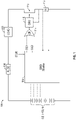
- FIG. 1 illustrates a block diagram of example portions of a BMS 100.
- the BMS 100 may include a plurality of battery cells 102.1-102.N, a BMS monitor 104, a fuse 106, a load 108, a switching device 110, a shunt resistor 112, an OR logic gate 114, and a drive circuit 116.
- the battery cells 102.1-102.N may be provided as a battery module for a battery pack.
- the battery pack may use a Lithium Ion chemistry and provide a stack or other aggregation of battery cells, such as to provide a 48volt nominal output or other desired output. Batteries with different specifications, sizes, and shapes may be used.
- the battery cells 102.1-102.N may be monitored by the BMS monitor 104.
- the BMS monitor 104 may include a plurality of voltage measurement channels, e.g., 16 channels.
- the BMS monitor 104 may be provided as an integrated circuit, which can include a monolithically integrated circuit or an integrated module including multiple integrated circuit die or other circuit elements within a commonly-shared integrated circuit device package, as illustrative examples.
- the BMS monitor 104 may include hardware and software to measure voltage, current, and/or temperature levels of the battery cells 102.1-102.N.
- the BMS monitor 104 may store those measurements values in a memory, such as an EEPROM.
- the BMS monitor 104 may also communicate those measurements to a master controller (not shown) via a communication interface using a wired network, a wireless network, or a combination thereof.
- the battery cells 102.1-102.N may also be coupled to the fuse 106, the load 108, the switching device 110, and the shunt resistor 112.
- the load 108 may be a component receiving power from the battery cells 102.1-102.N, such as an EV traction motor.
- the load 108 may be fully or partially powered by battery cells 102.1-102.N.
- the fuse 106 may be provided for emergency situations where the battery cells 102.1-102.N need to be permanently disconnected from the load 108 (e.g., extreme overheating).
- the switching device 110 may selectively connect and disconnect the battery cells 102.1-102.N to the load 108.
- the switching device 110 may be provided as a metal-oxide-semiconductor field-effect transistor (MOSFET).
- MOSFET metal-oxide-semiconductor field-effect transistor
- the switching device 110 may be provided as a silicon carbide (SiC) MOSFET configured to operate at high voltages.
- SiC silicon carbide
- MOSFETs provide advantages over mechanical relays because of their lower cost and faster response times. However, MOSFETs may have lower fault tolerances such that MOSFETs may be more easily damaged by battery malfunction events, such as overcurrent.
- a MOSFET when used as switching device 110, may be one of the first devices to fail in the circuit. When a MOSFET fails, it often fails as a short.
- This failing-short characteristic may cause catastrophic failure of one or more cells because it creates a short circuit between the battery cells 102.1-102.N and the load 108.
- the fuse 106 may be blown out before significant damage is done, the blown fuse 106 may render the incorporating device (e.g., load) unusable.
- the EV may be rendered undrivable and may have to be taken to a service station and undergo costly repairs.
- the BMS monitor 104 may disable (e.g., turn off, constrain operation) the switching device 110 (e.g., MOSFET) in certain situations, such as overcurrent situations.
- the BMS monitor 104 may detect a voltage across the shunt resistor 112. From the detected voltage, it may detect an overcurrent event and then switch the switching device 110 off in a relatively fast time before the switching device 110 (e.g., MOSFET) can fail.
- the BMS monitor 104 may detect the overcurrent event by using two different techniques (OC1 and OC2), as described in further detail below. If either of the OC detection techniques indicate an overcurrent event, the output of the OR logic gate 114 may trigger the drive circuit 116 to disable the switching device 110.
- the OR logic gate 114 and/or driver circuit 116 may be integrated with the BMS monitor 104.
- overcurrent detection techniques may not be able to accurately detect overcurrent events for the switching device 110.
- Current flow can include transients due to switching in the load 108 (e.g., EV traction motor), thus defining an overcurrent event as simply 'a current exceeding a threshold for a certain period of time' may not be effective in protecting the switching device 110.
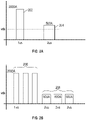
- FIGS. 2A-2B show examples of current spikes in a system.
- FIG. 2A shows two spikes (or glitches): a first spike 202 with a magnitude of 2000A for a duration of 1 microsecond and a second spike 204 with a magnitude of 500A for a duration of 2 microseconds.
- a threshold for detecting an overcurrent event is set for current spikes over 400A for a duration of at least 2 microseconds.
- the second spike 204 500A for a duration of 2 microsecond
- the first spike 202 2000A fora duration of 1 microsecond
- This may be problematic because the first spike 202 may dissipate eight times the energy in a switching device (e.g., MOSFET) as compared to the wider second spike 204.
- a switching device e.g., MOSFET
- FIG. 2B shows a first set of current spikes 206, each with a magnitude of 2000A for a duration of 1 microsecond spike, and second set of current spikes 208, each with a magnitude of 500A for a duration of 2 microseconds.
- a threshold for detecting an overcurrent event is set for current spikes over 600A for a duration of at least 2 microseconds.
- none of the spikes either in the first set or the second set of spikes 206, 208 may trigger detection of an overcurrent event.
- each spike may generate an amount of heat in the switching device (e.g., MOSFET) and the successive nature of the spikes may lead to overheating of the switching device leading to a failure of the switching device.
- overcurrent of a switching device such as a MOSFET, may be based not just on the amount of current at a particular time but also on the history of the circuit performance.
- FIG. 3 illustrates an example portion of a BMS monitor 300.
- the BMS monitor 300 may detect a voltage across a shunt resistor R (e.g., shunt resistor 112 of FIG. 1 ). Based on the detected voltage, the BMS monitor 300 may detect overcurrent events based on two different detection techniques, detecting overcurrent event 1 (OC1) and event 2 (OC2), respectively. As explained above with reference to FIG. 1 , the generation of either overcurrent events (OC1 and/or OC2) may trigger the disabling a switching device, such as a MOSFET (e.g., switching device 110 of FIG. 1 ).
- a switching device such as a MOSFET (e.g., switching device 110 of FIG. 1 ).
- the BMS monitor 300 may include two processing chains 310, 350 corresponding to the two different fault detection techniques.
- the first processing chain 310 may include a first analog front-end circuit 312, a first counter 314, and a first digital engine 316.
- the first analog front-end circuit 312 may receive or detect a voltage across the shunt resistor and convert the detected voltage into a pulse sequence (or periodic pulses).
- the first analog front-end circuit 312 may include a first voltage-to-power converter 312.1 and a first current controlled oscillator (CCO) 312.2.
- the first voltage-to-power converter 312.1 may convert the detected voltage to a power signal.
- the first voltage-to-power converter 312.1 may convert the detected voltage to a current signal, using for example a device having a specified transconductance characteristic.
- the first CCO 312.2 may convert the power signal into the pulse sequence. The pulse sequence therefore may be current-controlled.
- Each pulse may correspond to a "unit of energy.”
- the frequency of the pulse sequence may be proportional to the square of the detected voltage. For example, if the detected voltage of 1 V generates a pulse sequence with a frequency of 1 Hz, then the 2 V detected voltage may generate a pulse sequence with a frequency of 4 Hz (square of 2 V).
- the first counter 314 may count the number of pulses in the generated pulse sequence.
- the first counter 314 may be a rotary counter or other resetting counter such that after it reaches its maximum count it may rollover and begin the count again. For example, if the count is from 1-12, after the count reaches 12, the count begins again 1.
- the first counter 314 may be provided as gray counter, such as a 4-bit gray counter.
- the first counter 314 may be coupled to the first digital engine 316.
- the first digital engine 316 may be implemented using a combination of hardware and software.
- the first digital engine 316 may include a processor, microprocessor, digital state machines, and/or other suitable components.
- the first digital engine 314 may receive the pulse sequence and may detect a first fault event, such as first overcurrent event (OC1), based on the received pulse sequence.
- the pulse sequence generated by the first counter 314 may be generated asynchronously since it represents the current, which can include spikes (or glitches), as discussed above.
- the first digital engine 314 may synchronize the pulse sequence to its system clock (SCLK). For each clock cycle (e.g., 125 nanosecond) or a set of clock cycles of the system clock, the first digital engine 314 may store a previously obtained value of the pulse sequence in register 316.1 and may subtract it from the current obtained value of the pulse sequence using subtractor 316.2 to generate an energy sequence (also referred to as a power sequence) for that clock cycle (or set of clock cycles).
- the energy sequence may correspond to the energy/power dissipated in the last cycle (or set of clock cycles).
- the first counter 314 may be of sufficient size so that it does not complete a full revolution of its count within a clock cycle of the
- the first digital engine 316 may include an OC1 detector 316.3 to detect an overcurrent event based on the generated energy sequence.
- the OC1 detector 316.3 may detect OC1 based on the average of energy across different time periods.
- the OC1 detector 316.3 may use multiple exponential moving average (EMA) windows.
- EMA exponential moving average
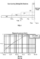
- FIG. 4 illustrates examples of time windows.
- FIG. 4 shows five time windows W1-W5.
- the time windows W1-W5 may be measured based on the present time looking backwards.
- Time window W1 may be shortest window from the present time to a first time backwards, e.g., 1 microsecond.
- Time window W2 may be longer than W1 from the present time to a second time backwards, e.g., 10 microseconds.
- Time window W3 may be longer than W2 from the present time to a third time backwards, e.g., 100 microseconds.
- Time window W4 may be longer than W3 from the current time to a present time backward, e.g., 1000 microseconds.
- Time window W5 may be longer than W4 from the present time to a fifth time backwards, e.g., 10000 microseconds.
- the time windows may be implemented using timing filters.
- the periods of the timing windows may be configurable.
- the periods may be configured based on time periods of a thermal ladder of a MOSFET, as discussed below in further detail.
- an average power dissipated may be determined simultaneously.
- the average power may be a function of the energy sequences observed during the respective time periods.
- the average power for the time windows W1-W5 may show the power dissipated in the last 1 microsecond, 10 microseconds, 100 microseconds, 1000 microseconds, and 10000 microseconds, respectively.
- Each time window may also be associated with a power threshold.
- the average power for each window may be compared to the respective power threshold.
- the individual thresholds for each window may be configurable. For example, the thresholds may be obtained based on simulations of the switching device (MOSFET). The simulations may assume a maximum permissible case temperature and junction temperature, as described in further detail below.
- the BMS monitor 300 may determine the occurrence of the overcurrent event OC1. Using different time windows to determine a digital estimation of power dissipated may eliminate or decrease false positives of overcurrent events coming from current spikes (glitches) while also being responsive to multiple short spikes.
- the second processing chain 350 may include a second analog front-end circuit 352, a first counter 354, and a first digital engine 356.
- the second analog front-end circuit 352 may similar or substantially the same as the first analog front-end circuit 312. As such, the second analog front-end circuit 352 may receive or detect a voltage across the shunt resistor and convert the detected voltage into a pulse sequence (or periodic pulses).
- the second analog front-end circuit 352 may include a second voltage-to-power converter 352.1 and a second current controlled oscillator (CCO) 352.2 and these components may operate the same way as their counterparts in the first analog front-end circuit 312, as described above.
- the second voltage-to-power converter 352.1 may convert the detected voltage to a power signal.
- the second voltage-to-power converter 352.1 may convert the detected voltage to a current signal, using for example a transconductor device.
- the current signal may then be squared to generate the power signal.
- the second CCO 352.2 may convert the power signal into the pulse sequence.
- the pulse sequence therefore may be current-controlled. Each pulse may correspond to a "unit of energy.”
- the frequency of the pulse sequence may be proportional to the square of the detected voltage.
- the second counter 354 may operate in the same way as the first counter 314 described above.
- the second counter 354 may be a rotary counter such that after it reaches its maximum count it may rollover the count and begin again. For example, if the count is from 1-12, after the count reaches 12, the count begins again 1.
- the second counter 354 may be provided as gray counter, such as a 4-bit gray counter.
- one or more analog and counter components in the first and second processing chains 310, 350 may be combined or integrated together.
- a single analog front-end circuit and/or counter may be provided.
- the second counter 354 may be coupled to the second digital engine 356.
- the second digital engine 356 may be implemented using a combination of hardware and software.
- the second digital engine 356 may include a processor, microprocessor, digital state machines, and/or other suitable components.
- the second digital engine 354 may receive the pulse sequence and may detect a second fault event, such as a second overcurrent event (OC2), based on the received pulse sequence.
- a second fault event such as a second overcurrent event (OC2)
- the pulse sequence generated by the second counter 354 may be generated asynchronously since it represents the current, which can include spikes (or glitches), as discussed above.
- SCLK system clock
- the second digital engine 354 may store a previously obtained value of the pulse sequence in register 356.1 and may subtract it from the current obtained value of the pulse sequence using subtractor 356.2 to generate an energy sequence (also referred to as a power sequence) for that clock cycle (or set of clock cycles).
- the energy sequence may correspond to the energy/power dissipated in the last cycle (or set of clock cycles).
- the second counter 354 may be of sufficient size so that it does not complete a full revolution of its count within a clock cycle of the system clock.
- the second digital engine 356 may include an OC2 detector 356.3 to detect an overcurrent event based on the generated energy sequence.
- the OC2 detector 356.3 may determine a modeled (e.g., virtual) junction temperature of the switching device (e.g., MOSFET junction), compare the determined modeled junction temperature to a temperature threshold, and based on the comparison, detect the occurrence of overcurrent event OC2.
- a modeled junction temperature of the switching device e.g., MOSFET junction
- junction temperature of a MOSFET may be a reliable indicator of its safe and proper operability. For example, certain MOSFETS may safely and properly function while their junction temperature is below 175°C and may fail if their junction temperature exceeds 175°C for a period of time. Therefore, an overcurrent condition may be detected based on the junction temperature of the switching MOSFET.
- the actual (or real) junction temperature may be difficult to measure. But the junction temperature is related to the power dissipated by the MOSFET, and not just the instant power dissipated at a select point of time but the historical dissipated power over a period of time. Hence, the OC2 detector 356.3 may determine a modeled junction temperature based on the power dissipated by the MOSFET as detected by the energy sequence and digital representations of the thermal properties of the MOSFET.
- FIG. 5A illustrates a thermal impedance profile of a sample MOSFET
- FIG. 5B shows a circuit representation of a Cauer model of a sample MOSFET
- the x-axis represents a time scale
- the y-axis shows the thermal resistance (or impedance) of the sample MOSFET.
- the thermal resistance may correspond to the temperature difference created between the junction and the case of the MOSFET divided by the amount of energy.
- a MOSFET can be modeled as a network of cascaded resistors and capacitors, known as a Cauer thermal ladder, as shown in FIG. 5B .
- the Cauer model may include a linear network of resistors and capacitors with an input port provided as a current proportional to power and a termination port at the other end provided as a known thermal potential, e.g., case temperature Tcase.
- the junction temperature Tj may be correspond to the node between the first capacitor (Cj1) and first resistor (RTj13) of the Cauer model.
- the values of the resistors and capacitors in the Cauer model are based on the intrinsic properties of the MOSFET, and therefore may be obtained from a digital model of the MOSFET, e.g., SPICE (Simulation Program with Integrated Circuit Emphasis) model.
- the digital representation may be characterized as ⁇ T/(RiCi).
- the OC2 detector 356.3 may obtain the values of the Cauer model of the switching device (e.g., MOSFET), for example from the digital model of the switching device, and may convert them into digital register values. As such, these digital register values for the resistors and capacitors in the Cauer model may be configurable. Thus, based on the energy sequence and the digital Cauer Model register values, the OC2 detector 356.3 may calculate the virtual junction temperature Tj of the switching device. The OC2 detector 353.3 may then compare the virtual junction temperature Tj to a temperature threshold, e.g., 175°C. If the determined virtual junction temperature Tj exceeds the temperature threshold, the BMS monitor 300 (e.g., OC2 detector 356.3) may determine the occurrence of the overcurrent event OC2.
- a temperature threshold e.g. 175°C.
- the switching device may be disabled.
- These detection techniques described herein can quickly detect overcurrent events so that the switching device can be disabled in a relatively fast manner before it fails.
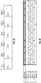
- FIGS. 6A-6F will be used to describe a calculation technique of the modeled (e.g., virtual) junction temperature.
- FIG. 6A shows a sample binary R-C system. Here, two capacitors C1, C2 are coupled in parallel with a resistor R in between, creating a binary R-C system.
- FIG. 6B shows a graph of the current flow in the binary R-C system of FIG. 6A . A first potential V1 is present between C1 and R, and a second potential V2 is present between C2 and R.
- FIG. 6C shows a circuit diagram of a Cauer model of a sample MOSFET.
- the circuit diagram of the model includes a network of resistors (R1, R2, R3, R4, R5, R6) and capacitors (C0, C1, C2, C3, C4, C5). This network of resistors and capacitors may be converted into sets of binary pairs.
- FIG. 6D shows sets of binary R-C pairs.
- Two compute elements may be used to solve the values of the thermal ladder when it is split into binary elements using a switching and timing scheme.
- the first compute element may be dedicated to solving the first RC time constant, and the second compute element may be shared by the other RC elements.
- FIG. 6E shows a network with switched resistors.
- the resistors in the linear network may be replaced by switched resistors and the resistance values may be adjusted accordingly based on their binary position.
- R1 remains R1/1;
- R2 becomes R2/2;
- R3 becomes R3/4;
- R4 becomes R/8;
- R5 becomes R5/16; and
- R6 becomes R6/32 and so on.
- FIG. 6F shows a switch timing scheme. As shown, the switch timing may be set so that the resistor-connection timings are mutually exclusive. That is, only one resistor switch is closed at a time.
- one binary pair may be solved per cycle.
- there may be mutually exclusive time slots for the second compute element such as 2 ⁇ t, 4 ⁇ t, 8 ⁇ t, 16 ⁇ t, 32 ⁇ t, 64 ⁇ t, etc.
- the first compute element may be dedicated to solving the first binary pair.
- the time constant of the first binary pair may be comparable to ⁇ t.
- the second compute element may then be shared by the other binary pairs based on their mutually exclusive time slots.
- the two compute elements may then be able to solve the values of the thermal ladder representing the MOSFET.
- the value of the first capacitor C0 may correspond to the junction temperature with a proportionality constant while the values of the capacitors may correspond to historical data.
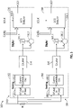
- FIG. 7 illustrates an example portion of a BMS monitor 700.
- the BMS monitor 700 may detect a voltage across a shunt resistor R (e.g., shunt resistor 112 of FIG. 1 ). Based on the detected voltage, the BMS monitor 300 may detect overcurrent events using two different detection techniques, detecting overcurrent event 1 (OC1) and event 2 (OC2), respectively. As explained above with reference to FIG. 1 , the generation of either or both overcurrent events (OC1 and/or OC2) may trigger the disabling a switching device, such as a MOSFET (e.g., switching device 110 of FIG. 1 ).
- a switching device such as a MOSFET (e.g., switching device 110 of FIG. 1 ).
- the BMS monitor 700 may include two processing chains 710, 750 corresponding to the two different overcurrent detection techniques.
- the first processing chain 710 may include analog components: a level shifter 712, a polarity comparator 714, a polarity switch 716, a transconductor 718, a current signal squaring device 720, and a CCO 722.
- the level shifter 712, polarity comparator 714, and polarity switch 716 may detect and adjust the voltage across the shunt resistor.
- the transconductor 718 may convert the detected (and adjusted) voltage to a current signal.
- the transconductor 718 may also apply a gain, which may be adjustable.
- the current signal squaring device 720 may square the current signal to generate a squared current signal, which is representative of a power signal.
- the CCO 722 may convert the squared current signal to a pulse sequence.
- the pulse sequence therefore may be current-controlled. Each pulse may correspond to a "unit of energy.”
- the frequency of the pulse sequence may be proportional to the square of the detected voltage.
- a counter 724 may count the number pulses in the generated pulse sequence.
- the counter 724 may be provided as a rotary counter, such as a gary counter.
- the pulse count may be received by a digital engine.
- SCLK system clock
- the previous value of the pulse count may be subtracted from the current value of the pulse count using a delay 726 and a subtractor 728 to generate an energy sequence (or power sequence) for a given clock cycle (or a set of clock cycles).
- the energy sequence may then be transmitted to a plurality of EMA filters 730.
- the EMA filters 730 may each be defined for a different time period, as discussed above. Each EMA filter 730 may determine the power dissipated in its respective time window.
- Digital comparators 732 may compare the average power from each EMA filter 730 to a respective power threshold.
- the power thresholds for the different windows may be configurable and be set based on register values from a main register file 734.
- the output of the digital comparators 732 may be fed into an OR gate 736. Therefore, if the determined average power for any time window exceeds its respective power threshold, the BMS monitor 700 may detect the occurrence of the overcurrent event OC1.
- the second processing chain 750 may include analog components: a level shifter 752, a polarity comparator 754, a polarity switch 756, a current signal squaring device 760, and a CCO 762. These components may operate in the same or similar manner as their counterparts in the first processing chain 710. One or more of these components in the second processing chain 750 may be combined or integrated together with their counterparts in the first processing chain 710.
- the second processing chain may also include a counter 764, a delay 766, and a subtractor 768 to generate an energy sequence. These components may operate in the same or similar manner as their counterparts in the first processing chain 710. One or more of these components in the second processing chain 750 may be combined or integrated together with their counterparts in the first processing chain 710.
- a Cauer thermal filter 770 may receive the energy sequence. As described herein, the Cauer thermal filter 770 may also receive digital register values of the Cauer model of the switching device, e.g., T CASE , and may calculate a virtual junction temperature Tj of the switching device (e.g., MOSFET). The digital register values may be configurable and may be set based on register values from a redundant register file 772 (or the main register file 734). A digital comparator 774 may compare the virtual junction temperature to a temperature threshold. The temperature threshold may be configurable and may be set based on register values from the redundant register file 772 (or the main register file 734). If the determined virtual junction temperature exceeds the temperature threshold, the BMS Monitor 700 may detect the occurrence of the overcurrent event OC1. In response to the detection of at least one of overcurrent events OC1 and OC2, the switching device may be disabled.
- T CASE digital register values of the Cauer model of the switching device
- Tj virtual junction temperature
- the digital register values may be configurable and may
- Method examples described herein can be machine or computer-implemented at least in part. Some examples can include a computer-readable medium or machine-readable medium encoded with instructions operable to configure an electronic device to perform methods as described in the above examples.
- An implementation of such methods can include code, such as microcode, assembly language code, a higher-level language code, or the like. Such code can include computer readable instructions for performing various methods. The code may form portions of computer program products. Further, in an example, the code can be tangibly stored on one or more volatile, non-transitory, or non-volatile tangible computer-readable media, such as during execution or at other times.
- Examples of these tangible computer-readable media can include, but are not limited to, hard disks, removable magnetic disks, removable optical disks (e.g., compact disks and digital video disks), magnetic cassettes, memory cards or sticks, random access memories (RAMs), read only memories (ROMs), and the like.
Landscapes
- Physics & Mathematics (AREA)
- General Physics & Mathematics (AREA)
- Engineering & Computer Science (AREA)
- Power Engineering (AREA)
- Protection Of Static Devices (AREA)
- Emergency Protection Circuit Devices (AREA)
- Measurement Of Current Or Voltage (AREA)
- Control Of Voltage And Current In General (AREA)
- Charge And Discharge Circuits For Batteries Or The Like (AREA)
Applications Claiming Priority (1)
| Application Number | Priority Date | Filing Date | Title |
|---|---|---|---|
| US17/219,025 US11632105B2 (en) | 2021-03-31 | 2021-03-31 | Fast overcurrent detection in battery management system |
Publications (3)
| Publication Number | Publication Date |
|---|---|
| EP4068543A2 true EP4068543A2 (de) | 2022-10-05 |
| EP4068543A3 EP4068543A3 (de) | 2023-01-04 |
| EP4068543B1 EP4068543B1 (de) | 2026-04-29 |
Family
ID=80735391
Family Applications (1)
| Application Number | Title | Priority Date | Filing Date |
|---|---|---|---|
| EP22161512.3A Active EP4068543B1 (de) | 2021-03-31 | 2022-03-11 | Schnelle überstromerkennung in einem batteriemanagementsystem |
Country Status (4)
| Country | Link |
|---|---|
| US (1) | US11632105B2 (de) |
| EP (1) | EP4068543B1 (de) |
| JP (1) | JP2022158971A (de) |
| CN (1) | CN115144776B (de) |
Families Citing this family (6)
| Publication number | Priority date | Publication date | Assignee | Title |
|---|---|---|---|---|
| US11632105B2 (en) | 2021-03-31 | 2023-04-18 | Analog Devices International Unlimited Company | Fast overcurrent detection in battery management system |
| US12267002B2 (en) | 2021-08-02 | 2025-04-01 | Analog Devices International Unlimited Company | Shunt voltage to digital power sequence conversion with auto-calibrated transconductor, error cancelling reference and current to power converter |
| US20230208169A1 (en) * | 2021-12-29 | 2023-06-29 | Auto Motive Power Inc. | Technique Using a Battery Charger and Battery Management System to Detect Cell Degradation and Pack Imminent Failures |
| CN117075018B (zh) * | 2023-07-20 | 2024-04-16 | 深圳运存科技有限公司 | 一种bms控制板性能测试智能分析管理系统 |
| KR20260028512A (ko) * | 2024-08-22 | 2026-03-04 | 주식회사 엘지에너지솔루션 | 전자 장치, 기록매체 및 그의 배터리 팩의 상태 진단 방법 |
| CN118897180B (zh) * | 2024-08-30 | 2025-07-25 | 重庆云潼科技有限公司 | 一种功率芯片的过电流能力的检测方法、装置及设备 |
Family Cites Families (34)
| Publication number | Priority date | Publication date | Assignee | Title |
|---|---|---|---|---|
| US4038695A (en) | 1976-04-19 | 1977-07-26 | General Electric Company | Static trip unit for circuit protective devices |
| US4782422A (en) | 1987-07-27 | 1988-11-01 | Sundstrand Corporation | I2 t monitoring circuit |
| US5019936A (en) | 1989-03-31 | 1991-05-28 | Square D Company | Voltage-to-frequency squared circuit |
| US5444590A (en) * | 1992-12-04 | 1995-08-22 | Texas Instruments Incorporated | Solid state power controller with power switch protection apparatus |
| US5723915A (en) | 1992-12-04 | 1998-03-03 | Texas Instruments Incorporated | Solid state power controller |
| US5598086A (en) * | 1995-08-03 | 1997-01-28 | Motorola, Inc. | Peak voltage and peak slope detector for a battery charger circuit |
| DE10105982A1 (de) | 2001-02-09 | 2002-10-02 | Siemens Ag | Verfahren zur Auswertung eines Messwertes und zugehörige Schaltungsanordnung |
| US6819011B2 (en) | 2002-11-14 | 2004-11-16 | Fyre Storm, Inc. | Switching power converter controller with watchdog timer |
| US7154232B2 (en) * | 2003-06-24 | 2006-12-26 | International Rectifier Corporation | Ballast control IC with multi-function feedback sense |
| US7126509B2 (en) | 2003-07-17 | 2006-10-24 | Massachusetts Institute Of Technology | Micropower logarithmic analog to digital conversion system and method with offset and temperature compensation |
| US6975103B1 (en) | 2004-06-25 | 2005-12-13 | National Semiconductor Corporation | Resistance ratio digitizing ohmmeter system |
| KR100614654B1 (ko) | 2005-01-04 | 2006-08-22 | 삼성전자주식회사 | 온도와 공정에 따른 출력 변화에 대해 효과적 전력보상을하는 무선 송신기 |
| US8299767B1 (en) | 2006-08-18 | 2012-10-30 | Picor Corporation | Dynamic safe operating area control |
| US7714757B2 (en) | 2007-09-26 | 2010-05-11 | Medtronic, Inc. | Chopper-stabilized analog-to-digital converter |
| JP5323451B2 (ja) * | 2007-11-16 | 2013-10-23 | 古河電気工業株式会社 | 電源供給装置及び電源供給方法 |
| JP5189929B2 (ja) | 2008-08-19 | 2013-04-24 | ルネサスエレクトロニクス株式会社 | 半導体スイッチ制御装置 |
| JP2010279158A (ja) * | 2009-05-28 | 2010-12-09 | Yazaki Corp | 回路保護装置 |
| US9520772B2 (en) | 2010-11-09 | 2016-12-13 | Tdk-Lambda Corporation | Multi-level voltage regulator system |
| WO2013038176A2 (en) | 2011-09-12 | 2013-03-21 | Metroic Limited | Current measurement |
| US20130293139A1 (en) * | 2012-02-24 | 2013-11-07 | Laurence P. Sadwick | Dimmable Driver and Interface |
| US8897727B2 (en) | 2012-06-01 | 2014-11-25 | Qualcomm Incorporated | Power detector with temperature compensation |
| US9634480B1 (en) * | 2013-11-06 | 2017-04-25 | Linear Technology Corporation | MOSFET protection using resistor-capacitor thermal network |
| US9823734B2 (en) * | 2014-08-18 | 2017-11-21 | Atmel Corporation | Instrumenting switch mode power supply to measure circuit power consumption |
| US10374444B2 (en) | 2014-08-26 | 2019-08-06 | Elite Power Innovations, Llc. | Method and system for battery management |
| DE102014218708A1 (de) | 2014-09-17 | 2016-03-17 | Continental Teves Ag & Co. Ohg | Shuntstrommessung mit Temperaturkompensation |
| EP3059857B1 (de) | 2015-02-17 | 2021-11-03 | Nxp B.V. | Zeit-Digital-Wandler und Phasenregelschleife |
| CN104660216B (zh) | 2015-03-02 | 2017-05-10 | 东南大学 | 一种用于Gm‑C滤波器的高精度频率校准电路 |
| US9621043B2 (en) | 2015-08-31 | 2017-04-11 | Dialog Semiconductor (Uk) Limited | Versatile current sensor for switching regulator |
| US10132846B2 (en) | 2016-06-14 | 2018-11-20 | Analog Devices Global | Method of and apparatus for learning the phase error or timing delays within a current transducer and power measurement apparatus including current transducer error correction |
| US10305433B2 (en) | 2017-02-28 | 2019-05-28 | Psemi Corporation | Power amplifier self-heating compensation circuit |
| WO2019145017A1 (en) * | 2018-01-23 | 2019-08-01 | Renesas Electronics Corporation | Over-temperature protection circuit |
| US10976351B2 (en) | 2019-02-12 | 2021-04-13 | Nxp B.V. | Current monitoring device |
| PL3700038T3 (pl) | 2019-02-22 | 2023-01-09 | Future Systems Besitz Gmbh | Urządzenie do przełączania i ochrony obciążenia |
| US11632105B2 (en) | 2021-03-31 | 2023-04-18 | Analog Devices International Unlimited Company | Fast overcurrent detection in battery management system |
-
2021
- 2021-03-31 US US17/219,025 patent/US11632105B2/en active Active
-
2022
- 2022-02-28 CN CN202210183307.4A patent/CN115144776B/zh active Active
- 2022-03-04 JP JP2022033473A patent/JP2022158971A/ja active Pending
- 2022-03-11 EP EP22161512.3A patent/EP4068543B1/de active Active
Also Published As
| Publication number | Publication date |
|---|---|
| US20220321114A1 (en) | 2022-10-06 |
| CN115144776B (zh) | 2026-02-24 |
| CN115144776A (zh) | 2022-10-04 |
| EP4068543A3 (de) | 2023-01-04 |
| US11632105B2 (en) | 2023-04-18 |
| JP2022158971A (ja) | 2022-10-17 |
| EP4068543B1 (de) | 2026-04-29 |
Similar Documents
| Publication | Publication Date | Title |
|---|---|---|
| EP4068543A2 (de) | Schnelle überstromerkennung in einem batteriemanagementsystem | |
| KR102949540B1 (ko) | 배터리 관리 시스템, 배터리 팩, 전기 차량 및 배터리 관리 방법 | |
| US12146905B2 (en) | Insulation resistor detection circuit, method, and apparatus, and storage medium thereof | |
| EP3929606B1 (de) | Batterieverwaltungssystem, batteriepack, elektrofahrzeug und batterieverwaltungsverfahren | |
| EP3428669B1 (de) | Vorrichtung und verfahren zur erkennung des gesundheitszustands einer batterie | |
| US10802078B2 (en) | Current monitoring circuit and coulomb counter circuit | |
| TWI627812B (zh) | 電壓補償主動電池平衡的裝置、系統及方法 | |
| Wei et al. | Model-based fault diagnosis of Lithium-ion battery using strong tracking Extended Kalman Filter | |
| EP3913388B1 (de) | Detektionsverfahren für isolationsprüfschaltung und batterieverwaltungssystem | |
| EP1930737B1 (de) | Detektionsvorrichtung für den isolationswiderstand | |
| KR102701517B1 (ko) | 배터리 관리 장치, 배터리 팩, 에너지 저장 시스템 및 배터리 관리 방법 | |
| EP2848952A1 (de) | Vorrichtung zur einschätzung des ladezustands einer batterie | |
| EP4166963B1 (de) | Batteriediagnosevorrichtung, batteriepack, batteriesystem und batteriediagnoseverfahren | |
| US10852332B2 (en) | Isolation monitoring device and method | |
| US20110049977A1 (en) | Safety and performance optimized controls for large scale electric vehicle battery systems | |
| WO2017114195A1 (zh) | 一种动力电池的内短路检测方法及装置 | |
| EP3133714A1 (de) | Batterieüberwachungsverfahren und -vorrichtung | |
| EP3185348B1 (de) | Ein batterieinformationserkennungs- und kontrollmethode, intelligente batterie, endgerät und computerspeichermedium | |
| US20160149272A1 (en) | Remaining battery life prediction device and battery pack | |
| EP4235196B1 (de) | Schaltererkennungsschaltung, verfahren und schalterdetektor | |
| US9859739B2 (en) | Load driver circuit including load model parameter estimation | |
| EP4481413A1 (de) | Interne kurzschlusserkennung in echtzeit einer batterie | |
| US20210391740A1 (en) | Methods and apparatus for a battery system | |
| EP3754352A1 (de) | Verfahren und system zur verbesserung von batteriekapazitätsschätzungen | |
| Wey et al. | Emi prevention of can-bus-based communication in battery management systems |
Legal Events
| Date | Code | Title | Description |
|---|---|---|---|
| PUAI | Public reference made under article 153(3) epc to a published international application that has entered the european phase |
Free format text: ORIGINAL CODE: 0009012 |
|
| STAA | Information on the status of an ep patent application or granted ep patent |
Free format text: STATUS: THE APPLICATION HAS BEEN PUBLISHED |
|
| AK | Designated contracting states |
Kind code of ref document: A2 Designated state(s): AL AT BE BG CH CY CZ DE DK EE ES FI FR GB GR HR HU IE IS IT LI LT LU LV MC MK MT NL NO PL PT RO RS SE SI SK SM TR |
|
| PUAL | Search report despatched |
Free format text: ORIGINAL CODE: 0009013 |
|
| AK | Designated contracting states |
Kind code of ref document: A3 Designated state(s): AL AT BE BG CH CY CZ DE DK EE ES FI FR GB GR HR HU IE IS IT LI LT LU LV MC MK MT NL NO PL PT RO RS SE SI SK SM TR |
|
| RIC1 | Information provided on ipc code assigned before grant |
Ipc: H03K 17/082 20060101ALI20221129BHEP Ipc: G01R 19/255 20060101ALI20221129BHEP Ipc: G01R 19/252 20060101ALI20221129BHEP Ipc: H02H 7/22 20060101ALI20221129BHEP Ipc: H02H 7/00 20060101ALI20221129BHEP Ipc: H02H 6/00 20060101ALI20221129BHEP Ipc: H02H 3/087 20060101AFI20221129BHEP |
|
| STAA | Information on the status of an ep patent application or granted ep patent |
Free format text: STATUS: REQUEST FOR EXAMINATION WAS MADE |
|
| 17P | Request for examination filed |
Effective date: 20230629 |
|
| RBV | Designated contracting states (corrected) |
Designated state(s): AL AT BE BG CH CY CZ DE DK EE ES FI FR GB GR HR HU IE IS IT LI LT LU LV MC MK MT NL NO PL PT RO RS SE SI SK SM TR |
|
| STAA | Information on the status of an ep patent application or granted ep patent |
Free format text: STATUS: EXAMINATION IS IN PROGRESS |
|
| 17Q | First examination report despatched |
Effective date: 20250520 |
|
| GRAP | Despatch of communication of intention to grant a patent |
Free format text: ORIGINAL CODE: EPIDOSNIGR1 |
|
| STAA | Information on the status of an ep patent application or granted ep patent |
Free format text: STATUS: GRANT OF PATENT IS INTENDED |
|
| RIC1 | Information provided on ipc code assigned before grant |
Ipc: H02H 3/087 20060101AFI20251104BHEP Ipc: H02H 6/00 20060101ALI20251104BHEP Ipc: H02H 7/18 20060101ALI20251104BHEP Ipc: H02H 7/22 20060101ALI20251104BHEP Ipc: H02H 3/05 20060101ALN20251104BHEP |
|
| RIC1 | Information provided on ipc code assigned before grant |
Ipc: H02H 3/087 20060101AFI20251110BHEP Ipc: H02H 6/00 20060101ALI20251110BHEP Ipc: H02H 7/18 20060101ALI20251110BHEP Ipc: H02H 7/22 20060101ALI20251110BHEP Ipc: H02H 3/05 20060101ALN20251110BHEP |
|
| INTG | Intention to grant announced |
Effective date: 20251125 |
|
| GRAS | Grant fee paid |
Free format text: ORIGINAL CODE: EPIDOSNIGR3 |
|
| GRAA | (expected) grant |
Free format text: ORIGINAL CODE: 0009210 |
|
| STAA | Information on the status of an ep patent application or granted ep patent |
Free format text: STATUS: THE PATENT HAS BEEN GRANTED |
|
| AK | Designated contracting states |
Kind code of ref document: B1 Designated state(s): AL AT BE BG CH CY CZ DE DK EE ES FI FR GB GR HR HU IE IS IT LI LT LU LV MC MK MT NL NO PL PT RO RS SE SI SK SM TR |
|
| REG | Reference to a national code |
Ref country code: CH Ref legal event code: F10 Free format text: ST27 STATUS EVENT CODE: U-0-0-F10-F00 (AS PROVIDED BY THE NATIONAL OFFICE) Effective date: 20260429 |