EP3059857B1 - Zeit-Digital-Wandler und Phasenregelschleife - Google Patents
Zeit-Digital-Wandler und Phasenregelschleife Download PDFInfo
- Publication number
- EP3059857B1 EP3059857B1 EP15155327.8A EP15155327A EP3059857B1 EP 3059857 B1 EP3059857 B1 EP 3059857B1 EP 15155327 A EP15155327 A EP 15155327A EP 3059857 B1 EP3059857 B1 EP 3059857B1
- Authority
- EP
- European Patent Office
- Prior art keywords
- output
- integrator
- digital
- input
- time
- Prior art date
- Legal status (The legal status is an assumption and is not a legal conclusion. Google has not performed a legal analysis and makes no representation as to the accuracy of the status listed.)
- Active
Links
- 239000003990 capacitor Substances 0.000 claims description 63
- 230000004044 response Effects 0.000 claims description 10
- 230000003247 decreasing effect Effects 0.000 claims description 2
- 230000000717 retained effect Effects 0.000 claims 1
- 238000006243 chemical reaction Methods 0.000 description 15
- 230000000694 effects Effects 0.000 description 7
- 238000010586 diagram Methods 0.000 description 5
- 238000010606 normalization Methods 0.000 description 3
- 238000007493 shaping process Methods 0.000 description 3
- HIHOWBSBBDRPDW-PTHRTHQKSA-N [(3s,8s,9s,10r,13r,14s,17r)-10,13-dimethyl-17-[(2r)-6-methylheptan-2-yl]-2,3,4,7,8,9,11,12,14,15,16,17-dodecahydro-1h-cyclopenta[a]phenanthren-3-yl] n-[2-(dimethylamino)ethyl]carbamate Chemical compound C1C=C2C[C@@H](OC(=O)NCCN(C)C)CC[C@]2(C)[C@@H]2[C@@H]1[C@@H]1CC[C@H]([C@H](C)CCCC(C)C)[C@@]1(C)CC2 HIHOWBSBBDRPDW-PTHRTHQKSA-N 0.000 description 2
- 238000001914 filtration Methods 0.000 description 2
- 238000000034 method Methods 0.000 description 2
- 239000000872 buffer Substances 0.000 description 1
- 230000009977 dual effect Effects 0.000 description 1
- 238000002513 implantation Methods 0.000 description 1
- 238000013139 quantization Methods 0.000 description 1
- 230000000630 rising effect Effects 0.000 description 1
- 238000005070 sampling Methods 0.000 description 1
- 238000004088 simulation Methods 0.000 description 1
- 230000001960 triggered effect Effects 0.000 description 1
Images


Classifications
-
- H—ELECTRICITY
- H03—ELECTRONIC CIRCUITRY
- H03L—AUTOMATIC CONTROL, STARTING, SYNCHRONISATION OR STABILISATION OF GENERATORS OF ELECTRONIC OSCILLATIONS OR PULSES
- H03L7/00—Automatic control of frequency or phase; Synchronisation
- H03L7/06—Automatic control of frequency or phase; Synchronisation using a reference signal applied to a frequency- or phase-locked loop
- H03L7/08—Details of the phase-locked loop
- H03L7/099—Details of the phase-locked loop concerning mainly the controlled oscillator of the loop
- H03L7/0991—Details of the phase-locked loop concerning mainly the controlled oscillator of the loop the oscillator being a digital oscillator, e.g. composed of a fixed oscillator followed by a variable frequency divider
- H03L7/0992—Details of the phase-locked loop concerning mainly the controlled oscillator of the loop the oscillator being a digital oscillator, e.g. composed of a fixed oscillator followed by a variable frequency divider comprising a counter or a frequency divider
-
- G—PHYSICS
- G04—HOROLOGY
- G04F—TIME-INTERVAL MEASURING
- G04F10/00—Apparatus for measuring unknown time intervals by electric means
- G04F10/005—Time-to-digital converters [TDC]
-
- G—PHYSICS
- G01—MEASURING; TESTING
- G01S—RADIO DIRECTION-FINDING; RADIO NAVIGATION; DETERMINING DISTANCE OR VELOCITY BY USE OF RADIO WAVES; LOCATING OR PRESENCE-DETECTING BY USE OF THE REFLECTION OR RERADIATION OF RADIO WAVES; ANALOGOUS ARRANGEMENTS USING OTHER WAVES
- G01S13/00—Systems using the reflection or reradiation of radio waves, e.g. radar systems; Analogous systems using reflection or reradiation of waves whose nature or wavelength is irrelevant or unspecified
- G01S13/02—Systems using reflection of radio waves, e.g. primary radar systems; Analogous systems
- G01S13/06—Systems determining position data of a target
- G01S13/08—Systems for measuring distance only
- G01S13/32—Systems for measuring distance only using transmission of continuous waves, whether amplitude-, frequency-, or phase-modulated, or unmodulated
-
- G—PHYSICS
- G01—MEASURING; TESTING
- G01S—RADIO DIRECTION-FINDING; RADIO NAVIGATION; DETERMINING DISTANCE OR VELOCITY BY USE OF RADIO WAVES; LOCATING OR PRESENCE-DETECTING BY USE OF THE REFLECTION OR RERADIATION OF RADIO WAVES; ANALOGOUS ARRANGEMENTS USING OTHER WAVES
- G01S7/00—Details of systems according to groups G01S13/00, G01S15/00, G01S17/00
- G01S7/02—Details of systems according to groups G01S13/00, G01S15/00, G01S17/00 of systems according to group G01S13/00
- G01S7/28—Details of pulse systems
-
- G—PHYSICS
- G01—MEASURING; TESTING
- G01S—RADIO DIRECTION-FINDING; RADIO NAVIGATION; DETERMINING DISTANCE OR VELOCITY BY USE OF RADIO WAVES; LOCATING OR PRESENCE-DETECTING BY USE OF THE REFLECTION OR RERADIATION OF RADIO WAVES; ANALOGOUS ARRANGEMENTS USING OTHER WAVES
- G01S7/00—Details of systems according to groups G01S13/00, G01S15/00, G01S17/00
- G01S7/02—Details of systems according to groups G01S13/00, G01S15/00, G01S17/00 of systems according to group G01S13/00
- G01S7/35—Details of non-pulse systems
-
- H—ELECTRICITY
- H03—ELECTRONIC CIRCUITRY
- H03C—MODULATION
- H03C3/00—Angle modulation
- H03C3/02—Details
- H03C3/09—Modifications of modulator for regulating the mean frequency
- H03C3/0908—Modifications of modulator for regulating the mean frequency using a phase locked loop
- H03C3/0916—Modifications of modulator for regulating the mean frequency using a phase locked loop with frequency divider or counter in the loop
- H03C3/0933—Modifications of modulator for regulating the mean frequency using a phase locked loop with frequency divider or counter in the loop using fractional frequency division in the feedback loop of the phase locked loop
-
- H—ELECTRICITY
- H03—ELECTRONIC CIRCUITRY
- H03C—MODULATION
- H03C3/00—Angle modulation
- H03C3/02—Details
- H03C3/09—Modifications of modulator for regulating the mean frequency
- H03C3/0908—Modifications of modulator for regulating the mean frequency using a phase locked loop
- H03C3/0941—Modifications of modulator for regulating the mean frequency using a phase locked loop applying frequency modulation at more than one point in the loop
-
- H—ELECTRICITY
- H03—ELECTRONIC CIRCUITRY
- H03C—MODULATION
- H03C3/00—Angle modulation
- H03C3/02—Details
- H03C3/09—Modifications of modulator for regulating the mean frequency
- H03C3/0908—Modifications of modulator for regulating the mean frequency using a phase locked loop
- H03C3/0958—Modifications of modulator for regulating the mean frequency using a phase locked loop applying frequency modulation by varying the characteristics of the voltage controlled oscillator
-
- H—ELECTRICITY
- H03—ELECTRONIC CIRCUITRY
- H03L—AUTOMATIC CONTROL, STARTING, SYNCHRONISATION OR STABILISATION OF GENERATORS OF ELECTRONIC OSCILLATIONS OR PULSES
- H03L7/00—Automatic control of frequency or phase; Synchronisation
- H03L7/06—Automatic control of frequency or phase; Synchronisation using a reference signal applied to a frequency- or phase-locked loop
- H03L7/08—Details of the phase-locked loop
- H03L7/085—Details of the phase-locked loop concerning mainly the frequency- or phase-detection arrangement including the filtering or amplification of its output signal
-
- H—ELECTRICITY
- H03—ELECTRONIC CIRCUITRY
- H03L—AUTOMATIC CONTROL, STARTING, SYNCHRONISATION OR STABILISATION OF GENERATORS OF ELECTRONIC OSCILLATIONS OR PULSES
- H03L7/00—Automatic control of frequency or phase; Synchronisation
- H03L7/06—Automatic control of frequency or phase; Synchronisation using a reference signal applied to a frequency- or phase-locked loop
- H03L7/16—Indirect frequency synthesis, i.e. generating a desired one of a number of predetermined frequencies using a frequency- or phase-locked loop
- H03L7/18—Indirect frequency synthesis, i.e. generating a desired one of a number of predetermined frequencies using a frequency- or phase-locked loop using a frequency divider or counter in the loop
- H03L7/197—Indirect frequency synthesis, i.e. generating a desired one of a number of predetermined frequencies using a frequency- or phase-locked loop using a frequency divider or counter in the loop a time difference being used for locking the loop, the counter counting between numbers which are variable in time or the frequency divider dividing by a factor variable in time, e.g. for obtaining fractional frequency division
- H03L7/1974—Indirect frequency synthesis, i.e. generating a desired one of a number of predetermined frequencies using a frequency- or phase-locked loop using a frequency divider or counter in the loop a time difference being used for locking the loop, the counter counting between numbers which are variable in time or the frequency divider dividing by a factor variable in time, e.g. for obtaining fractional frequency division for fractional frequency division
- H03L7/1976—Indirect frequency synthesis, i.e. generating a desired one of a number of predetermined frequencies using a frequency- or phase-locked loop using a frequency divider or counter in the loop a time difference being used for locking the loop, the counter counting between numbers which are variable in time or the frequency divider dividing by a factor variable in time, e.g. for obtaining fractional frequency division for fractional frequency division using a phase accumulator for controlling the counter or frequency divider
-
- H—ELECTRICITY
- H03—ELECTRONIC CIRCUITRY
- H03M—CODING; DECODING; CODE CONVERSION IN GENERAL
- H03M1/00—Analogue/digital conversion; Digital/analogue conversion
- H03M1/12—Analogue/digital converters
- H03M1/34—Analogue value compared with reference values
- H03M1/38—Analogue value compared with reference values sequentially only, e.g. successive approximation type
Definitions
- the disclosure relates to a time to digital converter and a phase locked loop. More particularly, the disclosure relates to a time to digital converter for use in a digital phase locked loop, and to a phase locked loop that is suitable for producing a chirp signal.
- Phase locked loops are used to generate an output signal with a defined phase relationship with an input reference signal.
- the output signal is matched to the phase of the input reference signal by a feedback loop in which the phase difference between the input reference signal and the output signal is determined by a phase detector.
- the phase detector provides an analog output to an analog loop filter, which in turn provides an input to a voltage controlled oscillator, which causes the frequency of the oscillator to track the reference signal by maintaining a fixed phase relationship therewith.
- a time to digital converter (TDC) may be used to determine a timing difference between the output from a frequency controlled oscillator and the reference signal.
- the loop filter in a digital phase locked loop may be a digital loop filter.
- a numerically controlled oscillator may be used.
- An all-digital phase locked loop comprises a digital detector for determining the phase difference, a digital loop filter and a numerically controlled oscillator.
- the resolution and noise characteristics of a TDC for use in a phase locked loop is important in determining the performance characteristics of the phase locked loop.
- Time to digital converters used in prior art high performance phase locked loops typically comprise a cascade of delay elements (e.g. a gated ring oscillator, as described in C.-M. Hsu, M. Z. Straayer, and M. H. Perrott, "A Low-Noise Wide-BW 3.6-GHz Digital SD Fractional-N Frequency Synthesizer With a Noise-Shaping Time-to-Digital Converter and Quantization Noise Cancellation," IEEE Journal of Solid-State Circuits, vol. 43, no. 12, pp. 2776 - 2786, Dec. 2008 .)
- a problematic ground bounce is typically generated by sampling flip-flops of the TDC due to the unary coded (thermometer coded) nature of the delay line.
- the TDC dynamic range is extended by using a counter to count a phase wrapping of the TDC. If the stop signal coincides with the counter clock, the phase information may be corrupted. Furthermore, good matching of the characteristics of each delay element is necessary to avoid errors in delay matching. Both the load capacitance and active part of each delay element are important for delay matching. It is challenging to obtain sufficiently good matching to obtain low noise characteristics from the TDC.
- a prior art time to digital converter comprising a successive approximation register analog to digital converter is disclosed in Zule Xu et al., Picosecond Resolution Time-to-Digital Converter Using Gm-C Integrator and SAR-ADC, IEEE Transactions on Nuclear Science, vol. 61, No. 2, April 2014 , but this implementation is not promising because it consumes too much power and has a limited dynamic range (consuming 20mW for conversion rate of 10MHz and having a limited dynamic range).
- a time to digital converter that addresses at least some of the above mentioned problems is desired.
- phase locked loops An important application for high performance phase locked loops is in frequency modulated continuous wave (FMCW) radar.
- FMCW frequency modulated continuous wave
- One application for such radar devices is as proximity detectors in vehicles, for example for maintaining a safe distance from obstacles.
- a high degree of accuracy in the frequency output from the chirp generator is required.
- this application is challenging because of the high frequency tuning range and the required rate of change of the frequency.
- there is a compromise between accuracy and rate of change and/or dynamic range in a phase locked loop there is a compromise between accuracy and rate of change and/or dynamic range in a phase locked loop.
- Known strategies for limiting the output noise of a phase locked loop such as limiting the bandwidth of the phase locked loop are in conflict with the requirement for a large tuning range and high chirp speed.
- phase locked loop capable of overcoming at least some of the above mentioned problems is desired.
- SAR ADC successive approximation register analog to digital converter
- the charge pump may be configured to vary the amplitude of the current pulse in response to a charge pump control input. This allows a broader dynamic range by allowing the resolution of the SAR ADC to be varied.
- the time to digital convertor is configured to retain a residual remaining charge on the integrator capacitor after the integrator output voltage has been reduced to within a least significant bit of the reference voltage and the successive approximation register has been reset. Retaining this residual charge (corresponding with a residual voltage) results in dithering of the quantisation levels of the SAR ADC, which advantageously provides quantisation noise shaping.
- the integrator comprises a transconductance amplifier.
- the integrator comprises a first integrator capacitor a second integrator capacitor.
- the first integrator capacitor is connected to a non-inverting input of the transconductance amplifier and the second integrator capacitor is connected to an inverting input of the transconductance amplifier.
- the charge pump comprises a first and second current source, the integrator configured to integrate the output of the first current source on the first integrator capacitor and the output of the second current source on the second integrator capacitor.
- This differential arrangement for the integrator may reduce noise, by providing common mode rejection of various noise sources.
- the successive approximation register analog to digital converter comprises a digital to analog converter operable to adjust the charge on the integrator capacitor when connected to an input of the integrator.
- the time to digital converter comprises a first switch that is operable to connect a common mode voltage to the digital to analog converter and a second switch that is operable to connect the digital to analog converter to an input of the integrator.
- the time to digital converter may be operable, at the end of a conversion cycle to switch the first switch, then switch the second switch, then to reset the digital to analog converter. This sequence of switching may avoid sharing of charge between the SAR ADC and the integrator capacitor (or first and second integrator capacitors).
- the switching of the first switch provides a low impedance path for the first switch channel charge when the second switch turns off.
- a common mode feedback block may be provided to sample a common mode voltage of a differential output of the integrator.
- the common mode feedback block may adjust a current amplitude of one of the first and/or second current sources, to cancel the common mode voltage at the output of the integrator. This improves matching between the current sources of the charge pump.
- the time to digital converter further comprises a comparator configured to test the output of the integrator and provide a comparator output signal based on the output of the integrator, and control logic configured to receive the comparator output signal and to switch bits of the digital to analog converter based on the comparator output.
- the control logic may be configured to implement a switching sequence for the LSB (least significant bit) to MSB-1 (most significant bit - 1) of the digital to analog converter comprising: switch the state of the present bit, check the comparator output signal, and if the comparator output is in at first state, switch the present bit and the next bit, or if the comparator output is in a second state, retain the value of the present bit and to switch the next bit; the next bit being the next bit in order of decreasing significance from the present bit.
- the first state may be a high comparator output (e.g. corresponding with a positive integrator voltage output), and the second state may be a low comparator output (e.g. corresponding with a negative integrator voltage output).
- a low output could be the first state and a high output could be the second state.
- a high comparator output may correspond with a first side of a predefined threshold integrator output voltage, and a low comparator output may correspond with a second (opposite) side of the threshold voltage.
- the switching sequence for bits D6 to D0 may be as outlined above.
- the switching sequence may be different.
- the control logic may be configured to check the output of the comparator, and to switch the output of the MSB if the comparator output is negative.
- This switching of two bits in a single step of the successive approximation cycle improves the speed of the SAR TDC, and reduces power consumption per conversion.
- the control logic may be configured to, at the end of a successive approximation cycle: disconnect the integrator from the digital to analog converter and set the MSB to 0, reconnect the integrator to the digital to analog converter and switch the MSB, disconnect the integrator from the digital to analog converter and reset the digital to analog converter ready for the next successive approximation cycle. This may increase the dynamic range of the time to digital converter.
- a phase-locked loop comprising a digital loop filter, a digitally controlled oscillator, and a time to digital converter according to the first aspect, wherein the time to digital converter determines a timing difference between a reference clock and an input signal based on the phase locked loop output, and the digital loop filter provides a control input to the digitally controlled oscillator based on the output of the time to digital converter.
- phase locked loop having this architecture addresses a number of problems with the prior art phase locked loops, enabling low power, high resolution, low noise and large bandwidth.
- the phase locked loop may further comprise a frequency divider that receives the output of the phase locked loop and outputs the input signal to the time to digital converter.
- the phase locked loop may further comprise a frequency control block that controls the operation of the frequency divider, wherein the frequency control block comprises a sigma-delta modulator for fractional-n frequency control.
- the phase locked loop may further comprise a quantisation noise cancelling module, configured to receive a signal based on the output of the time to digital converter and to reduce quantisation noise arising from quantisation in the frequency control block and/or the time to digital converter.
- a quantisation noise cancelling module configured to receive a signal based on the output of the time to digital converter and to reduce quantisation noise arising from quantisation in the frequency control block and/or the time to digital converter.
- a proximity radar comprising a phase locked loop according to the second or third aspect.
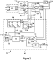
- a time to digital converter 10 is shown, which is not covered by the present invention, comprising a synchronisation block 20, charge pump 41, integrator 50 and successive approximation analog to digital converter (SAR ADC) 40.
- SAR ADC successive approximation analog to digital converter
- the synchronisation block 20 is provided with a clock reference signal 101 and with an input signal 107.
- the synchronisation block 20 converts the time difference between cycles of the clock reference signal 101 and the input signal 107 into output pulses 110, with duration based on the time difference between respective cycles of the clock reference signal and input signal.
- the synchronisation block 20 may provide an output pulse 110 with duration based on the timing difference between rising edges of the clock reference signal 101 and the input signal 107.
- the output pulses 110 are provided to the charge pump 41.
- the charge pump 41 converts the output pulses 110 into an output current pulse 111 with duration substantially proportional to the time delay.
- the output current pulse from the charge pump 41 is input to the integrator 50, which integrates the charge on the capacitor 24.
- the integrator 50 comprises a transconductance amplifier 25 with feedback capacitance. The output voltage from the transconductance amplifier 25 depends on the integral of the current output from the charge pump 41 (i.e. the total charge output from the charge pump 41).
- the output from the integrator 50 is provided to the SAR ADC 40, which converts the integrated charge on the capacitor 24 into a digital output value 125 by successive approximation (i.e. using a binary search approach, determining the most significant bit first, and successively approximating each bit in order of significance).
- the integrator 50 comprises a differential arrangement. More detail of an example architecture for the SAR ADC 40 is shown. The skilled person will appreciate that other implementations of the SAR ADC 40 and integrator 50 are possible, and that this example is merely illustrative.
- the time to digital converter 10 comprises a synchronisation block 20, charge pump 41, integrator 50 and successive approximation analog to digital converter (SAR ADC) 40.
- the charge pump 41 comprises a first current source 22 that is configured to output current pulse 111 and a second current source 21 that is configured to output current pulse 112.
- the current sources 21, 22 provide a current output when the output pulse 110 from the synchronisation block 20 is high, and no current output when the output pulse 110 is low.
- the current outputs 111, 112 of the charge pump 41 are respectively connected to non-inverting and inverting inputs of a transconductance amplifier 25 of the integrator 50.
- the charge pump 41 is operable to enable the amplitude of the output of the current pulses 111, 112 from each individual current source 21, 22 to be varied in response to an input charge pump control signal 113. This allows the resolution of the TDC 10 to be selectable, as will be explained in more detail below with reference to figure 8 .
- the charge pump control signal 113 may be a digital signal.
- the transconductance amplifier 25 comprises an inverting output 115a and a non-inverting output 115b. The difference between the inverting and non-inverting outputs 115a, 115b is the integrator output voltage 115.
- a first integrating capacitor 24 is connected between the inverting output 115a and the non-inverting input of the transconductance amplifier 25 and a second integrating capacitor 23 is connected between the non-inverting output 115b and the inverting input of the transconductance amplifier 25.
- the current pulses 111 and 112 are integrated by the transconductance amplifier 25 as charges on integrating capacitors 23 and 24 respectively.
- Charge on integrating capacitor 23 results in an output voltage 115b of opposite polarity to the output voltage 115a resulting from charge on integrating capacitor 24.
- the integrator output voltage output 115 from the transconductance amplifier is the differential of the output voltages 115a and 115b.
- a common mode voltage 114 at the integrator outputs 115a, 115b is controlled by a common-mode feedback block 26.
- the common mode feedback block 26 determines whether a common mode voltage is present at the differential outputs 115a, 115b of the transconductance amplifier.
- a common mode voltage indicates an imbalance in the amplitude of the charge output from current sources 22, 21 (and/or between the capacitors 23, 24).
- the common-mode feedback block 26 acts to cancel any imbalance by varying the output current from one of the current sources 22, 21, based on the common mode voltage at the differential outputs of the integrator 50.
- the common-mode feedback block 26 is varying the amplitude of the output of the first current source 22, but in other embodiments the output of the second current source 21 may be varied to reject a common mode voltage at differential outputs of the integrator 50 (so as to balance the negative and positive sides of the integrator 50).
- the SAR ADC 40 comprises: comparator 31, AND gate 35, control logic 30, flip-flop 33, XOR gate 33, DAC 29 and shift register 32.
- a second switch 27 is provided, configured to control connection of the DAC 29 with the inputs of the transconductance amplifier 25.
- a first switch 28 is provided, configured to provide a common mode voltage 116 to the inputs of the transconductance amplifier 25 and to the DAC 29 during resetting.
- the integrator output voltage 115 is provided to the comparator 31 (which is a 1-bit comparator) of the successive approximation register 40. Specifically, the inverting output 115a is provided to a inverting input of the comparator 31 and the non-inverting output 115b is provided to an non-inverting input of the comparator 31.
- the comparator 31 provides a high output from the non-inverting output 122 when voltage 115b is lower than voltage 115a (i.e. when the output voltage 115 is positive) and a low output from the non-inverting output when voltage 115a is lower than voltage 155b (i.e. when output voltage 115 is negative).
- the inverting and non-inverting outputs 124, 122 of the comparator 31 are connected to AND gate 35, which outputs a comparator ready signal 123 (active low). Since the comparator 31 is a clocked comparator, both outputs will be high when the clock signal 121 that is provided to the comparator is low. When the comparator reader signal 123 is high, the comparator is inactive.
- the non-inverting output 122 is provided to control logic block 30.
- the control logic block 30 controls the DAC 29, provides the clock signal 121 to the comparator 31, and controls the switching of the first and second switches 28, 27.
- the control logic 30 may be asynchronous with the clock reference signal 101 and input signal 107.
- the control logic 30 provides a digital input 155 to the DAC 29.
- the DAC 29 comprises a first switched capacitor bank (not shown in figure 1 ), which provides a current 118 based on the digital input 115, and a second switched capacitor bank, which provides a current 117 based on the digital input 155.
- the output 118 from the first DAC bank is connected to the inverting input of the transconductance amplifier 25 via the second switch 27 and the output 117 from the second DAC bank is connected to the non-inverting input of the transconductance amplifier 25 via the second switch 27.
- Connecting the first and second and DAC banks to the integrator capacitors 24, 23 varies the voltage on the first integrator capacitor 24 and the second integrator capacitor 23 by an amount based on the digital input 155 to the DAC 29.
- the currents 117 and 118 are respectively caused by redistribution of charge from the integrator capacitors 24 and 23 onto the respective switched capacitor DAC bank.
- the control logic 30 is configured to search for a configuration of each DAC bank that causes just enough current to flow from (or to) the integrator capacitors 23, 24 to reduce the output 115 of the integrator to within less than a least significant bit of zero.
- the sequence of switching the capacitors of the DAC banks will be described below in more detail with reference to figures 4 , 5 and 6 .
- each bank of the DAC 29 comprises a switched capacitor network of parallel capacitances.
- the DAC has 10 bits of resolution (but other resolutions are contemplated, e.g. from 2 bit to 24 bit).
- One electrode of each effective capacitance of the network is connected at one end to an output rail 118, and at the other end to an input corresponding with a bit of the digital input 155. Buffers may be used to drive the larger capacitors (e.g. C256).
- the effective capacitance connected to each bit of the digital inputs (D0 to D9) is doubled with each bit, so that the effective capacitance connected to the least significant bit (LSB) D0 is a factor of 512 less than the effective capacitance connected to the most significant bit (MSB) D9.
- the capacitance connected to the least significant bit comprises a series combination of capacitors C1 with capacitance equal to one nominal unit, thereby providing an effective capacitance of C0.5.
- the capacitor C256 connected to the most significant bit D9 has a capacitance of 256 times the nominal unit of capacitance.
- the current flowing to or from the DAC from the integrator capacitor 23 is therefore controlled by the digital input 155, which sets the voltages on one electrode of each capacitor C1 to C256 to high or low.
- the shift register 32 is configured to read and store the output 125 of the SAR ADC.
- the shift register 32 receives an output from the comparator 31, in this embodiment the inverting output 124. In other embodiments the shift register 32 may receive the non-inverting output 122 from the comparator 31.
- the value of the output of the comparator 31 corresponds with whether the current bit under test should be a 0 or a 1 in the output from the SAR ADC 40 (as will be explained in more detail with reference to figures 5 and 6 ).
- the shift register 32 stores the value of the current bit (0 or 1), and then shifts the value in the register 32 in response to a clock input based on the comparator ready signal 123, ready to receive the next bit value.
- the flip-flop 33 and XOR gate 34 are configured to control the first switch 28 and second switches 27, based on the output pulse from the synchronisation block 20 and a ready signal 143 from the control logic 30 indicating that the successive approximation cycle for the present cycle has completed.
- the input signal 110 is connected to the reset input of the (D-type) flip-flop 33, and the Q output from the flip-flop 33 is connected to an input of the XOR gate 34.
- the D input of the flip-flop is set to 1.
- the other input of the XOR gate 34 is connected to the output pulse 110 from the synchronisation block 20.
- the switch control output 120 of the XOR gate 34 controls the operation of the first and second switch 28, 27, and is used to reset the control logic 30.
- the control logic 30 is triggered to reset the SAR ADC 40 when the output from the XOR gates 34 goes low.
- the switch control 120 therefore controls the connection between the DAC 29 and the integrator capacitors 24, 25, and the connection between the DAC 29 and the common mode voltage input 116.
- switch control 120 When switch control 120 is high, the DAC banks are connected to the capacitors 24, 25 of the integrator 50. When the switch control 120 is low, the DAC banks are reset by connecting them to the common mode voltage input 116. The SAR ADC 40 is thereby configured to reset the DAC 29 at the end of the successive approximation cycle provided that the current pulse 110 is low. At the end of the cycle the timing of the switching is:
- the TDC 10 is configured such that the charge on the integrator 50 following the successive approximation cycle is not reset, but is left in place. This leaves an amount of charge that is less than the least significant bit on the integrator 50, which has the effect of dithering the quantisation levels of the SAR ADC 40, thereby providing for advantageous quantisation noise shaping and facilitating subsequent quantisation noise cancellation (for example by low pass filtering). Retaining the residual charge on the integrator 50 after successive approximation may thereby improve the performance of a phase locked loop comprising a SAR TDC 10 according to an embodiment.
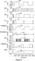
- FIG. 4 shows (from top to bottom), the clock reference input 101, the input signal 107, the re-clocked reference signal 108, the output pulse 110 (from the charge pump 41), the switch control 120, the integrator voltage output 115, the comparator clock 121, the (control logic) ready 143 and the SAR ADC output value 125.
- the clock reference input 101 is a square wave, and is not in phase with the input signal 107.
- the frequency of the input signal 107 in this example is a multiple of the clock reference frequency.
- the re-clocked reference signal 108 is at the same frequency as the clock reference input, but the edges are re-clocked by synchronisation block 20 using the input signal 107.
- the output pulse 110 from the synchronisation block 20 is high during the time between a leading edge of the clock reference input 101 and the next leading edge of the input signal 107.
- the integral of the voltage of each pulse 110 from the synchronisation block 20 therefore corresponds with the time delay (or phase difference) between the corresponding cycles of the clock reference 101 and input 107.
- the charge pump 41 converts this voltage pulse into a current pulse that charges the integrator capacitors 23, 24, integrating the current pulse. This charging of the integrator capacitors 23, 24 can be seen in the integrator voltage output 115 waveform.
- the output pulse waveform 110 is high, current is being integrated on the capacitors 23, 24, increasing the voltage output 115 from the integrator (in proportion to the amplitude of the current supplied by the charge pump 41 and the duration of the pulse). Changing the amplitude of the current output from the charge pump 41 will change the rate of charging of the capacitors 23, 24 of the integrator 50, which will have the effect of varying the timing value associated with each bit of the DAC 30.
- Varying the current amplitude from the charge pump 41 therefore provides selectable resolution of the SAR TDC 10, with a concomitant trade-off in the full scale range of the DAC 30, which affects the maximum time delay that can be approximated by the SAR ADC 40 in a single conversion cycle.
- the SAR TDC 10 may include a gain normalisation block (not shown) that normalises the digital output 125 from the SAR TDC 10 to provide a normalised SAR TDC output that corresponds with the time delay.
- the gain normalisation block may compensate for changes in the amplitude of the output current from the charge pump 41.
- the switch control 120 connects the DAC banks to the inputs of the integrator 50, and the control logic 30 determines the digital settings for the DAC 29 that reduce the voltage output from the integrator 50 to within a least significant bit (or less) of zero.
- control logic 30 may start with the MSB D9 high, so as to reduce the charge on the capacitors 23, 24 by an amount corresponding with the MSB when the DAC 29 is connected by the second switch 27 to the integrator inputs.
- the first conversion cycle of figure 4 (at approximately 32 to 45ns), is shown more clearly in figure 5 .
- the output of the integrator 50 settles (to around 35mV).
- the comparator 31 is provided with a clock signal 120, which results in the comparator 31 providing a signal 122 to the control logic 30 that indicates whether the output 115 from the integrator is positive.
- the output 115 is still positive following this, so the next most significant bit D8 is switched high by the control logic 30. In the case of the first conversion cycle, this results in enough current flow to swing the integrator output 115 negative (to approximately -65mV).
- control logic 30 switches bit D8 low, at the same as switching D7 high. This saves a step in the conversion cycle (which would otherwise be incurred if D8 was switched low without at the same time switching D7 high). Although advantageous in improving the speed of conversion, this returning of the previous bit at the same time as switching the present bit is not essential.
- the control logic 30 is configured to successively test each bit (D9 to D0) of the DAC 29 against the charge on the integrator capacitors 24, 23 which will reduce the output of the integrator 50 to an amount representing the least significant bit of the DAC 29 (or less).
- control logic 30 When the control logic 30 has completed the successive approximation cycle, it is configured to output ready signal 143, which indicates that switch control 120 can toggle the first and second switches 28, 27 so as to reset the DAC 29 ready for another conversion cycle.
- the value from the SAR ADC register 125 for the preceding conversion cycle is available on the next edge of the re-clocked reference signal 108.
- the control logic 30 may be configured to implement this method.
- the integrator 50 may be disconnected from the DAC 29 (e.g. using the second switch 27) and the MSB of the DAC 29 reset to 0.
- the integrator 50 may then be re-connected to the DAC 29 (e.g. via switch 27) and the MSB bit switched to 1, thereby reducing the output from the integrator 50 by an amount associated with the MSB before the conversion cycle begins.
- the integrator 50 is thereby effectively negatively pre-charged (relative to the charge input from the charge pump 41). In figure 6 this MSB negative pre-charge has been applied at the end of the first conversion cycle T1.
- Embodiments of the SAR TDC 10 are particularly useful in phase locked loops.
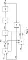
- Figure 7 shows an all-digital phase locked loop (ADPLL) including a SAR TDC 10 according to an embodiment.
- ADPLL all-digital phase locked loop
- the ADPLL comprises the SAR TDC 10, a quantisation noise cancelling block 11, a digital loop filter 12, digitally controlled oscillator 13 (DCO), frequency divider 14, divider control 15.
- DCO digitally controlled oscillator
- a clock reference input 101 and an input signal 107 is provided to the SAR TDC 10.
- the SAR TDC determines the time difference between the clock reference input 101 and the input signal 107.
- the input signal 107 is the output from the frequency divider 14.
- the frequency divider 14 receives the DCO 13 output 106 (which is the output of the phase locked loop) and divides the frequency thereof, so that a relatively low frequency reference clock input 101 may be used to generate a relatively high frequency output signal 106 with precision.
- the frequency divider 14 is controlled by the divider control block 15, which may comprise a sigma-delta modulator, so that the divider 14 and control block 15 together provide for fractional frequency dividing (as is known in the art).
- the divider control block 15 provides a divider value 105 to the divider block 14 and an accumulated sigma-delta error 104 to the quantisation noise cancelling block 11.
- the divider control block 15 is configured to receive a normalised tuning word (NTW) 103, and then to control the divider block 14 to provide the desired output frequency from the ADPLL (with reference to the reference clock 101).
- the divider control block 15 receives the re-clocked reference signal 108 from the SAR TDC 10 and the frequency divided DCO signal output by the divider block 14.
- a normalised SAR TDC output 109 from the SAR TDC 10 is provided to the quantisation noise cancelled block 11, after the addition of a phase offset signal 102.
- the quantisation noise cancelling block 11 is configured to reduce divider quantisation noise.
- the quantisation noise cancelling block 11 may be configured to cancel or reduce noise in the digital domain.
- the output 132 of the quantisation noise cancelling block 11 is the phase error 132, which is provided to the digital loop filter 12.
- the digital loop filter 12 is configured to convert the phase error input signal 132 into a digital output for controlling the DCO 13 so as to minimise the phase error 132.
- Figure 8 illustrates the operation of the ADPLL of figure 7 with reference to the variable current amplitude modes of operation of the charge pump 41.
- the SAR TDC 10 may be operated in a first mode (tracking mode), having a first current source current output amplitude and a second mode (acquisition mode), having a second, smaller charge pump output current amplitude.
- the first mode the timing resolution of the SAR TDC 10 is greater, because each bit of charge moved by the ADC 29 corresponds with a smaller increment of time. This is accompanied by a corresponding reduction in the full scale time difference value of the SAR TDC 10.
- the phase error during the tracking mode is small the SAR ADC 40 will not saturate (it is able to cancel the integrated current).
- the timing resolution of the SAR TDC 10 is lower but the full scale time difference that can be quantised by the SAR ADC 40 is larger.
- the second mode is therefore more suitable for acquiring phase lock, and the first mode is more suitable for tracking, once phase lock has been achieved.
- FIG 9 shows a phase error 132, a quantisation noise cancelling filter value 133, the SAR TDC output value 125 (without normalisation to compensate for changes in the charge pump output current), the charge pump control signal 113 and the SAR scale factor value 134.
- the SAR scale factor value 134 is used to normalise the output of the SAR TDC 10 to provide a signal that indicates the time delay (independent of the charge pump current).
- the ADPLL is acquiring phase lock on the reference signal, and the SAR TDC 10 is accordingly operating in the second (acquisition) mode, in which the charge pump current is relatively low.
- the SAR TDC 10 is switched to the first (tracking) mode, by changing the value of the charge pump control signal 113, increasing the charge pump current. This results in a step change in the raw output from the SAR TDC 125, which is compensated for by a change in the SAR scale factor value 134.
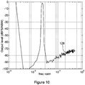
- Figure 10 shows an example of quantisation noise from a SAR TDC 10 according to an embodiment.
- the noise is plotted in dB relative to a full scale per noise bin (per noise resolution bandwidth (NBW)).
- the NBW for the graph is 0.00293.
- the charge pump current is 30 ⁇ A
- the reference frequency input is 40MHz
- full scale output from the SAR TDC corresponds with a 3.6ns time delay
- the resolution of the SAR TDC is 11.4ps.
- the SAR TDC quantisation noise 128 at high offset frequencies can be suppressed below a typical frequency controlled oscillator thermal noise by an appropriate digital loop filter. According to an embodiment, a high resolution TDC with low noise is therefore provided.
- FIG 11 illustrates the phase noise performance of a SAR TDC 10 according to an embodiment in a phase locked loop according to figure 7 .
- SAR TDC quantisation noise 130 is shown with expected voltage controlled oscillator noise 131, and a simulation of VCO phase noise 129 that includes flicker noise.
- the VCO frequency is 4.665GHz and the resolution bandwidth is 38.35 dB (with the noise plotted in dBc/Hz).
- the SAR TDC quantisation 130 is well below the noise of the VCO 129, 131 throughout the range of frequency offsets shown.
- Figure 12 shows a phase locked loop according to an embodiment, comprising a time to digital converter (TDC) 10 according to one embodiment, quantisation noise cancelling block 11, digital loop filter 12, frequency controlled oscillator 42, frequency divider 14, divider control 15, chirp control block 45, look up table 43 and digital to analog converter (DAC) 44.
- TDC time to digital converter
- DAC digital to analog converter
- a clock reference input 101 and an input signal 107 is provided to the TDC 10.
- the TDC 10 may be a SAR TDC as described above, but this is not essential and any TDC architecture may be used.
- the TDC 10 determines the time difference between the clock reference input 101 and the input signal 107.
- the input signal 107 is the output from the frequency divider 14.
- the frequency divider 14 receives the frequency controlled oscillator 42 output 106 (which is the output of the phase locked loop) and divides the frequency thereof, so that a relatively low frequency reference clock input 101 may be used to generate a relatively high frequency output signal 106 with precision.
- the frequency divider 14 is controlled by the divider control block 15, which may comprise a sigma-delta modulator, so that the divider 14 and control block 15 together provide for fractional frequency dividing (as is known in the art).
- the divider control block 15 provides a divider value 105 to the divider block 14 and an accumulated sigma-delta error 104 to the quantisation noise cancelling block 11.
- the divider control block 15 is configured to receive the divider value from the chirp control block 45.
- the divider control block 15 receives the re-clocked reference signal 108 from the SAR TDC 10 and the frequency divided DCO signal output by the divider block 14.
- the chirp control block 45 receives a normalised tuning word (NTW) 103 and controls the operation of the divider control block 15 and the operating mode of the phase locked loop, as will be explained in more detail below.
- NW normalised tuning word
- a normalised TDC output 109 from the TDC 10 is provided to the quantisation noise cancelled block 11, after the addition of a phase offset signal 102.
- the quantisation noise cancelling block 11 is configured to reduce divider quantisation noise.
- the quantisation noise cancelling block 11 may be configured to cancel or reduce noise in the digital domain.
- the output 132 of the quantisation noise cancelling block 11 is the phase error 132, which is provided to the digital loop filter 12.
- the digital loop filter 12 is configured to convert the phase error input signal 132 into a digital output for controlling the frequency controlled oscillator 42 so as to minimise the phase error 132.
- the frequency controlled oscillator 42 has a first control input, comprising a tracking input 135 and an acquisition input 136 and a second control input 139 (or frequency modulation input).
- the first control input comprises digital inputs.
- Each of the tracking input 135 and acquisition input 136 may be associated with a switched capacitor varactor bank, which are used to vary the frequency of the oscillator 42.
- the second control input 139 is an analog input, and is associated with an analog varactor. The use of an analog varactor allows filtering of quantisation noise prior to this control input, which improves the linearity of a chirp produced using the phase locked loop.
- the DAC 44 is connected to the second control input 139 of the frequency controlled oscillator 42.
- the DAC receives a digital input 142, 138 from the look up table 43 or digital loop filter 12.
- the chirp generator 45 is configured to control the operation of the phase locked loop, providing the divider value 105 to the divider control block 15, a frequency modulation control signal 140 to the look up table and a chirp window output signal 141.
- the chirp generator 45 is configured to control the phase locked loop in response to a normalised tuning word 103 input.
- the look up table (LUT) 43 is configured to receive the frequency modulation control signal 140 from the chirp generator 45.
- the LUT 43 is further configured to receive an output 138 from the loop filter 12 and to provide a digital output 142 to the DAC 44 so as to provide the second control input 139 to the frequency controlled oscillator 42.
- the LUT 43 comprises a memory for storing digital control values and, optionally, an associated chirp frequency value.
- the phase locked loop is configured not to remove the effect of the second control input 139 on the output 106 from the frequency controlled oscillator 42 in the feedback path to the TDC 10.
- the DAC 44 is responsive to the output 138 of the loop filter 12.
- the phase locked loop is thereby operable to lock to each desired frequency of a chirp by varying the second control input 139.
- the chirp control block 45 varies the divider value 105 to set the desired frequency, and the second control input 139 is varied by the feedback path until the desired frequency is obtained (when the phase is locked).
- the phase locked loop has a large bandwidth, reducing locking time for each value of the calibration.
- the LUT 43 receives the digital control value 138 that corresponds with each desired chirp frequency, and stores the value.
- the LUT 32 thereby stores in a memory a list of digital control values that correspond with each desired chirp frequency.
- the digital control values compensate for any non-linearity in the response of the frequency controlled oscillator 42 to the second control input 139.
- the DAC 44 is responsive to the digital output 142 from the LUT 43.
- the LUT 43 receives a frequency modulation control signal 140 from the chirp control block 45 corresponding with a desired chirp frequency, and outputs a digital signal 142 determined with reference to the list of digital control values in the memory. For instance, if the desired frequency corresponds exactly with one of the calibration frequencies, the stored value may be used directly. Interpolation (e.g. linear, cubic, spline, polynomial etc) may be used to determine digital control values 142 for intermediate desired frequencies 140 that do not correspond exactly with calibration frequencies of control values stored in the LUT memory.
- the chirp control block 45 provides a divider value 105 to the divider control block 15 that removes the effect of the second control input 139 of the frequency controlled oscillator 42.
- the first control input 135, 136 of the frequency controlled oscillator 42 maintains lock during rapid frequency sweeps, while compensating for any distortion caused by non-linearity.
- the feed-forward control based on stored values from a calibration of the response of the oscillator 42 to the second control input 139 means that the frequency chirp is highly linear and accurate.
- the bandwidth of the phase locked loop is smaller (relative to during calibration mode). However, since the feedback path of the phase locked loop is now only responsible for tracking temperature variations, the bandwidth does not need to be large.
- the frequency of such temperature variations is determined by thermal time constants, which may be on the order of a second, so a low phase locked loop bandwidth is sufficient during chirp mode. If, during operation in chirp mode, the tuning range of the tracking input 135 is exceeded, the acquisition input 136 may be used to maintain lock.
- a low pass filter (not shown) may be provided on the output of the DAC 44.
- the step response of the low pass filter is taken into account in the calibration mode, because it is in the loop.
- the low pass filter may reduce thermal noise and quantisation noise from the DAC 44.
- Figure 13 shows the operation of a phase locked loop according to an embodiment (e.g. as shown in figure 12 ), in a chirp mode.
- Figure 13 shows TDC path calibration gain 144, chirp window 141, phase locked loop control voltage 145, DAC output 139, divider value 105 and phase error 132 during operation.
- the phase locked loop locks onto the reference signal 101 and the phase error 132 drops to substantially zero.
- the DAC 44 receives from the LUT 43 a sequence of digital signals 142 corresponding with a linear increase in frequency output from the oscillator 42.
- the DAC output 139 increases in a substantially linear way during the chirp.
- the divider value 105 removes the effect of this in the feedback loop, so the divider value 105 substantially tracks the DAC output 139.
- the divider value 105 may be a digital value, so that the effect of the second control input (or DAC output) 139 on the frequency controlled oscillator 42 is removed in the digital domain.
- the phase locked loop remains in lock both during the chirp window, and during the reset period of the chirp, with very low phase error 132.
- the gain calibration 144 of the TDC is not affected by the rapid changes in the output frequency of the phase locked loop, because these changes are removed in the feedback loop using the divider 14.
- the divider noise cancellation (by the quantisation noise cancellation block 11) is likewise not affected by the chirp operation: the phase error remains very well controlled throughout both the chirp window and reset periods.
Landscapes
- Engineering & Computer Science (AREA)
- Physics & Mathematics (AREA)
- General Physics & Mathematics (AREA)
- Radar, Positioning & Navigation (AREA)
- Remote Sensing (AREA)
- Computer Networks & Wireless Communication (AREA)
- Theoretical Computer Science (AREA)
- Analogue/Digital Conversion (AREA)
- Stabilization Of Oscillater, Synchronisation, Frequency Synthesizers (AREA)
Claims (8)
- Zeit-Digital-Wandler (10), der Folgendes umfasst:einen Synchronisationsblock (20), der dazu ausgebildet ist, einen Spannungsimpuls mit einer Dauer basierend auf einer Zeitdifferenz zwischen einem Referenzschwingungssignal und einem Eingangsschwingungssignal auszugeben;eine Ladungspumpe (41), die eine erste Stromquelle (22) und eine zweite Stromquelle (21) umfasst, die so angeordnet sind, dass sie den Spannungsimpuls empfangen und den Spannungsimpuls in einen ersten bzw. zweiten Stromimpuls umwandeln;einen Integrator (50), der einen Transkonduktanzverstärker (25), einen ersten Integratorkondensator (24) und einen zweiten Integratorkondensator (23) aufweist;wobei der erste Integratorkondensator (24) zwischen einem invertierenden Ausgang (115a) und einem nicht-invertierenden Eingang des Transkonduktanzverstärkers angeschlossen ist, undder zweite Integratorkondensator (23) zwischen einem nicht-invertierenden Ausgang (115b) und einem invertierenden Eingang des Transkonduktanzverstärkers angeschlossen ist,der Integrator einen Eingang hat, der durch den nicht-invertierenden Eingang und den invertierenden Eingang des Transkonduktanzverstärkers gebildet wird, und einen Ausgang, der durch den invertierenden Ausgang und den nicht-invertierenden Ausgang des Transkonduktanzverstärkers gebildet wird,der Integrator ausgebildet ist, um die ersten und zweiten Stromimpulse zu empfangen und die Stromimpulse als Ladungen an den jeweiligen ersten und zweiten Integratorkondensatoren (23, 24) zu integrieren, was zu Ausgangsspannungen (115a, 115b) führt, wobei eine Integratorausgangsspannung als die Differenz der Ausgangsspannungen definiert ist, wobei eine Ladung an dem ersten Integratorkondensator (24) zu einer Ausgangsspannung mit entgegengesetzter Polarität zu der Ausgangsspannung führt, die aus einer Ladung an dem zweiten Integratorkondensator (23) resultiert; undeinen Successive Approximation-Register-Analog-Digital-Wandler (SAR ADC) (40), der so ausgebildet ist, dass er die Integrator-Ausgangsspannung bestimmt, indem er die Ladung des ersten und des zweiten Integratorkondensators (23, 24) so einstellt, dass die Integrator-Ausgangsspannung durch sukzessive Approximation auf einen Betrag verringert wird, der das niedrigstwertige Bit des DAC oder weniger repräsentiert, und der so ausgebildet ist, dass er die bestimmte Integrator-Ausgangsspannung als Digitalsignal (125) ausgibt, das den Ausgang des Zeit-Digital-Wandlers repräsentiert, wobei der SAR ADC (40) Folgendes umfasst:
einen Digital-Analog-Wandler (29), der Folgendes umfasst:eine erste geschaltete Kondensatorbank, die betriebsfähig ist, um die Ladung an dem ersten Integratorkondensator (24) einzustellen, wenn sie mit dem Eingang des Integrators (50) verbunden ist, indem sie einen Stromfluss zwischen dem ersten Integratorkondensator (24) und der ersten geschalteten Kondensatorbank basierend auf einer digitalen Eingabe veranlasst, die dem Digital-Analog-Wandler von einer Steuerlogik (30) bereitgestellt wird,eine zweite geschaltete Kondensatorbank, die betriebsfähig ist, um die Ladung an dem zweiten Integratorkondensator (23) einzustellen, wenn sie mit dem Eingang des Integrators (50) verbunden ist, indem sie einen Stromfluss zwischen dem zweiten Integratorkondensator (23) und der zweiten geschalteten Kondensatorbank basierend auf einer digitalen Eingabe veranlasst, die dem Digital-Analog-Wandler von einer Steuerlogik (30) bereitgestellt wird;einen Komparator (31), der ausgebildet ist, um den Ausgang des Integrators (50) zu testen und ein Komparatorausgangssignal basierend auf dem Ausgang des Integrators (50) bereitzustellen,wobei die Steuerlogik (30) ausgebildet ist, um das Komparator-Ausgangssignal zu empfangen und Bits zu schalten, die die ersten und zweiten geschalteten Kondensatorbänke des Digital-Analog-Wandlers (29) basierend auf dem Komparator-Ausgangssignal steuern, und um jedes der Bits sukzessive gegen die Ladung an den Integratorkondensatoren (23, 24) zu testen, um die Ausgangsspannung des Integrators (50) auf einen Betrag zu reduzieren, der das niedrigstwertige Bit des DAC oder weniger darstellt, um dadurch einen sukzessiven Approximationszyklus abzuschließen;einen ersten Schalter (28), der betriebsfähig ist, um den Digital-Analog-Wandler (29) durch Anschließen einer Gleichtaktspannung an die erste und zweite geschaltete Kondensatorbank nach jedem abgeschlossenen sukzessiven Approximationszyklus zurückzusetzen, undeinen zweiten Schalter (27), der betriebsfähig ist, um den Digital-Analog-Wandler (29) mit dem Eingang des Integrators (50) während jedes sukzessiven Approximationszyklus zu verbinden und den Digital-Analog-Wandler (29) vom Eingang des Integrators (50) zu trennen, wenn der sukzessive Approximationszyklus abgeschlossen ist, so dass der Integrator (50) nicht zurückgesetzt wird und eine Restladung beibehalten wird, die auf den ersten und zweiten Integratorkondensatoren verbleibt, wenn dem sukzessiven Approximationszyklus gefolgt wird,ein Schieberegister (32), das ausgebildet ist, um das digitale Ausgangssignal (125) des SAR ADC zu lesen und zu speichern, indem es den Wert des zu prüfenden Bits speichert und den Wert in dem Schieberegister (32) als Antwort auf eine Takteingabe basierend auf einem Komparator-Bereitschaftssignal verschiebt, bereit, den nachfolgenden Wert zu empfangen. - Zeit-Digital-Wandler (10) nach Anspruch 1, wobei die Ladungspumpe (41) ausgebildet ist, um die Amplitude des Stromimpulses als Antwort auf eine Ladungspumpen-Steuereingabe zu verändern.
- Zeit-Digital-Wandler (10) nach Anspruch 1, wobei die Steuerlogik dazu ausgebildet ist, eine Schaltsequenz für das LSB zu MSB-1 des Digital-Analog-Wandlers zu implementieren, die Folgendes umfasst:
Umschalten des Zustands des aktuellen Bits, Überprüfen des Komparator-Ausgangssignals, und falls sich der Komparator-Ausgang in einem ersten Zustand befindet, Umschalten des aktuellen Bits und des nächsten Bits, oder falls sich der Komparator-Ausgang in einem zweiten Zustand befindet, Beibehalten des Wertes des aktuellen Bits und Umschalten des nächsten Bits, wobei das nächste Bit das nächste Bit in der Reihenfolge abnehmender Wertigkeit des aktuellen Bits ist. - Zeit-Digital-Wandler (10) nach Anspruch 1, wobei die Steuerlogik dazu ausgebildet ist, am Ende eines sukzessiven Approximationszyklus Folgendes durchzuführen:
Trennen des Integrators (50) vom Digital-Analog-Wandler (29) und Festlegen des MSB auf 0, erneutes Verbinden des Integrators (50) mit dem Digital-Analog-Wandler (29) und Umschalten des MSB, Trennen des Integrators vom Digital-Analog-Wandler und Zurücksetzen des Digital-Analog-Wandlers, so dass er für den nächsten sukzessiven Approximationszyklus bereit ist, um dadurch den Dynamikbereich des Zeit-Digital-Wandlers zu vergrößern. - Phasenregelkreis, der einen digitalen Schleifenfilter, einen digital gesteuerten Oszillator und einen Zeit-Digital-Wandler gemäß einem beliebigen vorhergehenden Anspruch umfasst,
wobei der Zeit-Digital-Wandler ausgebildet ist, um eine Zeitdifferenz zwischen einem Referenztakt und einem Eingangssignal basierend auf dem Ausgang des Phasenregelkreises zu bestimmen, und der digitale Schleifenfilter ausgebildet ist, um eine Steuereingabe für den digital gesteuerten Oszillator basierend auf dem Ausgang des Zeit-Digital-Wandlers bereitzustellen. - Phasenregelkreis nach Anspruch 5, der ferner einen Frequenzteiler umfasst, der dazu ausgebildet ist, die Ausgabe des Phasenregelkreises zu empfangen und das Eingangssignal an den Zeit-Digital-Wandler auszugeben; und einen Frequenzsteuerungsblock, der ausgebildet ist, um die Operation des Frequenzteilers zu steuern, wobei der Frequenzsteuerungsblock einen Sigma-Delta-Modulator für Fraktional-n-Frequenzsteuerung umfasst.
- Phasenregelkreis nach Anspruch 6, der ferner ein Modul zur Unterdrückung von Quantisierungsrauschen aufweist, das so ausgebildet ist, dass es ein Signal basierend auf dem Ausgangssignal des Zeit-Digital-Wandlers empfängt und eine Verringerung von Quantisierungsrauschen bewirkt, das durch die Quantisierung im Frequenzsteuerblock entsteht.
- Annäherungsradar, das den Phasenregelkreis nach einem der Ansprüche 5 bis 7 aufweist.
Priority Applications (3)
| Application Number | Priority Date | Filing Date | Title |
|---|---|---|---|
| EP15155327.8A EP3059857B1 (de) | 2015-02-17 | 2015-02-17 | Zeit-Digital-Wandler und Phasenregelschleife |
| CN201610073123.7A CN105897258B (zh) | 2015-02-17 | 2016-02-02 | 时数转换器和锁相环 |
| US15/041,202 US10191453B2 (en) | 2015-02-17 | 2016-02-11 | Time to digital converter and phase locked loop |
Applications Claiming Priority (1)
| Application Number | Priority Date | Filing Date | Title |
|---|---|---|---|
| EP15155327.8A EP3059857B1 (de) | 2015-02-17 | 2015-02-17 | Zeit-Digital-Wandler und Phasenregelschleife |
Publications (2)
| Publication Number | Publication Date |
|---|---|
| EP3059857A1 EP3059857A1 (de) | 2016-08-24 |
| EP3059857B1 true EP3059857B1 (de) | 2021-11-03 |
Family
ID=52469731
Family Applications (1)
| Application Number | Title | Priority Date | Filing Date |
|---|---|---|---|
| EP15155327.8A Active EP3059857B1 (de) | 2015-02-17 | 2015-02-17 | Zeit-Digital-Wandler und Phasenregelschleife |
Country Status (3)
| Country | Link |
|---|---|
| US (1) | US10191453B2 (de) |
| EP (1) | EP3059857B1 (de) |
| CN (1) | CN105897258B (de) |
Families Citing this family (34)
| Publication number | Priority date | Publication date | Assignee | Title |
|---|---|---|---|---|
| US10582608B2 (en) * | 2016-07-20 | 2020-03-03 | Hcl Technologies Limited | Interconnection between printed circuit boards |
| US9746832B1 (en) | 2016-09-09 | 2017-08-29 | Samsung Electronics Co., Ltd | System and method for time-to-digital converter fine-conversion using analog-to-digital converter (ADC) |
| US10009036B2 (en) | 2016-09-09 | 2018-06-26 | Samsung Electronics Co., Ltd | System and method of calibrating input signal to successive approximation register (SAR) analog-to-digital converter (ADC) in ADC-assisted time-to-digital converter (TDC) |
| US10520583B2 (en) * | 2016-10-25 | 2019-12-31 | GM Global Technology Operations LLC | Chirp modulation via chirp slope switching |
| EP3327461B1 (de) * | 2016-11-23 | 2020-11-04 | NXP USA, Inc. | Digitaler synthesizer, radarvorrichtung und verfahren dafür |
| WO2018094681A1 (zh) * | 2016-11-25 | 2018-05-31 | 深圳市汇顶科技股份有限公司 | I-v转换模块 |
| EP3343774B1 (de) | 2016-12-30 | 2020-07-22 | Nxp B.V. | Digital gesteuerter oszillator |
| WO2019146177A1 (ja) * | 2018-01-25 | 2019-08-01 | ソニーセミコンダクタソリューションズ株式会社 | 時間デジタル変換回路および位相同期回路 |
| JP7346379B2 (ja) * | 2018-03-02 | 2023-09-19 | ソニーセミコンダクタソリューションズ株式会社 | 位相同期回路 |
| US10516401B2 (en) | 2018-03-09 | 2019-12-24 | Texas Instruments Incorporated | Wobble reduction in an integer mode digital phase locked loop |
| US10498344B2 (en) | 2018-03-09 | 2019-12-03 | Texas Instruments Incorporated | Phase cancellation in a phase-locked loop |
| US10516402B2 (en) | 2018-03-09 | 2019-12-24 | Texas Instruments Incorporated | Corrupted clock detection circuit for a phase-locked loop |
| US10686456B2 (en) | 2018-03-09 | 2020-06-16 | Texas Instruments Incorporated | Cycle slip detection and correction in phase-locked loop |
| US10491222B2 (en) | 2018-03-13 | 2019-11-26 | Texas Instruments Incorporated | Switch between input reference clocks of different frequencies in a phase locked loop (PLL) without phase impact |
| US10505555B2 (en) | 2018-03-13 | 2019-12-10 | Texas Instruments Incorporated | Crystal oscillator offset trim in a phase-locked loop |
| US10496041B2 (en) | 2018-05-04 | 2019-12-03 | Texas Instruments Incorporated | Time-to-digital converter circuit |
| US10505554B2 (en) | 2018-05-14 | 2019-12-10 | Texas Instruments Incorporated | Digital phase-locked loop |
| US11017184B2 (en) * | 2018-10-26 | 2021-05-25 | Sendyne Corporation | Runtime-calibratable analog computing system and methods of use |
| CN109299572B (zh) * | 2018-10-29 | 2022-11-08 | 成都师范学院 | 荷控忆阶元 |
| US10826387B2 (en) | 2018-11-27 | 2020-11-03 | Nxp B.V. | Charge pump and method for operating a charge pump |
| CN109861691B (zh) * | 2019-01-02 | 2020-08-28 | 西安电子科技大学 | 基于延迟锁相环的两步式混合结构sar tdc的模数转换器电路 |
| US10886905B1 (en) * | 2019-01-24 | 2021-01-05 | Dialog Semiconductor B.V. | Signal generator with coherent phase output |
| IT201900008793A1 (it) | 2019-06-13 | 2020-12-13 | Fond Bruno Kessler | Modulo circuitale di alimentazione per tdc e metodo di calibrazione di detto modulo circuitale di alimentazione |
| US10826514B1 (en) | 2019-10-15 | 2020-11-03 | Ciena Corporation | Noise-shaping enhanced gated ring oscillator based analog-to-digital converters |
| CN112737579A (zh) * | 2019-10-28 | 2021-04-30 | 瑞昱半导体股份有限公司 | 次采样锁相回路 |
| EP3836401A1 (de) | 2019-12-10 | 2021-06-16 | NXP USA, Inc. | Frequenzsynthesizer mit phasenrauschtemperaturkompensation, kommunikationseinheit und verfahren dafür |
| KR102317072B1 (ko) * | 2019-12-17 | 2021-10-25 | 현대모비스 주식회사 | 라이다 시스템에서의 시간-디지털 변환 방법 및 장치 |
| US11067954B1 (en) | 2020-07-15 | 2021-07-20 | Analog Devices International Unlimited Company | Time-to-digital converters with low area and low power consumption |
| US11729880B1 (en) | 2020-08-31 | 2023-08-15 | Apple Inc. | Arbitrary waveform generator for current-controlled elements in portable electronic devices |
| US11843387B1 (en) | 2020-08-31 | 2023-12-12 | Apple Inc. | Tx-Rx synchronization for reflective optoelectronic systems in portable electronic devices |
| US11641206B2 (en) * | 2021-01-07 | 2023-05-02 | AyDeeKay LLC | Digitally calibrated programmable clock phase generation circuit |
| US11632105B2 (en) | 2021-03-31 | 2023-04-18 | Analog Devices International Unlimited Company | Fast overcurrent detection in battery management system |
| CN114200287B (zh) * | 2021-12-06 | 2024-03-29 | 广东利扬芯片测试股份有限公司 | 一种dTof芯片的脉冲波形处理电路 |
| CN114967411B (zh) * | 2022-06-23 | 2024-01-16 | 西北工业大学 | 一种具备自动复位机制的多级时间数字转换器 |
Family Cites Families (20)
| Publication number | Priority date | Publication date | Assignee | Title |
|---|---|---|---|---|
| US7119727B2 (en) * | 2004-10-25 | 2006-10-10 | Atmel Corporation | Analog-to-digital converter |
| US7522011B2 (en) | 2005-08-15 | 2009-04-21 | Nokia Corporation | High pass modulation of a phase locked loop |
| US7535311B2 (en) | 2006-11-30 | 2009-05-19 | Infineon Technologies Ag | Direct wideband modulation of a frequency synthesizer |
| CN101667832B (zh) * | 2008-05-13 | 2013-05-29 | 瑞昱半导体股份有限公司 | 分数-n锁相装置与方法 |
| US8169265B2 (en) | 2009-04-29 | 2012-05-01 | Mediatek Inc. | Phase lock loop circuits |
| WO2011002944A1 (en) * | 2009-06-30 | 2011-01-06 | Qualcomm Incorporated | Adc-based mixed-mode digital phase-locked loop |
| US8339165B2 (en) * | 2009-12-07 | 2012-12-25 | Qualcomm Incorporated | Configurable digital-analog phase locked loop |
| US8274339B2 (en) | 2010-04-29 | 2012-09-25 | Intel Corporation | Automatic frequency control architecture with digital temperature compensation |
| US8106808B1 (en) * | 2010-07-21 | 2012-01-31 | Applied Micro Circuits Corporation | Successive time-to-digital converter for a digital phase-locked loop |
| KR101300828B1 (ko) * | 2010-12-23 | 2013-08-29 | 건국대학교 산학협력단 | Sar 기법을 이용한 타임-투-디지털 컨버터 및 그 방법 |
| US8634512B2 (en) * | 2011-02-08 | 2014-01-21 | Qualcomm Incorporated | Two point modulation digital phase locked loop |
| WO2012153375A1 (ja) * | 2011-05-06 | 2012-11-15 | 富士通株式会社 | クロック生成回路 |
| US8471751B2 (en) * | 2011-06-30 | 2013-06-25 | Intel Corporation | Two-stage analog-to-digital converter using SAR and TDC |
| KR101214976B1 (ko) * | 2011-11-01 | 2012-12-24 | 포항공과대학교 산학협력단 | 델타-시그마 변조방식을 이용한 노이즈 세이핑 시간-디지털 변환기 |
| JP5616948B2 (ja) * | 2012-02-16 | 2014-10-29 | 株式会社半導体理工学研究センター | マルチビットのデルタシグマ型タイムデジタイザ回路及びその校正方法 |
| US8618967B2 (en) * | 2012-03-30 | 2013-12-31 | Broadcom Corporation | Systems, circuits, and methods for a sigma-delta based time to digital converter |
| CN103078644B (zh) * | 2012-12-31 | 2016-02-10 | 东南大学 | 时间数字转换器 |
| CN103560786B (zh) * | 2013-11-21 | 2017-07-28 | 东南大学 | 一种全数字逐次逼近寄存器式快速锁定延时锁定环 |
| US9041444B1 (en) * | 2013-11-27 | 2015-05-26 | Broadcom Corporation | Time-to-digital convertor-assisted phase-locked loop spur mitigation |
| US9425815B2 (en) * | 2015-01-20 | 2016-08-23 | Taiwan Semiconductor Manufacturing Company, Ltd. | Hybrid pipelined analog-to-digital converter |
-
2015
- 2015-02-17 EP EP15155327.8A patent/EP3059857B1/de active Active
-
2016
- 2016-02-02 CN CN201610073123.7A patent/CN105897258B/zh active Active
- 2016-02-11 US US15/041,202 patent/US10191453B2/en active Active
Non-Patent Citations (1)
| Title |
|---|
| None * |
Also Published As
| Publication number | Publication date |
|---|---|
| CN105897258B (zh) | 2021-02-05 |
| CN105897258A (zh) | 2016-08-24 |
| US20160238998A1 (en) | 2016-08-18 |
| EP3059857A1 (de) | 2016-08-24 |
| US10191453B2 (en) | 2019-01-29 |
Similar Documents
| Publication | Publication Date | Title |
|---|---|---|
| EP3059857B1 (de) | Zeit-Digital-Wandler und Phasenregelschleife | |
| US9584177B2 (en) | Time to digital converter and phase locked loop | |
| US10895850B1 (en) | Mixed-domain circuit with differential domain-converters | |
| CN107046421B (zh) | 全数字锁相环及其控制方法 | |
| US9461653B2 (en) | Fractional-N phase-locked loop | |
| US8854102B2 (en) | Clock generating circuit | |
| US9319051B2 (en) | Digital PLL with hybrid phase/frequency detector and digital noise cancellation | |
| CN107666320B (zh) | 带噪声整形符号的数模转换器 | |
| EP3269040B1 (de) | Phasenregelschleife (pll)-architektur | |
| US10979059B1 (en) | Successive approximation register analog to digital converter based phase-locked loop with programmable range | |
| US10103740B2 (en) | Method and apparatus for calibrating a digitally controlled oscillator | |
| CN108092662B (zh) | 频率合成装置及其方法 | |
| TW202220386A (zh) | 鎖相環電路及其操作方法以及子範圍控制電路 | |
| US10735012B2 (en) | Digitally controlled oscillator | |
| JP2016181735A (ja) | 位相−デジタル変換器および受信機 | |
| US9019017B2 (en) | Digitally controlled oscillator and digital PLL including the same | |
| CN114244357A (zh) | 用于soc的全数字频率综合器及芯片 | |
| US10374618B1 (en) | Frequency locked loop with multi-bit sampler | |
| Ouyang et al. | A high resolution Time-to-Digital Converter (TDC) based on self-calibrated Digital-to-Time Converter (DTC) | |
| US11658666B1 (en) | Fractional-N ADPLL with reference dithering | |
| Vesely et al. | PLL-SAR: A New High-Speed Analog to Digital Converter Architecture | |
| CN117559993A (zh) | 一种电荷舵鉴数字相器及其电荷舵采样全数字锁相环 | |
| KR20230077603A (ko) | 타임-디지털 컨버터 및 이를 포함하는 디지털 위상 고정 루프 회로 | |
| CN116170015A (zh) | 时间-数字转换器和包括其的数字锁相环电路 |
Legal Events
| Date | Code | Title | Description |
|---|---|---|---|
| PUAI | Public reference made under article 153(3) epc to a published international application that has entered the european phase |
Free format text: ORIGINAL CODE: 0009012 |
|
| AK | Designated contracting states |
Kind code of ref document: A1 Designated state(s): AL AT BE BG CH CY CZ DE DK EE ES FI FR GB GR HR HU IE IS IT LI LT LU LV MC MK MT NL NO PL PT RO RS SE SI SK SM TR |
|
| AX | Request for extension of the european patent |
Extension state: BA ME |
|
| STAA | Information on the status of an ep patent application or granted ep patent |
Free format text: STATUS: REQUEST FOR EXAMINATION WAS MADE |
|
| 17P | Request for examination filed |
Effective date: 20170224 |
|
| RBV | Designated contracting states (corrected) |
Designated state(s): AL AT BE BG CH CY CZ DE DK EE ES FI FR GB GR HR HU IE IS IT LI LT LU LV MC MK MT NL NO PL PT RO RS SE SI SK SM TR |
|
| STAA | Information on the status of an ep patent application or granted ep patent |
Free format text: STATUS: EXAMINATION IS IN PROGRESS |
|
| 17Q | First examination report despatched |
Effective date: 20190917 |
|
| STAA | Information on the status of an ep patent application or granted ep patent |
Free format text: STATUS: EXAMINATION IS IN PROGRESS |
|
| GRAP | Despatch of communication of intention to grant a patent |
Free format text: ORIGINAL CODE: EPIDOSNIGR1 |
|
| STAA | Information on the status of an ep patent application or granted ep patent |
Free format text: STATUS: GRANT OF PATENT IS INTENDED |
|
| INTG | Intention to grant announced |
Effective date: 20210730 |
|
| GRAS | Grant fee paid |
Free format text: ORIGINAL CODE: EPIDOSNIGR3 |
|
| GRAA | (expected) grant |
Free format text: ORIGINAL CODE: 0009210 |
|
| STAA | Information on the status of an ep patent application or granted ep patent |
Free format text: STATUS: THE PATENT HAS BEEN GRANTED |
|
| AK | Designated contracting states |
Kind code of ref document: B1 Designated state(s): AL AT BE BG CH CY CZ DE DK EE ES FI FR GB GR HR HU IE IS IT LI LT LU LV MC MK MT NL NO PL PT RO RS SE SI SK SM TR |
|
| REG | Reference to a national code |
Ref country code: GB Ref legal event code: FG4D |
|
| REG | Reference to a national code |
Ref country code: AT Ref legal event code: REF Ref document number: 1444899 Country of ref document: AT Kind code of ref document: T Effective date: 20211115 Ref country code: CH Ref legal event code: EP |
|
| REG | Reference to a national code |
Ref country code: DE Ref legal event code: R096 Ref document number: 602015074610 Country of ref document: DE |
|
| REG | Reference to a national code |
Ref country code: IE Ref legal event code: FG4D |
|
| REG | Reference to a national code |
Ref country code: LT Ref legal event code: MG9D |
|
| REG | Reference to a national code |
Ref country code: NL Ref legal event code: MP Effective date: 20211103 |
|
| REG | Reference to a national code |
Ref country code: AT Ref legal event code: MK05 Ref document number: 1444899 Country of ref document: AT Kind code of ref document: T Effective date: 20211103 |
|
| PG25 | Lapsed in a contracting state [announced via postgrant information from national office to epo] |
Ref country code: RS Free format text: LAPSE BECAUSE OF FAILURE TO SUBMIT A TRANSLATION OF THE DESCRIPTION OR TO PAY THE FEE WITHIN THE PRESCRIBED TIME-LIMIT Effective date: 20211103 Ref country code: LT Free format text: LAPSE BECAUSE OF FAILURE TO SUBMIT A TRANSLATION OF THE DESCRIPTION OR TO PAY THE FEE WITHIN THE PRESCRIBED TIME-LIMIT Effective date: 20211103 Ref country code: FI Free format text: LAPSE BECAUSE OF FAILURE TO SUBMIT A TRANSLATION OF THE DESCRIPTION OR TO PAY THE FEE WITHIN THE PRESCRIBED TIME-LIMIT Effective date: 20211103 Ref country code: BG Free format text: LAPSE BECAUSE OF FAILURE TO SUBMIT A TRANSLATION OF THE DESCRIPTION OR TO PAY THE FEE WITHIN THE PRESCRIBED TIME-LIMIT Effective date: 20220203 Ref country code: AT Free format text: LAPSE BECAUSE OF FAILURE TO SUBMIT A TRANSLATION OF THE DESCRIPTION OR TO PAY THE FEE WITHIN THE PRESCRIBED TIME-LIMIT Effective date: 20211103 |
|
| PG25 | Lapsed in a contracting state [announced via postgrant information from national office to epo] |
Ref country code: IS Free format text: LAPSE BECAUSE OF FAILURE TO SUBMIT A TRANSLATION OF THE DESCRIPTION OR TO PAY THE FEE WITHIN THE PRESCRIBED TIME-LIMIT Effective date: 20220303 Ref country code: SE Free format text: LAPSE BECAUSE OF FAILURE TO SUBMIT A TRANSLATION OF THE DESCRIPTION OR TO PAY THE FEE WITHIN THE PRESCRIBED TIME-LIMIT Effective date: 20211103 Ref country code: PT Free format text: LAPSE BECAUSE OF FAILURE TO SUBMIT A TRANSLATION OF THE DESCRIPTION OR TO PAY THE FEE WITHIN THE PRESCRIBED TIME-LIMIT Effective date: 20220303 Ref country code: PL Free format text: LAPSE BECAUSE OF FAILURE TO SUBMIT A TRANSLATION OF THE DESCRIPTION OR TO PAY THE FEE WITHIN THE PRESCRIBED TIME-LIMIT Effective date: 20211103 Ref country code: NO Free format text: LAPSE BECAUSE OF FAILURE TO SUBMIT A TRANSLATION OF THE DESCRIPTION OR TO PAY THE FEE WITHIN THE PRESCRIBED TIME-LIMIT Effective date: 20220203 Ref country code: NL Free format text: LAPSE BECAUSE OF FAILURE TO SUBMIT A TRANSLATION OF THE DESCRIPTION OR TO PAY THE FEE WITHIN THE PRESCRIBED TIME-LIMIT Effective date: 20211103 Ref country code: LV Free format text: LAPSE BECAUSE OF FAILURE TO SUBMIT A TRANSLATION OF THE DESCRIPTION OR TO PAY THE FEE WITHIN THE PRESCRIBED TIME-LIMIT Effective date: 20211103 Ref country code: HR Free format text: LAPSE BECAUSE OF FAILURE TO SUBMIT A TRANSLATION OF THE DESCRIPTION OR TO PAY THE FEE WITHIN THE PRESCRIBED TIME-LIMIT Effective date: 20211103 Ref country code: GR Free format text: LAPSE BECAUSE OF FAILURE TO SUBMIT A TRANSLATION OF THE DESCRIPTION OR TO PAY THE FEE WITHIN THE PRESCRIBED TIME-LIMIT Effective date: 20220204 Ref country code: ES Free format text: LAPSE BECAUSE OF FAILURE TO SUBMIT A TRANSLATION OF THE DESCRIPTION OR TO PAY THE FEE WITHIN THE PRESCRIBED TIME-LIMIT Effective date: 20211103 |
|
| PG25 | Lapsed in a contracting state [announced via postgrant information from national office to epo] |
Ref country code: SM Free format text: LAPSE BECAUSE OF FAILURE TO SUBMIT A TRANSLATION OF THE DESCRIPTION OR TO PAY THE FEE WITHIN THE PRESCRIBED TIME-LIMIT Effective date: 20211103 Ref country code: SK Free format text: LAPSE BECAUSE OF FAILURE TO SUBMIT A TRANSLATION OF THE DESCRIPTION OR TO PAY THE FEE WITHIN THE PRESCRIBED TIME-LIMIT Effective date: 20211103 Ref country code: RO Free format text: LAPSE BECAUSE OF FAILURE TO SUBMIT A TRANSLATION OF THE DESCRIPTION OR TO PAY THE FEE WITHIN THE PRESCRIBED TIME-LIMIT Effective date: 20211103 Ref country code: EE Free format text: LAPSE BECAUSE OF FAILURE TO SUBMIT A TRANSLATION OF THE DESCRIPTION OR TO PAY THE FEE WITHIN THE PRESCRIBED TIME-LIMIT Effective date: 20211103 Ref country code: DK Free format text: LAPSE BECAUSE OF FAILURE TO SUBMIT A TRANSLATION OF THE DESCRIPTION OR TO PAY THE FEE WITHIN THE PRESCRIBED TIME-LIMIT Effective date: 20211103 Ref country code: CZ Free format text: LAPSE BECAUSE OF FAILURE TO SUBMIT A TRANSLATION OF THE DESCRIPTION OR TO PAY THE FEE WITHIN THE PRESCRIBED TIME-LIMIT Effective date: 20211103 |
|
| REG | Reference to a national code |
Ref country code: DE Ref legal event code: R097 Ref document number: 602015074610 Country of ref document: DE |
|
| PLBE | No opposition filed within time limit |
Free format text: ORIGINAL CODE: 0009261 |
|
| STAA | Information on the status of an ep patent application or granted ep patent |
Free format text: STATUS: NO OPPOSITION FILED WITHIN TIME LIMIT |
|
| PG25 | Lapsed in a contracting state [announced via postgrant information from national office to epo] |
Ref country code: MC Free format text: LAPSE BECAUSE OF FAILURE TO SUBMIT A TRANSLATION OF THE DESCRIPTION OR TO PAY THE FEE WITHIN THE PRESCRIBED TIME-LIMIT Effective date: 20211103 |
|
| 26N | No opposition filed |
Effective date: 20220804 |
|
| REG | Reference to a national code |
Ref country code: CH Ref legal event code: PL |
|
| REG | Reference to a national code |
Ref country code: BE Ref legal event code: MM Effective date: 20220228 |
|
| GBPC | Gb: european patent ceased through non-payment of renewal fee |
Effective date: 20220217 |
|
| PG25 | Lapsed in a contracting state [announced via postgrant information from national office to epo] |
Ref country code: LU Free format text: LAPSE BECAUSE OF NON-PAYMENT OF DUE FEES Effective date: 20220217 Ref country code: AL Free format text: LAPSE BECAUSE OF FAILURE TO SUBMIT A TRANSLATION OF THE DESCRIPTION OR TO PAY THE FEE WITHIN THE PRESCRIBED TIME-LIMIT Effective date: 20211103 |
|
| PG25 | Lapsed in a contracting state [announced via postgrant information from national office to epo] |
Ref country code: SI Free format text: LAPSE BECAUSE OF FAILURE TO SUBMIT A TRANSLATION OF THE DESCRIPTION OR TO PAY THE FEE WITHIN THE PRESCRIBED TIME-LIMIT Effective date: 20211103 |
|
| PG25 | Lapsed in a contracting state [announced via postgrant information from national office to epo] |
Ref country code: LI Free format text: LAPSE BECAUSE OF NON-PAYMENT OF DUE FEES Effective date: 20220228 Ref country code: IE Free format text: LAPSE BECAUSE OF NON-PAYMENT OF DUE FEES Effective date: 20220217 Ref country code: GB Free format text: LAPSE BECAUSE OF NON-PAYMENT OF DUE FEES Effective date: 20220217 Ref country code: CH Free format text: LAPSE BECAUSE OF NON-PAYMENT OF DUE FEES Effective date: 20220228 |
|
| PG25 | Lapsed in a contracting state [announced via postgrant information from national office to epo] |
Ref country code: BE Free format text: LAPSE BECAUSE OF NON-PAYMENT OF DUE FEES Effective date: 20220228 |
|
| PGFP | Annual fee paid to national office [announced via postgrant information from national office to epo] |
Ref country code: FR Payment date: 20230119 Year of fee payment: 9 |
|
| PG25 | Lapsed in a contracting state [announced via postgrant information from national office to epo] |
Ref country code: IT Free format text: LAPSE BECAUSE OF FAILURE TO SUBMIT A TRANSLATION OF THE DESCRIPTION OR TO PAY THE FEE WITHIN THE PRESCRIBED TIME-LIMIT Effective date: 20211103 |
|
| P01 | Opt-out of the competence of the unified patent court (upc) registered |
Effective date: 20230725 |
|
| PG25 | Lapsed in a contracting state [announced via postgrant information from national office to epo] |
Ref country code: HU Free format text: LAPSE BECAUSE OF FAILURE TO SUBMIT A TRANSLATION OF THE DESCRIPTION OR TO PAY THE FEE WITHIN THE PRESCRIBED TIME-LIMIT; INVALID AB INITIO Effective date: 20150217 |
|
| PG25 | Lapsed in a contracting state [announced via postgrant information from national office to epo] |
Ref country code: MK Free format text: LAPSE BECAUSE OF FAILURE TO SUBMIT A TRANSLATION OF THE DESCRIPTION OR TO PAY THE FEE WITHIN THE PRESCRIBED TIME-LIMIT Effective date: 20211103 Ref country code: CY Free format text: LAPSE BECAUSE OF FAILURE TO SUBMIT A TRANSLATION OF THE DESCRIPTION OR TO PAY THE FEE WITHIN THE PRESCRIBED TIME-LIMIT Effective date: 20211103 |
|
| PGFP | Annual fee paid to national office [announced via postgrant information from national office to epo] |
Ref country code: DE Payment date: 20240123 Year of fee payment: 10 |