EP4066601B1 - Elektrisches gerät - Google Patents
Elektrisches gerät Download PDFInfo
- Publication number
- EP4066601B1 EP4066601B1 EP20812285.3A EP20812285A EP4066601B1 EP 4066601 B1 EP4066601 B1 EP 4066601B1 EP 20812285 A EP20812285 A EP 20812285A EP 4066601 B1 EP4066601 B1 EP 4066601B1
- Authority
- EP
- European Patent Office
- Prior art keywords
- circuit board
- electrical device
- housing wall
- electrically conductive
- printed circuit
- Prior art date
- Legal status (The legal status is an assumption and is not a legal conclusion. Google has not performed a legal analysis and makes no representation as to the accuracy of the status listed.)
- Active
Links
Images
Classifications
-
- H—ELECTRICITY
- H05—ELECTRIC TECHNIQUES NOT OTHERWISE PROVIDED FOR
- H05K—PRINTED CIRCUITS; CASINGS OR CONSTRUCTIONAL DETAILS OF ELECTRIC APPARATUS; MANUFACTURE OF ASSEMBLAGES OF ELECTRICAL COMPONENTS
- H05K5/00—Casings, cabinets or drawers for electric apparatus
- H05K5/0026—Casings, cabinets or drawers for electric apparatus provided with connectors and printed circuit boards [PCB], e.g. automotive electronic control units
- H05K5/0047—Casings, cabinets or drawers for electric apparatus provided with connectors and printed circuit boards [PCB], e.g. automotive electronic control units having a two-part housing enclosing a PCB
- H05K5/006—Casings, cabinets or drawers for electric apparatus provided with connectors and printed circuit boards [PCB], e.g. automotive electronic control units having a two-part housing enclosing a PCB characterized by features for holding the PCB within the housing
-
- H—ELECTRICITY
- H01—ELECTRIC ELEMENTS
- H01R—ELECTRICALLY-CONDUCTIVE CONNECTIONS; STRUCTURAL ASSOCIATIONS OF A PLURALITY OF MUTUALLY-INSULATED ELECTRICAL CONNECTING ELEMENTS; COUPLING DEVICES; CURRENT COLLECTORS
- H01R12/00—Structural associations of a plurality of mutually-insulated electrical connecting elements, specially adapted for printed circuits, e.g. printed circuit boards [PCB], flat or ribbon cables, or like generally planar structures, e.g. terminal strips, terminal blocks; Coupling devices specially adapted for printed circuits, flat or ribbon cables, or like generally planar structures; Terminals specially adapted for contact with, or insertion into, printed circuits, flat or ribbon cables, or like generally planar structures
- H01R12/50—Fixed connections
- H01R12/51—Fixed connections for rigid printed circuits or like structures
-
- H—ELECTRICITY
- H05—ELECTRIC TECHNIQUES NOT OTHERWISE PROVIDED FOR
- H05K—PRINTED CIRCUITS; CASINGS OR CONSTRUCTIONAL DETAILS OF ELECTRIC APPARATUS; MANUFACTURE OF ASSEMBLAGES OF ELECTRICAL COMPONENTS
- H05K5/00—Casings, cabinets or drawers for electric apparatus
- H05K5/02—Details
- H05K5/0247—Electrical details of casings, e.g. terminals, passages for cables or wiring
-
- H—ELECTRICITY
- H05—ELECTRIC TECHNIQUES NOT OTHERWISE PROVIDED FOR
- H05K—PRINTED CIRCUITS; CASINGS OR CONSTRUCTIONAL DETAILS OF ELECTRIC APPARATUS; MANUFACTURE OF ASSEMBLAGES OF ELECTRICAL COMPONENTS
- H05K9/00—Screening of apparatus or components against electric or magnetic fields
- H05K9/0007—Casings
- H05K9/002—Casings with localised screening
- H05K9/0039—Galvanic coupling of ground layer on printed circuit board [PCB] to conductive casing
Definitions
- the invention relates to an electrical device.
- the US 2012/119757 A1 discloses an electrical device according to the preamble of claim 1.
- the invention is based on the object of providing an electrical device that can be manufactured easily and inexpensively.
- the electrical device has a housing with a first electrically conductive housing wall.
- the electrical device further comprises a first circuit board which is arranged in the housing and which has a first electrical conductor.
- the first electrically conductive housing wall can be reversibly electrically connected to the first electrical conductor of the first circuit board by means of a screw connection.
- the first circuit board is aligned perpendicular to the first electrically conductive housing wall.
- a holder for the first circuit board is arranged on the first electrically conductive housing wall or the first electrically conductive housing wall has a holder for the first circuit board.
- the first circuit board can lie flat on the holder in the intended installation position.
- the screw connection releasably mechanically connects the first circuit board to the holder.
- the holder is electrically conductively connected to the first electrically conductive housing wall.
- the first housing wall and the holder are formed in one piece.
- the first electrically conductive housing wall and the holder are designed as a punched and bent part.
- the electrically conductive housing wall is punched in a U-shape in the predetermined area of the holder in a first processing step, wherein after punching the holder is bent inwards, i.e. the holder is then bent into the interior of the housing and then preferably stands perpendicularly on the electrically conductive housing wall.
- the holder can also be connected to the first electrically conductive housing wall by means of a soldered or welded connection.
- the electrical device has a penetration protection which closes an opening in the first electrically conductive housing wall, which is formed by the holder bent into the interior of the housing, in particular in order to achieve a predetermined degree of protection, for example IP 20 or IP 31.
- a second housing wall, in particular a cover, arranged adjacent to and perpendicular to the first housing wall can have the penetration protection.
- a screw of the screw connection has a longitudinal extension that runs perpendicular to the first circuit board.
- the electrical device has a second circuit board that runs plane-parallel to the first electrically conductive housing wall, wherein the second circuit board holds the first circuit board in addition to the holder of the first electrically conductive housing wall.
- the second circuit board can run plane-parallel to the first electrically conductive housing wall at a predetermined distance, wherein the first circuit board is mechanically fixed on one side by the holder of the first electrically conductive housing wall and is mechanically fixed on another side by the second circuit board.
- the first circuit board has a second electrical conductor.
- the electrical device also has conventional radio interference suppression components, for example radio interference suppression capacitors, radio interference suppression chokes, etc.
- the radio interference suppression components are arranged on the first circuit board and are electrically connected to the second electrical conductor.
- the second electrical conductor is/will be electrically connected to the first electrical conductor by means of the screw connection or, if a screw connection is present. Accordingly, the second electrical conductor is/will be electrically separated from the first electrical conductor when the screw connection is removed or loosened.
- the electrical device has a TT (Terre Terre) network mode or a TN (Terre Neutre) network mode as long as the first electrically conductive housing wall is connected to the first electrical conductor of the first circuit board is electrically connected by means of the screw connection. As long as the first electrically conductive housing wall is not electrically connected to the first electrical conductor of the first circuit board by means of the screw connection, the electrical device has an IT (Isnic Terre) network mode.
- the electrical device can be, for example, a power converter, particularly in the form of a frequency converter or a power feed-in unit.
- a power feed-in unit feeds electrical energy/power, which is present in an intermediate circuit, for example, back into a supply network.
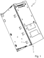
- Fig. 1 shows a perspective view of an electrical device 1, for example in the form of a frequency converter.
- the electrical device 1 has a housing 2 with a first electrically conductive housing wall 3 and further, unspecified housing walls, which together form the housing 2 of the electrical device 1.
- the electrical device 1 has a first circuit board 4 with a plurality of components arranged thereon, wherein the first circuit board 4 is arranged in the housing 2.
- the first circuit board 4 has a first electrical conductor 5 in the form of a conductor track, see Fig. 3
- the first printed circuit board 4 has, in addition to the first electrical Conductor 5 also has a plurality of further electrical conductors/conductor tracks, which, however, are not shown for reasons of better representation of the features essential to the invention.
- the first electrically conductive housing wall 3 is electrically connected to the first electrical conductor 5 of the first circuit board 4 by means of a removable screw connection 6.
- the first circuit board 4 is aligned perpendicular to the first electrically conductive housing wall 3.
- a holder 7 for the first circuit board 4 is formed on the first electrically conductive housing wall 3, wherein the first housing wall 3 and the holder 7 are embodied in one piece as a stamped and bent part.
- the holder 7 is bent into the interior of the housing 2.
- the screw connection 6 mechanically connects the first circuit board 4 to the holder 7 in a detachable manner.
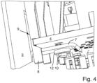
- the screw connection 6 is secured by means of a screw 10, see in particular Fig. 4 , and a nut 12 pressed into the holder 7, wherein the screw 10 engages through an associated opening in the circuit board 4, then through an associated opening in the holder 7 into the nut 12. It is understood that a screw head of the screw 10 has a diameter that is larger than the opening in the circuit board. In its screwed-in state, the screw 10 has a longitudinal extension that runs perpendicular to the first circuit board 4.
- the electrical device 1 has a penetration protection 8 which closes an opening 9 in the first electrically conductive housing wall 3, which is formed by the holder 7 bent into the interior of the housing 2.
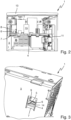
- the penetration protection 8 can be part of a cover 13, see Fig. 2
- the electrical device 1 has a second circuit board 11 which runs plane-parallel, opposite to the first electrically conductive housing wall 3, wherein the second circuit board 11 holds or supports the first circuit board 4.
- the electrical device 1 has a TT network mode or a TN network mode.
- the electrical device 1 has an IT network mode.
- Screwing in the screw 12 can electrically connect different areas on the first circuit board 4, which are electrically isolated from each other when the screw 12 is not screwed in. This can be used, for example, to set the modes described.
- radio interference suppression components can be deactivated by removing the screw 12 or activated by screwing in the screw 12.
- the first circuit board 4 has a second electrical conductor 14.
- the electrical device 1 also has radio interference suppression components 15, which are arranged on the first circuit board 4 and which are electrically connected to the second electrical conductor 14.
- the second electrical conductor 14 is electrically connected to the first electrical conductor 5 by means of the screw connection, so that the radio interference suppression components 15 are activated for this case.
- the radio interference suppression components 15 are deactivated by loosening the screw connection.
- the second electrical conductor 14 can be electrically connected to the first electrical conductor 5, for example by means of the screw connection in that an electrically conductive screw head, in a fully screwed-in state, rests simultaneously on the first electrical conductor 5 and on the second electrical conductor 14.
- the radio interference suppression components 15 are typically deactivated, i.e. there is no screw connection.
- Further supports may be provided on the first housing wall 3, which are mechanically designed like the first support and which fulfil the same holding function, but which do not enable a network selection function (IT, TN, etc.).
Landscapes
- Engineering & Computer Science (AREA)
- Microelectronics & Electronic Packaging (AREA)
- Mounting Of Printed Circuit Boards And The Like (AREA)
- Shielding Devices Or Components To Electric Or Magnetic Fields (AREA)
Description
- Die Erfindung betrifft ein elektrisches Gerät.
- Die
US 2012/119757 A1 offenbart ein elektrisches Gerät nach dem Oberbegriff des Anspruchs 1 . - Der Erfindung liegt die Aufgabe zugrunde, ein elektrisches Gerät zur Verfügung zu stellen, das einfach und kostengünstig herstellbar ist.
- Die Aufgabe wird durch die Merkmale nach Anspruch 1 gelöst.
- Das elektrische Gerät weist ein Gehäuse mit einer ersten elektrisch leitfähigen Gehäusewand auf.
- Das elektrische Gerät weist weiter eine erste Leiterplatte auf, die in dem Gehäuse angeordnet ist und die einen ersten elektrischen Leiter aufweist.
- Die erste elektrisch leitfähige Gehäusewand ist mit dem ersten elektrischen Leiter der ersten Leiterplatte mittels einer Schraubverbindung reversibel elektrisch leitend verbindbar.
- Gemäß einer Ausführungsform ist die erste Leiterplatte senkrecht zur ersten elektrisch leitfähigen Gehäusewand ausgerichtet.
- Gemäß einer Ausführungsform ist an der ersten elektrisch leitfähigen Gehäusewand eine Halterung für die erste Leiterplatte angeordnet bzw. die erste elektrisch leitfähige Gehäusewand weist eine Halterung für die erste Leiterplatte auf. Die erste Leiterplatte kann in vorgesehener Einbaulage flächig auf der Halterung aufliegen.
- Gemäß einer Ausführungsform verbindet die Schraubverbindung die erste Leiterplatte mit der Halterung lösbar mechanisch.
- Gemäß einer Ausführungsform ist die Halterung elektrisch leitfähig mit der ersten elektrisch leitfähigen Gehäusewand verbunden.
- Gemäß einer Ausführungsform sind die erste Gehäusewand und die Halterung einstückig ausgebildet.
- Gemäß einer Ausführungsform sind die erste elektrisch leitfähige Gehäusewand und die Halterung als Stanz-Biege-Teil ausgebildet. Insbesondere wird die elektrisch leitfähige Gehäusewand im vorgegebenen Bereich der Halterung in einem ersten Bearbeitungsschritt U-förmig gestanzt, wobei nach dem Stanzen die Halterung nach innen gebogen wird, d.h. die Halterung ist dann ins Innere des Gehäuses gebogen und steht dann bevorzugt senkrecht auf der elektrisch leitfähigen Gehäusewand. Alternativ kann die Halterung auch mittels einer Löt- bzw. Schweißverbindung mit der ersten elektrisch leitfähigen Gehäusewand verbunden sein.
- Gemäß einer Ausführungsform weist das elektrische Gerät einen Durchgriffsschutz auf, der eine Öffnung in der ersten elektrisch leitfähigen Gehäusewand, die durch die ins Innere des Gehäuses gebogen Halterung gebildet ist, verschließt, insbesondere um ein vorgegebene Schutzart zu erreichen, beispielsweise IP 20 oder IP 31. Eine benachbart und senkrecht zur ersten Gehäusewand angeordnete zweite Gehäusewand, insbesondere ein Deckel, kann den Durchgriffsschutz aufweisen.
- Gemäß einer Ausführungsform weist eine Schraube der Schraubverbindung eine Längserstreckung auf, die senkrecht zur ersten Leiterplatte verläuft.
- Gemäß einer Ausführungsform weist das elektrische Gerät eine zweite Leiterplatte auf, die planparallel zur ersten elektrisch leitfähigen Gehäusewand verläuft, wobei die zweite Leiterplatte die erste Leiterplatte zusätzlich zu der Halterung der ersten elektrisch leitfähigen Gehäusewand hält. Die zweite Leiterplatte kann mit einem vorgegebenen Abstand planparallel zur ersten elektrisch leitfähigen Gehäusewand verlaufen, wobei die erste Leiterplatte an einer Seite von der Halterung der ersten elektrisch leitfähigen Gehäusewand mechanisch fixiert ist und an einer anderen Seite von der zweiten Leiterplatte mechanisch fixiert ist.
- Die erste Leiterplatte weist einen zweiten elektrischen Leiter auf. Das elektrische Gerät weist weiter herkömmliche Funk-Entstör-Komponenten auf, beispielsweise Funk-Entstör-Kondensatoren, Funk-Entstör-Drosseln, usw. Die Funk-Entstör-Komponenten sind auf der ersten Leiterplatte angeordnet und mit dem zweiten elektrischen Leiter elektrisch verbunden. Der zweite elektrische Leiter ist/wird mittels der Schraubverbindung bzw. bei vorhandener Schraubverbindung mit dem ersten elektrischen Leiter elektrisch verbunden. Entsprechend ist/wird der zweite elektrische Leiter von dem ersten elektrischen Leiter elektrisch getrennt, wenn die Schraubverbindung entfernt bzw. gelöst wird.
- Das elektrische Gerät weist einen TT (Terre Terre)-Netz-Modus oder einen TN (Terre Neutre)-Netz-Modus auf, so lange die erste elektrisch leitfähige Gehäusewand mit dem ersten elektrischen Leiter der ersten Leiterplatte mittels der Schraubverbindung elektrisch leitend verbunden ist. So lange die erste elektrisch leitfähige Gehäusewand nicht mit dem ersten elektrischen Leiter der ersten Leiterplatte mittels der Schraubverbindung elektrisch leitend verbunden ist, weist das elektrische Gerät einen IT(Isolé Terre)-Netz-Modus auf.
- Das elektrische Gerät kann beispielsweise ein Stromrichter sein, insbesondere in Form eines Frequenzumrichters oder einer Netzrückspeiseeinheit. Eine Netzrückspeiseeinheit speist elektrische Energie/Leistung, die beispielsweise in einem Zwischenkreis vorhanden ist, in ein Versorgungsnetz zurück. Im Übrigen sei auch auf die einschlägige Fachliteratur verwiesen.
- Die Erfindung wird nachfolgend unter Bezugnahme auf die Zeichnungen detailliert beschrieben. Hierbei zeigt:
- Fig. 1
- eine perspektivische Ansicht eines elektrischen Geräts,
- Fig. 2
- eine perspektivische Ansicht des elektrischen Geräts von
Fig. 1 in teilweise geöffnetem Zustand, - Fig. 3
- eine perspektivische Ansicht auf eine Gehäusewand des elektrischen Geräts von
Fig. 1 mit einer Halterung, die ins Innere eines Gehäuses gebogen ist, und - Fig. 4
- eine perspektivische Ansicht in ein Gehäuseinneres des elektrischen Geräts von
Fig. 1 . -
Fig. 1 zeigt eine perspektivische Ansicht eines elektrischen Geräts 1, beispielsweise in Form eines Frequenzumrichters. - Das elektrische Gerät 1 weist ein Gehäuse 2 mit einer ersten elektrisch leitfähigen Gehäusewand 3 und weiteren, nicht näher bezeichneten Gehäusewänden auf, die zusammen das Gehäuse 2 des elektrischen Geräts 1 bilden.
- Bezug nehmend auf die
Figuren 2 bis 4 weist das elektrische Gerät 1 eine erste Leiterplatte 4 mit einer Vielzahl von darauf angeordneten Bauelementen auf, wobei die erste Leiterplatte 4 in dem Gehäuse 2 angeordnet ist. - Die erste Leiterplatte 4 weist einen ersten elektrischen Leiter 5 in Form einer Leiterbahn auf, siehe
Fig. 3 . Selbstverständlich weist die erste Leiterplatte 4 neben dem ersten elektrischen Leiter 5 noch eine Vielzahl von weiteren elektrischen Leitern/Leiterbahnen auf, die jedoch aus Gründen der besseren Darstellbarkeit der erfindungswesentlichen Merkmale nicht gezeigt sind. - Bezug nehmend auf
Fig. 3 , die das elektrische Gerät 1 aus einer anderen Perspektive zeigt, ist die erste elektrisch leitfähige Gehäusewand 3 mit dem ersten elektrischen Leiter 5 der ersten Leiterplatte 4 mittels einer entfernbaren Schraubverbindung 6 elektrisch leitend verbunden. - Die erste Platine 4 ist senkrecht zur ersten elektrisch leitfähigen Gehäusewand 3 ausgerichtet.
- An der ersten elektrisch leitfähigen Gehäusewand 3 ist eine Halterung 7 für die erste Platine 4 ausgebildet, wobei die erste Gehäusewand 3 und die Halterung 7 einstückig als Stanz-Biege-Teil verkörpert sind. Die Halterung 7 ist ins Innere des Gehäuses 2 gebogen.
- Die Schraubverbindung 6 verbindet die erste Platine 4 mit der Halterung 7 lösbar mechanisch.
- Die Schraubverbindung 6 ist mittels einer Schraube 10, siehe insbesondere
Fig. 4 , und einer in die Halterung 7 eingepressten Mutter 12 gebildet, wobei die Schraube 10 durch eine zugehörige Öffnung der Leiterplatte 4 hindurch, dann durch eine zugehörige Öffnung der Halterung 7 hindurch in die Mutter 12 eingreift. Es versteht sich, dass ein Schraubenkopf der Schraube 10 einen Durchmesser aufweist, der größer ist als die Öffnung der Leiterplatte. Die Schraube 10 weist in ihrem eingeschraubten Zustand eine Längserstreckung auf, die senkrecht zur ersten Leiterplatte 4 verläuft. - Bezug nehmend auf
Fig. 4 , weist das elektrische Gerät 1 einen Durchgriffsschutz 8 auf, der eine Öffnung 9 in der ersten elektrisch leitfähigen Gehäusewand 3, die durch die ins Innere des Gehäuses 2 gebogen Halterung 7 gebildet ist, verschließt. Der Durchgriffsschutz 8 kann Bestandteil eines Deckels 13 sein, sieheFig. 2 - Bezug nehmend auf
Fig. 2 , weist das elektrische Gerät 1 eine zweite Platine 11 auf, die planparallel, gegenüberliegend zur ersten elektrisch leitfähigen Gehäusewand 3 verläuft, wobei die zweite Platine 11 die erste Platine 4 hält bzw. stützt. - Wenn die erste elektrisch leitfähige Gehäusewand 3 mit dem ersten elektrischen Leiter 5 der ersten Platine 4 mittels der Schraubverbindung 6 elektrisch leitend verbunden ist, weist das elektrische Gerät 1 einen TT-Netz-Modus oder einen TN-Netz-Modus auf.
- Wenn die erste elektrisch leitfähige Gehäusewand 3 nicht mit dem ersten elektrischen Leiter 5 der ersten Platine 4 mittels der Schraubverbindung 6 elektrisch leitend verbunden ist, d.h. wenn die Schraube 10 nicht eingedreht ist, weist das elektrische Gerät 1 einen IT-Netz-Modus auf.
- Ein Eindrehen der Schraube 12 kann auf der ersten Leiterplatte 4 verschiedene Bereiche miteinander elektrisch verbinden, die bei nicht eingedrehter Schraube 12 voneinander elektrisch isoliert sind. Dies kann beispielsweise dazu verwendet werden, die beschriebenen Modi mit einzustellen. Insbesondere können Funkentstör-Komponenten durch Entfernen der Schraube 12 deaktiviert werden bzw. durch Eindrehen der Schraube 12 aktiviert werden.
- Hierzu weist die erste Leiterplatte 4 einen zweiten elektrischen Leiter 14 auf. Das elektrische Gerät 1 weist weiter Funk-Entstör-Komponenten 15 auf, die auf der ersten Leiterplatte 4 angeordnet sind und die mit dem zweiten elektrischen Leiter 14 elektrisch verbunden sind. Der zweite elektrische Leiter 14 wird mittels der Schraubverbindung mit dem ersten elektrischen Leiter 5 elektrisch verbunden, so dass die Funk-Entstör-Komponenten 15 für diesen Fall aktiviert werden. Durch Lösen der Schraubverbindung werden die Funk-Entstör-Komponenten 15 deaktiviert.
- Der zweite elektrische Leiter 14 kann beispielsweise mittels der Schraubverbindung mit dem ersten elektrischen Leiter 5 elektrisch dadurch verbunden werden, dass ein elektrisch leitender Schraubenkopf in einem vollständig eingeschraubten Zustand gleichzeitig auf dem ersten elektrischen Leiter 5 und auf dem zweiten elektrischen Leiter 14 aufliegt.
- In IT-Netzen sind die Funk-Entstör-Komponenten 15 typisch deaktiviert, d.h. es ist keine Schraubverbindung vorhanden.
- An der ersten Gehäusewand 3 können weitere Halterungen vorgesehen sein, die mechanisch wie die erste Halterung ausgeführt sind und die dieselbe Haltefunktion erfüllen, die jedoch keine Netzauswahlfunktion (IT, TN, usw.) ermöglichen.
Claims (11)
- Elektrisches Gerät (1), aufweisend:- ein Gehäuse (2) mit einer ersten elektrisch leitfähigen Gehäusewand (3) und- eine erste Leiterplatte (4), die in dem Gehäuse (2) angeordnet ist und die einen ersten elektrischen Leiter (5) aufweist,- wobei die erste elektrisch leitfähige Gehäusewand (3) mit dem ersten elektrischen Leiter (5) der ersten Leiterplatte (4) mittels einer Schraubverbindung (6) elektrisch leitend verbindbar ist,
dadurch gekennzeichnet, dass- die erste Leiterplatte (4) einen zweiten elektrischen Leiter (14) aufweist,- das elektrische Gerät (1) weiter Funk-Entstör-Komponenten (15) aufweist, die auf der ersten Leiterplatte (4) angeordnet sind und die mit dem zweiten elektrischen Leiter (14) elektrisch leitend verbunden sind,- der zweite elektrische Leiter (14) mittels der Schraubverbindung mit dem ersten elektrischen Leiter (5) elektrisch leitend verbindbar ist,- das elektrische Gerät (1) einen TT (Terre Terre)-Netz-Modus oder einen TN (Terre Neutre)-Netz-Modus aufweist, wenn die erste elektrisch leitfähige Gehäusewand (3) mit dem elektrischen Leiter (5) der ersten Leiterplatte (4) mittels der Schraubverbindung (6) elektrisch leitend verbunden ist, und- das elektrische Gerät (1) einen IT(Isolé Terre)-Netz-Modus aufweist, wenn die erste elektrisch leitfähige Gehäusewand (3) nicht mit dem ersten elektrischen Leiter (5) der ersten Leiterplatte (4) mittels der Schraubverbindung (6) elektrisch leitend verbunden ist. - Elektrisches Gerät (1) nach Anspruch 1, dadurch gekennzeichnet, dass- die erste Leiterplatte (4) senkrecht zur ersten elektrisch leitfähigen Gehäusewand (3) ausgerichtet ist.
- Elektrisches Gerät (1) nach Anspruch 1 oder 2, dadurch gekennzeichnet, dass- an der ersten elektrisch leitfähigen Gehäusewand (3) eine Halterung (7) für die erste Leiterplatte (4) angeordnet ist.
- Elektrisches Gerät (1) nach Anspruch 3, dadurch gekennzeichnet, dass- die Schraubverbindung (6) die erste Leiterplatte (4) mit der Halterung (7) lösbar mechanisch verbindet.
- Elektrisches Gerät (1) nach Anspruch 3 oder 4, dadurch gekennzeichnet, dass- die Halterung (7) elektrisch leitfähig mit der ersten elektrisch leitfähigen Gehäusewand (3) verbunden ist.
- Elektrisches Gerät (1) nach einem der Ansprüche 3 bis 5, dadurch gekennzeichnet, dass- die erste Gehäusewand (3) und die Halterung (7) einstückig ausgebildet sind.
- Elektrisches Gerät (1) nach Anspruch 6, dadurch gekennzeichnet, dass- die erste elektrisch leitfähige Gehäusewand (3) und die Halterung (7) als Stanz-Biege-Teil ausgebildet sind.
- Elektrisches Gerät (1) nach Anspruch 7, dadurch gekennzeichnet, dass- die Halterung (7) ins Innere des Gehäuses (2) gebogen ist.
- Elektrisches Gerät (1) nach Anspruch 8, dadurch gekennzeichnet, dass- das elektrische Gerät einen Durchgriffsschutz (8) aufweist, der eine Öffnung (9) in der ersten elektrisch leitfähigen Gehäusewand (3), die durch die ins Innere des Gehäuses (2) gebogen Halterung (7) gebildet ist, verschließt.
- Elektrisches Gerät (1) nach einem der vorhergehenden Ansprüche, dadurch gekennzeichnet, dass- eine Schraube (10) der Schraubverbindung (6) eine Längserstreckung aufweist, die senkrecht zur ersten Leiterplatte (4) verläuft.
- Elektrisches Gerät (1) nach einem der vorhergehenden Ansprüche, dadurch gekennzeichnet, dass- das elektrische Gerät (1) eine zweite Leiterplatte (11) aufweist, die planparallel zur ersten elektrisch leitfähigen Gehäusewand (3) verläuft, wobei die zweite Leiterplatte (11) die erste Leiterplatte (4) hält.
Applications Claiming Priority (2)
| Application Number | Priority Date | Filing Date | Title |
|---|---|---|---|
| DE102019218210.0A DE102019218210B4 (de) | 2019-11-25 | 2019-11-25 | Elektrisches Gerät |
| PCT/EP2020/083220 WO2021105128A1 (de) | 2019-11-25 | 2020-11-24 | Elektrisches gerät |
Publications (2)
| Publication Number | Publication Date |
|---|---|
| EP4066601A1 EP4066601A1 (de) | 2022-10-05 |
| EP4066601B1 true EP4066601B1 (de) | 2024-10-09 |
Family
ID=73598097
Family Applications (1)
| Application Number | Title | Priority Date | Filing Date |
|---|---|---|---|
| EP20812285.3A Active EP4066601B1 (de) | 2019-11-25 | 2020-11-24 | Elektrisches gerät |
Country Status (5)
| Country | Link |
|---|---|
| US (1) | US12431641B2 (de) |
| EP (1) | EP4066601B1 (de) |
| CN (1) | CN115066988A (de) |
| DE (1) | DE102019218210B4 (de) |
| WO (1) | WO2021105128A1 (de) |
Family Cites Families (16)
| Publication number | Priority date | Publication date | Assignee | Title |
|---|---|---|---|---|
| AT374331B (de) * | 1979-05-31 | 1984-04-10 | Siemens Ag Oesterreich | Einpolige mehrstufige umschalteinrichtung fuer auf printplatten gedruckte schaltungen |
| DE19728291A1 (de) * | 1997-07-02 | 1999-02-04 | Telefunken Microelectron | Verbindungselement zum elektrischen Verbinden einer Leiterplattenanschlußzone mit einem metallischen Gehäuseteil |
| DE19835641C2 (de) | 1998-08-06 | 2000-10-05 | Sew Eurodrive Gmbh & Co | Leiterplattenanordnung mit planarem induktivem Schaltungselement |
| US6319018B1 (en) * | 2000-02-29 | 2001-11-20 | Avaya Technology Corp. | Circuit board electrical and physical connection system and method |
| DE10146503A1 (de) * | 2001-09-21 | 2003-04-10 | Abb Patent Gmbh | Elektrische Installationsverteilung |
| JP2004319382A (ja) * | 2003-04-18 | 2004-11-11 | Kyoshin Kogyo Co Ltd | アース端子 |
| DE102005045554B3 (de) * | 2005-09-23 | 2007-04-26 | Siemens Ag | Filter zur Filterung von Störströmen |
| CN2901645Y (zh) * | 2006-05-26 | 2007-05-16 | 南京业基电气设备有限公司 | 断路器与母线连接用的接线装置 |
| CN201122265Y (zh) * | 2007-11-20 | 2008-09-24 | 鸿富锦精密工业(深圳)有限公司 | 电脑机箱 |
| JP5215942B2 (ja) * | 2009-06-03 | 2013-06-19 | 株式会社日立製作所 | 電子装置、および、雑音電流測定方法 |
| JP2011109255A (ja) * | 2009-11-13 | 2011-06-02 | Brother Industries Ltd | 通信機器及び絶縁耐圧試験方法 |
| DE202010017834U1 (de) | 2010-05-14 | 2012-10-12 | Lenze Automation Gmbh | Leiterplattenverbund |
| DE102014004799B4 (de) | 2014-04-03 | 2022-05-19 | Sew-Eurodrive Gmbh & Co Kg | Elektrogerät und Verfahren zur Herstellung eines Elektrogerätes |
| DE102014004800A1 (de) | 2014-04-03 | 2015-10-08 | Sew-Eurodrive Gmbh & Co Kg | Elektrogerät und Verfahren zur Herstellung |
| DE202016101086U1 (de) | 2016-03-01 | 2017-06-02 | Tridonic Gmbh & Co Kg | Leiterplattenanordnung |
| CN109688747B (zh) * | 2018-12-25 | 2020-10-16 | 苏州佳世达光电有限公司 | 电子装置 |
-
2019
- 2019-11-25 DE DE102019218210.0A patent/DE102019218210B4/de active Active
-
2020
- 2020-11-24 CN CN202080094480.6A patent/CN115066988A/zh active Pending
- 2020-11-24 US US17/779,347 patent/US12431641B2/en active Active
- 2020-11-24 EP EP20812285.3A patent/EP4066601B1/de active Active
- 2020-11-24 WO PCT/EP2020/083220 patent/WO2021105128A1/de not_active Ceased
Also Published As
| Publication number | Publication date |
|---|---|
| EP4066601A1 (de) | 2022-10-05 |
| US20230049485A1 (en) | 2023-02-16 |
| DE102019218210A1 (de) | 2021-05-27 |
| US12431641B2 (en) | 2025-09-30 |
| DE102019218210B4 (de) | 2022-12-29 |
| CN115066988A (zh) | 2022-09-16 |
| WO2021105128A1 (de) | 2021-06-03 |
Similar Documents
| Publication | Publication Date | Title |
|---|---|---|
| DE102007008465A1 (de) | Elektrisches Steckermodul insbesondere für eine RJ 45-Steckverbindung | |
| EP2608326B1 (de) | Kabelverbindungsvorrichtung zum elektrischen Verbinden von zwei Datenkabeln | |
| DE102009046014A1 (de) | Elektrisches Verbindergehäuse und Verfahren zu dessen Zusammenbau | |
| DE102017115225A1 (de) | Kabelmontage für Koaxialkabel auf dicken Leiterplatten | |
| DE102013114261A1 (de) | Elektronikgehäuse eines Schaltgeräts und eine im Elektronikgehäuse montierbare Schutzkontaktanordnung | |
| EP0025195B1 (de) | Geschirmte Baugruppe | |
| EP4066601B1 (de) | Elektrisches gerät | |
| DE202016104464U1 (de) | Leistungsverteilerkasten mit einer Schraube mit einer Hülse | |
| EP0872913A2 (de) | Mehrfach-Koaxial-Steckverbinderteil | |
| WO2005036700A1 (de) | Schirmanbindung | |
| WO2011033059A1 (de) | Verbindungsanordnung | |
| DE19851868C1 (de) | Elektrisches Leiterplatten-Bauteil und Verfahren zur automatischen Bestückung von Leiterplatten mit solchen Bauteilen | |
| EP1936757B1 (de) | Steckverbindersystem für eine Wandmontage | |
| DE19853927A1 (de) | Anschlußdose für abgeschirmte Kabel | |
| EP3136524B1 (de) | Erdungsmutternkette | |
| DE10004220C2 (de) | Vorrichtung zur Klemmbefestigung einer Flachbatterie | |
| DE102014201577B4 (de) | Anzeigevorrichtung für ein Fahrzeug, Fahrzeug | |
| DE102021005368A1 (de) | Elektrogerät und Anordnung von Elektrogeräten | |
| EP3171467B1 (de) | Schrank | |
| DE3624756C2 (de) | ||
| DE202013102817U1 (de) | Gehäuse | |
| DE102013106771A1 (de) | Gehäuse | |
| DE20215425U1 (de) | Gehäuse für eine Leiterplatte | |
| DE112018002513T5 (de) | Elektrischer Verteilerkasten | |
| DE102022121762A1 (de) | Leiterplattenvorrichtung |
Legal Events
| Date | Code | Title | Description |
|---|---|---|---|
| STAA | Information on the status of an ep patent application or granted ep patent |
Free format text: STATUS: UNKNOWN |
|
| STAA | Information on the status of an ep patent application or granted ep patent |
Free format text: STATUS: THE INTERNATIONAL PUBLICATION HAS BEEN MADE |
|
| PUAI | Public reference made under article 153(3) epc to a published international application that has entered the european phase |
Free format text: ORIGINAL CODE: 0009012 |
|
| STAA | Information on the status of an ep patent application or granted ep patent |
Free format text: STATUS: REQUEST FOR EXAMINATION WAS MADE |
|
| 17P | Request for examination filed |
Effective date: 20220530 |
|
| AK | Designated contracting states |
Kind code of ref document: A1 Designated state(s): AL AT BE BG CH CY CZ DE DK EE ES FI FR GB GR HR HU IE IS IT LI LT LU LV MC MK MT NL NO PL PT RO RS SE SI SK SM TR |
|
| DAV | Request for validation of the european patent (deleted) | ||
| DAX | Request for extension of the european patent (deleted) | ||
| GRAP | Despatch of communication of intention to grant a patent |
Free format text: ORIGINAL CODE: EPIDOSNIGR1 |
|
| STAA | Information on the status of an ep patent application or granted ep patent |
Free format text: STATUS: GRANT OF PATENT IS INTENDED |
|
| INTG | Intention to grant announced |
Effective date: 20240502 |
|
| GRAS | Grant fee paid |
Free format text: ORIGINAL CODE: EPIDOSNIGR3 |
|
| GRAA | (expected) grant |
Free format text: ORIGINAL CODE: 0009210 |
|
| STAA | Information on the status of an ep patent application or granted ep patent |
Free format text: STATUS: THE PATENT HAS BEEN GRANTED |
|
| AK | Designated contracting states |
Kind code of ref document: B1 Designated state(s): AL AT BE BG CH CY CZ DE DK EE ES FI FR GB GR HR HU IE IS IT LI LT LU LV MC MK MT NL NO PL PT RO RS SE SI SK SM TR |
|
| REG | Reference to a national code |
Ref country code: CH Ref legal event code: EP |
|
| REG | Reference to a national code |
Ref country code: DE Ref legal event code: R096 Ref document number: 502020009467 Country of ref document: DE |
|
| REG | Reference to a national code |
Ref country code: IE Ref legal event code: FG4D Free format text: LANGUAGE OF EP DOCUMENT: GERMAN |
|
| REG | Reference to a national code |
Ref country code: DE Ref legal event code: R026 Ref document number: 502020009467 Country of ref document: DE |
|
| PLBI | Opposition filed |
Free format text: ORIGINAL CODE: 0009260 |
|
| 26 | Opposition filed |
Opponent name: SEW-EURODRIVE GMBH & CO. KG Effective date: 20241206 |
|
| REG | Reference to a national code |
Ref country code: LT Ref legal event code: MG9D |
|
| REG | Reference to a national code |
Ref country code: NL Ref legal event code: MP Effective date: 20241009 |
|
| PG25 | Lapsed in a contracting state [announced via postgrant information from national office to epo] |
Ref country code: NL Free format text: LAPSE BECAUSE OF FAILURE TO SUBMIT A TRANSLATION OF THE DESCRIPTION OR TO PAY THE FEE WITHIN THE PRESCRIBED TIME-LIMIT Effective date: 20241009 |
|
| PG25 | Lapsed in a contracting state [announced via postgrant information from national office to epo] |
Ref country code: NL Free format text: LAPSE BECAUSE OF FAILURE TO SUBMIT A TRANSLATION OF THE DESCRIPTION OR TO PAY THE FEE WITHIN THE PRESCRIBED TIME-LIMIT Effective date: 20241009 |
|
| PG25 | Lapsed in a contracting state [announced via postgrant information from national office to epo] |
Ref country code: IS Free format text: LAPSE BECAUSE OF FAILURE TO SUBMIT A TRANSLATION OF THE DESCRIPTION OR TO PAY THE FEE WITHIN THE PRESCRIBED TIME-LIMIT Effective date: 20250209 Ref country code: HR Free format text: LAPSE BECAUSE OF FAILURE TO SUBMIT A TRANSLATION OF THE DESCRIPTION OR TO PAY THE FEE WITHIN THE PRESCRIBED TIME-LIMIT Effective date: 20241009 Ref country code: PT Free format text: LAPSE BECAUSE OF FAILURE TO SUBMIT A TRANSLATION OF THE DESCRIPTION OR TO PAY THE FEE WITHIN THE PRESCRIBED TIME-LIMIT Effective date: 20250210 |
|
| PG25 | Lapsed in a contracting state [announced via postgrant information from national office to epo] |
Ref country code: FI Free format text: LAPSE BECAUSE OF FAILURE TO SUBMIT A TRANSLATION OF THE DESCRIPTION OR TO PAY THE FEE WITHIN THE PRESCRIBED TIME-LIMIT Effective date: 20241009 |
|
| PG25 | Lapsed in a contracting state [announced via postgrant information from national office to epo] |
Ref country code: BG Free format text: LAPSE BECAUSE OF FAILURE TO SUBMIT A TRANSLATION OF THE DESCRIPTION OR TO PAY THE FEE WITHIN THE PRESCRIBED TIME-LIMIT Effective date: 20241009 |
|
| PG25 | Lapsed in a contracting state [announced via postgrant information from national office to epo] |
Ref country code: ES Free format text: LAPSE BECAUSE OF FAILURE TO SUBMIT A TRANSLATION OF THE DESCRIPTION OR TO PAY THE FEE WITHIN THE PRESCRIBED TIME-LIMIT Effective date: 20241009 |
|
| PG25 | Lapsed in a contracting state [announced via postgrant information from national office to epo] |
Ref country code: NO Free format text: LAPSE BECAUSE OF FAILURE TO SUBMIT A TRANSLATION OF THE DESCRIPTION OR TO PAY THE FEE WITHIN THE PRESCRIBED TIME-LIMIT Effective date: 20250109 |
|
| PG25 | Lapsed in a contracting state [announced via postgrant information from national office to epo] |
Ref country code: LV Free format text: LAPSE BECAUSE OF FAILURE TO SUBMIT A TRANSLATION OF THE DESCRIPTION OR TO PAY THE FEE WITHIN THE PRESCRIBED TIME-LIMIT Effective date: 20241009 Ref country code: GR Free format text: LAPSE BECAUSE OF FAILURE TO SUBMIT A TRANSLATION OF THE DESCRIPTION OR TO PAY THE FEE WITHIN THE PRESCRIBED TIME-LIMIT Effective date: 20250110 |
|
| PG25 | Lapsed in a contracting state [announced via postgrant information from national office to epo] |
Ref country code: PL Free format text: LAPSE BECAUSE OF FAILURE TO SUBMIT A TRANSLATION OF THE DESCRIPTION OR TO PAY THE FEE WITHIN THE PRESCRIBED TIME-LIMIT Effective date: 20241009 |
|
| PG25 | Lapsed in a contracting state [announced via postgrant information from national office to epo] |
Ref country code: RS Free format text: LAPSE BECAUSE OF FAILURE TO SUBMIT A TRANSLATION OF THE DESCRIPTION OR TO PAY THE FEE WITHIN THE PRESCRIBED TIME-LIMIT Effective date: 20250109 |
|
| REG | Reference to a national code |
Ref country code: CH Ref legal event code: PL |
|
| PG25 | Lapsed in a contracting state [announced via postgrant information from national office to epo] |
Ref country code: SM Free format text: LAPSE BECAUSE OF FAILURE TO SUBMIT A TRANSLATION OF THE DESCRIPTION OR TO PAY THE FEE WITHIN THE PRESCRIBED TIME-LIMIT Effective date: 20241009 |
|
| PG25 | Lapsed in a contracting state [announced via postgrant information from national office to epo] |
Ref country code: MC Free format text: LAPSE BECAUSE OF FAILURE TO SUBMIT A TRANSLATION OF THE DESCRIPTION OR TO PAY THE FEE WITHIN THE PRESCRIBED TIME-LIMIT Effective date: 20241009 |
|
| PG25 | Lapsed in a contracting state [announced via postgrant information from national office to epo] |
Ref country code: DK Free format text: LAPSE BECAUSE OF FAILURE TO SUBMIT A TRANSLATION OF THE DESCRIPTION OR TO PAY THE FEE WITHIN THE PRESCRIBED TIME-LIMIT Effective date: 20241009 |
|
| PG25 | Lapsed in a contracting state [announced via postgrant information from national office to epo] |
Ref country code: LU Free format text: LAPSE BECAUSE OF NON-PAYMENT OF DUE FEES Effective date: 20241124 |
|
| REG | Reference to a national code |
Ref country code: CH Ref legal event code: PL |
|
| PG25 | Lapsed in a contracting state [announced via postgrant information from national office to epo] |
Ref country code: EE Free format text: LAPSE BECAUSE OF FAILURE TO SUBMIT A TRANSLATION OF THE DESCRIPTION OR TO PAY THE FEE WITHIN THE PRESCRIBED TIME-LIMIT Effective date: 20241009 |
|
| PG25 | Lapsed in a contracting state [announced via postgrant information from national office to epo] |
Ref country code: CH Free format text: LAPSE BECAUSE OF NON-PAYMENT OF DUE FEES Effective date: 20241130 |
|
| PLAX | Notice of opposition and request to file observation + time limit sent |
Free format text: ORIGINAL CODE: EPIDOSNOBS2 |
|
| PG25 | Lapsed in a contracting state [announced via postgrant information from national office to epo] |
Ref country code: RO Free format text: LAPSE BECAUSE OF FAILURE TO SUBMIT A TRANSLATION OF THE DESCRIPTION OR TO PAY THE FEE WITHIN THE PRESCRIBED TIME-LIMIT Effective date: 20241009 |
|
| PG25 | Lapsed in a contracting state [announced via postgrant information from national office to epo] |
Ref country code: SK Free format text: LAPSE BECAUSE OF FAILURE TO SUBMIT A TRANSLATION OF THE DESCRIPTION OR TO PAY THE FEE WITHIN THE PRESCRIBED TIME-LIMIT Effective date: 20241009 |
|
| PG25 | Lapsed in a contracting state [announced via postgrant information from national office to epo] |
Ref country code: CZ Free format text: LAPSE BECAUSE OF FAILURE TO SUBMIT A TRANSLATION OF THE DESCRIPTION OR TO PAY THE FEE WITHIN THE PRESCRIBED TIME-LIMIT Effective date: 20241009 |
|
| PG25 | Lapsed in a contracting state [announced via postgrant information from national office to epo] |
Ref country code: IT Free format text: LAPSE BECAUSE OF FAILURE TO SUBMIT A TRANSLATION OF THE DESCRIPTION OR TO PAY THE FEE WITHIN THE PRESCRIBED TIME-LIMIT Effective date: 20241009 |
|
| REG | Reference to a national code |
Ref country code: BE Ref legal event code: MM Effective date: 20241130 |
|
| PG25 | Lapsed in a contracting state [announced via postgrant information from national office to epo] |
Ref country code: SE Free format text: LAPSE BECAUSE OF FAILURE TO SUBMIT A TRANSLATION OF THE DESCRIPTION OR TO PAY THE FEE WITHIN THE PRESCRIBED TIME-LIMIT Effective date: 20241009 |
|
| GBPC | Gb: european patent ceased through non-payment of renewal fee |
Effective date: 20250109 |
|
| PG25 | Lapsed in a contracting state [announced via postgrant information from national office to epo] |
Ref country code: GB Free format text: LAPSE BECAUSE OF NON-PAYMENT OF DUE FEES Effective date: 20250109 Ref country code: BE Free format text: LAPSE BECAUSE OF NON-PAYMENT OF DUE FEES Effective date: 20241130 |
|
| PG25 | Lapsed in a contracting state [announced via postgrant information from national office to epo] |
Ref country code: FR Free format text: LAPSE BECAUSE OF NON-PAYMENT OF DUE FEES Effective date: 20241209 |
|
| PG25 | Lapsed in a contracting state [announced via postgrant information from national office to epo] |
Ref country code: IE Free format text: LAPSE BECAUSE OF NON-PAYMENT OF DUE FEES Effective date: 20241124 |
|
| PLBB | Reply of patent proprietor to notice(s) of opposition received |
Free format text: ORIGINAL CODE: EPIDOSNOBS3 |
|
| PGFP | Annual fee paid to national office [announced via postgrant information from national office to epo] |
Ref country code: DE Payment date: 20251118 Year of fee payment: 6 |
|
| PGFP | Annual fee paid to national office [announced via postgrant information from national office to epo] |
Ref country code: AT Payment date: 20260113 Year of fee payment: 5 |