EP4066596B1 - Aktiver gleichrichter mit stromquellenumrichter- und spannungsquellenumrichter-leistungssystemen für induktionsheizung und schmelzanwendungen - Google Patents
Aktiver gleichrichter mit stromquellenumrichter- und spannungsquellenumrichter-leistungssystemen für induktionsheizung und schmelzanwendungen Download PDFInfo
- Publication number
- EP4066596B1 EP4066596B1 EP22723536.3A EP22723536A EP4066596B1 EP 4066596 B1 EP4066596 B1 EP 4066596B1 EP 22723536 A EP22723536 A EP 22723536A EP 4066596 B1 EP4066596 B1 EP 4066596B1
- Authority
- EP
- European Patent Office
- Prior art keywords
- inverter
- rectifier
- circuit
- controller
- power conversion
- Prior art date
- Legal status (The legal status is an assumption and is not a legal conclusion. Google has not performed a legal analysis and makes no representation as to the accuracy of the status listed.)
- Active
Links
Images







Classifications
-
- H—ELECTRICITY
- H05—ELECTRIC TECHNIQUES NOT OTHERWISE PROVIDED FOR
- H05B—ELECTRIC HEATING; ELECTRIC LIGHT SOURCES NOT OTHERWISE PROVIDED FOR; CIRCUIT ARRANGEMENTS FOR ELECTRIC LIGHT SOURCES, IN GENERAL
- H05B6/00—Heating by electric, magnetic or electromagnetic fields
- H05B6/02—Induction heating
- H05B6/06—Control, e.g. of temperature, of power
-
- H—ELECTRICITY
- H05—ELECTRIC TECHNIQUES NOT OTHERWISE PROVIDED FOR
- H05B—ELECTRIC HEATING; ELECTRIC LIGHT SOURCES NOT OTHERWISE PROVIDED FOR; CIRCUIT ARRANGEMENTS FOR ELECTRIC LIGHT SOURCES, IN GENERAL
- H05B6/00—Heating by electric, magnetic or electromagnetic fields
- H05B6/02—Induction heating
- H05B6/06—Control, e.g. of temperature, of power
- H05B6/08—Control, e.g. of temperature, of power using compensating or balancing arrangements
-
- H—ELECTRICITY
- H02—GENERATION; CONVERSION OR DISTRIBUTION OF ELECTRIC POWER
- H02M—APPARATUS FOR CONVERSION BETWEEN AC AND AC, BETWEEN AC AND DC, OR BETWEEN DC AND DC, AND FOR USE WITH MAINS OR SIMILAR POWER SUPPLY SYSTEMS; CONVERSION OF DC OR AC INPUT POWER INTO SURGE OUTPUT POWER; CONTROL OR REGULATION THEREOF
- H02M7/00—Conversion of AC power input into DC power output; Conversion of DC power input into AC power output
- H02M7/02—Conversion of AC power input into DC power output without possibility of reversal
- H02M7/04—Conversion of AC power input into DC power output without possibility of reversal by static converters
- H02M7/12—Conversion of AC power input into DC power output without possibility of reversal by static converters using discharge tubes with control electrode or semiconductor devices with control electrode
- H02M7/21—Conversion of AC power input into DC power output without possibility of reversal by static converters using discharge tubes with control electrode or semiconductor devices with control electrode using devices of a triode or transistor type requiring continuous application of a control signal
- H02M7/217—Conversion of AC power input into DC power output without possibility of reversal by static converters using discharge tubes with control electrode or semiconductor devices with control electrode using devices of a triode or transistor type requiring continuous application of a control signal using semiconductor devices only
- H02M7/219—Conversion of AC power input into DC power output without possibility of reversal by static converters using discharge tubes with control electrode or semiconductor devices with control electrode using devices of a triode or transistor type requiring continuous application of a control signal using semiconductor devices only in a bridge configuration
-
- H—ELECTRICITY
- H02—GENERATION; CONVERSION OR DISTRIBUTION OF ELECTRIC POWER
- H02M—APPARATUS FOR CONVERSION BETWEEN AC AND AC, BETWEEN AC AND DC, OR BETWEEN DC AND DC, AND FOR USE WITH MAINS OR SIMILAR POWER SUPPLY SYSTEMS; CONVERSION OF DC OR AC INPUT POWER INTO SURGE OUTPUT POWER; CONTROL OR REGULATION THEREOF
- H02M7/00—Conversion of AC power input into DC power output; Conversion of DC power input into AC power output
- H02M7/42—Conversion of DC power input into AC power output without possibility of reversal
- H02M7/44—Conversion of DC power input into AC power output without possibility of reversal by static converters
- H02M7/48—Conversion of DC power input into AC power output without possibility of reversal by static converters using discharge tubes with control electrode or semiconductor devices with control electrode
- H02M7/4815—Resonant converters
-
- H—ELECTRICITY
- H02—GENERATION; CONVERSION OR DISTRIBUTION OF ELECTRIC POWER
- H02M—APPARATUS FOR CONVERSION BETWEEN AC AND AC, BETWEEN AC AND DC, OR BETWEEN DC AND DC, AND FOR USE WITH MAINS OR SIMILAR POWER SUPPLY SYSTEMS; CONVERSION OF DC OR AC INPUT POWER INTO SURGE OUTPUT POWER; CONTROL OR REGULATION THEREOF
- H02M7/00—Conversion of AC power input into DC power output; Conversion of DC power input into AC power output
- H02M7/42—Conversion of DC power input into AC power output without possibility of reversal
- H02M7/44—Conversion of DC power input into AC power output without possibility of reversal by static converters
- H02M7/48—Conversion of DC power input into AC power output without possibility of reversal by static converters using discharge tubes with control electrode or semiconductor devices with control electrode
- H02M7/53—Conversion of DC power input into AC power output without possibility of reversal by static converters using discharge tubes with control electrode or semiconductor devices with control electrode using devices of a triode or transistor type requiring continuous application of a control signal
- H02M7/537—Conversion of DC power input into AC power output without possibility of reversal by static converters using discharge tubes with control electrode or semiconductor devices with control electrode using devices of a triode or transistor type requiring continuous application of a control signal using semiconductor devices only, e.g. single switched pulse inverters
- H02M7/5387—Conversion of DC power input into AC power output without possibility of reversal by static converters using discharge tubes with control electrode or semiconductor devices with control electrode using devices of a triode or transistor type requiring continuous application of a control signal using semiconductor devices only, e.g. single switched pulse inverters in a bridge configuration
- H02M7/53871—Conversion of DC power input into AC power output without possibility of reversal by static converters using discharge tubes with control electrode or semiconductor devices with control electrode using devices of a triode or transistor type requiring continuous application of a control signal using semiconductor devices only, e.g. single switched pulse inverters in a bridge configuration with automatic control of output voltage or current
-
- H—ELECTRICITY
- H05—ELECTRIC TECHNIQUES NOT OTHERWISE PROVIDED FOR
- H05B—ELECTRIC HEATING; ELECTRIC LIGHT SOURCES NOT OTHERWISE PROVIDED FOR; CIRCUIT ARRANGEMENTS FOR ELECTRIC LIGHT SOURCES, IN GENERAL
- H05B6/00—Heating by electric, magnetic or electromagnetic fields
- H05B6/02—Induction heating
- H05B6/04—Sources of current
-
- H—ELECTRICITY
- H05—ELECTRIC TECHNIQUES NOT OTHERWISE PROVIDED FOR
- H05B—ELECTRIC HEATING; ELECTRIC LIGHT SOURCES NOT OTHERWISE PROVIDED FOR; CIRCUIT ARRANGEMENTS FOR ELECTRIC LIGHT SOURCES, IN GENERAL
- H05B6/00—Heating by electric, magnetic or electromagnetic fields
- H05B6/02—Induction heating
- H05B6/06—Control, e.g. of temperature, of power
- H05B6/067—Control, e.g. of temperature, of power for melting furnaces
-
- Y—GENERAL TAGGING OF NEW TECHNOLOGICAL DEVELOPMENTS; GENERAL TAGGING OF CROSS-SECTIONAL TECHNOLOGIES SPANNING OVER SEVERAL SECTIONS OF THE IPC; TECHNICAL SUBJECTS COVERED BY FORMER USPC CROSS-REFERENCE ART COLLECTIONS [XRACs] AND DIGESTS
- Y02—TECHNOLOGIES OR APPLICATIONS FOR MITIGATION OR ADAPTATION AGAINST CLIMATE CHANGE
- Y02B—CLIMATE CHANGE MITIGATION TECHNOLOGIES RELATED TO BUILDINGS, e.g. HOUSING, HOUSE APPLIANCES OR RELATED END-USER APPLICATIONS
- Y02B70/00—Technologies for an efficient end-user side electric power management and consumption
- Y02B70/10—Technologies improving the efficiency by using switched-mode power supplies [SMPS], i.e. efficient power electronics conversion e.g. power factor correction or reduction of losses in power supplies or efficient standby modes
Definitions
- Induction heating and melting systems use rectifiers and inverters to convert line frequency power to controllable high frequency power to drive induction heating coils.
- the induction heating coil turns are often installed in harsh electrical and mechanical surroundings and are prone to intermittent short circuits to other turns, the load or to ground causing rapid impedance changes reflected to the inverter.
- a current source inverter (CSI) output is fed into a parallel resonant tank circuit that includes the induction heating coil to accommodate the impedance changes due to the current limiting effect of a DC reactor (e.g., DC link choke) in the CSI system.
- DC reactor e.g., DC link choke
- Silicon controlled rectifiers can be used in CSI converters but require a forward current and a positive gate voltage to turn on, and the parallel resonant tank circuit requires oscillating current to start an SCR-based inverter.
- a "pony circuit" with a second set of SCRs and a capacitor in series with the induction heating coil can be included and activated for a small amount of time to initiate oscillation in the parallel resonant circuit before starting the inverter SCRs.
- the load impedance can change drastically in induction heating and melting applications, making it difficult to generate enough current for the inverter to latch on and leading to starting problems that require the circuit to be retuned to allow higher current draw.
- Such retuning and pony circuit components add complexity and cost to the overall power system.
- Induction heating and melting systems often use phase control of the SCR-based rectifier to control the DC output voltage from the SCR-based rectifier, in which the rectifier SCRs are triggered or turned on at an angle ⁇ relative to the AC input phase voltage and the angle ⁇ is varied to control the DC output voltage amplitude.
- operating the rectifier at an angle ⁇ greater than zero causes displacement between the phase voltage and the phase current which leads to a poor displaced power factor.
- three phase rectification causes phase voltage distortion when commutation occurs from one phase to the next, leading to voltage notching. The depth, area and position of the notch moves as the angle ⁇ is changed, and the voltage notching can affect other equipment that shares the same feed.
- the current drawn by the rectifier from the source is non-sinusoidal, leading to poor total harmonic distortion (THD) performance, and the THD of both the current and voltage increase with increasing angle ⁇ .
- Varying the angle of the inverter voltage and inverter current can be used to control power, such as by frequency modulation of the inverter.
- the switching loss of the inverter SCRs increases as the angle between the inverter voltage and current increases and requires the device to be de-rated from the current draw that it could potentially provide when switching at a lower angle to handle a lower amount of current at a higher switching angle.
- a voltage source inverter can be used to power a series resonant tank for induction heating and melting systems.
- a VSI system can provide ease of control, ease of impedance matching and reduced complexity without needing starting circuits.
- Some voltage source power systems use a passive multi-phase diode rectifier for converting the incoming AC to DC, which can provide a constant line power factor of .93 or better.
- the diodes however, cannot be turned on or off, and the DC bus voltage is constant and cannot be used to control inverter output power. Instead, many VSI systems use inverter frequency modulation to control power.
- the inverter controller turns the inverter switches on and off away from the resonant frequency of the series resonant tank circuit.
- the inverter controller changes the frequency of the pulses to move toward the resonant frequency of the series resonant tank circuit. As the frequency of the controlled pulses gets closer to the natural resonant frequency of the series resonant tank circuit, the output power of the inverter is increased.
- inverter frequency modulation control suffers from increased switching losses of the inverter switches because of the off-resonant switching of the inverter.
- the module loss also increases.
- US 6366483 B1 discloses a current source inverter fed from a pulse width modulated rectifier with independent control loops regulating power factor and DC link current.
- CN 201 238 406 Y discloses a cooker having an induction heating coil powered by an inverter fed with DC power from a rectifier, wherein the firing angle of a rectifier bridge thyristor is adjusted to regulate the rectifier output voltage.
- a power conversion system includes an active rectifier having rectifier transistors, a DC link circuit having a DC link reactor coupled to an output of the active rectifier, an inverter having inverter transistors and an input coupled to the DC link circuit, a resonant tank circuit coupled to an output of the inverter and having an induction heating coil, a rectifier controller configured to control the rectifier transistors at a generally constant angle between triggering of the rectifier transistors relative to an AC input phase voltage using sinusoidal pulse width modulation (SPWM) with modulation index (MI) control to control a system output power, an inverter controller, and an input filter coupled to an input of the active rectifier.
- SPWM sinusoidal pulse width modulation
- MI modulation index
- a power conversion system in another embodiment, includes an active rectifier having rectifier transistors, a DC link circuit having a DC capacitor coupled to an output of the active rectifier, an inverter having inverter transistors and an input coupled to the DC link circuit, a resonant tank circuit coupled to an output of the inverter and having an induction heating coil, a rectifier controller configured to control the rectifier transistors at a generally constant angle between triggering of the rectifier transistors relative to an AC input phase voltage using sinusoidal pulse width modulation (SPWM) with modulation index (MI) control to control a system output power, an inverter controller, and an input filter coupled to an input of the active rectifier.
- SPWM sinusoidal pulse width modulation
- MI modulation index
- an induction heating or melting system includes an induction heating coil, an active rectifier having rectifier transistors, a DC link circuit coupled to an output of the active rectifier, an inverter having inverter transistors and an input coupled to the DC link circuit, a resonant tank circuit coupled to an output of the inverter and having the induction heating coil, a rectifier controller configured to control the rectifier transistors at a generally constant angle between triggering of the rectifier transistors relative to an AC input phase voltage using sinusoidal pulse width modulation (SPWM) with modulation index (MI) control to control a system output power, an inverter controller, and an input filter coupled to an input of the active rectifier.
- SPWM sinusoidal pulse width modulation
- MI modulation index
- FIG. 1 shows a CSI power system 100 with a multiphase SCR-based rectifier 101, a DC link circuit 102 with a DC link reactor (e.g., choke), an SCR-based output inverter 103, a resonant tank circuit 104 including an induction heating coil, a rectifier controller 106, and an inverter controller 108.
- the rectifier 101 and the inverter 103 convert line frequency power to controllable hi-frequency power to drive the induction heating coil for heating and/or melting applications.
- the use of the CSI-inverter 103 fed into the parallel resonant tank circuit 104 is advantageous due to the harsh electrical and mechanical surroundings of the induction heating coil, in which induction heating coil turns are prone to intermittent short circuits to other turns, the load or to ground causing rapid impedance changes reflected to the inverter.
- the current source inverter 103 easily handles these changes due to the current limiting effect of the DC reactor of the DC link circuit 102.
- FIG. 2 shows a CSI power system 200 with a multiphase SCR-based rectifier 201, a DC link circuit 202 with a DC link reactor (e.g., choke), an SCR-based output inverter 203, a resonant tank circuit 204 including an induction heating coil, a pony circuit 205, a rectifier controller 206, and an inverter controller 208.
- the system 200 includes SCRs in both the rectifier 201 and the inverter 203. For the SCR to conduct current, the SCR must have a forward current to conduct and a positive pulse at the gate from the respective controller 206 or 208.
- the pony circuit 205 in this example includes a second set of SCRs' and a capacitor in series with the induction heating coil to provide the parallel resonant tank circuit 204 with current oscillating in it for the inverter SCRs to conduct.
- the added SCRs of the pony circuit 205 are operated by the inverter controller 208 for a small amount of time to start the oscillation in the parallel resonant tank circuit 204.
- the inverter controller 208 then starts the inverter 203 when the current is high enough to maintain the SCR in the ON state. Since the load impedance changes drastically in induction heating and melting applications, getting enough current for the inverter 203 to latch on can be challenging. This can lead to starting problems with the power converter system 200, which can only be resolved by re-tuning the circuit to allow higher current draw. These components add complexity and cost to the overall power system 200.
- FIG. 3 shows a graph 300 with curves 301, 302, and 303 representing AC input voltages of respective phases A, B, and C that are supplied to the rectifier 201 as a function of time, as well as a curve 304 that shows a DC waveform of the rectifier 201, and a curve 305 showing the DC output voltage of the rectifier 201.
- the power delivered by the CSI-based system 200 for heating and/or melting is controlled by phase controlling the SCR-based rectifier 201 to vary the output DC voltage.
- the rectifier controller 206 delays the triggering of the rectifier SCRs in reference to the phase voltage of the AC input power by a phase angle ⁇ (e.g., labeled "alpha" in FIG. 3 ) in order to vary the resultant DC voltage from the rectifier 201.
- This phase-controlled rectifier operating at an angle ⁇ greater than zero causes displacement between the phase voltage and the phase current which leads to a poor displaced power factor. Due to the displacement, users may be charged a demand charge for requiring more apparent power than the real power used.
- FIG. 4 shows a graph 400 with a curve 401 showing one of the AC input phase voltages.
- Three phase rectification in this example causes distortion on the phase voltage when commutation occurs from one phase to the next, which results in voltage notching at indicated portions 402 of the phase voltage waveform.
- a phase-controlled rectifier amplifies this problem because the depth, area and position of the notches moves as the phase angle ⁇ is changed. This problem can affect other equipment that shares the same feed.
- the phase-controlled rectifier 201 can cause the voltage to cross zero multiple times; if other equipment uses the voltage zero crossing for a timing reference, it could cause other equipment to malfunction.
- FIG. 5 shows a graph 500 with a voltage curve 501 of one of the AC input phase voltages and a graph 510 with a corresponding AC input phase current curve 511.
- a three phase, 6 pulse rectifier causes distortion in the current 511 that is drawn from the source. Due to the nature in which the current conducts through the rectifier 201, the current drawn is non-sinusoidal as shown in the graph 510. This causes the total harmonic distortion of the line current 511 to be very high. As the angle ⁇ is increased, the THD of both the current and voltage increases. This causes problems for reactive components such as capacitors shared on the incoming line. This can cause unwanted resonance and overheating of components.
- FIG. 6 shows a CSI power system 600 with a multiphase IGBT active rectifier 601, a DC link circuit 602 with a DC link reactor (e.g., choke), an IGBT output inverter 603, a resonant tank circuit 604 including an induction heating coil, a rectifier controller 606, an inverter controller 608, and an input filter 610.
- the rectifier controller 606 controls the IGBTs of the active rectifier 601 at a generally constant angle ⁇ between triggering of the active rectifier IGBTs of a given phase relative to the corresponding AC input phase voltage.
- the operation at a constant rectifier phase angle ⁇ stabilizes line distortion, voltage notching, etc. to a manageable level that is addressed by the filter 610.
- the rectifier controller 606 operates the active rectifier IGBTs using sinusoidal pulse width modulation (SPWM) with modulation index (MI) control to control the system output power, while maintaining a constant rectifier phase angle ⁇ .
- SPWM sinusoidal pulse width modulation
- Varying the inverter phase angle between the inverter output voltage and output current could instead be used for output power control, for example, by modulating the frequency of the inverter 603.
- the switching loss of the inverter IGBTs increases for the same amount of current. This would lead to de-rating the inverter IGBTs from the current draw that they could potentially be used at when switching at a low phase angle to handle a lower amount of current at a higher switching angle.
- the system 600 instead implements rectifier modulation index control to control the output power while controlling the rectifier phase angle ⁇ to a substantially constant value (e.g., +/- 1 degree).
- the power conversion system 600 mitigates all the above problems of CSI converters collectively.
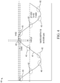
- FIG. 7 shows a graph 700 with a curve 701 showing a sinusoidal waveform of one of the AC input phases at the fundamental frequency of the AC power input feed (e.g., 60 Hz or 50 Hz), and a curve 702 showing a triangular modulating signal.
- FIG. 7 also shows a graph 710 with a curve 711 showing a pulse width modulated switching control signal generated by the rectifier controller 606 to control the active rectifier transistors of the corresponding phase.
- the IGBT-based active rectifier 601 in FIG. 6 is a three phase six pulse rectifier that uses transistors (e.g., IGBTs, field effect transistors (FETs), etc.) instead of SCRs.
- the active rectifier transistors are driven using SPWM as shown in FIG. 7 .
- the rectifier controller 606 in one example compares a sinusoidal waveform (e.g., curve 701) for each corresponding AC input phase (e.g., A, B, C) at the fundamental frequency to a respective triangle carrier waveform (e.g., curve 702) of a higher frequency, where the sinusoidal modulated signals 701 for the respective phases are shifted 120 degrees from one another.
- the pulse width modulation can be implemented using electrical circuitry of the rectifier controller 606 (e.g., sine wave generators and comparators) or the sinusoidal PWM can be implemented digitally using a programmed processor of the rectifier controller 606.
- the comparison by the rectifier controller 606 generates a series of pulses (e.g., curve 711) for each respective phase that encode the fundamental frequency within the pulse train.
- the ratio of the sinusoidal waveform amplitude (e.g., the amplitude of the curve 701) to the triangular carrier waveform amplitude (e.g., the amplitude of the curve 702) is the modulation index (MI).
- the rectifier controller 606 in one example varies the modulation index to change the duty cycle of each active rectifier transistor to adjust the rectified DC output of the IGBT rectifier 601 in order to control the system power.
- the high frequency current pulses of the active rectifier 601 are integrated through the low pass filter 610 coupled between the active rectifier input and the AC power feed.
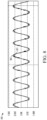
- a graph 800 in FIG. 8 includes a curve 801 showing AC input or line current for one example phase in the system 600, and a curve 802 showing the AC phase voltage of the corresponding AC input phase.
- the low pass filter 610 filters out the high switching frequency current of the active rectifier transistors and lets only the current of the fundamental frequency be reflected to the line. Since the current commutation is at a high frequency relative to the fundamental line frequency, the low pass filter 610 removes or significantly reduces the notches normally seen in the six-pulse rectification process, thereby reducing the THD in both the line voltage and line current. This resolves potential problems with equipment sharing the feed since the voltage distortion is very low eliminating multiple zero crossings.
- the rectifier controller 606 controls the relative phasing of the voltage and current waveforms to improve power factor as shown by the phase-aligned waveforms in the curves 801 and 802.
- the current e.g., curve 801
- the current can be held in phase with the voltage (curve 802) creating a displaced power factor equal to 1 (e.g., unity power factor).
- the rectifier controller 606 can vary the output voltage of the active rectifier 601 without affecting the displaced power factor as seen on the line.
- the CSI-based system 600 of FIG. 6 does not require a pony circuit or other starting circuitry since the inverter transistors (e.g., IGBTs) can be started without waiting for current to build in the parallel resonant tank to meet the minimum latching current of an SCR.
- the switches used in the inverter 603 are transistors which do not require a minimum latching current.
- the inverter 603 can simply be switched continuously.
- the inverter 603 is an H-bridge configuration with four IGBT transistors coupled between respective terminals of the DC link reactor and the parallel resonant tank circuit.
- FIG. 9 shows a graph 900 as a function of output current (amps RMS).
- the graph 900 has a curve 901 showing IGBT power (with respect to the Watts scale on the left of the figure), a curve 902 showing module watts, a curve 903 showing power of the diode of the inverter IGBT, as well as a curve 904 showing inverter IGBT junction temperature (with respect to the degrees C scale on the right of the figure), and a curve 905 showing the IGBT case temperature.
- the rectifier controller 606 holds the firing angle of the active rectifier 601 constant. This increases the loss in the inverter due to handling the required current at a high phase angle.
- the inverter IGBT module watt loss and junction temperature increase as phase angle is increased for the same amount of current.
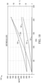
- FIG. 10 shows a graph 1000 as a function of output current (amps RMS) for an inverter phase angle held constant at 20 degrees.
- the graph 1000 has a curve 1001 showing IGBT power (with respect to the Watts scale on the left of the figure), a curve 1002 showing module watts, a curve 1003 showing power of the diode of the inverter IGBT, as well as a curve 1004 showing inverter IGBT junction temperature (with respect to the degrees C scale on the right of the figure), and a curve 1005 showing the IGBT case temperature.
- the rectifier controller 606 holds the firing angle of the active rectifier 601 constant. This increases the loss in the inverter 603 due to handling the required current at a high inverter phase angle. As shown in FIG. 10 , the current in the same module can be increased almost two times, which solves the de-rating problem.
- FIG. 11 shows an induction heating and melting VSI power system 1100 with a multiphase diode rectifier 1101, a DC link circuit 1102 with a DC link capacitor, an IGBT output inverter 1103, a series resonant tank circuit 1104 with an induction heating coil, and an inverter controller 1108.
- the voltage source inverter 1103 fed into the series resonant tank circuit 1104 provides advantages due to the ease of control, ease of impedance matching and reduced complexity, for example, without requiring any starting circuits.
- the rectifier 1101 is a multi-phase diode rectifier that converts the incoming AC to DC to provide a DC bus voltage across the DC link capacitor.
- the passive rectifier provides a generally constant line power factor, for example, .93 or better, but since the diodes cannot be turned on or off, the DC bus voltage output by the rectifier 1101 is constant for a constant AC input supply voltage, and the rectifier 1101 cannot be used to control the inverter output power.
- the output power can be controlled by frequency modulation of the inverter, for example, with the inverter controller 1108 generating signals to the inverter switches to turn on and off away from the resonant frequency of the series resonant tank circuit 1104.
- the inverter controller 1108 changes the frequency of the pulses to move toward the resonant frequency of the series resonant tank circuit 1104. As the frequency of the inverter switching control pulses gets closer to the natural resonant frequency of the series resonant tank circuit 1104, the output power of the inverter 1103 is increased.
- FIG. 12 includes a graph 1200 of inverter power and temperature in the system 1100 of FIG. 11 as a function of inverter phase angle.
- the graph 1200 has a curve 1201 showing IGBT power (with respect to the Watts scale on the left of the figure), a curve 1202 showing module watts, a curve 1203 showing power of the diode of the inverter IGBT, as well as a curve 1204 showing inverter IGBT junction temperature (with respect to the degrees C scale on the right of the figure), and a curve 1205 showing the IGBT case temperature.
- the module power loss curve 1202 also increases.
- FIG. 13 shows an induction heating and melting VSI power system 1300 according to another aspect.
- the system 1300 has an IGBT active rectifier and an IGBT inverter.
- the system 1300 includes a multiphase IGBT active rectifier 1301, a DC link circuit 1302 with a DC link reactor (e.g., choke), an IGBT output inverter 1303, a series resonant tank circuit 1304 including an induction heating coil, a rectifier controller 1306, an inverter controller 1308, and an input filter 1310.
- the inverter controller 1308 keeps the inverter phase angle fixed at a low value to reduce switching loss in the inverter switches. This allows the inverter current to be increased to trade switching loss for conduction loss and increase the output kw capability of the same inverter 1303.
- the active rectifier 1301 is a three phase six pulse active rectifier that uses transistors (e.g., IGBTs, FETs, etc.) instead of SCRs, and the rectifier controller 1306 drives the active rectifier transistors using SPWM (e.g., circuit-based or digital comparison of a sinusoidal waveform at the fundamental frequency of the AC input power to a triangle carrier waveform of a higher frequency as described above in connection with FIG. 7 ).
- SPWM e.g., circuit-based or digital comparison of a sinusoidal waveform at the fundamental frequency of the AC input power to a triangle carrier waveform of a higher frequency as described above in connection with FIG. 7 ).
- the rectifier controller 1306 in one example provides active rectifier switching control signals to the active rectifier 1301 having pulses that encode the fundamental frequency within the pulse train.
- the ratio of the sinusoidal waveform amplitude to the triangular carrier waveform amplitude is the modulation index, and the rectifier controller 1306 varies the modulation index to change the duty cycle of the active rectifier transistors to control the rectified DC output of the IGBT active rectifier 1301.
- the high frequency current pulses are integrated through the low pass filter 1310.
- the low pass filter 1310 filters out the high switching frequency current of the active rectifier transistors and lets only the current of the fundamental frequency to be reflected to the line.
- the inverter controller 1308 in one example holds (e.g., regulates) the inverter phase angle between the inverter output voltage and inverter output current at a fixed value, such as 15 degrees inductive, and the rectifier controller 1306 implements modulation index control to control the DC voltage feeding the inverter 1303 in order to control the output power of the inverter 1303. This reduces the inverter switching losses compared to the system 1100 of FIG. 11 and allows the inverter current to be increased without significantly increasing total inverter module losses.
Landscapes
- Physics & Mathematics (AREA)
- Electromagnetism (AREA)
- Engineering & Computer Science (AREA)
- Power Engineering (AREA)
- Inverter Devices (AREA)
- General Induction Heating (AREA)
- Rectifiers (AREA)
Claims (15)
- Leistungsumwandlungssystem (600; 1300), umfassend:einen aktiven Gleichrichter (601; 1301), der Gleichrichtertransistoren aufweist;einen Gleichstromzwischenkreis (602; 1302), der an einen Ausgang des aktiven Gleichrichters (601; 1301) gekoppelt ist;einen Umrichter (603; 1303), der Umrichtertransistoren und einen Eingang aufweist, der an den Gleichstromzwischenkreis (602; 1302) gekoppelt ist;eine Gleichrichter-Steuereinrichtung (606; 1306), die dazu ausgestaltet ist, die Gleichrichtertransistoren unter Verwendung von sinusförmiger Pulsbreitenmodulation (SPWM) mit Modulationsindex(MI)-Steuerung zu steuern;eine Umrichtersteuereinrichtung (608; 1308); undein Eingangsfilter (610; 1310), das an einen Eingang des aktiven Gleichrichters (601; 1301) gekoppelt ist; dadurch gekennzeichnet, dassein Resonanzschwingkreis (604; 1304) an einen Ausgang des Umrichters (603; 1303) gekoppelt ist, wobei der Resonanzschwingkreis (604; 1304) eine Induktionsheizspirale aufweist, unddie Gleichrichter-Steuereinrichtung (606; 1306) dazu ausgestaltet ist, die Gleichrichtertransistoren bei einem konstanten Winkel (α) zwischen dem Auslösen der Gleichrichtertransistoren in Bezug auf eine Wechselstrom-Eingangsphasenspannung zu steuern, um eine Systemausgangsleistung zu steuern.
- Leistungsumwandlungssystem (600) nach Anspruch 1, wobei der Gleichstromzwischenkreis (602) eine Gleichstromzwischenkreisdrossel aufweist, die an den Ausgang des aktiven Gleichrichters (601) gekoppelt ist.
- Leistungsumwandlungssystem (600) nach Anspruch 2, wobei die Umrichtersteuereinrichtung (608) dazu ausgestaltet ist, die Umrichtertransistoren zu steuern, um dem Resonanzschwingkreis (604) eine Umrichterausgangsspannung bei einer Umrichterausgangsfrequenz bereitzustellen, die höher ist als eine Resonanzfrequenz des Resonanzschwingkreises (604).
- Leistungsumwandlungssystem (600) nach Anspruch 2, wobei die Umrichtersteuereinrichtung (608) dazu ausgestaltet ist, die Umrichtertransistoren zu steuern, um dem Resonanzschwingkreis (604) eine Umrichterausgangsspannung bereitzustellen, und die Umrichtersteuereinrichtung (608) dazu ausgestaltet ist, einen Umrichterphasenwinkel zwischen der Umrichterausgangsspannung und einem Umrichterausgangsstrom auf einem festen Wert zu halten.
- Leistungsumwandlungssystem (600) nach Anspruch 2, wobei der Resonanzschwingkreis (604) ein Parallelschwingkreis ist.
- Leistungsumwandlungssystem (1300) nach Anspruch 1, wobei der Gleichstromzwischenkreis (1302) einen Gleichstromkondensator aufweist, der an den Ausgang des aktiven Gleichrichters (1301) gekoppelt ist.
- Leistungsumwandlungssystem (1300) nach Anspruch 6, wobei die Umrichtersteuereinrichtung (1308) dazu ausgestaltet ist, die Umrichtertransistoren zu steuern, um dem Resonanzschwingkreis (1304) eine Umrichterausgangsspannung mit einer Umrichterausgangsfrequenz bereitzustellen, die höher als eine Resonanzfrequenz des Resonanzschwingkreises (1304) ist.
- Leistungsumwandlungssystem (1300) nach Anspruch 6, wobei die Umrichtersteuereinrichtung (1308) dazu ausgestaltet ist, die Umrichtertransistoren zu steuern, um dem Resonanzschwingkreis (1304) eine Umrichterausgangsspannung bereitzustellen und die Umrichtersteuereinrichtung (1308) dazu ausgestaltet ist, einen Umrichterphasenwinkel zwischen der Umrichterausgangsspannung und einem Umrichterausgangsstrom auf einem festen Wert zu halten.
- Leistungsumwandlungssystem (1300) nach Anspruch 8, wobei die Umrichtersteuereinrichtung (1308) dazu ausgestaltet ist, den Umrichterphasenwinkel auf ungefähr 15 Grad zu steuern.
- Leistungsumwandlungssystem (1300) nach Anspruch 6, wobei der Resonanzschwingkreis (1304) ein Reihenschwingkreis ist.
- Leistungsumwandlungssystem nach Anspruch 1, wobei das System ein Stromquellenumrichtersystem ist, der Gleichstromzwischenkreis (602) eine Gleichstromzwischenkreisdrossel umfasst, die an den Ausgang des aktiven Gleichrichters (601) gekoppelt ist, und der Resonanzschwingkreis (604) ein Parallelschwingkreis ist.
- Leistungsumwandlungssystem nach Anspruch 1, wobei das System ein Spannungsquellenumrichtersystem ist, der Gleichstromzwischenkreis (602) einen Gleichstromzwischenkreiskondensator umfasst, der an den Ausgang des aktiven Gleichrichters (601) gekoppelt ist und der Resonanzschwingkreis (604) ein Reihenschwingkreis ist.
- Leistungsumwandlungssystem nach Anspruch 1, wobei die Umrichtersteuereinrichtung (1308) dazu ausgestaltet ist, die Umrichtertransistoren zu steuern, um dem Resonanzschwingkreis (1304) eine Umrichterausgangsspannung mit einer Umrichterausgangsfrequenz bereitzustellen, die höher als eine Resonanzfrequenz des Resonanzschwingkreises (1304) ist.
- Leistungsumwandlungssystem nach Anspruch 1, wobei die Umrichtersteuereinrichtung (1308) dazu ausgestaltet ist, die Umrichtertransistoren zu steuern, um dem Resonanzschwingkreis (1304) eine Umrichterausgangsspannung bereitzustellen und die Umrichtersteuereinrichtung (1308) dazu ausgestaltet ist, einen Umrichterphasenwinkel zwischen der Umrichterausgangsspannung und einem Umrichterausgangsstrom auf einem festen Wert zu halten.
- Leistungsumwandlungssystem nach Anspruch 14, wobei die Umrichtersteuereinrichtung (1308) dazu ausgestaltet ist, den Umrichterphasenwinkel auf ungefähr 15 Grad zu steuern.
Priority Applications (1)
| Application Number | Priority Date | Filing Date | Title |
|---|---|---|---|
| HRP20241565TT HRP20241565T1 (hr) | 2021-02-05 | 2022-01-28 | Aktivni ispravljač sa sustavima napajanja izmjenjivača izvora struje i izmjenjivača izvora napona za primjene u indukcijskom grijanju i taljenju |
Applications Claiming Priority (3)
| Application Number | Priority Date | Filing Date | Title |
|---|---|---|---|
| US202163146412P | 2021-02-05 | 2021-02-05 | |
| US202163271543P | 2021-10-25 | 2021-10-25 | |
| PCT/US2022/014310 WO2022169689A1 (en) | 2021-02-05 | 2022-01-28 | Active rectifier with current source inverter and voltage source inverter power systems for induction heating and melting applications |
Publications (4)
| Publication Number | Publication Date |
|---|---|
| EP4066596A1 EP4066596A1 (de) | 2022-10-05 |
| EP4066596A4 EP4066596A4 (de) | 2023-01-11 |
| EP4066596B1 true EP4066596B1 (de) | 2024-08-28 |
| EP4066596C0 EP4066596C0 (de) | 2024-08-28 |
Family
ID=82156688
Family Applications (1)
| Application Number | Title | Priority Date | Filing Date |
|---|---|---|---|
| EP22723536.3A Active EP4066596B1 (de) | 2021-02-05 | 2022-01-28 | Aktiver gleichrichter mit stromquellenumrichter- und spannungsquellenumrichter-leistungssystemen für induktionsheizung und schmelzanwendungen |
Country Status (9)
| Country | Link |
|---|---|
| US (1) | US20240172335A1 (de) |
| EP (1) | EP4066596B1 (de) |
| JP (1) | JP2024509642A (de) |
| ES (1) | ES2995286T3 (de) |
| HR (1) | HRP20241565T1 (de) |
| HU (1) | HUE069059T2 (de) |
| MX (1) | MX2023009257A (de) |
| PL (1) | PL4066596T3 (de) |
| WO (1) | WO2022169689A1 (de) |
Families Citing this family (1)
| Publication number | Priority date | Publication date | Assignee | Title |
|---|---|---|---|---|
| EP4344863A1 (de) | 2022-09-30 | 2024-04-03 | Essilor International | Herstellungsverfahren eines optischen artikels mit optischen elementen durch tintenstrahldruck |
Family Cites Families (23)
| Publication number | Priority date | Publication date | Assignee | Title |
|---|---|---|---|---|
| DE3220142C2 (de) * | 1982-05-28 | 1984-04-26 | Aeg-Elotherm Gmbh, 5630 Remscheid | Einrichtung zur induktiven Erwärmung von Werkstücken, insbesondere Rohren oder Stangen, mit mehreren Induktoren |
| US6366483B1 (en) * | 2000-07-24 | 2002-04-02 | Rockwell Automation Technologies, Inc. | PWM rectifier having de-coupled power factor and output current control loops |
| DE10110375B4 (de) * | 2001-03-03 | 2009-07-30 | Abp Induction Systems Gmbh | Induktionserwärmungsanlage |
| US7582851B2 (en) * | 2005-06-01 | 2009-09-01 | Inductotherm Corp. | Gradient induction heating of a workpiece |
| JP2007159175A (ja) * | 2005-11-30 | 2007-06-21 | Denki Kogyo Co Ltd | 電流型インバータ装置およびその制御方法 |
| ES2348506T3 (es) * | 2006-02-02 | 2010-12-07 | Panasonic Corporation | Aparato de calentamiento por inducción. |
| CN201238406Y (zh) * | 2008-06-27 | 2009-05-13 | 武汉理工大学 | 一种大功率节能电磁灶智能控制装置 |
| JP4506891B2 (ja) * | 2008-12-23 | 2010-07-21 | ダイキン工業株式会社 | 電流形電力変換回路 |
| JP5354652B2 (ja) * | 2009-01-13 | 2013-11-27 | 北芝電機株式会社 | 誘導加熱用電源装置 |
| JP5586872B2 (ja) * | 2009-05-07 | 2014-09-10 | 電気興業株式会社 | 三相単相直接電力変換器回路 |
| JP5708988B2 (ja) * | 2010-03-30 | 2015-04-30 | 株式会社ダイヘン | 高周波電源装置 |
| JP5267522B2 (ja) * | 2010-08-06 | 2013-08-21 | ダイキン工業株式会社 | 電力変換装置 |
| US8810182B2 (en) * | 2010-09-30 | 2014-08-19 | Rockwell Automation Technologies, Inc. | Adaptive harmonic reduction apparatus and methods |
| JP2012178944A (ja) * | 2011-02-28 | 2012-09-13 | Sanyo Electric Co Ltd | 電力変換装置、電力変換システム、およびモータインバータ |
| KR101308411B1 (ko) * | 2012-04-04 | 2013-09-13 | 전남대학교산학협력단 | 고속 공진점 추종방법 및 그 방법을 이용한 유도가열시스템 |
| KR102009512B1 (ko) * | 2015-04-14 | 2019-08-13 | 엘에스산전 주식회사 | 3상 인버터의 옵셋 전압 생성 장치 및 방법 |
| JP6552388B2 (ja) * | 2015-11-11 | 2019-07-31 | Mywayプラス株式会社 | 電流形電力変換装置の制御装置及び制御方法 |
| JP6596323B2 (ja) * | 2015-12-18 | 2019-10-23 | 三菱重工業株式会社 | コンバータ装置、駆動制御装置、モータ、およびコンプレッサ |
| KR101994572B1 (ko) * | 2016-05-24 | 2019-06-28 | 닛폰세이테츠 가부시키가이샤 | 전원 시스템 |
| GB2551824A (en) * | 2016-06-30 | 2018-01-03 | Univ Nottingham | High frequency high power converter system |
| WO2019147323A1 (en) * | 2018-01-26 | 2019-08-01 | Ajax Tocco Magnethermic Corporation | Wind turbine power conversion system and method |
| CN108767951A (zh) * | 2018-06-01 | 2018-11-06 | 薛洛良 | 一种用于电动车蓄电池的直流充电系统 |
| CN109068428A (zh) * | 2018-08-13 | 2018-12-21 | 中山市雅乐思商住电器有限公司 | 一种炊具、电力控制系统及方法 |
-
2022
- 2022-01-28 WO PCT/US2022/014310 patent/WO2022169689A1/en not_active Ceased
- 2022-01-28 PL PL22723536.3T patent/PL4066596T3/pl unknown
- 2022-01-28 US US17/779,156 patent/US20240172335A1/en active Pending
- 2022-01-28 JP JP2023560949A patent/JP2024509642A/ja active Pending
- 2022-01-28 HU HUE22723536A patent/HUE069059T2/hu unknown
- 2022-01-28 ES ES22723536T patent/ES2995286T3/es active Active
- 2022-01-28 MX MX2023009257A patent/MX2023009257A/es unknown
- 2022-01-28 EP EP22723536.3A patent/EP4066596B1/de active Active
- 2022-01-28 HR HRP20241565TT patent/HRP20241565T1/hr unknown
Also Published As
| Publication number | Publication date |
|---|---|
| EP4066596A1 (de) | 2022-10-05 |
| JP2024509642A (ja) | 2024-03-04 |
| US20240172335A1 (en) | 2024-05-23 |
| HUE069059T2 (hu) | 2025-02-28 |
| PL4066596T3 (pl) | 2025-01-07 |
| HRP20241565T1 (hr) | 2025-01-17 |
| EP4066596C0 (de) | 2024-08-28 |
| ES2995286T3 (en) | 2025-02-10 |
| MX2023009257A (es) | 2023-10-16 |
| EP4066596A4 (de) | 2023-01-11 |
| WO2022169689A1 (en) | 2022-08-11 |
Similar Documents
| Publication | Publication Date | Title |
|---|---|---|
| JP7051886B2 (ja) | Dcリンク電流リップルを低減するための駆動システムおよびその動作方法 | |
| EP3349343B1 (de) | Widerstandslose vorladung | |
| EP0344243B1 (de) | Verfahren und vorrichtung zur statischen quasiresonanzstromartleistungsumwandlung | |
| EP0292512B1 (de) | Statisches kraftumwandlungsverfahren und vorrichtung | |
| Mishima et al. | A bridgeless BHB ZVS-PWM AC–AC converter for high-frequency induction heating applications | |
| US20060103341A1 (en) | Bidirectional buck-boost power converters, electric starter generator system employing bidirectional buck-boost power converters, and methods therefor | |
| CN110739861B (zh) | 高频串联交流调压器 | |
| Edpuganti et al. | Optimal low switching frequency pulsewidth modulation of nine-level cascade inverter | |
| US7834597B1 (en) | System and method for AC voltage regulation | |
| CN109964537A (zh) | 高频率高功率转换器系统 | |
| JP2005033986A (ja) | 電圧制御パルス幅変調周波数変換器及びその制御方法 | |
| US20240172335A1 (en) | Active rectifier with current source inverter and voltage source inverter power systems for induction heating and melting applications | |
| Vodovozov et al. | Power electronic converters | |
| CA3161681C (en) | Active rectifier with current source inverter and voltage source inverter power systems for induction heating and melting applications | |
| CA3161681A1 (en) | Active rectifier with current source inverter and voltage source inverter power systems for induction heating and melting applications | |
| Ishikawa et al. | A novel soft-switched PWM current source inverter with voltage clamped circuit | |
| US12308762B2 (en) | Controller for power converter | |
| KR102269005B1 (ko) | 발전기 시스템 | |
| Konishi et al. | A novel time-sharing current-fed ZCS high frequency inverter-applied resonant dc-dc converter for inductive power transfer | |
| Keesara et al. | Design and development of three-phase high-frequency ac power distribution architecture for space application | |
| Reznikov et al. | Power semiconductor switches for pulse power transformers with a modular and scalable architecture | |
| EP4482003A1 (de) | Anordnung zur stromteilung von parallel geschalteten wandlern | |
| WO2025064558A1 (en) | Flyback converter with improved response | |
| Pravin et al. | Resonant Switched Capacitor Converter Based Multilevel Medium Voltage Drive for Voltage Balancing | |
| Kharadi et al. | Design Analysis and Simulation of Resonant Inverter for Induction Heating Process |
Legal Events
| Date | Code | Title | Description |
|---|---|---|---|
| STAA | Information on the status of an ep patent application or granted ep patent |
Free format text: STATUS: UNKNOWN |
|
| STAA | Information on the status of an ep patent application or granted ep patent |
Free format text: STATUS: THE INTERNATIONAL PUBLICATION HAS BEEN MADE |
|
| PUAI | Public reference made under article 153(3) epc to a published international application that has entered the european phase |
Free format text: ORIGINAL CODE: 0009012 |
|
| STAA | Information on the status of an ep patent application or granted ep patent |
Free format text: STATUS: REQUEST FOR EXAMINATION WAS MADE |
|
| 17P | Request for examination filed |
Effective date: 20220525 |
|
| AK | Designated contracting states |
Kind code of ref document: A1 Designated state(s): AL AT BE BG CH CY CZ DE DK EE ES FI FR GB GR HR HU IE IS IT LI LT LU LV MC MK MT NL NO PL PT RO RS SE SI SK SM TR |
|
| A4 | Supplementary search report drawn up and despatched |
Effective date: 20221208 |
|
| RIC1 | Information provided on ipc code assigned before grant |
Ipc: H05B 6/48 20060101ALI20221202BHEP Ipc: H05B 6/08 20060101ALI20221202BHEP Ipc: H05B 6/06 20060101ALI20221202BHEP Ipc: H05B 6/02 20060101AFI20221202BHEP |
|
| P01 | Opt-out of the competence of the unified patent court (upc) registered |
Effective date: 20230517 |
|
| STAA | Information on the status of an ep patent application or granted ep patent |
Free format text: STATUS: EXAMINATION IS IN PROGRESS |
|
| 17Q | First examination report despatched |
Effective date: 20230922 |
|
| REG | Reference to a national code |
Ref country code: DE Ref legal event code: R079 Free format text: PREVIOUS MAIN CLASS: H05B0006020000 Ipc: H05B0006040000 Ref document number: 602022005727 Country of ref document: DE |
|
| GRAP | Despatch of communication of intention to grant a patent |
Free format text: ORIGINAL CODE: EPIDOSNIGR1 |
|
| STAA | Information on the status of an ep patent application or granted ep patent |
Free format text: STATUS: GRANT OF PATENT IS INTENDED |
|
| INTG | Intention to grant announced |
Effective date: 20240318 |
|
| RIC1 | Information provided on ipc code assigned before grant |
Ipc: H05B 6/04 20060101AFI20240301BHEP |
|
| DAV | Request for validation of the european patent (deleted) | ||
| DAX | Request for extension of the european patent (deleted) | ||
| GRAS | Grant fee paid |
Free format text: ORIGINAL CODE: EPIDOSNIGR3 |
|
| GRAA | (expected) grant |
Free format text: ORIGINAL CODE: 0009210 |
|
| STAA | Information on the status of an ep patent application or granted ep patent |
Free format text: STATUS: THE PATENT HAS BEEN GRANTED |
|
| AK | Designated contracting states |
Kind code of ref document: B1 Designated state(s): AL AT BE BG CH CY CZ DE DK EE ES FI FR GB GR HR HU IE IS IT LI LT LU LV MC MK MT NL NO PL PT RO RS SE SI SK SM TR |
|
| REG | Reference to a national code |
Ref country code: CH Ref legal event code: EP |
|
| REG | Reference to a national code |
Ref country code: DE Ref legal event code: R096 Ref document number: 602022005727 Country of ref document: DE |
|
| REG | Reference to a national code |
Ref country code: IE Ref legal event code: FG4D |
|
| U01 | Request for unitary effect filed |
Effective date: 20240927 |
|
| P04 | Withdrawal of opt-out of the competence of the unified patent court (upc) registered |
Free format text: CASE NUMBER: APP_57814/2024 Effective date: 20241022 |
|
| U07 | Unitary effect registered |
Designated state(s): AT BE BG DE DK EE FI FR IT LT LU LV MT NL PT RO SE SI Effective date: 20241025 |
|
| REG | Reference to a national code |
Ref country code: GR Ref legal event code: EP Ref document number: 20240402718 Country of ref document: GR Effective date: 20241209 |
|
| REG | Reference to a national code |
Ref country code: SK Ref legal event code: T3 Ref document number: E 45354 Country of ref document: SK |
|
| REG | Reference to a national code |
Ref country code: HR Ref legal event code: T1PR Ref document number: P20241565 Country of ref document: HR |
|
| U20 | Renewal fee for the european patent with unitary effect paid |
Year of fee payment: 4 Effective date: 20241218 |
|
| PG25 | Lapsed in a contracting state [announced via postgrant information from national office to epo] |
Ref country code: IS Free format text: LAPSE BECAUSE OF FAILURE TO SUBMIT A TRANSLATION OF THE DESCRIPTION OR TO PAY THE FEE WITHIN THE PRESCRIBED TIME-LIMIT Effective date: 20241228 |
|
| PGFP | Annual fee paid to national office [announced via postgrant information from national office to epo] |
Ref country code: HR Payment date: 20241230 Year of fee payment: 4 |
|
| PG25 | Lapsed in a contracting state [announced via postgrant information from national office to epo] |
Ref country code: RS Free format text: LAPSE BECAUSE OF FAILURE TO SUBMIT A TRANSLATION OF THE DESCRIPTION OR TO PAY THE FEE WITHIN THE PRESCRIBED TIME-LIMIT Effective date: 20241128 |
|
| PG25 | Lapsed in a contracting state [announced via postgrant information from national office to epo] |
Ref country code: RS Free format text: LAPSE BECAUSE OF FAILURE TO SUBMIT A TRANSLATION OF THE DESCRIPTION OR TO PAY THE FEE WITHIN THE PRESCRIBED TIME-LIMIT Effective date: 20241128 Ref country code: IS Free format text: LAPSE BECAUSE OF FAILURE TO SUBMIT A TRANSLATION OF THE DESCRIPTION OR TO PAY THE FEE WITHIN THE PRESCRIBED TIME-LIMIT Effective date: 20241228 |
|
| REG | Reference to a national code |
Ref country code: HR Ref legal event code: ODRP Ref document number: P20241565 Country of ref document: HR Payment date: 20241230 Year of fee payment: 4 |
|
| REG | Reference to a national code |
Ref country code: ES Ref legal event code: FG2A Ref document number: 2995286 Country of ref document: ES Kind code of ref document: T3 Effective date: 20250210 |
|
| REG | Reference to a national code |
Ref country code: HU Ref legal event code: AG4A Ref document number: E069059 Country of ref document: HU |
|
| PG25 | Lapsed in a contracting state [announced via postgrant information from national office to epo] |
Ref country code: SM Free format text: LAPSE BECAUSE OF FAILURE TO SUBMIT A TRANSLATION OF THE DESCRIPTION OR TO PAY THE FEE WITHIN THE PRESCRIBED TIME-LIMIT Effective date: 20240828 |
|
| PG25 | Lapsed in a contracting state [announced via postgrant information from national office to epo] |
Ref country code: CZ Free format text: LAPSE BECAUSE OF FAILURE TO SUBMIT A TRANSLATION OF THE DESCRIPTION OR TO PAY THE FEE WITHIN THE PRESCRIBED TIME-LIMIT Effective date: 20240828 |
|
| PLBE | No opposition filed within time limit |
Free format text: ORIGINAL CODE: 0009261 |
|
| STAA | Information on the status of an ep patent application or granted ep patent |
Free format text: STATUS: NO OPPOSITION FILED WITHIN TIME LIMIT |
|
| 26N | No opposition filed |
Effective date: 20250530 |
|
| REG | Reference to a national code |
Ref country code: CH Ref legal event code: PL |
|
| PG25 | Lapsed in a contracting state [announced via postgrant information from national office to epo] |
Ref country code: MC Free format text: LAPSE BECAUSE OF FAILURE TO SUBMIT A TRANSLATION OF THE DESCRIPTION OR TO PAY THE FEE WITHIN THE PRESCRIBED TIME-LIMIT Effective date: 20240828 |
|
| PG25 | Lapsed in a contracting state [announced via postgrant information from national office to epo] |
Ref country code: CH Free format text: LAPSE BECAUSE OF NON-PAYMENT OF DUE FEES Effective date: 20250131 |
|
| PGFP | Annual fee paid to national office [announced via postgrant information from national office to epo] |
Ref country code: GB Payment date: 20251211 Year of fee payment: 5 |
|
| PGFP | Annual fee paid to national office [announced via postgrant information from national office to epo] |
Ref country code: NO Payment date: 20251216 Year of fee payment: 5 |
|
| PGFP | Annual fee paid to national office [announced via postgrant information from national office to epo] |
Ref country code: GR Payment date: 20251230 Year of fee payment: 5 |
|
| PGFP | Annual fee paid to national office [announced via postgrant information from national office to epo] |
Ref country code: IE Payment date: 20251204 Year of fee payment: 5 |
|
| U20 | Renewal fee for the european patent with unitary effect paid |
Year of fee payment: 5 Effective date: 20251217 |
|
| PGFP | Annual fee paid to national office [announced via postgrant information from national office to epo] |
Ref country code: PL Payment date: 20251218 Year of fee payment: 5 |
|
| PGFP | Annual fee paid to national office [announced via postgrant information from national office to epo] |
Ref country code: SK Payment date: 20251216 Year of fee payment: 5 |
|
| PGFP | Annual fee paid to national office [announced via postgrant information from national office to epo] |
Ref country code: HU Payment date: 20260113 Year of fee payment: 5 |
|
| PGFP | Annual fee paid to national office [announced via postgrant information from national office to epo] |
Ref country code: ES Payment date: 20260205 Year of fee payment: 5 |