EP4064483B1 - Structure de douille - Google Patents
Structure de douille Download PDFInfo
- Publication number
- EP4064483B1 EP4064483B1 EP21198814.2A EP21198814A EP4064483B1 EP 4064483 B1 EP4064483 B1 EP 4064483B1 EP 21198814 A EP21198814 A EP 21198814A EP 4064483 B1 EP4064483 B1 EP 4064483B1
- Authority
- EP
- European Patent Office
- Prior art keywords
- socket structure
- plate
- extending portion
- frame
- lateral walls
- Prior art date
- Legal status (The legal status is an assumption and is not a legal conclusion. Google has not performed a legal analysis and makes no representation as to the accuracy of the status listed.)
- Active
Links
Images


Classifications
-
- H—ELECTRICITY
- H01—ELECTRIC ELEMENTS
- H01R—ELECTRICALLY-CONDUCTIVE CONNECTIONS; STRUCTURAL ASSOCIATIONS OF A PLURALITY OF MUTUALLY-INSULATED ELECTRICAL CONNECTING ELEMENTS; COUPLING DEVICES; CURRENT COLLECTORS
- H01R13/00—Details of coupling devices of the kinds covered by groups H01R12/70 or H01R24/00 - H01R33/00
- H01R13/46—Bases; Cases
- H01R13/502—Bases; Cases composed of different pieces
-
- H—ELECTRICITY
- H01—ELECTRIC ELEMENTS
- H01R—ELECTRICALLY-CONDUCTIVE CONNECTIONS; STRUCTURAL ASSOCIATIONS OF A PLURALITY OF MUTUALLY-INSULATED ELECTRICAL CONNECTING ELEMENTS; COUPLING DEVICES; CURRENT COLLECTORS
- H01R24/00—Two-part coupling devices, or either of their cooperating parts, characterised by their overall structure
- H01R24/76—Two-part coupling devices, or either of their cooperating parts, characterised by their overall structure with sockets, clips or analogous contacts and secured to apparatus or structure, e.g. to a wall
-
- H—ELECTRICITY
- H01—ELECTRIC ELEMENTS
- H01R—ELECTRICALLY-CONDUCTIVE CONNECTIONS; STRUCTURAL ASSOCIATIONS OF A PLURALITY OF MUTUALLY-INSULATED ELECTRICAL CONNECTING ELEMENTS; COUPLING DEVICES; CURRENT COLLECTORS
- H01R13/00—Details of coupling devices of the kinds covered by groups H01R12/70 or H01R24/00 - H01R33/00
- H01R13/46—Bases; Cases
-
- H—ELECTRICITY
- H01—ELECTRIC ELEMENTS
- H01R—ELECTRICALLY-CONDUCTIVE CONNECTIONS; STRUCTURAL ASSOCIATIONS OF A PLURALITY OF MUTUALLY-INSULATED ELECTRICAL CONNECTING ELEMENTS; COUPLING DEVICES; CURRENT COLLECTORS
- H01R12/00—Structural associations of a plurality of mutually-insulated electrical connecting elements, specially adapted for printed circuits, e.g. printed circuit boards [PCB], flat or ribbon cables, or like generally planar structures, e.g. terminal strips, terminal blocks; Coupling devices specially adapted for printed circuits, flat or ribbon cables, or like generally planar structures; Terminals specially adapted for contact with, or insertion into, printed circuits, flat or ribbon cables, or like generally planar structures
- H01R12/70—Coupling devices
- H01R12/71—Coupling devices for rigid printing circuits or like structures
- H01R12/712—Coupling devices for rigid printing circuits or like structures co-operating with the surface of the printed circuit or with a coupling device exclusively provided on the surface of the printed circuit
- H01R12/716—Coupling device provided on the PCB
-
- H—ELECTRICITY
- H01—ELECTRIC ELEMENTS
- H01R—ELECTRICALLY-CONDUCTIVE CONNECTIONS; STRUCTURAL ASSOCIATIONS OF A PLURALITY OF MUTUALLY-INSULATED ELECTRICAL CONNECTING ELEMENTS; COUPLING DEVICES; CURRENT COLLECTORS
- H01R13/00—Details of coupling devices of the kinds covered by groups H01R12/70 or H01R24/00 - H01R33/00
- H01R13/66—Structural association with built-in electrical component
- H01R13/665—Structural association with built-in electrical component with built-in electronic circuit
- H01R13/6658—Structural association with built-in electrical component with built-in electronic circuit on printed circuit board
-
- H—ELECTRICITY
- H02—GENERATION; CONVERSION OR DISTRIBUTION OF ELECTRIC POWER
- H02G—INSTALLATION OF ELECTRIC CABLES OR LINES, OR OF COMBINED OPTICAL AND ELECTRIC CABLES OR LINES
- H02G3/00—Installations of electric cables or lines or protective tubing therefor in or on buildings, equivalent structures or vehicles
- H02G3/02—Details
- H02G3/08—Distribution boxes; Connection or junction boxes
- H02G3/18—Distribution boxes; Connection or junction boxes providing line outlets
-
- H—ELECTRICITY
- H02—GENERATION; CONVERSION OR DISTRIBUTION OF ELECTRIC POWER
- H02G—INSTALLATION OF ELECTRIC CABLES OR LINES, OR OF COMBINED OPTICAL AND ELECTRIC CABLES OR LINES
- H02G3/00—Installations of electric cables or lines or protective tubing therefor in or on buildings, equivalent structures or vehicles
- H02G3/02—Details
- H02G3/08—Distribution boxes; Connection or junction boxes
- H02G3/081—Bases, casings or covers
Definitions
- the present disclosure relates to a socket structure, and more particularly to a socket structure that a metallic frame and a casing thereof are combined with each other.
- Power socket is an essential product for modern life as an electric power supply.
- USB connectors are commonly used transmission interfaces for charging the electronic devices. Therefore, it became a growing trend of setting USB ports on power sockets.
- the requirement of power increases.
- the limitation of arrangements and sizes of the components inside the power sockets local overheating frequently occurs to the power sockets with USB ports. Since the component damage owing to the overheating should be avoided, it is still hard to increase the total wattage carried by the power sockets with USB ports.
- EP 3 189 567 B1 relates to a connection unit suitable for mounting in a mounting volume of a predetermined size of a building, comprising: a housing intended to receive at least some of the functional elements of the connection unit and designed as a housing pot having a pot opening, a peripheral pot side wall and a pot base, and a mounting frame having a substantially planar base plate by means of which the connection unit can be attached to a surface of the building, the housing pot comprising a housing main part and a housing cover part which can be interconnected, the line of separation between the housing main part and the housing cover part extending from a first edge portion of the pot opening, through a first portion of the pot side wall, then through the pot base and then further through a second portion of the pot side wall and ending in a second edge portion of the pot opening. At least one pair of guide rails which extend substantially orthogonally to the line of separation are provided on the housing main part for guiding a printed circuit board or a plurality of printed circuit boards of an electronic assembly of the connection unit.
- EP 3 605 749 A1 discloses an appliance support comprising a frame provided with fastener means for fastening to an electrical box, the frame presenting an inner edge that defines a mounting opening for mounting an appliance mechanism, the inner edge being extended rearwards by a side wall that defines a housing for receiving said appliance mechanism, said housing being closed at the back by a back wall that completely closes said housing, wherein said back wall is arranged to receive at least three electrical connection terminals housed in three mutually insulated compartments, said compartments being defined by partitions made of insulating material and placed on an inside face of the back wall, wherein individual orifices are provided, each giving access from outside the housing directly to a respective one of said compartments for electrically powering the connection terminal housed in said compartment, said appliance support further comprising at least one insulating cover that is configured to be fitted in said housing and to enclose said connection terminals, and that includes individual openings each configured to give access via the mounting opening from the inside of the housing directly to a respective one of the compartments for insert
- the thermal conductivity of the socket structure is improved.
- the heat inside the socket structure can be efficiently conducted to the exterior of the socket structure to improve the heat dissipating effect, and the problem of local overheating can be obviated. It is beneficial to increase the total wattage carried by the socket structure and meet the requirement of high power in the market.
- the present invention relates to a socket structure according to independent claim 1.
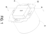
- FIG. 1 is a schematic perspective view illustrating the socket structure according to a first embodiment of the present invention.
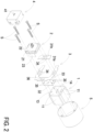
- FIG. 2 is an exploded view illustrating the socket structure of FIG. 1 .
- FIG. 3 is a cross-sectional view illustrating the socket structure along the section line A-A' of FIG. 1 .
- the socket structure includes a casing 1, a main body 2, a frame 3 and a cover 4.
- the casing 1 includes plural lateral walls 11, a bottom 12, an opening 13 and an accommodation space 14.
- the opening 13 is collaboratively defined by the lateral walls 11.
- the accommodation space 14 is collaboratively defined by the lateral walls 11 and the bottom 12 and is in communication with the opening 13.
- the main body 2 is disposed in the accommodation space 14 and includes a circuit board 21 and a connection port 22.
- the connection port 22 is disposed on the circuit board 21.
- the frame 3 includes at least one plate 31 and a first extending portion 32.
- the plate 31 surrounds the periphery of the opening 13.
- the first extending portion 32 is extended from the plate 31 and is connected to one of the lateral walls 11.
- the cover 4 covers the opening 13 and includes a through hole 41.
- the through hole 41 is configured to allow a plug (not shown) to pass through and connect to the connection port 22.
- the plug is a USB plug
- the connection port 22 is a USB port.
- the frame 3 is preferably but not exclusively made of metal, thereby improving the thermal conductivity of the socket structure. Consequently, the heat inside the socket structure can be conducted to the exterior, and thus the problem of local overheating is addressed.
- the casing 1 has a cube profile. That is, the casing 1 includes four lateral walls 11, and the opening 13 defined by the lateral walls 11 also has a square profile. In this embodiment, the thicknesses of the lateral walls 11 and the bottom 12 are ranged between 1.0 mm and 3.0 mm, but not limited thereto.
- the cover 4 is connected to the inner surfaces of the four lateral walls 11, so as to cover and seal the opening 13.
- the frame 3 is preferably but not exclusively made of a metallic plate, and a thickness of the metallic plate is ranged between 0.5 mm and 2.0 mm.
- the frame 3 includes a first plate 31a and a second plate 31b.
- the first plate 31a has a U-shaped profile and includes three inner edges.
- the first plate 31a and the second plate 31b collaboratively surrounds the periphery of the opening 13, but not limited thereto.
- the first plate 31a and the second plate 31b are integrally formed.
- the first extending portion 32 is extended from one of the inner edges of the first plate 31a.
- the first extending portion 32 is extended from the inner edge of the first plate 31a which is opposite to the second plate 31b.
- the frame 3 further includes a second extending portion 33.
- the second extending portion 33 is connected to the first extending portion 32, and the first extending portion 32 and the second extending portion 33 collaboratively form an L-shaped structure.
- the first extending portion 32 and the second extending portion 33 can be integrally formed by bending the metallic plate, but not limited thereto.
- the first extending portion 32 and the second extending portion 33 are respectively embedded in one of the lateral walls 11 and the bottom 12 of the casing 1 by an insert molding process.
- the frame 3 further includes a plurality of positioning holes 35.
- the positioning holes 35 are formed on the first extending portion 32 and the second extending portion 33, so that the material of the casing 1 can flow through the positioning holes 35 during the insert molding process. It is beneficial to position the first extending portion 32 and the second extending portion 33 inside the casing 1.
- a diameter of each of the positioning holes 35 is ranged between 0.5 mm and 1.0 mm, but not limited thereto.
- the frame 3 further includes a plurality of third extending portions 34.
- the third extending portions 34 are extended from the first plate 31a and the second plate 31b and are connected to the lateral walls 11 of the casing 1.
- the third extending portions 34 are preferably but not exclusively embedded in the lateral walls 11 by the insert molding process, so that the frame 3 is firmly combined and fixed with the casing 1.
- the frame 3 includes six third extending portions 34, but not limited thereto.
- Four of the third extending portions 34 are disposed on the first plate 31a. More specifically, two of the third extending portions 34 are disposed on each of the inner edges of the first plate 31a except the inner edge where the first extending portion 32 is extended from. Two of the third extending portions 34 are disposed on the second plate 31b.
- FIG. 4 is an exploded view illustrating the socket structure according to a second embodiment of the present disclosure, which is not covered by the subject-matter of the claims.
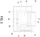
- FIG. 5 is a cross-sectional view illustrating the socket structure of FIG. 4 .
- the main difference between the first embodiment and the second embodiment is the combination way of the frame 3' and the casing 1. Therefore, the similar structures of the main body 2 and the cover 4 are not redundantly described here.
- the first extending portion 32' and the second extending portion 33' are respectively attached on outer surfaces of one of the lateral walls 11 and the bottom 12.
- the third extending portions 34 are embedded in the lateral walls 11, but not limited thereto.
- the third extending portions 34 are attached on the outer surfaces of the lateral walls 11.
- the positioning holes 35 is only formed on the second extending portion 33', but not limited thereto.
- the socket structure further includes an insulating covering 5.
- the insulating covering 5 covers and accommodates the lateral walls 11, the bottom 12, the first extending portion 32' and the second extending portion 33', so as to achieve the insulating effect.
- the socket structure further includes four fixing components S.
- the frame 3' further includes four fixing grooves 36.
- the fixing grooves 36 are formed on the first plate 31a and the second plate 31b.
- the fixing components S pass through the fixing grooves 36 and are connected to the insulating covering 5, so that the frame 3' and the casing 1 are combined and fixed with the insulating covering 5.
- the socket structure further includes a glue layer (not shown).
- the glue layer is filled between the bottom 12 of the casing 1 and the lower surface of the circuit board 21 of the main body 2, so that the thermal conductivity of the socket structure is further improved.
- the main body 2 further includes a heat conducting component 23.
- the heat conducting component 23 is preferably but not exclusively a plate structure.
- the heat conducting component 23 is connected to the circuit board 21 and is extended from the circuit board 21 toward the bottom 12 of the casing 1. In other words, the extending direction of the heat conducting component 23 is parallel to the extending direction of the first extending portions 32, 32' of the frames 3, 3', but not limited thereto.
- the heat conducting component 23 is directly in contact with the first extending portions 32, 32'.
- the glue layer is filled between the heat conducting component 23 and the first extending portions 32, 32' of the frames 3, 3'.
- the present disclosure provides a socket structure.
- the frame and the casing are firmly combined with each other.
- the effect of heat dissipating of the socket structure is improved, and the problem of local overheating is avoided.
- the steps of installing the socket structure are reduced, and the assembly cost thereof is reduced accordingly.
Landscapes
- Engineering & Computer Science (AREA)
- Microelectronics & Electronic Packaging (AREA)
- Architecture (AREA)
- Civil Engineering (AREA)
- Structural Engineering (AREA)
- Coupling Device And Connection With Printed Circuit (AREA)
- Connector Housings Or Holding Contact Members (AREA)
Claims (9)
- Structure de prise, comprenant:un boîtier (1) comprenant une pluralité de parois latérales (11), un fond (12), une ouverture (13) et un espace d'accueil (14), dans lequel l'ouverture (13) est défini collaborativement par la pluralité de parois latérales (11), et l'espace d'accueil (14) est défini collaborativement par la pluralité de parois latérales (11) et le fond (12) et est en communication avec l'ouverture (13);un corps principal (2) disposé dans l'espace d'accueil (14) et comprenant une carte de circuit (21) et un port de connexion (22), dans lequel le port de connexion (22) est disposé sur la carte de circuit (21);un cadre (3) comprenant au moins une plaque (31) et une première partie étendue (32), dans laquelle l'au moins une plaque (31) entoure la périphérie de l'ouverture (13), et la première partie étendue (32) s'étend depuis l'au moins une plaque (31) et est connectée à une de la pluralité de parois latérales (11); etun couvercle (4) couvrant l'ouverture (13) et comprenant un trou de passage (41), dans laquelle le trou de passage (41) est configuré pour permettre à une prise de passer à travers et de se connecter au port de connexion (22), dans laquellele cadre (3) comprend en outre une seconde partie étendue (33), et la seconde partie étendue (33) est connectée à la première partie étendue (32) et connectée au fond (12) du boîtier (1), caractérisé en ce que la première partie étendue (32) et la seconde partie étendue (33) sont respectivement incorporées dans une de la pluralité de parois latérales (11) et le fond (12) du boîtier (1) par un procédé de moulage d'insert.
- Structure de prise selon la revendication 1, dans laquelle le cadre (3) comprend en outre une pluralité de trous de positionnement (35) formés sur au moins une de la première partie étendue (32) et la seconde partie étendue (33).
- Structure de prise selon la revendication 1, dans laquelle le cadre (3) comprend en outre une pluralité de troisièmes parties étendues (34), et la pluralité de troisièmes parties étendues (34) s'étendent depuis l'au moins une plaque (31) et sont connectées à la pluralité de parois latérales (11).
- Structure de prise selon la revendication 3, dans laquelle les troisièmes parties étendues (34) sont incorporées dans la pluralité de parois latérales (11) par un procédé de moulage d'insert.
- Structure de prise selon la revendication 1, dans laquelle le cadre (3) comprend une première plaque (31a) et une seconde plaque (31b), dans laquelle le première plaque (31a) a un profil en forme de U, la première plaque (31a) et la seconde plaque (31b) entourent collaborativement la périphérie de l'ouverture (13), et la première partie étendue (32) s'étend depuis un bord intérieur de la première plaque (31a).
- Structure de prise selon la revendication 1, dans laquelle la clé est une clé USB, et le port de connexion (22) est un port USB.
- Structure de prise selon la revendication 1, dans laquelle le cadre (3) est fait de métal.
- Structure de prise selon la revendication 1, comprenant en outre une couche de colle, dans laquelle la couche de colle est remplie entre le fond (12) du boîtier (1) et la carte de circuit (21) du corps principal (2).
- Structure de prise selon la revendication 1, dans laquelle le corps principal (2) comprend en outre un composant thermoconducteur (23), et le composant thermoconducteur (23) est connecté à la carte de circuit (21) et s'étend de la carte de circuit (21) jusqu'au fond (12) du boîtier (1).
Applications Claiming Priority (1)
| Application Number | Priority Date | Filing Date | Title |
|---|---|---|---|
| CN202110302580.XA CN115117670B (zh) | 2021-03-22 | 2021-03-22 | 插座结构 |
Publications (3)
| Publication Number | Publication Date |
|---|---|
| EP4064483A1 EP4064483A1 (fr) | 2022-09-28 |
| EP4064483B1 true EP4064483B1 (fr) | 2024-11-13 |
| EP4064483C0 EP4064483C0 (fr) | 2024-11-13 |
Family
ID=77951512
Family Applications (1)
| Application Number | Title | Priority Date | Filing Date |
|---|---|---|---|
| EP21198814.2A Active EP4064483B1 (fr) | 2021-03-22 | 2021-09-24 | Structure de douille |
Country Status (4)
| Country | Link |
|---|---|
| US (1) | US11637395B2 (fr) |
| EP (1) | EP4064483B1 (fr) |
| JP (1) | JP7225340B2 (fr) |
| CN (1) | CN115117670B (fr) |
Families Citing this family (3)
| Publication number | Priority date | Publication date | Assignee | Title |
|---|---|---|---|---|
| CN115117670B (zh) * | 2021-03-22 | 2025-11-11 | 台达电子工业股份有限公司 | 插座结构 |
| EP4456351A1 (fr) * | 2023-04-25 | 2024-10-30 | Albrecht Jung GmbH & Co. KG | Appareil électrique/électronique et procédé de dissipation de chaleur d'un appareil électrique/électronique |
| CN117039507B (zh) * | 2023-09-21 | 2026-02-24 | 佛山市顺德区曼邦电气实业有限公司 | 一种面散热式电连接器 |
Citations (1)
| Publication number | Priority date | Publication date | Assignee | Title |
|---|---|---|---|---|
| TW201225450A (en) * | 2010-12-10 | 2012-06-16 | Silitek Electronic Gz Co Ltd | Heat dissipation structure |
Family Cites Families (31)
| Publication number | Priority date | Publication date | Assignee | Title |
|---|---|---|---|---|
| US4149220A (en) * | 1976-02-19 | 1979-04-10 | Chrysler Corporation | Arrangement for mounting a transducer on a housing |
| JPS57195879U (fr) | 1981-06-05 | 1982-12-11 | ||
| US4485282A (en) * | 1983-01-28 | 1984-11-27 | Lee Long River | Plug-in type of safety wall switch and wall outlet |
| JPH0672182U (ja) | 1993-03-10 | 1994-10-07 | デルタ エレクトロニクス インコーポレイティド | 電源フィルタ |
| US5603622A (en) * | 1995-03-17 | 1997-02-18 | Taiwan King Prince Co., Ltd. | Track light mounting arrangement |
| WO1998002940A1 (fr) | 1996-07-12 | 1998-01-22 | Siemens Aktiengesellschaft | Connecteur femelle blinde de carte imprimee avec mise en contact de blindage avec la paroi d'un appareil |
| US6198631B1 (en) * | 1999-12-03 | 2001-03-06 | Pass & Seymour, Inc. | High temperature ground connection |
| JP2004165251A (ja) | 2002-11-11 | 2004-06-10 | Sharp Corp | 電子部品の放熱装置 |
| JP4200306B2 (ja) | 2002-11-18 | 2008-12-24 | パナソニック電工株式会社 | 配線器具 |
| TWI234173B (en) * | 2002-12-10 | 2005-06-11 | Delta Electronics Inc | Assembly structure of the adapter |
| JP2004234866A (ja) | 2003-01-28 | 2004-08-19 | Funai Electric Co Ltd | プリント基板装置およびそのコネクタソケット実装方法 |
| DE102004007180B4 (de) | 2003-02-14 | 2015-10-22 | Autonetworks Technologies, Ltd. | Verteilereinheit und elektrisches Verbindungsgehäuse hiermit |
| CN100388471C (zh) * | 2004-01-16 | 2008-05-14 | 华硕电脑股份有限公司 | 遮蔽模块 |
| US7234954B1 (en) | 2006-06-01 | 2007-06-26 | Srage Jay M | International electrical receptacle |
| FR2939272B1 (fr) | 2008-12-02 | 2011-03-18 | Legrand France | Plaque d'habillage pour appareillage electrique |
| TWI395541B (zh) * | 2009-12-01 | 2013-05-01 | Delta Electronics Inc | 插座端子散熱結構 |
| FR3000310B1 (fr) * | 2012-12-20 | 2014-12-26 | Legrand France | Module d'appareillage electrique |
| DE102014217481A1 (de) | 2014-09-02 | 2016-03-03 | Fränkische Rohrwerke Gebr. Kirchner Gmbh & Co. Kg | Anschlusseinheit |
| JP6800173B2 (ja) * | 2016-02-05 | 2020-12-16 | イリソ電子工業株式会社 | 撮像装置用部品及び撮像装置 |
| US10734773B2 (en) | 2016-04-18 | 2020-08-04 | Ingenio Aerospace Inc. | Infrastructure for mobile devices and electronic loose equipment |
| DE102017202303B3 (de) | 2017-02-14 | 2018-07-19 | Festo Ag & Co. Kg | Elektronikmodul für die industrielle Automatisierung und Verfahren zu seiner Herstellung |
| DE102017108638A1 (de) | 2017-04-24 | 2018-10-25 | Hirschmann Car Communication Gmbh | Abgesetztes Tunermodul mit verbesserten Wärmeeigenschaften |
| CN207442047U (zh) | 2017-09-28 | 2018-06-01 | 飞利富科技股份有限公司 | 双usb接口插座 |
| EP3462820B1 (fr) * | 2017-09-29 | 2021-08-04 | Hosiden Corporation | Boîtier de connecteur et procédé d'assemblage correspondant |
| CN207994259U (zh) | 2018-02-02 | 2018-10-19 | 广州雷神电气制造有限公司 | 墙壁电源插座 |
| FR3084781B1 (fr) | 2018-07-31 | 2021-05-14 | Legrand France | Support d’appareillage electrique et appareillage electrique associe |
| US10910743B2 (en) * | 2018-11-06 | 2021-02-02 | Lear Corporation | Electrical assembly and method |
| JP2021162957A (ja) | 2020-03-30 | 2021-10-11 | 本田技研工業株式会社 | 収容領域管理装置 |
| CN114498117B (zh) * | 2020-10-23 | 2024-06-18 | 台达电子工业股份有限公司 | 插座结构 |
| CN115117670B (zh) * | 2021-03-22 | 2025-11-11 | 台达电子工业股份有限公司 | 插座结构 |
| CN115313110B (zh) * | 2021-05-07 | 2025-06-24 | 台达电子工业股份有限公司 | 插头 |
-
2021
- 2021-03-22 CN CN202110302580.XA patent/CN115117670B/zh active Active
- 2021-07-27 US US17/443,669 patent/US11637395B2/en active Active
- 2021-09-24 EP EP21198814.2A patent/EP4064483B1/fr active Active
- 2021-10-01 JP JP2021162957A patent/JP7225340B2/ja active Active
Patent Citations (1)
| Publication number | Priority date | Publication date | Assignee | Title |
|---|---|---|---|---|
| TW201225450A (en) * | 2010-12-10 | 2012-06-16 | Silitek Electronic Gz Co Ltd | Heat dissipation structure |
Also Published As
| Publication number | Publication date |
|---|---|
| JP7225340B2 (ja) | 2023-02-20 |
| CN115117670B (zh) | 2025-11-11 |
| CN115117670A (zh) | 2022-09-27 |
| US20220302626A1 (en) | 2022-09-22 |
| EP4064483C0 (fr) | 2024-11-13 |
| JP2022146854A (ja) | 2022-10-05 |
| US11637395B2 (en) | 2023-04-25 |
| EP4064483A1 (fr) | 2022-09-28 |
Similar Documents
| Publication | Publication Date | Title |
|---|---|---|
| EP4064483B1 (fr) | Structure de douille | |
| US11411355B2 (en) | Electrical connector assembly | |
| CN204964818U (zh) | 插座组件及模块组件 | |
| US9343725B2 (en) | Bus bar module and power supply unit | |
| CN103001044B (zh) | 电连接器 | |
| CN109561611B (zh) | 具有隔热功能的电源供应器 | |
| US20050181642A1 (en) | Transmission module assembly having printed circuit board | |
| US12010804B2 (en) | Power receptacle | |
| US20230387632A1 (en) | Electrical connector | |
| EP2985839B1 (fr) | Fiche | |
| JP4619992B2 (ja) | 電気接続箱 | |
| TW201904370A (zh) | 電源轉換器及其電連接器模組 | |
| US7241174B2 (en) | Electrical connector with a metal housing | |
| TW201818439A (zh) | 開關接線裝置之模組化結構 | |
| JP4880492B2 (ja) | 電子装置のハウジング構造体及びハウジング構造体の形成方法 | |
| CN108232697B (zh) | 电连接器 | |
| EP1542521B1 (fr) | Dispositif électronique | |
| CN107666817B (zh) | 控制器组件、控制盒及风机 | |
| KR101794338B1 (ko) | 조인트 커넥터 | |
| JP7157179B2 (ja) | 配線器具 | |
| JP7157180B2 (ja) | 配線器具 | |
| JP4374297B2 (ja) | 電気接続箱及びその製造方法 | |
| CN220774806U (zh) | 排插结构 | |
| JP7555228B2 (ja) | 充電器 | |
| KR20140002707U (ko) | 커넥터 |
Legal Events
| Date | Code | Title | Description |
|---|---|---|---|
| PUAI | Public reference made under article 153(3) epc to a published international application that has entered the european phase |
Free format text: ORIGINAL CODE: 0009012 |
|
| STAA | Information on the status of an ep patent application or granted ep patent |
Free format text: STATUS: THE APPLICATION HAS BEEN PUBLISHED |
|
| AK | Designated contracting states |
Kind code of ref document: A1 Designated state(s): AL AT BE BG CH CY CZ DE DK EE ES FI FR GB GR HR HU IE IS IT LI LT LU LV MC MK MT NL NO PL PT RO RS SE SI SK SM TR |
|
| STAA | Information on the status of an ep patent application or granted ep patent |
Free format text: STATUS: REQUEST FOR EXAMINATION WAS MADE |
|
| 17P | Request for examination filed |
Effective date: 20221024 |
|
| RBV | Designated contracting states (corrected) |
Designated state(s): AL AT BE BG CH CY CZ DE DK EE ES FI FR GB GR HR HU IE IS IT LI LT LU LV MC MK MT NL NO PL PT RO RS SE SI SK SM TR |
|
| GRAP | Despatch of communication of intention to grant a patent |
Free format text: ORIGINAL CODE: EPIDOSNIGR1 |
|
| STAA | Information on the status of an ep patent application or granted ep patent |
Free format text: STATUS: GRANT OF PATENT IS INTENDED |
|
| RIC1 | Information provided on ipc code assigned before grant |
Ipc: H02G 3/08 20060101ALN20240513BHEP Ipc: H01R 24/76 20110101ALI20240513BHEP Ipc: H01R 13/66 20060101ALI20240513BHEP Ipc: H02G 3/18 20060101AFI20240513BHEP |
|
| INTG | Intention to grant announced |
Effective date: 20240606 |
|
| GRAS | Grant fee paid |
Free format text: ORIGINAL CODE: EPIDOSNIGR3 |
|
| GRAA | (expected) grant |
Free format text: ORIGINAL CODE: 0009210 |
|
| STAA | Information on the status of an ep patent application or granted ep patent |
Free format text: STATUS: THE PATENT HAS BEEN GRANTED |
|
| AK | Designated contracting states |
Kind code of ref document: B1 Designated state(s): AL AT BE BG CH CY CZ DE DK EE ES FI FR GB GR HR HU IE IS IT LI LT LU LV MC MK MT NL NO PL PT RO RS SE SI SK SM TR |
|
| REG | Reference to a national code |
Ref country code: GB Ref legal event code: FG4D |
|
| REG | Reference to a national code |
Ref country code: CH Ref legal event code: EP |
|
| REG | Reference to a national code |
Ref country code: IE Ref legal event code: FG4D |
|
| REG | Reference to a national code |
Ref country code: DE Ref legal event code: R096 Ref document number: 602021021722 Country of ref document: DE |
|
| U01 | Request for unitary effect filed |
Effective date: 20241125 |
|
| U07 | Unitary effect registered |
Designated state(s): AT BE BG DE DK EE FI FR IT LT LU LV MT NL PT RO SE SI Effective date: 20241202 |
|
| PG25 | Lapsed in a contracting state [announced via postgrant information from national office to epo] |
Ref country code: HR Free format text: LAPSE BECAUSE OF FAILURE TO SUBMIT A TRANSLATION OF THE DESCRIPTION OR TO PAY THE FEE WITHIN THE PRESCRIBED TIME-LIMIT Effective date: 20241113 Ref country code: IS Free format text: LAPSE BECAUSE OF FAILURE TO SUBMIT A TRANSLATION OF THE DESCRIPTION OR TO PAY THE FEE WITHIN THE PRESCRIBED TIME-LIMIT Effective date: 20250313 |
|
| PG25 | Lapsed in a contracting state [announced via postgrant information from national office to epo] |
Ref country code: ES Free format text: LAPSE BECAUSE OF FAILURE TO SUBMIT A TRANSLATION OF THE DESCRIPTION OR TO PAY THE FEE WITHIN THE PRESCRIBED TIME-LIMIT Effective date: 20241113 |
|
| PG25 | Lapsed in a contracting state [announced via postgrant information from national office to epo] |
Ref country code: NO Free format text: LAPSE BECAUSE OF FAILURE TO SUBMIT A TRANSLATION OF THE DESCRIPTION OR TO PAY THE FEE WITHIN THE PRESCRIBED TIME-LIMIT Effective date: 20250213 |
|
| PG25 | Lapsed in a contracting state [announced via postgrant information from national office to epo] |
Ref country code: GR Free format text: LAPSE BECAUSE OF FAILURE TO SUBMIT A TRANSLATION OF THE DESCRIPTION OR TO PAY THE FEE WITHIN THE PRESCRIBED TIME-LIMIT Effective date: 20250214 |
|
| PG25 | Lapsed in a contracting state [announced via postgrant information from national office to epo] |
Ref country code: PL Free format text: LAPSE BECAUSE OF FAILURE TO SUBMIT A TRANSLATION OF THE DESCRIPTION OR TO PAY THE FEE WITHIN THE PRESCRIBED TIME-LIMIT Effective date: 20241113 |
|
| PG25 | Lapsed in a contracting state [announced via postgrant information from national office to epo] |
Ref country code: RS Free format text: LAPSE BECAUSE OF FAILURE TO SUBMIT A TRANSLATION OF THE DESCRIPTION OR TO PAY THE FEE WITHIN THE PRESCRIBED TIME-LIMIT Effective date: 20250213 |
|
| PG25 | Lapsed in a contracting state [announced via postgrant information from national office to epo] |
Ref country code: SM Free format text: LAPSE BECAUSE OF FAILURE TO SUBMIT A TRANSLATION OF THE DESCRIPTION OR TO PAY THE FEE WITHIN THE PRESCRIBED TIME-LIMIT Effective date: 20241113 |
|
| PG25 | Lapsed in a contracting state [announced via postgrant information from national office to epo] |
Ref country code: SK Free format text: LAPSE BECAUSE OF FAILURE TO SUBMIT A TRANSLATION OF THE DESCRIPTION OR TO PAY THE FEE WITHIN THE PRESCRIBED TIME-LIMIT Effective date: 20241113 |
|
| PG25 | Lapsed in a contracting state [announced via postgrant information from national office to epo] |
Ref country code: CZ Free format text: LAPSE BECAUSE OF FAILURE TO SUBMIT A TRANSLATION OF THE DESCRIPTION OR TO PAY THE FEE WITHIN THE PRESCRIBED TIME-LIMIT Effective date: 20241113 |
|
| U20 | Renewal fee for the european patent with unitary effect paid |
Year of fee payment: 5 Effective date: 20250807 |
|
| PLBE | No opposition filed within time limit |
Free format text: ORIGINAL CODE: 0009261 |
|
| STAA | Information on the status of an ep patent application or granted ep patent |
Free format text: STATUS: NO OPPOSITION FILED WITHIN TIME LIMIT |
|
| PGFP | Annual fee paid to national office [announced via postgrant information from national office to epo] |
Ref country code: GB Payment date: 20250731 Year of fee payment: 5 |
|
| 26N | No opposition filed |
Effective date: 20250814 |