EP4053743A1 - Ic card and control program for ic card - Google Patents
Ic card and control program for ic card Download PDFInfo
- Publication number
- EP4053743A1 EP4053743A1 EP20901817.5A EP20901817A EP4053743A1 EP 4053743 A1 EP4053743 A1 EP 4053743A1 EP 20901817 A EP20901817 A EP 20901817A EP 4053743 A1 EP4053743 A1 EP 4053743A1
- Authority
- EP
- European Patent Office
- Prior art keywords
- card
- contact communication
- historical
- bytes
- historical bytes
- Prior art date
- Legal status (The legal status is an assumption and is not a legal conclusion. Google has not performed a legal analysis and makes no representation as to the accuracy of the status listed.)
- Granted
Links
Images


Classifications
-
- G—PHYSICS
- G06—COMPUTING OR CALCULATING; COUNTING
- G06K—GRAPHICAL DATA READING; PRESENTATION OF DATA; RECORD CARRIERS; HANDLING RECORD CARRIERS
- G06K19/00—Record carriers for use with machines and with at least a part designed to carry digital markings
- G06K19/06—Record carriers for use with machines and with at least a part designed to carry digital markings characterised by the kind of the digital marking, e.g. shape, nature, code
- G06K19/067—Record carriers with conductive marks, printed circuits or semiconductor circuit elements, e.g. credit or identity cards also with resonating or responding marks without active components
- G06K19/07—Record carriers with conductive marks, printed circuits or semiconductor circuit elements, e.g. credit or identity cards also with resonating or responding marks without active components with integrated circuit chips
- G06K19/077—Constructional details, e.g. mounting of circuits in the carrier
- G06K19/07749—Constructional details, e.g. mounting of circuits in the carrier the record carrier being capable of non-contact communication, e.g. constructional details of the antenna of a non-contact smart card
- G06K19/07766—Constructional details, e.g. mounting of circuits in the carrier the record carrier being capable of non-contact communication, e.g. constructional details of the antenna of a non-contact smart card comprising at least a second communication arrangement in addition to a first non-contact communication arrangement
- G06K19/07769—Constructional details, e.g. mounting of circuits in the carrier the record carrier being capable of non-contact communication, e.g. constructional details of the antenna of a non-contact smart card comprising at least a second communication arrangement in addition to a first non-contact communication arrangement the further communication means being a galvanic interface, e.g. hybrid or mixed smart cards having a contact and a non-contact interface
-
- G—PHYSICS
- G06—COMPUTING OR CALCULATING; COUNTING
- G06K—GRAPHICAL DATA READING; PRESENTATION OF DATA; RECORD CARRIERS; HANDLING RECORD CARRIERS
- G06K19/00—Record carriers for use with machines and with at least a part designed to carry digital markings
- G06K19/06—Record carriers for use with machines and with at least a part designed to carry digital markings characterised by the kind of the digital marking, e.g. shape, nature, code
- G06K19/067—Record carriers with conductive marks, printed circuits or semiconductor circuit elements, e.g. credit or identity cards also with resonating or responding marks without active components
- G06K19/07—Record carriers with conductive marks, printed circuits or semiconductor circuit elements, e.g. credit or identity cards also with resonating or responding marks without active components with integrated circuit chips
- G06K19/0723—Record carriers with conductive marks, printed circuits or semiconductor circuit elements, e.g. credit or identity cards also with resonating or responding marks without active components with integrated circuit chips the record carrier comprising an arrangement for non-contact communication, e.g. wireless communication circuits on transponder cards, non-contact smart cards or RFIDs
-
- G—PHYSICS
- G06—COMPUTING OR CALCULATING; COUNTING
- G06K—GRAPHICAL DATA READING; PRESENTATION OF DATA; RECORD CARRIERS; HANDLING RECORD CARRIERS
- G06K19/00—Record carriers for use with machines and with at least a part designed to carry digital markings
- G06K19/06—Record carriers for use with machines and with at least a part designed to carry digital markings characterised by the kind of the digital marking, e.g. shape, nature, code
- G06K19/067—Record carriers with conductive marks, printed circuits or semiconductor circuit elements, e.g. credit or identity cards also with resonating or responding marks without active components
- G06K19/07—Record carriers with conductive marks, printed circuits or semiconductor circuit elements, e.g. credit or identity cards also with resonating or responding marks without active components with integrated circuit chips
- G06K19/073—Special arrangements for circuits, e.g. for protecting identification code in memory
Definitions
- Embodiments described herein relate generally to an IC card and a control program for the IC card.
- An IC card portable electronic device including an IC chip having a processor, a nonvolatile memory, a random access memory (RAM), and a communication interface has been put into practical use.
- a dual interface card which is an IC card having a contact communication interface for performing contact communication and a non-contact communication interface for performing non-contact communication, has been generally put into practical use.
- the IC card transmits, to a host device, information indicating characteristics of the card, such as a manufacturer, information about a chip, the number of rewritable times, and a presence or absence of support for a format using an extended length (referred to as an extended format).
- the information indicating the characteristics of the card is, for example, historical bytes defined by ISO/IEC 7816.
- ATR Answer To Reset
- ATS Answer To Select
- Patent Literature 1 Jpn. Pat. Appln. KOKAI Publication No. 2003-288561
- An object of the present invention is to provide a highly convenient IC card and a control program for the IC card.
- An IC card includes a contact communication interface, a non-contact communication interface, and a processor.
- a contact communication means is configured to perform contact communication with a reader/writer.
- a non-contact communication means is configured to perform non-contact communication with the reader/writer.
- the processor is configured to set an Answer To Reset (ATR) in the contact communication and an Answer To Select (ATS) in the non-contact communication based on a predetermined command including historical bytes.
- ATR Answer To Reset
- ATS Answer To Select
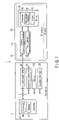
- FIG. 1 is an explanatory diagram for explaining an example of an IC card processing system 1.
- the IC card processing system 1 includes a host device 11, an IC card 12 (portable electronic device), and the like.
- the host device 11 and the IC card 12 are configured to be able to communicate with each other in a contact or non-contact manner.
- the IC card processing system 1 may include a configuration as necessary in addition to the configuration illustrated in FIG. 1 , or a specific configuration may be excluded from the IC card processing system 1.
- the host device 11 is an IC card processing device that processes the IC card 12.
- the host device 11 controls the entire IC card processing system 1.
- the host device 11 activates the IC card 12 by supplying electric power to the IC card 12.
- the host device 11 causes the IC card 12 to execute various operations by transmitting various commands to the IC card 12.
- the host device 11 includes a controller 21, a first card reader/writer 22, a second card reader/writer 23, a display 24, an operation interface 25, and the like.
- the controller 21 controls various operations of the host device 11.
- the controller 21 includes a processor 26 and a memory 27.
- the processor 26 includes an arithmetic element (for example, a CPU) that executes arithmetic processing.
- the processor 26 executes various operations by executing a program stored in the memory 27.
- the memory 27 stores the program, data for use in the program, and the like.
- the memory 27 includes, for example, a driver of the first card reader/writer 22, a driver of the second card reader/writer 23, a program for generating an image to be displayed on the display 24, and a program for interpreting an operation input by the operation interface 25. Further, the memory 27 includes a program for performing transmission of a command and reception of a response with the IC card 12. That is, the memory 27 stores a control program for the IC card processing device that processes the IC card 12.
- the first card reader/writer 22 is an interface for performing contact communication with the IC card 12.
- the first card reader/writer 22 includes a plurality of contact terminals physically and electrically connected to a contact pattern of the IC card 12, and a slot into which the IC card 12 is inserted.
- the first card reader/writer 22 transmits and receives data to and from the IC card 12 via the contact terminals and the contact pattern.
- the first card reader/writer 22 supplies electric power and a clock to the IC card 12 via the contact terminals and the contact pattern.
- the second card reader/writer 23 is an interface for performing non-contact communication with the IC card 12.
- the second card reader/writer 23 includes an antenna (coil) and a modulation/demodulation circuit.
- the second card reader/writer 23 modulates a signal corresponding to data to be transmitted by the modulation/demodulation circuit and causes the modulated signal to flow to the antenna, thereby causing the antenna to output a radio wave corresponding to the data.
- the second card reader/writer 23 receives a radio wave from the IC card through the antenna, demodulates the received signal by the modulation/demodulation circuit, and acquires original data.
- the first card reader/writer 22 supplies electric power to the IC card 12 by the radio wave from the antenna.
- the display 24 displays a screen based on data for display (screen data) supplied from the controller 21 or a graphic controller (not shown).
- the operation interface 25 is a configuration to generate an operation signal based on an operation.
- the operation interface 25 receives or generates an operation signal based on an operation of an operation member, such as a mouse, a trackball, a keyboard, a track pad, or a touch sensor, and supplies the operation signal to the controller 21.
- an operation member such as a mouse, a trackball, a keyboard, a track pad, or a touch sensor
- the host device 11 includes both the first card reader/writer 22 and the second card reader/writer 23, but the host device 11 may include at least one of the first card reader/writer 22 and the second card reader/writer 23. Further, the host device 11 may be configured to include a communication interface to which the first card reader/writer 22 or the second card reader/writer 23 is connected.
- the IC card 12 is activated by electric power supplied from the host device 11.
- the IC card 12 receives a command from the host device 11 and executes various processing in accordance with the received command.
- the IC card 12 generates a response according to the processing and transmits the response to the host device 11.
- the IC card 12 has a card-shaped main body 31 formed of plastic or the like.
- the IC card 12 includes an IC module 32 in the main body 31.
- the IC module 32 includes an IC chip 33, a contact communication interface 34, and a non-contact communication interface 35. That is, the IC card 12 is a dual interface card having the contact communication interface 34 for performing contact communication and the non-contact communication interface 35 for performing non-contact communication with the host device 11.
- the IC chip 33 includes a processor 36, a nonvolatile memory 37, and a RAM 38.
- the IC card 12 may have an additional element other than those shown in FIG. 1 , or a part of the configuration shown in FIG. 1 may be excluded from the IC card 12.
- the processor 36 includes an arithmetic element (for example, a CPU) that executes arithmetic processing.
- the processor 36 executes various operations by executing a program stored in the nonvolatile memory 37.
- the nonvolatile memory 37 is a nonvolatile memory that stores a program, data for use in the program, and the like.
- the program stored in the nonvolatile memory 37 is, for example, an operating system (OS) and an application for performing various processing according to an operation form of the IC card 12.
- the application is, for example, an IC card application managed by a card issuer (an entity that issued a card).
- the OS is an IC card control program for causing the processor 36 to realize control and information processing of each unit in the IC card 12.
- the program and control data in the nonvolatile memory 37 are incorporated in advance in accordance with the specification of the IC card 12 and the like.
- the IC card 12 may be configured to include a ROM that stores a control program for the IC card, such as an OS and applications.
- a file structure defined by ISO/IEC 7816 is configured in the nonvolatile memory 37.
- a master file (MF), a dedicated file (DF), an elementary file (EF), and the like are stored in the nonvolatile memory 37.
- the MF is a file that is the basis of the file structure.
- the DF is created at an order below the MF.
- the DF is a file in which applications and data to be used by the applications are grouped and stored.
- the EF is created at an order below the DF.
- the EF is a file for storing various data.
- the EF may be placed at an order immediately below the MF.
- the RAM 38 is a volatile memory that temporarily stores data.
- the RAM 38 temporarily stores data that is being processed by the processor 36, programs read from the nonvolatile memory 37, and the like.
- the RAM 38 functions as a calculation buffer, a reception buffer, and a transmission buffer.
- the calculation buffer is an area for temporarily holding results of various arithmetic processing executed by the processor 36.
- the reception buffer is an area for temporarily holding a command (command data) or the like received from the host device 11.
- the transmission buffer is an area for temporarily holding a response (response data) or the like to be transmitted to the host device 11.
- Some of the various functions realized by the processor 36 executing the program may be incorporated into the IC chip 33 as a hardware circuit. In this case, the processor 36 controls the functions performed by the hardware circuit.
- the contact communication interface 34 is contact communication means for performing contact communication with the host device 11.
- the contact communication interface 34 is connected to a terminal of the IC chip 33 and includes a contact pattern exposed on the surface of the IC card 12.
- the contact pattern is configured to be physically and electrically connected to the contact terminals when the IC card 12 is inserted into the slot of the first card reader/writer 22.
- the contact communication interface 34 relays electric power supply and data transmission/reception between the host device 11 and the IC chip 33.
- the non-contact communication interface 35 is non-contact communication means for performing non-contact communication with the host device 11.
- the non-contact communication interface 35 includes an antenna (coil), a modulation/demodulation circuit, and a power supply circuit.
- the non-contact communication interface 35 modulates a signal corresponding to data to be transmitted by the modulation/demodulation circuit and causes the modulated signal to flow to the antenna, thereby causing the antenna to output a radio wave corresponding to the data.
- the non-contact communication interface 35 receives a radio wave from the second card reader/writer 23 of the host device 11 through the antenna, demodulates the received signal by the modulation/demodulation circuit, and acquires the original data.
- the non-contact communication interface 35 rectifies and smooths, via a power supply circuit, an induced current generated in the antenna by a radio wave from the second card reader/writer 23 of the host device 11, and supplies a predetermined power supply voltage to the IC chip 33.
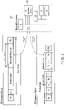
- FIG. 2 is an explanatory diagram for explaining an initial response from the IC card 12.
- the nonvolatile memory 37 of the IC card 12 includes a storage area for storing information (hereinafter referred to as characteristic information) indicating characteristics of the card mainly based on the card operation method of the IC card 12.
- the characteristic information is configured as historical bytes including, for example, "manufacturer identification information", “IC chip identification information”, “number of rewritable times", and "presence or absence of support for an extended format". That is, the nonvolatile memory 37 includes the storage area in which the historical bytes are stored.
- the historical bytes are stored in advance, for example, in a predetermined EF 41 at an order below the MF.
- the historical bytes may be stored, for example, in an EF at an order below the DF.
- the historical bytes may be stored in the nonvolatile memory 37 in a form other than the EF.
- the historical bytes may be stored in any storage area of the nonvolatile memory 37 in a state in which a tag indicating the historical bytes is added.
- the IC card 12 When activated, the IC card 12 performs an initial response. In the initial response, the IC card 12 transmits to the host device 11 information for performing setting related to communication between the host device 11 and the IC card 12.
- the IC card 12 is activated by a DC power supply voltage supplied from the host device 11 via the contact communication interface 34.
- the IC card 12 When the IC card 12 is activated, it performs an initial response based on ISO/IEC 7816 regulations. Specifically, the IC card 12 reads necessary information from the nonvolatile memory 37, and transmits to the host device 11 an answer to reset (ATR) whose frame format is defined by, for example, ISO/IEC 7816-3.
- ATR answer to reset
- the ATRs include "TS", “T0”, “Interface bytes”, “Historical characters”, “TSK”, and the like.
- the "Interface bytes” and the “Historical characters” are optional information.
- TS (Initial character TS) is information indicating a logic level of a signal and a bit transfer order.
- T0 (Format byte T0) is information indicating the presence or absence of "TA1", “TB1”, “TC1”, and “TD1" in the first set of "Interface bytes” and the length of "Historical characters”.
- the "Interface bytes" are information indicating, for example, a data transfer rate.
- the "Historical characters” are information (characteristic information) indicating a characteristic of the card mainly based on the card operation method of the IC card 12.
- the processor 36 of the IC card 12 reads the historical bytes from the EF 41 storing the historical bytes of the nonvolatile memory 37, and sets the historical bytes in the field of "Historical characters”.
- the “Historical characters” are data of 15 bytes at the maximum and are defined by ISO/IEC 7816-4.
- TCK is information indicating an exclusive OR of each character from “T0" to “TCK”.
- TCK is data of 32 bytes at the maximum.
- the IC card 12 By transmitting the ATR to the host device 11, the IC card 12 becomes able to perform contact communication with the host device 11.
- the host device 11 periodically performs polling (transmission of an initial response request command) while outputting radio waves for activating the IC card 12 through the antenna of the second card reader/writer 23.
- the initial response request command is, for example, Request command type B (REQB) or Request command type A (REQA) defined by ISO/IEC 14443.
- REQB Request command type B
- REQA Request command type A
- the IC card 12 rectifies and smooths an induced current generated in the antenna of the non-contact communication interface 35 by radio waves through the antenna of the second card reader/writer 23, and obtains a DC power supply voltage.
- the IC card 12 is activated by a DC power supply voltage.
- the IC card 12 transmits an initial response to the host device 11.
- the IC card 12 transmits an Answer To Request command type B (ATQB) or an Answer To Request command type A (ATQA) defined by, for example, ISO/IEC 14443 to the host device 11 as an initial response.
- the initial response includes a parameter indicating a response (initial response) to the initial response request command, a pseudo-unique IC card (PICC) identifier, application data indicating what application is written, protocol information indicating a supported protocol, a cyclic redundancy check code, and the like.
- PICC pseudo-unique IC card
- the host device 11 Upon receipt of the initial response, the host device 11 transmits to the IC card 12 a command for requesting the IC card 12 to provide information (characteristic information) indicating the characteristics of the card. Specifically, the host device 11 transmits a Request for Answer To Select (RATS) for requesting the IC card 12 to transmit an Answer To Select (ATS) to the IC card 12.
- RATS Answer To Select
- Frame formats of the ATS and the RATS are defined by ISO/IEC 14443.
- the IC card 12 When the transmission of the characteristic information is requested, the IC card 12 reads necessary information from the nonvolatile memory 37 and transmits the characteristic information to the host device 11. Specifically, upon receipt of the RATS, the IC card 12 reads the historical bytes from the EF 41 of the nonvolatile memory 37 and transmits to the host device 11 the ATS to which the historical bytes are added.
- the ATS includes "TL”, “T0”, “TA”, “TB”, “TC”, “historical bytes”, “cyclic redundancy check (CRC)", and the like.
- TL is information indicating the length of the ATS (length byte). The length indicated by “TL” does not include the byte of "CRC”.
- T0 is a format byte. "T0” indicates information, such as a presence or absence of subsequent "TA”, “TB”, “TC”, and “historical bytes”, and a receivable maximum frame length.
- TA indicates information on a communication speed.
- TB indicates information such as a frame waiting time and a start frame guard time.
- TC indicates whether "Card Identifier (CID)” or “Node Address (NAD)" is supported.
- the "historical bytes” are information (characteristic information) indicating a characteristic of the card mainly based on a card operation method of the IC card 12.
- the processor 36 of the IC card 12 reads the historical bytes from the EF 41 storing the historical bytes in the nonvolatile memory 37, and sets the read historical bytes to the "historical bytes" of the ATS.
- CRC is a code for use in error detection.
- the IC card 12 When the IC card 12 is of type A defined by ISO/IEC 14443, the IC card 12 transmits the aforementioned ATS to the host device 11, thereby enabling normal command processing by non-contact communication with the host device 11. In this case, the host device 11 can execute an arbitrary application stored in the DF by transmitting a SELECT command to the IC card 12.
- the host device 11 transmits ATTRIB to the IC card 12.
- the IC card 12 adds the ATS or the historical bytes to an Answer To ATTRIB (ATA), which is a response to the ATTRIB to the host device, and transmits the ATA or the historical bytes to the host device 11.
- ATA Answer To ATTRIB
- the processor 36 of the IC card 12 when transmitting the ATR to the host device 11 via the contact communication interface 34, the processor 36 of the IC card 12 reads the historical bytes from the EF 41 storing the historical bytes, adds the historical bytes to the ATR, and transmits the ATR.
- the processor 36 of the IC card 12 When transmitting the ATS to the host device 11 via the non-contact communication interface 35, the processor 36 of the IC card 12 reads the historical bytes from the EF 41 storing the historical bytes, adds the historical bytes to the ATS, and transmits the ATS.
- the processor 36 of the IC card 12 adds the historical bytes in the predetermined storage area (EF 41) of the nonvolatile memory 37 to the ATR in the contact communication and the ATS in the non-contact communication. That is, the processor 36 of the IC card 12 generates the ATR and the ATS using the historical bytes stored in the same storage area in the nonvolatile memory 37 both when transmitting the ATR and when transmitting the ATS.
- EF 41 predetermined storage area
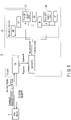
- FIG. 3 is an explanatory diagram for explaining rewriting of historical bytes stored in the nonvolatile memory 37 of the IC card 12.
- programs OS, applications, and the like executed by the processor 36 of the IC card 12 are illustrated in blocks.
- the host device 11 transmits a predetermined command, to which historical bytes for rewriting are added, to the IC card 12 through the first card reader/writer 22 or the second card reader/writer 23.
- the host device 11 causes the historical bytes of the nonvolatile memory 37 of the IC card 12 to be rewritten.
- the command to which the historical bytes for rewriting are added may be any arbitrary command.
- the format of the command transmitted from the host device 11 to the IC cards 12 is defined by ISO/IEC 7816, and includes fields such as "CLA”, “INS”, “P1", “P2”, “Lc”, “Data”, and "Le”.
- CLA is information indicating the type of the command.
- INS is information indicating the type of the command. The type of the command is indicated by “CLA” and "INS".
- P1 and P2 are information indicating parameters corresponding to "INS".
- P1" and P2 indicate, for example, command option designation.
- P1" and P2 indicate IDs of files to be processed.
- Lc is information indicating the data length (number of bytes) of "Data”.
- Data is information indicating the data body of the command. "Data” stores, for example, data to be used in command processing based on the command.
- Le is information indicating a data length (maximum length) of a response to the command.
- the host device 11 adds historical bytes for rewriting to "Data". That is, the host device 11 transmits to the IC card 12 a command in which historical bytes for rewriting are added to "Data".
- the OS of the IC card 12 recognizes the type of the received command by analyzing the values of "CLA” and "INS" of the received command.
- the OS of the IC card 12 executes processing according to the received command. For example, when receiving a command to which historical bytes for rewriting are added, the OS of the IC card 12 passes the received command to an application managed by the card issuer.
- the application of the IC card 12 sets the historical bytes for rewriting that have been added to "Data" of the command in, for example, a buffer area of the RAM 38. Furthermore, the application calculates an offset value of a storage area in the nonvolatile memory 37 in which the historical bytes are stored and a length of the historical bytes in the nonvolatile memory 37. That is, the application calculates an offset value to the head of the EF 41 in which the historical bytes for use in generating the ATR and the ATS are stored, and a length of the historical bytes in the EF 41 (or a length of the EF 41) in the nonvolatile memory 37.
- the application of the IC card 12 sets (overwrites) the historical bytes for rewriting that have been added to the command in the nonvolatile memory 37 using an application programming interface (API).
- the API recognizes the storage area to be overwritten based on the calculation result of the offset value and the calculation result of the length of the historical bytes, and overwrites the recognized storage area with the historical bytes for rewriting that have been added to the command.
- the application transmits a return value (response) indicating the processing result to the OS in accordance with the processing result.
- the API may be configured as a part of the application or may be configured as a part of the OS.
- the OS confirms the return value from the application and transmits a response to the host device 11 in accordance with the result.
- the format of the response transmitted from the IC card 12 to the host device 11 is defined by ISO/IEC 7816, and has fields such as "SW1" and "SW2".
- SW1 and SW2 are information (status bytes) indicating a processing result in the IC card 12.
- SW1 and “SW2" are values indicating a normal end, the host device 11 recognizes that the rewriting of the historical bytes has been normally performed in the IC card 12.
- the IC card 12 may be configured such that the OS sets the historical bytes for rewriting that have been added to "Data" of the command in the buffer. Further, the IC card 12 may be configured such that the OS calculates the offset value of the storage area in the nonvolatile memory 37 in which the historical bytes are stored and calculates the length of the historical bytes in the nonvolatile memory 37. In this case, the OS passes to the application the address at which the historical bytes in the buffer are set, the calculation result of the offset value, and the calculation result of the length of the historical byte.
- the storage area in which historical bytes are stored is provided in the nonvolatile memory 37 of the IC card 12.
- the processor 36 of the IC card 12 sets the ATR and the ATS based on the historical bytes in the nonvolatile memory 37. That is, the processor 36 reads the historical bytes from the storage area in which the historical bytes are stored in the nonvolatile memory 37, and adds the historical bytes to the ATR and the ATS.
- the processor 36 of the IC card 12 receives the predetermined command to which the historical bytes for rewriting are added, the processor 36 overwrites the historical bytes for rewriting on the storage area in which the historical bytes are stored in the nonvolatile memory 37.
- the historical bytes added to the ATR in the contact communication and the historical bytes added to the ATS in the non-contact communication are set based on the predetermined command including the historical bytes for rewriting. That is, both the historical bytes added to the ATR and the historical bytes added to the ATS are changed by one command. This eliminates the need to individually change the historical bytes added to the ATR and the historical bytes added to the ATS. As a result, the convenience of the IC card can be improved.
- the historical bytes are described as being read from the storage area in which the historical bytes are stored in the nonvolatile memory 37, and used for both generation of the ATR and generation of the ATS.
- the second embodiment is different from the first embodiment in that a storage area in which historical bytes for the ATR are stored and a storage area in which historical bytes for the ATS are stored are provided in the nonvolatile memory 37.
- the same components as those of the first embodiment are denoted by the same reference numerals, and redundant explanations will be omitted.
- FIG. 4 is an explanatory diagram for explaining an initial response from the IC card 12.
- the nonvolatile memory 37 of the IC card 12 is provided with a first EF 42 (first storage area) and a second EF 43 (second storage area).
- Historical bytes historical bytes for the ATR
- Historical bytes historical bytes for the ATS
- Historical bytes historical bytes for the ATS
- the historical bytes for the ATR and the historical bytes for the ATS are data having the same contents.
- the first EF 42 and the second EF 43 may be provided at an order below the MF.
- the historical bytes may be stored in the nonvolatile memory 37 in a form other than the EF.
- the historical bytes may be stored in any storage area of the nonvolatile memory 37 in a state in which a tag indicating that the historical bytes are historical bytes for the ATR or historical bytes for the ATS is added.
- the IC card 12 when the IC card 12 is activated, it performs an initial response based on ISO/IEC 7816 regulations. Specifically, the IC card 12 reads the historical bytes for the ATR from the first EF 42 of the nonvolatile memory 37, and transmits to the host device 11 the ATR to which the historical bytes for the ATR are added. As a result, the IC card 12 becomes able to perform contact communication with the host device 11.
- the IC card 12 when the IC card 12 is activated, it transmits an initial response to the host device 11 based on the ISO/IEC 14443 regulations.
- the host device 11 Upon receipt of the initial response, the host device 11 transmits a command for requesting feature information to the IC card 12.
- the IC card 12 Upon receipt of the command for requesting the feature information, the IC card 12 reads the historical bytes for the ATS from the second EF 43 of the nonvolatile memory 37, and transmits to the host device 11 the ATS to which the historical bytes for the ATS are added. Thus, normal command processing by non-contact communication is enabled between the host device 11 and the IC card 12.
- the command for requesting the characteristic information is RATS when the IC card 12 is of type A defined by ISO/IEC 14443.
- the IC card 12 transmits the ATS to the host device 11 in response to the reception of the RATS.
- the command for requesting the characteristic information is ATTRIB when the IC card 12 is of type B defined by ISO/IEC 14443.
- the IC card 12 generates an ATA in response to the reception of the ATTRIB, adds the ATS to the ATA, and transmits the ATA to the host device 11.
- FIG. 5 is an explanatory diagram for explaining rewriting of historical bytes stored in the nonvolatile memory 37 of the IC card 12.
- programs OS, applications, and the like executed by the processor 36 of the IC card 12 are illustrated in blocks.
- the host device 11 transmits a predetermined command, to which historical bytes for rewriting are added, to the IC card 12 through the first card reader/writer 22 or the second card reader/writer 23.
- the OS of the IC card 12 recognizes the type of the received command by analyzing the values of "CLA” and "INS" of the received command.
- the OS of the IC card 12 executes processing according to the received command. For example, when receiving a predetermined command to which historical bytes for rewriting are added, the OS of the IC card 12 passes the received command to an application managed by the card issuer.
- the application of the IC card 12 sets the historical bytes for rewriting that have been added to "Data" of the command in, for example, a buffer area of the RAM 38.
- the application calculates an offset value of a storage area in the nonvolatile memory 37 in which the historical bytes for the ATR are stored and a length of the historical bytes for the ATR in the nonvolatile memory 37.
- the application calculates an offset value of a storage area in the nonvolatile memory 37 in which the historical bytes for the ATS are stored and a length of the historical bytes for the ATS in the nonvolatile memory 37.
- the application calculates an offset value to the head of each of the first EF 42 and the second EF 43 in which the historical bytes for the ATR and the historical bytes for the ATS are stored, and a length of the historical bytes in the nonvolatile memory 37.
- the application of the IC card 12 acquires the historical bytes for rewriting from "Data" of the command, and sets (overwrites) the acquired historical bytes for rewriting to the historical bytes for the ATR of the first EF 42 and the historical bytes for the ATS of the second EF 43.
- the application transmits a return value (response) indicating the processing result to the OS in accordance with the processing result.
- the OS confirms the return value from the application and transmits a response to the host device 11 in accordance with the result.
- the first storage area for storing the historical bytes for the ATR and the second storage area for storing the historical bytes for the ATS are separately provided.
- the processor 36 of the IC card 12 rewrites both the first storage area and the second storage area based on a predetermined command including historical bytes for rewriting. That is, the processor 36 overwrites both the historical bytes for the ATR in the first storage area and the historical bytes for the ATS in the second storage area with the historical bytes for rewriting included in the predetermined command.
- the processor 36 adds the historical bytes for the ATR in the first storage area to the ATR in the contact communication. Further, the processor 36 of the IC card 12 adds the historical bytes for the ATS in the second storage area to the ATS in the non-contact communication.
- the historical bytes added to the ATR in the contact communication and the historical bytes added to the ATS in the non-contact communication are also changed based on the predetermined command including the historical bytes for rewriting. That is, both the historical bytes added to the ATR and the historical bytes added to the ATS are changed by one command. This eliminates the need to individually change the historical bytes added to the ATR and the historical bytes added to the ATS. As a result, the convenience of the IC card can be improved.
- each of the embodiments are not only limited to those configured using hardware, and may be implemented using software by causing a computer to read a program in which each function is described.
- each function may be configured by appropriately selecting either software or hardware.
Landscapes
- Engineering & Computer Science (AREA)
- Computer Hardware Design (AREA)
- Microelectronics & Electronic Packaging (AREA)
- Physics & Mathematics (AREA)
- General Physics & Mathematics (AREA)
- Theoretical Computer Science (AREA)
- Computer Security & Cryptography (AREA)
- General Engineering & Computer Science (AREA)
- Computer Networks & Wireless Communication (AREA)
- Credit Cards Or The Like (AREA)
- Information Transfer Systems (AREA)
Abstract
Description
- Embodiments described herein relate generally to an IC card and a control program for the IC card.
- An IC card (portable electronic device) including an IC chip having a processor, a nonvolatile memory, a random access memory (RAM), and a communication interface has been put into practical use. Further, a dual interface card, which is an IC card having a contact communication interface for performing contact communication and a non-contact communication interface for performing non-contact communication, has been generally put into practical use.
- The IC card transmits, to a host device, information indicating characteristics of the card, such as a manufacturer, information about a chip, the number of rewritable times, and a presence or absence of support for a format using an extended length (referred to as an extended format). The information indicating the characteristics of the card is, for example, historical bytes defined by ISO/IEC 7816. When the IC card performs contact communication with a host device, the IC card transmits an Answer To Reset (ATR) including a historical byte to the host device. When the IC card performs non-contact communication with a host device, the IC card transmits an Answer To Select (ATS) including historical bytes to the host device.
- There are various methods for rewriting the historical bytes included in the ATR, such as "setATRHistBytes" defined in "GPSystem" of "globalplatform". However, in the above method, there is a problem in that the historical bytes included in the ATS cannot be rewritten.
- Patent Literature 1: Jpn. Pat. Appln. KOKAI Publication No.
2003-288561 - An object of the present invention is to provide a highly convenient IC card and a control program for the IC card.
- An IC card according to an embodiment includes a contact communication interface, a non-contact communication interface, and a processor. A contact communication means is configured to perform contact communication with a reader/writer. A non-contact communication means is configured to perform non-contact communication with the reader/writer. The processor is configured to set an Answer To Reset (ATR) in the contact communication and an Answer To Select (ATS) in the non-contact communication based on a predetermined command including historical bytes.
-
-
FIG. 1 is an explanatory diagram for explaining a configuration example of an IC card processing system according to an embodiment. -
FIG. 2 is an explanatory diagram for explaining an example of an operation of the IC card according to a first embodiment. -
FIG. 3 is an explanatory diagram for explaining an example of an operation of the IC card according to the first embodiment. -
FIG. 4 is an explanatory diagram for explaining an example of an operation of the IC card according to a second embodiment. -
FIG. 5 is an explanatory diagram for explaining an example of an operation of the IC card according to the second embodiment. - Hereinafter, the embodiments will be described with reference to the accompanying drawings.
-
FIG. 1 is an explanatory diagram for explaining an example of an ICcard processing system 1. - The IC
card processing system 1 includes ahost device 11, an IC card 12 (portable electronic device), and the like. Thehost device 11 and theIC card 12 are configured to be able to communicate with each other in a contact or non-contact manner. Note that the ICcard processing system 1 may include a configuration as necessary in addition to the configuration illustrated inFIG. 1 , or a specific configuration may be excluded from the ICcard processing system 1. - First, the configuration of the
host device 11 will be described. - The
host device 11 is an IC card processing device that processes theIC card 12. Thehost device 11 controls the entire ICcard processing system 1. Thehost device 11 activates theIC card 12 by supplying electric power to theIC card 12. In addition, thehost device 11 causes theIC card 12 to execute various operations by transmitting various commands to theIC card 12. - The
host device 11 includes acontroller 21, a first card reader/writer 22, a second card reader/writer 23, adisplay 24, anoperation interface 25, and the like. - The
controller 21 controls various operations of thehost device 11. Thecontroller 21 includes aprocessor 26 and amemory 27. - The
processor 26 includes an arithmetic element (for example, a CPU) that executes arithmetic processing. Theprocessor 26 executes various operations by executing a program stored in thememory 27. - The
memory 27 stores the program, data for use in the program, and the like. Thememory 27 includes, for example, a driver of the first card reader/writer 22, a driver of the second card reader/writer 23, a program for generating an image to be displayed on thedisplay 24, and a program for interpreting an operation input by theoperation interface 25. Further, thememory 27 includes a program for performing transmission of a command and reception of a response with theIC card 12. That is, thememory 27 stores a control program for the IC card processing device that processes theIC card 12. - The first card reader/
writer 22 is an interface for performing contact communication with theIC card 12. The first card reader/writer 22 includes a plurality of contact terminals physically and electrically connected to a contact pattern of theIC card 12, and a slot into which theIC card 12 is inserted. The first card reader/writer 22 transmits and receives data to and from theIC card 12 via the contact terminals and the contact pattern. The first card reader/writer 22 supplies electric power and a clock to theIC card 12 via the contact terminals and the contact pattern. - The second card reader/
writer 23 is an interface for performing non-contact communication with theIC card 12. The second card reader/writer 23 includes an antenna (coil) and a modulation/demodulation circuit. The second card reader/writer 23 modulates a signal corresponding to data to be transmitted by the modulation/demodulation circuit and causes the modulated signal to flow to the antenna, thereby causing the antenna to output a radio wave corresponding to the data. The second card reader/writer 23 receives a radio wave from the IC card through the antenna, demodulates the received signal by the modulation/demodulation circuit, and acquires original data. Furthermore, the first card reader/writer 22 supplies electric power to theIC card 12 by the radio wave from the antenna. - The
display 24 displays a screen based on data for display (screen data) supplied from thecontroller 21 or a graphic controller (not shown). - The
operation interface 25 is a configuration to generate an operation signal based on an operation. Theoperation interface 25 receives or generates an operation signal based on an operation of an operation member, such as a mouse, a trackball, a keyboard, a track pad, or a touch sensor, and supplies the operation signal to thecontroller 21. - In the example of
FIG. 1 , thehost device 11 includes both the first card reader/writer 22 and the second card reader/writer 23, but thehost device 11 may include at least one of the first card reader/writer 22 and the second card reader/writer 23. Further, thehost device 11 may be configured to include a communication interface to which the first card reader/writer 22 or the second card reader/writer 23 is connected. - Next, a configuration of the
IC card 12 will be described. - The
IC card 12 is activated by electric power supplied from thehost device 11. TheIC card 12 receives a command from thehost device 11 and executes various processing in accordance with the received command. In addition, theIC card 12 generates a response according to the processing and transmits the response to thehost device 11. - The
IC card 12 has a card-shapedmain body 31 formed of plastic or the like. TheIC card 12 includes anIC module 32 in themain body 31. TheIC module 32 includes anIC chip 33, acontact communication interface 34, and anon-contact communication interface 35. That is, theIC card 12 is a dual interface card having thecontact communication interface 34 for performing contact communication and thenon-contact communication interface 35 for performing non-contact communication with thehost device 11. TheIC chip 33 includes aprocessor 36, anonvolatile memory 37, and aRAM 38. TheIC card 12 may have an additional element other than those shown inFIG. 1 , or a part of the configuration shown inFIG. 1 may be excluded from theIC card 12. - The
processor 36 includes an arithmetic element (for example, a CPU) that executes arithmetic processing. Theprocessor 36 executes various operations by executing a program stored in thenonvolatile memory 37. - The
nonvolatile memory 37 is a nonvolatile memory that stores a program, data for use in the program, and the like. The program stored in thenonvolatile memory 37 is, for example, an operating system (OS) and an application for performing various processing according to an operation form of theIC card 12. The application is, for example, an IC card application managed by a card issuer (an entity that issued a card). The OS is an IC card control program for causing theprocessor 36 to realize control and information processing of each unit in theIC card 12. The program and control data in thenonvolatile memory 37 are incorporated in advance in accordance with the specification of theIC card 12 and the like. Note that theIC card 12 may be configured to include a ROM that stores a control program for the IC card, such as an OS and applications. - A file structure defined by ISO/IEC 7816 is configured in the
nonvolatile memory 37. For example, a master file (MF), a dedicated file (DF), an elementary file (EF), and the like are stored in thenonvolatile memory 37. - The MF is a file that is the basis of the file structure.
- The DF is created at an order below the MF. The DF is a file in which applications and data to be used by the applications are grouped and stored.
- The EF is created at an order below the DF. The EF is a file for storing various data. The EF may be placed at an order immediately below the MF.
- The
RAM 38 is a volatile memory that temporarily stores data. TheRAM 38 temporarily stores data that is being processed by theprocessor 36, programs read from thenonvolatile memory 37, and the like. For example, theRAM 38 functions as a calculation buffer, a reception buffer, and a transmission buffer. The calculation buffer is an area for temporarily holding results of various arithmetic processing executed by theprocessor 36. The reception buffer is an area for temporarily holding a command (command data) or the like received from thehost device 11. The transmission buffer is an area for temporarily holding a response (response data) or the like to be transmitted to thehost device 11. - Some of the various functions realized by the
processor 36 executing the program may be incorporated into theIC chip 33 as a hardware circuit. In this case, theprocessor 36 controls the functions performed by the hardware circuit. - The
contact communication interface 34 is contact communication means for performing contact communication with thehost device 11. For example, thecontact communication interface 34 is connected to a terminal of theIC chip 33 and includes a contact pattern exposed on the surface of theIC card 12. The contact pattern is configured to be physically and electrically connected to the contact terminals when theIC card 12 is inserted into the slot of the first card reader/writer 22. Thecontact communication interface 34 relays electric power supply and data transmission/reception between thehost device 11 and theIC chip 33. - The
non-contact communication interface 35 is non-contact communication means for performing non-contact communication with thehost device 11. For example, thenon-contact communication interface 35 includes an antenna (coil), a modulation/demodulation circuit, and a power supply circuit. Thenon-contact communication interface 35 modulates a signal corresponding to data to be transmitted by the modulation/demodulation circuit and causes the modulated signal to flow to the antenna, thereby causing the antenna to output a radio wave corresponding to the data. Further, thenon-contact communication interface 35 receives a radio wave from the second card reader/writer 23 of thehost device 11 through the antenna, demodulates the received signal by the modulation/demodulation circuit, and acquires the original data. In addition, thenon-contact communication interface 35 rectifies and smooths, via a power supply circuit, an induced current generated in the antenna by a radio wave from the second card reader/writer 23 of thehost device 11, and supplies a predetermined power supply voltage to theIC chip 33. - Next, operations such as activation and initial response of the
IC card 12 according to the first embodiment will be described. -
FIG. 2 is an explanatory diagram for explaining an initial response from theIC card 12. - The
nonvolatile memory 37 of theIC card 12 includes a storage area for storing information (hereinafter referred to as characteristic information) indicating characteristics of the card mainly based on the card operation method of theIC card 12. The characteristic information is configured as historical bytes including, for example, "manufacturer identification information", "IC chip identification information", "number of rewritable times", and "presence or absence of support for an extended format". That is, thenonvolatile memory 37 includes the storage area in which the historical bytes are stored. - In the example of
FIG. 2 , the historical bytes are stored in advance, for example, in apredetermined EF 41 at an order below the MF. The historical bytes may be stored, for example, in an EF at an order below the DF. The historical bytes may be stored in thenonvolatile memory 37 in a form other than the EF. For example, the historical bytes may be stored in any storage area of thenonvolatile memory 37 in a state in which a tag indicating the historical bytes is added. - When activated, the
IC card 12 performs an initial response. In the initial response, theIC card 12 transmits to thehost device 11 information for performing setting related to communication between thehost device 11 and theIC card 12. - First, the contact communication will be described.
- In the contact communication, the
IC card 12 is activated by a DC power supply voltage supplied from thehost device 11 via thecontact communication interface 34. When theIC card 12 is activated, it performs an initial response based on ISO/IEC 7816 regulations. Specifically, theIC card 12 reads necessary information from thenonvolatile memory 37, and transmits to thehost device 11 an answer to reset (ATR) whose frame format is defined by, for example, ISO/IEC 7816-3. - As shown in
FIG. 2 , the ATRs include "TS", "T0", "Interface bytes", "Historical characters", "TSK", and the like. The "Interface bytes" and the "Historical characters" are optional information. - "TS (Initial character TS)" is information indicating a logic level of a signal and a bit transfer order.
- "T0 (Format byte T0)" is information indicating the presence or absence of "TA1", "TB1", "TC1", and "TD1" in the first set of "Interface bytes" and the length of "Historical characters".
- The "Interface bytes" indicate various parameters on the data transfer protocol.
- The "Interface bytes" are information indicating, for example, a data transfer rate.
- The "Historical characters" are information (characteristic information) indicating a characteristic of the card mainly based on the card operation method of the
IC card 12. For example, theprocessor 36 of theIC card 12 reads the historical bytes from theEF 41 storing the historical bytes of thenonvolatile memory 37, and sets the historical bytes in the field of "Historical characters". The "Historical characters" are data of 15 bytes at the maximum and are defined by ISO/IEC 7816-4. - "TCK" is information indicating an exclusive OR of each character from "T0" to "TCK". "TCK" is data of 32 bytes at the maximum.
- By transmitting the ATR to the
host device 11, theIC card 12 becomes able to perform contact communication with thehost device 11. - Next, non-contact communication will be described.
- In the non-contact communication, the
host device 11 periodically performs polling (transmission of an initial response request command) while outputting radio waves for activating theIC card 12 through the antenna of the second card reader/writer 23. - The initial response request command is, for example, Request command type B (REQB) or Request command type A (REQA) defined by ISO/IEC 14443.
- The
IC card 12 rectifies and smooths an induced current generated in the antenna of thenon-contact communication interface 35 by radio waves through the antenna of the second card reader/writer 23, and obtains a DC power supply voltage. TheIC card 12 is activated by a DC power supply voltage. When theIC card 12 is activated and receives an initial response request command from thehost device 11, theIC card 12 transmits an initial response to thehost device 11. - To be more specific, the
IC card 12 transmits an Answer To Request command type B (ATQB) or an Answer To Request command type A (ATQA) defined by, for example, ISO/IEC 14443 to thehost device 11 as an initial response. The initial response includes a parameter indicating a response (initial response) to the initial response request command, a pseudo-unique IC card (PICC) identifier, application data indicating what application is written, protocol information indicating a supported protocol, a cyclic redundancy check code, and the like. - Upon receipt of the initial response, the
host device 11 transmits to the IC card 12 a command for requesting theIC card 12 to provide information (characteristic information) indicating the characteristics of the card. Specifically, thehost device 11 transmits a Request for Answer To Select (RATS) for requesting theIC card 12 to transmit an Answer To Select (ATS) to theIC card 12. Frame formats of the ATS and the RATS are defined by ISO/IEC 14443. - When the transmission of the characteristic information is requested, the
IC card 12 reads necessary information from thenonvolatile memory 37 and transmits the characteristic information to thehost device 11. Specifically, upon receipt of the RATS, theIC card 12 reads the historical bytes from theEF 41 of thenonvolatile memory 37 and transmits to thehost device 11 the ATS to which the historical bytes are added. - As illustrated in
FIG. 2 , the ATS includes "TL", "T0", "TA", "TB", "TC", "historical bytes", "cyclic redundancy check (CRC)", and the like. - "TL" is information indicating the length of the ATS (length byte). The length indicated by "TL" does not include the byte of "CRC".
- "T0" is a format byte. "T0" indicates information, such as a presence or absence of subsequent "TA", "TB", "TC", and "historical bytes", and a receivable maximum frame length.
- "TA", "TB", and "TC" are interface bytes. "TA" indicates information on a communication speed. "TB" indicates information such as a frame waiting time and a start frame guard time. "TC" indicates whether "Card Identifier (CID)" or "Node Address (NAD)" is supported.
- The "historical bytes" are information (characteristic information) indicating a characteristic of the card mainly based on a card operation method of the
IC card 12. For example, theprocessor 36 of theIC card 12 reads the historical bytes from theEF 41 storing the historical bytes in thenonvolatile memory 37, and sets the read historical bytes to the "historical bytes" of the ATS. - "CRC" is a code for use in error detection.
- When the
IC card 12 is of type A defined by ISO/IEC 14443, theIC card 12 transmits the aforementioned ATS to thehost device 11, thereby enabling normal command processing by non-contact communication with thehost device 11. In this case, thehost device 11 can execute an arbitrary application stored in the DF by transmitting a SELECT command to theIC card 12. - When the
IC card 12 is of type B defined by ISO/IEC 14443, thehost device 11 transmits ATTRIB to theIC card 12. TheIC card 12 adds the ATS or the historical bytes to an Answer To ATTRIB (ATA), which is a response to the ATTRIB to the host device, and transmits the ATA or the historical bytes to thehost device 11. Thus, normal command processing by non-contact communication is enabled between theIC card 12 and thehost device 11. - As described above, when transmitting the ATR to the
host device 11 via thecontact communication interface 34, theprocessor 36 of theIC card 12 reads the historical bytes from theEF 41 storing the historical bytes, adds the historical bytes to the ATR, and transmits the ATR. - When transmitting the ATS to the
host device 11 via thenon-contact communication interface 35, theprocessor 36 of theIC card 12 reads the historical bytes from theEF 41 storing the historical bytes, adds the historical bytes to the ATS, and transmits the ATS. - As described above, the
processor 36 of theIC card 12 adds the historical bytes in the predetermined storage area (EF 41) of thenonvolatile memory 37 to the ATR in the contact communication and the ATS in the non-contact communication. That is, theprocessor 36 of theIC card 12 generates the ATR and the ATS using the historical bytes stored in the same storage area in thenonvolatile memory 37 both when transmitting the ATR and when transmitting the ATS. - Next, rewriting of the historical bytes in the first embodiment will be described.
-
FIG. 3 is an explanatory diagram for explaining rewriting of historical bytes stored in thenonvolatile memory 37 of theIC card 12. InFIG. 3 , programs (OS, applications, and the like) executed by theprocessor 36 of theIC card 12 are illustrated in blocks. - The
host device 11 transmits a predetermined command, to which historical bytes for rewriting are added, to theIC card 12 through the first card reader/writer 22 or the second card reader/writer 23. Thus, thehost device 11 causes the historical bytes of thenonvolatile memory 37 of theIC card 12 to be rewritten. The command to which the historical bytes for rewriting are added may be any arbitrary command. - The format of the command transmitted from the
host device 11 to theIC cards 12 is defined by ISO/IEC 7816, and includes fields such as "CLA", "INS", "P1", "P2", "Lc", "Data", and "Le". - "CLA" is information indicating the type of the command. "INS" is information indicating the type of the command. The type of the command is indicated by "CLA" and "INS".
- "P1" and "P2" are information indicating parameters corresponding to "INS". "P1" and "P2" indicate, for example, command option designation. For example, "P1" and "P2" indicate IDs of files to be processed.
- "Lc" is information indicating the data length (number of bytes) of "Data".
- "Data" is information indicating the data body of the command. "Data" stores, for example, data to be used in command processing based on the command.
- "Le" is information indicating a data length (maximum length) of a response to the command.
- The
host device 11 adds historical bytes for rewriting to "Data". That is, thehost device 11 transmits to the IC card 12 a command in which historical bytes for rewriting are added to "Data". - The OS of the
IC card 12 recognizes the type of the received command by analyzing the values of "CLA" and "INS" of the received command. The OS of theIC card 12 executes processing according to the received command. For example, when receiving a command to which historical bytes for rewriting are added, the OS of theIC card 12 passes the received command to an application managed by the card issuer. - The application of the
IC card 12 sets the historical bytes for rewriting that have been added to "Data" of the command in, for example, a buffer area of theRAM 38. Furthermore, the application calculates an offset value of a storage area in thenonvolatile memory 37 in which the historical bytes are stored and a length of the historical bytes in thenonvolatile memory 37. That is, the application calculates an offset value to the head of theEF 41 in which the historical bytes for use in generating the ATR and the ATS are stored, and a length of the historical bytes in the EF 41 (or a length of the EF 41) in thenonvolatile memory 37. - The application of the
IC card 12 sets (overwrites) the historical bytes for rewriting that have been added to the command in thenonvolatile memory 37 using an application programming interface (API). The API recognizes the storage area to be overwritten based on the calculation result of the offset value and the calculation result of the length of the historical bytes, and overwrites the recognized storage area with the historical bytes for rewriting that have been added to the command. The application transmits a return value (response) indicating the processing result to the OS in accordance with the processing result. Note that the API may be configured as a part of the application or may be configured as a part of the OS. - The OS confirms the return value from the application and transmits a response to the
host device 11 in accordance with the result. The format of the response transmitted from theIC card 12 to thehost device 11 is defined by ISO/IEC 7816, and has fields such as "SW1" and "SW2". - "SW1" and "SW2" are information (status bytes) indicating a processing result in the
IC card 12. When "SW1" and "SW2" are values indicating a normal end, thehost device 11 recognizes that the rewriting of the historical bytes has been normally performed in theIC card 12. - The
IC card 12 may be configured such that the OS sets the historical bytes for rewriting that have been added to "Data" of the command in the buffer. Further, theIC card 12 may be configured such that the OS calculates the offset value of the storage area in thenonvolatile memory 37 in which the historical bytes are stored and calculates the length of the historical bytes in thenonvolatile memory 37. In this case, the OS passes to the application the address at which the historical bytes in the buffer are set, the calculation result of the offset value, and the calculation result of the length of the historical byte. - As described above, the storage area in which historical bytes are stored is provided in the
nonvolatile memory 37 of theIC card 12. Theprocessor 36 of theIC card 12 sets the ATR and the ATS based on the historical bytes in thenonvolatile memory 37. That is, theprocessor 36 reads the historical bytes from the storage area in which the historical bytes are stored in thenonvolatile memory 37, and adds the historical bytes to the ATR and the ATS. When theprocessor 36 of theIC card 12 receives the predetermined command to which the historical bytes for rewriting are added, theprocessor 36 overwrites the historical bytes for rewriting on the storage area in which the historical bytes are stored in thenonvolatile memory 37. - Thus, the historical bytes added to the ATR in the contact communication and the historical bytes added to the ATS in the non-contact communication are set based on the predetermined command including the historical bytes for rewriting. That is, both the historical bytes added to the ATR and the historical bytes added to the ATS are changed by one command. This eliminates the need to individually change the historical bytes added to the ATR and the historical bytes added to the ATS. As a result, the convenience of the IC card can be improved.
- Next, operations such as activation and initial response of the
IC card 12 according to the second embodiment will be described. In the first embodiment, the historical bytes are described as being read from the storage area in which the historical bytes are stored in thenonvolatile memory 37, and used for both generation of the ATR and generation of the ATS. The second embodiment is different from the first embodiment in that a storage area in which historical bytes for the ATR are stored and a storage area in which historical bytes for the ATS are stored are provided in thenonvolatile memory 37. The same components as those of the first embodiment are denoted by the same reference numerals, and redundant explanations will be omitted. -
FIG. 4 is an explanatory diagram for explaining an initial response from theIC card 12. - As shown in
FIG. 4 , thenonvolatile memory 37 of theIC card 12 according to the second embodiment is provided with a first EF 42 (first storage area) and a second EF 43 (second storage area). Historical bytes (historical bytes for the ATR) to be used when generating the ATR are stored in, for example, afirst EF 42 at an order below a DF. Historical bytes (historical bytes for the ATS) to be used when generating the ATS are stored in, for example, asecond EF 43 different from thefirst EF 42. The historical bytes for the ATR and the historical bytes for the ATS are data having the same contents. - Further, the
first EF 42 and thesecond EF 43 may be provided at an order below the MF. Furthermore, the historical bytes may be stored in thenonvolatile memory 37 in a form other than the EF. For example, the historical bytes may be stored in any storage area of thenonvolatile memory 37 in a state in which a tag indicating that the historical bytes are historical bytes for the ATR or historical bytes for the ATS is added. - First, the contact communication will be described.
- For example, in contact communication, when the
IC card 12 is activated, it performs an initial response based on ISO/IEC 7816 regulations. Specifically, theIC card 12 reads the historical bytes for the ATR from thefirst EF 42 of thenonvolatile memory 37, and transmits to thehost device 11 the ATR to which the historical bytes for the ATR are added. As a result, theIC card 12 becomes able to perform contact communication with thehost device 11. - Next, non-contact communication will be described.
- For example, in the non-contact communication, when the
IC card 12 is activated, it transmits an initial response to thehost device 11 based on the ISO/IEC 14443 regulations. - Upon receipt of the initial response, the
host device 11 transmits a command for requesting feature information to theIC card 12. - Upon receipt of the command for requesting the feature information, the
IC card 12 reads the historical bytes for the ATS from thesecond EF 43 of thenonvolatile memory 37, and transmits to thehost device 11 the ATS to which the historical bytes for the ATS are added. Thus, normal command processing by non-contact communication is enabled between thehost device 11 and theIC card 12. - The command for requesting the characteristic information is RATS when the
IC card 12 is of type A defined by ISO/IEC 14443. In this case, theIC card 12 transmits the ATS to thehost device 11 in response to the reception of the RATS. - The command for requesting the characteristic information is ATTRIB when the
IC card 12 is of type B defined by ISO/IEC 14443. In this case, theIC card 12 generates an ATA in response to the reception of the ATTRIB, adds the ATS to the ATA, and transmits the ATA to thehost device 11. - Next, rewriting of the historical bytes in the second embodiment will be described.
-
FIG. 5 is an explanatory diagram for explaining rewriting of historical bytes stored in thenonvolatile memory 37 of theIC card 12. InFIG. 5 , programs (OS, applications, and the like) executed by theprocessor 36 of theIC card 12 are illustrated in blocks. - The
host device 11 transmits a predetermined command, to which historical bytes for rewriting are added, to theIC card 12 through the first card reader/writer 22 or the second card reader/writer 23. - The OS of the
IC card 12 recognizes the type of the received command by analyzing the values of "CLA" and "INS" of the received command. The OS of theIC card 12 executes processing according to the received command. For example, when receiving a predetermined command to which historical bytes for rewriting are added, the OS of theIC card 12 passes the received command to an application managed by the card issuer. - The application of the
IC card 12 sets the historical bytes for rewriting that have been added to "Data" of the command in, for example, a buffer area of theRAM 38. In addition, the application calculates an offset value of a storage area in thenonvolatile memory 37 in which the historical bytes for the ATR are stored and a length of the historical bytes for the ATR in thenonvolatile memory 37. In addition, the application calculates an offset value of a storage area in thenonvolatile memory 37 in which the historical bytes for the ATS are stored and a length of the historical bytes for the ATS in thenonvolatile memory 37. That is, the application calculates an offset value to the head of each of thefirst EF 42 and thesecond EF 43 in which the historical bytes for the ATR and the historical bytes for the ATS are stored, and a length of the historical bytes in thenonvolatile memory 37. - The application of the
IC card 12 acquires the historical bytes for rewriting from "Data" of the command, and sets (overwrites) the acquired historical bytes for rewriting to the historical bytes for the ATR of thefirst EF 42 and the historical bytes for the ATS of thesecond EF 43. The application transmits a return value (response) indicating the processing result to the OS in accordance with the processing result. - The OS confirms the return value from the application and transmits a response to the
host device 11 in accordance with the result. - As described above, in the
nonvolatile memory 37 of theIC card 12 according to the second embodiment, the first storage area for storing the historical bytes for the ATR and the second storage area for storing the historical bytes for the ATS are separately provided. Theprocessor 36 of theIC card 12 rewrites both the first storage area and the second storage area based on a predetermined command including historical bytes for rewriting. That is, theprocessor 36 overwrites both the historical bytes for the ATR in the first storage area and the historical bytes for the ATS in the second storage area with the historical bytes for rewriting included in the predetermined command. Theprocessor 36 adds the historical bytes for the ATR in the first storage area to the ATR in the contact communication. Further, theprocessor 36 of theIC card 12 adds the historical bytes for the ATS in the second storage area to the ATS in the non-contact communication. - According to the above configuration, the historical bytes added to the ATR in the contact communication and the historical bytes added to the ATS in the non-contact communication are also changed based on the predetermined command including the historical bytes for rewriting. That is, both the historical bytes added to the ATR and the historical bytes added to the ATS are changed by one command. This eliminates the need to individually change the historical bytes added to the ATR and the historical bytes added to the ATS. As a result, the convenience of the IC card can be improved.
- The functions described above for each of the embodiments are not only limited to those configured using hardware, and may be implemented using software by causing a computer to read a program in which each function is described. In addition, each function may be configured by appropriately selecting either software or hardware.
- While certain embodiments have been described, these embodiments have been presented by way of example only, and are not intended to limit the scope of the invention. The novel embodiments described herein can be implemented in a variety of other forms; furthermore, various omissions, substitutions, and changes can be made without departing from the spirit of the invention. The embodiments and their modifications are covered by the accompanying claims and their equivalents, as would fall within the scope and gist of the inventions.
Claims (5)
- An IC card comprising:a contact communication interface configured to perform contact communication with a reader/writer;a non-contact communication interface configured to perform non-contact communication with the reader/writer; anda processor configured to set an Answer To Reset (ATR) in the contact communication and an Answer To Select (ATS) in the non-contact communication based on historical bytes included in a predetermined command.
- The IC card according to claim 1, further comprising a nonvolatile memory including a storage area in which the historical bytes are stored, wherein
the processor is configured to add the historical bytes in the storage area of the nonvolatile memory to the ATR and the ATS. - The IC card according to claim 2, wherein the processor is configured to rewrite the historical bytes in the storage area of the nonvolatile memory based on the predetermined command including the historical bytes.
- The IC card according to claim 1, further comprising a nonvolatile memory including a first storage area and a second storage area, wherein
the processor is configured to:overwrite the first storage area and the second storage area with the historical bytes included in the predetermined command;add the historical bytes in the first storage area to the ATR; andadd the historical bytes in the second storage area to the ATS. - A control program for an IC card to be executed in an IC card including a contact communication interface configured to perform contact communication with a reader/writer, a non-contact communication interface configured to perform non-contact communication with the reader writer, and a processor, wherein
the control program causes the processor to set an Answer To Reset (ATR) in the contact communication and an Answer To Select (ATS) in the non-contact communication based on historical bytes included in a predetermined command.
Applications Claiming Priority (2)
| Application Number | Priority Date | Filing Date | Title |
|---|---|---|---|
| JP2019230798A JP7433886B2 (en) | 2019-12-20 | 2019-12-20 | IC cards and IC card control programs |
| PCT/JP2020/044425 WO2021124846A1 (en) | 2019-12-20 | 2020-11-30 | Ic card and control program for ic card |
Publications (3)
| Publication Number | Publication Date |
|---|---|
| EP4053743A1 true EP4053743A1 (en) | 2022-09-07 |
| EP4053743A4 EP4053743A4 (en) | 2023-12-13 |
| EP4053743B1 EP4053743B1 (en) | 2025-07-30 |
Family
ID=76478721
Family Applications (1)
| Application Number | Title | Priority Date | Filing Date |
|---|---|---|---|
| EP20901817.5A Active EP4053743B1 (en) | 2019-12-20 | 2020-11-30 | Ic card and control program for ic card |
Country Status (4)
| Country | Link |
|---|---|
| US (1) | US11868836B2 (en) |
| EP (1) | EP4053743B1 (en) |
| JP (1) | JP7433886B2 (en) |
| WO (1) | WO2021124846A1 (en) |
Family Cites Families (18)
| Publication number | Priority date | Publication date | Assignee | Title |
|---|---|---|---|---|
| JP3718564B2 (en) * | 1995-12-22 | 2005-11-24 | 大日本印刷株式会社 | IC card |
| JP4231148B2 (en) | 1998-12-04 | 2009-02-25 | 大日本印刷株式会社 | Portable storage medium and method for issuing the same |
| JP2001101362A (en) * | 1999-09-30 | 2001-04-13 | Dainippon Printing Co Ltd | IC card system |
| JP2002304605A (en) | 2001-04-03 | 2002-10-18 | Dainippon Printing Co Ltd | IC card |
| JP3863011B2 (en) * | 2001-11-29 | 2006-12-27 | シャープ株式会社 | Combination type IC card, control method therefor, and system program therefor |
| JP2003288561A (en) * | 2002-03-28 | 2003-10-10 | Toppan Printing Co Ltd | IC card |
| JP4558259B2 (en) * | 2002-05-23 | 2010-10-06 | シャープ株式会社 | Combination IC card |
| US20060016868A1 (en) * | 2004-07-01 | 2006-01-26 | American Express Travel Related Services Company, Inc. | Method and system for hand geometry recognition biometrics on a smartcard |
| US20060095598A1 (en) * | 2004-10-30 | 2006-05-04 | Axalto Inc. | Method and apparatus of extending answer to reset and subsequent communications between a smart card and a chip card interface device |
| JP4640451B2 (en) * | 2008-06-06 | 2011-03-02 | ソニー株式会社 | Contact / non-contact composite IC card, communication method, program, and communication system |
| SG165220A1 (en) * | 2009-03-25 | 2010-10-28 | Toshiba Kk | Processing apparatus of portable electronic devices, portable electronic device, and processing system of portable electronic devices |
| JP2011243027A (en) * | 2010-05-19 | 2011-12-01 | Toppan Printing Co Ltd | Notification method fo processor, ic card, and processor |
| EP2395427A1 (en) * | 2010-06-08 | 2011-12-14 | Gemalto SA | Method for connecting to a remote server from a browser enabled with a browser's extension on a host device |
| JP2013122690A (en) * | 2011-12-12 | 2013-06-20 | Toshiba Corp | Ic card, portable electronic device and ic card control method |
| JP5838103B2 (en) * | 2012-02-17 | 2015-12-24 | 株式会社日立製作所 | Electronic device, soft error tolerance evaluation system and evaluation method |
| US9449912B1 (en) * | 2015-06-11 | 2016-09-20 | Stmicroelectronics Pte Ltd | Integrated circuit (IC) card having an IC module and reduced bond wire stress and method of forming |
| US10140197B2 (en) * | 2015-10-23 | 2018-11-27 | Oberthur Technologies Of America Corp | Method performed by an electronic device capable of communicating with a reader with improved self-testing |
| WO2018136494A1 (en) * | 2017-01-17 | 2018-07-26 | Visa International Service Association | Binding cryptogram with protocol characteristics |
-
2019
- 2019-12-20 JP JP2019230798A patent/JP7433886B2/en active Active
-
2020
- 2020-11-30 EP EP20901817.5A patent/EP4053743B1/en active Active
- 2020-11-30 WO PCT/JP2020/044425 patent/WO2021124846A1/en not_active Ceased
-
2022
- 2022-06-16 US US17/807,251 patent/US11868836B2/en active Active
Also Published As
| Publication number | Publication date |
|---|---|
| JP2021099632A (en) | 2021-07-01 |
| EP4053743A4 (en) | 2023-12-13 |
| WO2021124846A1 (en) | 2021-06-24 |
| JP7433886B2 (en) | 2024-02-20 |
| EP4053743B1 (en) | 2025-07-30 |
| US20220309312A1 (en) | 2022-09-29 |
| US11868836B2 (en) | 2024-01-09 |
Similar Documents
| Publication | Publication Date | Title |
|---|---|---|
| US8424770B2 (en) | Method and device for customizing a portable electronic entity | |
| US8931705B2 (en) | IC card, mobile electronic device and data processing method in IC card | |
| EP2642422A2 (en) | IC card and IC card control method | |
| US20100243738A1 (en) | Processing apparatus of portable electronic devices, portable electronic device, and processing system of portable electronic devices | |
| US20100240318A1 (en) | Mobile electronic device and control method of mobile electronic device | |
| US12073280B2 (en) | IC card, IC card processing system, and computer-readable storage medium | |
| US20120234926A1 (en) | Portable electronic apparatus | |
| US11868836B2 (en) | IC card and control program for IC card | |
| US8665070B2 (en) | Mobile electronic device | |
| JP5444138B2 (en) | COMMUNICATION SYSTEM, COMMUNICATION METHOD, AND PORTABLE ELECTRONIC DEVICE | |
| JP2011022841A (en) | Processing system for portable electronic apparatus, portable electronic apparatus, and processing apparatus for portable electronic apparatus | |
| EP3089092A1 (en) | Data processing device for ic card issuance and ic card issuance data generation method | |
| EP3379424B1 (en) | Ic card, portable electronic device, program, processing apparatus, and processing system | |
| JP5684059B2 (en) | IC card and control method of IC card | |
| JP6092342B2 (en) | Non-contact portable electronic device and method for issuing non-contact portable electronic device | |
| JP6325394B2 (en) | IC card, portable electronic device, and IC card processing device | |
| JP5957347B2 (en) | IC card and portable electronic device | |
| JP5932588B2 (en) | IC card, portable electronic device, and IC card processing device | |
| JP2013164686A (en) | Ic card and portable electronic device | |
| JP2007087168A (en) | Composite portable electronic device and composite IC card | |
| JP5875772B2 (en) | Portable electronic device, control method for portable electronic device, and processing system for portable electronic device | |
| JP6071677B2 (en) | IC card, IC module, and portable electronic device | |
| JP2012018649A (en) | Non-contact ic card, non-contact portable electronic apparatus and communication device |
Legal Events
| Date | Code | Title | Description |
|---|---|---|---|
| STAA | Information on the status of an ep patent application or granted ep patent |
Free format text: STATUS: THE INTERNATIONAL PUBLICATION HAS BEEN MADE |
|
| PUAI | Public reference made under article 153(3) epc to a published international application that has entered the european phase |
Free format text: ORIGINAL CODE: 0009012 |
|
| STAA | Information on the status of an ep patent application or granted ep patent |
Free format text: STATUS: REQUEST FOR EXAMINATION WAS MADE |
|
| 17P | Request for examination filed |
Effective date: 20220530 |
|
| AK | Designated contracting states |
Kind code of ref document: A1 Designated state(s): AL AT BE BG CH CY CZ DE DK EE ES FI FR GB GR HR HU IE IS IT LI LT LU LV MC MK MT NL NO PL PT RO RS SE SI SK SM TR |
|
| DAV | Request for validation of the european patent (deleted) | ||
| DAX | Request for extension of the european patent (deleted) | ||
| A4 | Supplementary search report drawn up and despatched |
Effective date: 20231115 |
|
| RIC1 | Information provided on ipc code assigned before grant |
Ipc: G06K 7/10 20060101ALI20231109BHEP Ipc: G06F 13/38 20060101ALI20231109BHEP Ipc: G06K 19/077 20060101AFI20231109BHEP |
|
| GRAP | Despatch of communication of intention to grant a patent |
Free format text: ORIGINAL CODE: EPIDOSNIGR1 |
|
| STAA | Information on the status of an ep patent application or granted ep patent |
Free format text: STATUS: GRANT OF PATENT IS INTENDED |
|
| INTG | Intention to grant announced |
Effective date: 20250515 |
|
| GRAS | Grant fee paid |
Free format text: ORIGINAL CODE: EPIDOSNIGR3 |
|
| GRAA | (expected) grant |
Free format text: ORIGINAL CODE: 0009210 |
|
| STAA | Information on the status of an ep patent application or granted ep patent |
Free format text: STATUS: THE PATENT HAS BEEN GRANTED |
|
| AK | Designated contracting states |
Kind code of ref document: B1 Designated state(s): AL AT BE BG CH CY CZ DE DK EE ES FI FR GB GR HR HU IE IS IT LI LT LU LV MC MK MT NL NO PL PT RO RS SE SI SK SM TR |
|
| P01 | Opt-out of the competence of the unified patent court (upc) registered |
Free format text: CASE NUMBER: APP_29744/2025 Effective date: 20250623 |
|
| REG | Reference to a national code |
Ref country code: GB Ref legal event code: FG4D |
|
| REG | Reference to a national code |
Ref country code: CH Ref legal event code: EP |
|
| REG | Reference to a national code |
Ref country code: DE Ref legal event code: R081 Ref document number: 602020055678 Country of ref document: DE Owner name: KABUSHIKI KAISHA TOSHIBA, JP Free format text: FORMER OWNERS: KABUSHIKI KAISHA TOSHIBA, TOKYO, JP; TOSHIBA INFRASTRUCTURE SYSTEMS & SOLUTIONS CORPORATION, KAWASAKI-SHI, KANAGAWA, JP Ref country code: DE Ref legal event code: R081 Ref document number: 602020055678 Country of ref document: DE Owner name: TOSHIBA INFRASTRUCTURE SYSTEMS & SOLUTIONS COR, JP Free format text: FORMER OWNERS: KABUSHIKI KAISHA TOSHIBA, TOKYO, JP; TOSHIBA INFRASTRUCTURE SYSTEMS & SOLUTIONS CORPORATION, KAWASAKI-SHI, KANAGAWA, JP |
|
| REG | Reference to a national code |
Ref country code: DE Ref legal event code: R096 Ref document number: 602020055678 Country of ref document: DE |
|
| REG | Reference to a national code |
Ref country code: DE Ref legal event code: R081 Ref document number: 602020055678 Country of ref document: DE Owner name: KABUSHIKI KAISHA TOSHIBA, JP Free format text: FORMER OWNER: KABUSHIKI KAISHA TOSHIBA, TOKYO, JP Ref country code: DE Ref legal event code: R081 Ref document number: 602020055678 Country of ref document: DE Owner name: TOSHIBA INFRASTRUCTURE SYSTEMS & SOLUTIONS COR, JP Free format text: FORMER OWNER: KABUSHIKI KAISHA TOSHIBA, TOKYO, JP |
|
| REG | Reference to a national code |
Ref country code: IE Ref legal event code: FG4D |
|
| REG | Reference to a national code |
Ref country code: CH Ref legal event code: PK Free format text: BERICHTIGUNGEN |
|
| RIN2 | Information on inventor provided after grant (corrected) |
Inventor name: TANGE, DAISUKE |
|
| REG | Reference to a national code |
Ref country code: DE Ref legal event code: R081 Ref document number: 602020055678 Country of ref document: DE Owner name: KABUSHIKI KAISHA TOSHIBA, JP Free format text: FORMER OWNERS: KABUSHIKI KAISHA TOSHIBA, TOKYO, JP; TOSHIBA INFRASTRUCTURE SYSTEMS & SOLUTIONS CORPORATION, KAWASAKI-SHI, KANAGAWA, JP |
|
| RAP2 | Party data changed (patent owner data changed or rights of a patent transferred) |
Owner name: KABUSHIKI KAISHA TOSHIBA |
|
| PGFP | Annual fee paid to national office [announced via postgrant information from national office to epo] |
Ref country code: FR Payment date: 20250930 Year of fee payment: 6 |
|
| REG | Reference to a national code |
Ref country code: NL Ref legal event code: MP Effective date: 20250730 |
|
| REG | Reference to a national code |
Ref country code: AT Ref legal event code: MK05 Ref document number: 1819800 Country of ref document: AT Kind code of ref document: T Effective date: 20250730 |
|
| PG25 | Lapsed in a contracting state [announced via postgrant information from national office to epo] |
Ref country code: PT Free format text: LAPSE BECAUSE OF FAILURE TO SUBMIT A TRANSLATION OF THE DESCRIPTION OR TO PAY THE FEE WITHIN THE PRESCRIBED TIME-LIMIT Effective date: 20251202 |
|
| PG25 | Lapsed in a contracting state [announced via postgrant information from national office to epo] |
Ref country code: IS Free format text: LAPSE BECAUSE OF FAILURE TO SUBMIT A TRANSLATION OF THE DESCRIPTION OR TO PAY THE FEE WITHIN THE PRESCRIBED TIME-LIMIT Effective date: 20251130 |
|
| PGFP | Annual fee paid to national office [announced via postgrant information from national office to epo] |
Ref country code: DE Payment date: 20250930 Year of fee payment: 6 |
|
| PG25 | Lapsed in a contracting state [announced via postgrant information from national office to epo] |
Ref country code: NO Free format text: LAPSE BECAUSE OF FAILURE TO SUBMIT A TRANSLATION OF THE DESCRIPTION OR TO PAY THE FEE WITHIN THE PRESCRIBED TIME-LIMIT Effective date: 20251030 |
|
| REG | Reference to a national code |
Ref country code: LT Ref legal event code: MG9D |
|
| PG25 | Lapsed in a contracting state [announced via postgrant information from national office to epo] |
Ref country code: AT Free format text: LAPSE BECAUSE OF FAILURE TO SUBMIT A TRANSLATION OF THE DESCRIPTION OR TO PAY THE FEE WITHIN THE PRESCRIBED TIME-LIMIT Effective date: 20250730 |
|
| PG25 | Lapsed in a contracting state [announced via postgrant information from national office to epo] |
Ref country code: FI Free format text: LAPSE BECAUSE OF FAILURE TO SUBMIT A TRANSLATION OF THE DESCRIPTION OR TO PAY THE FEE WITHIN THE PRESCRIBED TIME-LIMIT Effective date: 20250730 |
|
| PG25 | Lapsed in a contracting state [announced via postgrant information from national office to epo] |
Ref country code: HR Free format text: LAPSE BECAUSE OF FAILURE TO SUBMIT A TRANSLATION OF THE DESCRIPTION OR TO PAY THE FEE WITHIN THE PRESCRIBED TIME-LIMIT Effective date: 20250730 Ref country code: NL Free format text: LAPSE BECAUSE OF FAILURE TO SUBMIT A TRANSLATION OF THE DESCRIPTION OR TO PAY THE FEE WITHIN THE PRESCRIBED TIME-LIMIT Effective date: 20250730 |
|
| PG25 | Lapsed in a contracting state [announced via postgrant information from national office to epo] |
Ref country code: GR Free format text: LAPSE BECAUSE OF FAILURE TO SUBMIT A TRANSLATION OF THE DESCRIPTION OR TO PAY THE FEE WITHIN THE PRESCRIBED TIME-LIMIT Effective date: 20251031 |
|
| PG25 | Lapsed in a contracting state [announced via postgrant information from national office to epo] |
Ref country code: SE Free format text: LAPSE BECAUSE OF FAILURE TO SUBMIT A TRANSLATION OF THE DESCRIPTION OR TO PAY THE FEE WITHIN THE PRESCRIBED TIME-LIMIT Effective date: 20250730 |
|
| PG25 | Lapsed in a contracting state [announced via postgrant information from national office to epo] |
Ref country code: LV Free format text: LAPSE BECAUSE OF FAILURE TO SUBMIT A TRANSLATION OF THE DESCRIPTION OR TO PAY THE FEE WITHIN THE PRESCRIBED TIME-LIMIT Effective date: 20250730 |
|
| PG25 | Lapsed in a contracting state [announced via postgrant information from national office to epo] |
Ref country code: PL Free format text: LAPSE BECAUSE OF FAILURE TO SUBMIT A TRANSLATION OF THE DESCRIPTION OR TO PAY THE FEE WITHIN THE PRESCRIBED TIME-LIMIT Effective date: 20250730 Ref country code: BG Free format text: LAPSE BECAUSE OF FAILURE TO SUBMIT A TRANSLATION OF THE DESCRIPTION OR TO PAY THE FEE WITHIN THE PRESCRIBED TIME-LIMIT Effective date: 20250730 |
|
| PG25 | Lapsed in a contracting state [announced via postgrant information from national office to epo] |
Ref country code: RS Free format text: LAPSE BECAUSE OF FAILURE TO SUBMIT A TRANSLATION OF THE DESCRIPTION OR TO PAY THE FEE WITHIN THE PRESCRIBED TIME-LIMIT Effective date: 20251030 |
|
| PG25 | Lapsed in a contracting state [announced via postgrant information from national office to epo] |
Ref country code: ES Free format text: LAPSE BECAUSE OF FAILURE TO SUBMIT A TRANSLATION OF THE DESCRIPTION OR TO PAY THE FEE WITHIN THE PRESCRIBED TIME-LIMIT Effective date: 20250730 |
|
| PG25 | Lapsed in a contracting state [announced via postgrant information from national office to epo] |
Ref country code: RO Free format text: LAPSE BECAUSE OF FAILURE TO SUBMIT A TRANSLATION OF THE DESCRIPTION OR TO PAY THE FEE WITHIN THE PRESCRIBED TIME-LIMIT Effective date: 20250730 |
|
| PG25 | Lapsed in a contracting state [announced via postgrant information from national office to epo] |
Ref country code: SM Free format text: LAPSE BECAUSE OF FAILURE TO SUBMIT A TRANSLATION OF THE DESCRIPTION OR TO PAY THE FEE WITHIN THE PRESCRIBED TIME-LIMIT Effective date: 20250730 |
|
| PG25 | Lapsed in a contracting state [announced via postgrant information from national office to epo] |
Ref country code: DK Free format text: LAPSE BECAUSE OF FAILURE TO SUBMIT A TRANSLATION OF THE DESCRIPTION OR TO PAY THE FEE WITHIN THE PRESCRIBED TIME-LIMIT Effective date: 20250730 |
|
| PG25 | Lapsed in a contracting state [announced via postgrant information from national office to epo] |
Ref country code: IT Free format text: LAPSE BECAUSE OF FAILURE TO SUBMIT A TRANSLATION OF THE DESCRIPTION OR TO PAY THE FEE WITHIN THE PRESCRIBED TIME-LIMIT Effective date: 20250730 |
|
| PG25 | Lapsed in a contracting state [announced via postgrant information from national office to epo] |
Ref country code: CZ Free format text: LAPSE BECAUSE OF FAILURE TO SUBMIT A TRANSLATION OF THE DESCRIPTION OR TO PAY THE FEE WITHIN THE PRESCRIBED TIME-LIMIT Effective date: 20250730 |
|
| PG25 | Lapsed in a contracting state [announced via postgrant information from national office to epo] |
Ref country code: SK Free format text: LAPSE BECAUSE OF FAILURE TO SUBMIT A TRANSLATION OF THE DESCRIPTION OR TO PAY THE FEE WITHIN THE PRESCRIBED TIME-LIMIT Effective date: 20250730 Ref country code: EE Free format text: LAPSE BECAUSE OF FAILURE TO SUBMIT A TRANSLATION OF THE DESCRIPTION OR TO PAY THE FEE WITHIN THE PRESCRIBED TIME-LIMIT Effective date: 20250730 |