EP4047664B1 - Siliziumkarbid-mosfet-vorrichtung mit vertikaler leitung mit verbesserter gate-vorspannungsstruktur und verfahren zur herstellung davon - Google Patents
Siliziumkarbid-mosfet-vorrichtung mit vertikaler leitung mit verbesserter gate-vorspannungsstruktur und verfahren zur herstellung davon Download PDFInfo
- Publication number
- EP4047664B1 EP4047664B1 EP22155166.6A EP22155166A EP4047664B1 EP 4047664 B1 EP4047664 B1 EP 4047664B1 EP 22155166 A EP22155166 A EP 22155166A EP 4047664 B1 EP4047664 B1 EP 4047664B1
- Authority
- EP
- European Patent Office
- Prior art keywords
- region
- gate
- metal
- layer
- semiconductor
- Prior art date
- Legal status (The legal status is an assumption and is not a legal conclusion. Google has not performed a legal analysis and makes no representation as to the accuracy of the status listed.)
- Active
Links
Images


Classifications
-
- H—ELECTRICITY
- H10—SEMICONDUCTOR DEVICES; ELECTRIC SOLID-STATE DEVICES NOT OTHERWISE PROVIDED FOR
- H10D—INORGANIC ELECTRIC SEMICONDUCTOR DEVICES
- H10D64/00—Electrodes of devices having potential barriers
- H10D64/20—Electrodes characterised by their shapes, relative sizes or dispositions
- H10D64/27—Electrodes not carrying the current to be rectified, amplified, oscillated or switched, e.g. gates
- H10D64/311—Gate electrodes for field-effect devices
- H10D64/411—Gate electrodes for field-effect devices for FETs
- H10D64/511—Gate electrodes for field-effect devices for FETs for IGFETs
- H10D64/517—Gate electrodes for field-effect devices for FETs for IGFETs characterised by the conducting layers
- H10D64/518—Gate electrodes for field-effect devices for FETs for IGFETs characterised by the conducting layers characterised by their lengths or sectional shapes
-
- H—ELECTRICITY
- H10—SEMICONDUCTOR DEVICES; ELECTRIC SOLID-STATE DEVICES NOT OTHERWISE PROVIDED FOR
- H10D—INORGANIC ELECTRIC SEMICONDUCTOR DEVICES
- H10D30/00—Field-effect transistors [FET]
- H10D30/01—Manufacture or treatment
- H10D30/021—Manufacture or treatment of FETs having insulated gates [IGFET]
- H10D30/025—Manufacture or treatment of FETs having insulated gates [IGFET] of vertical IGFETs
-
- H—ELECTRICITY
- H10—SEMICONDUCTOR DEVICES; ELECTRIC SOLID-STATE DEVICES NOT OTHERWISE PROVIDED FOR
- H10D—INORGANIC ELECTRIC SEMICONDUCTOR DEVICES
- H10D12/00—Bipolar devices controlled by the field effect, e.g. insulated-gate bipolar transistors [IGBT]
- H10D12/01—Manufacture or treatment
- H10D12/031—Manufacture or treatment of IGBTs
-
- H—ELECTRICITY
- H10—SEMICONDUCTOR DEVICES; ELECTRIC SOLID-STATE DEVICES NOT OTHERWISE PROVIDED FOR
- H10D—INORGANIC ELECTRIC SEMICONDUCTOR DEVICES
- H10D30/00—Field-effect transistors [FET]
- H10D30/01—Manufacture or treatment
- H10D30/021—Manufacture or treatment of FETs having insulated gates [IGFET]
- H10D30/028—Manufacture or treatment of FETs having insulated gates [IGFET] of double-diffused metal oxide semiconductor [DMOS] FETs
- H10D30/0291—Manufacture or treatment of FETs having insulated gates [IGFET] of double-diffused metal oxide semiconductor [DMOS] FETs of vertical DMOS [VDMOS] FETs
- H10D30/0293—Manufacture or treatment of FETs having insulated gates [IGFET] of double-diffused metal oxide semiconductor [DMOS] FETs of vertical DMOS [VDMOS] FETs using formation of insulating sidewall spacers
-
- H—ELECTRICITY
- H10—SEMICONDUCTOR DEVICES; ELECTRIC SOLID-STATE DEVICES NOT OTHERWISE PROVIDED FOR
- H10D—INORGANIC ELECTRIC SEMICONDUCTOR DEVICES
- H10D30/00—Field-effect transistors [FET]
- H10D30/60—Insulated-gate field-effect transistors [IGFET]
- H10D30/63—Vertical IGFETs
-
- H—ELECTRICITY
- H10—SEMICONDUCTOR DEVICES; ELECTRIC SOLID-STATE DEVICES NOT OTHERWISE PROVIDED FOR
- H10D—INORGANIC ELECTRIC SEMICONDUCTOR DEVICES
- H10D30/00—Field-effect transistors [FET]
- H10D30/60—Insulated-gate field-effect transistors [IGFET]
- H10D30/64—Double-diffused metal-oxide semiconductor [DMOS] FETs
- H10D30/66—Vertical DMOS [VDMOS] FETs
-
- H—ELECTRICITY
- H10—SEMICONDUCTOR DEVICES; ELECTRIC SOLID-STATE DEVICES NOT OTHERWISE PROVIDED FOR
- H10D—INORGANIC ELECTRIC SEMICONDUCTOR DEVICES
- H10D62/00—Semiconductor bodies, or regions thereof, of devices having potential barriers
- H10D62/80—Semiconductor bodies, or regions thereof, of devices having potential barriers characterised by the materials
- H10D62/83—Semiconductor bodies, or regions thereof, of devices having potential barriers characterised by the materials being Group IV materials, e.g. B-doped Si or undoped Ge
- H10D62/832—Semiconductor bodies, or regions thereof, of devices having potential barriers characterised by the materials being Group IV materials, e.g. B-doped Si or undoped Ge being Group IV materials comprising two or more elements, e.g. SiGe
- H10D62/8325—Silicon carbide
-
- H—ELECTRICITY
- H10—SEMICONDUCTOR DEVICES; ELECTRIC SOLID-STATE DEVICES NOT OTHERWISE PROVIDED FOR
- H10D—INORGANIC ELECTRIC SEMICONDUCTOR DEVICES
- H10D64/00—Electrodes of devices having potential barriers
- H10D64/01—Manufacture or treatment
-
- H—ELECTRICITY
- H10—SEMICONDUCTOR DEVICES; ELECTRIC SOLID-STATE DEVICES NOT OTHERWISE PROVIDED FOR
- H10D—INORGANIC ELECTRIC SEMICONDUCTOR DEVICES
- H10D64/00—Electrodes of devices having potential barriers
- H10D64/20—Electrodes characterised by their shapes, relative sizes or dispositions
- H10D64/27—Electrodes not carrying the current to be rectified, amplified, oscillated or switched, e.g. gates
- H10D64/311—Gate electrodes for field-effect devices
- H10D64/411—Gate electrodes for field-effect devices for FETs
- H10D64/511—Gate electrodes for field-effect devices for FETs for IGFETs
- H10D64/517—Gate electrodes for field-effect devices for FETs for IGFETs characterised by the conducting layers
- H10D64/519—Gate electrodes for field-effect devices for FETs for IGFETs characterised by the conducting layers characterised by their top-view geometrical layouts
-
- H—ELECTRICITY
- H10—SEMICONDUCTOR DEVICES; ELECTRIC SOLID-STATE DEVICES NOT OTHERWISE PROVIDED FOR
- H10D—INORGANIC ELECTRIC SEMICONDUCTOR DEVICES
- H10D64/00—Electrodes of devices having potential barriers
- H10D64/60—Electrodes characterised by their materials
- H10D64/605—Source, drain, or gate electrodes for FETs comprising highly resistive materials
-
- H—ELECTRICITY
- H10—SEMICONDUCTOR DEVICES; ELECTRIC SOLID-STATE DEVICES NOT OTHERWISE PROVIDED FOR
- H10D—INORGANIC ELECTRIC SEMICONDUCTOR DEVICES
- H10D64/00—Electrodes of devices having potential barriers
- H10D64/60—Electrodes characterised by their materials
- H10D64/66—Electrodes having a conductor capacitively coupled to a semiconductor by an insulator, e.g. MIS electrodes
- H10D64/661—Electrodes having a conductor capacitively coupled to a semiconductor by an insulator, e.g. MIS electrodes the conductor comprising a layer of silicon contacting the insulator, e.g. polysilicon having vertical doping variation
- H10D64/662—Electrodes having a conductor capacitively coupled to a semiconductor by an insulator, e.g. MIS electrodes the conductor comprising a layer of silicon contacting the insulator, e.g. polysilicon having vertical doping variation the conductor further comprising additional layers, e.g. multiple silicon layers having different crystal structures
- H10D64/663—Electrodes having a conductor capacitively coupled to a semiconductor by an insulator, e.g. MIS electrodes the conductor comprising a layer of silicon contacting the insulator, e.g. polysilicon having vertical doping variation the conductor further comprising additional layers, e.g. multiple silicon layers having different crystal structures the additional layers comprising a silicide layer contacting the layer of silicon, e.g. polycide gates
-
- H—ELECTRICITY
- H10—SEMICONDUCTOR DEVICES; ELECTRIC SOLID-STATE DEVICES NOT OTHERWISE PROVIDED FOR
- H10D—INORGANIC ELECTRIC SEMICONDUCTOR DEVICES
- H10D62/00—Semiconductor bodies, or regions thereof, of devices having potential barriers
- H10D62/10—Shapes, relative sizes or dispositions of the regions of the semiconductor bodies; Shapes of the semiconductor bodies
- H10D62/124—Shapes, relative sizes or dispositions of the regions of semiconductor bodies or of junctions between the regions
- H10D62/126—Top-view geometrical layouts of the regions or the junctions
- H10D62/127—Top-view geometrical layouts of the regions or the junctions of cellular field-effect devices, e.g. multicellular DMOS transistors or IGBTs
Definitions
- the present invention relates to a vertical-conduction silicon carbide MOSFET device having improved gate biasing structure and to the manufacturing process thereof.
- semiconductor materials having a wide bandgap, for example higher than 1.1 eV, low on- resistance, high thermal conductivity, high operating frequency and high saturation velocity of the charge carriers allow to obtain electronic devices, for example diodes and transistors, having better performance than electronic devices formed in a silicon substrate. This applies specifically to power applications, for example in devices operating at voltages comprised between 600 V and 1300 V or in specific operating conditions, such as high temperature.
- MOSFET electronic devices are formed starting from a wafer of silicon carbide in one of its polytypes, for example 3C-SiC, 4H-SiC and 6H-SiC, which provide the above listed advantages.
- 3C-SiC, 4H-SiC and 6H-SiC which provide the above listed advantages.
- 4H-SiC polytype 4H-SiC polytype, but what will be said also applies to the other polytypes, without limiting the scope.
- Figure 1 is a cross-section through a known vertical-conduction MOSFET device 1, in a Cartesian reference system XYZ comprising a first axis X, a second axis Y, and a third axis Z.
- the MOSFET device 1 is formed by a plurality of elementary cells, only two of which are shown here, which have equal structure, are arranged adjacent in a same die 2 and are connected together in parallel. They consequently share a source terminal S, a drain terminal D, and a gate terminal G.
- the die 2 comprises a substrate 5 of silicon carbide, having a first surface 5A and a second surface 5B.
- the substrate 5 accommodates a drain region 7, a plurality of body regions 10, and a plurality of source regions 15.
- the body regions 10 are of P type and extend in the substrate 5, at a distance from each other, from the first surface 5A.
- a superficial portion 24 of the drain region 7 is comprised between two adjacent body regions 10.
- the body regions 10 further extend along the second axis Y and have here, in top view, the shape of strips.
- the source regions 15 extend each, from the first surface 5A of the substrate 5, within a respective body region 10 and are of N type. Each source region 15 has a width, along the first axis X, smaller than the width of the respective body region 10 and a depth, along the third axis Z, smaller than the depth of the respective body region 10.
- Each source region 15 laterally delimits, together with the adjacent superficial portion 24, a channel portion 25 of a respective body region 10.
- the MOSFET device 1 further comprises a plurality of insulated gate regions 20.
- the insulated gate regions 20 are formed each by a gate insulating layer 21, in contact with the first surface 5A of the substrate 5; a gate conductive region 22, typically of polycrystalline silicon, directly overlying the gate insulating layer 21; and an insulation layer 23, surrounding and sealing the gate conductive region 22, together with the gate insulating layer 21.
- each insulated gate region 20 extends on a respective superficial portion 24 of the drain region 7, on two channel regions 25 adjacent to the respective superficial portion 24, and partially on two source regions 15 adjacent to the respective channel regions 25.
- the gate conductive regions 22 have here the shape of strips extending parallel to the second axis Y (see also Figure 2 ) and are electrically connected in parallel to each other and to the gate terminal G of the MOSFET device 1, as explained below.
- the MOSFET device 1 further comprises a plurality of body contact regions 30.
- the body contact regions 30 are of P + type and extend each from the first surface 5A of the substrate 5 into a respective source region 15, in contact with a respective body region 10. In the shown embodiment, not being part of the present invention, each source region 15 accommodates more than one body contact region 30.
- the body contact regions 30 are arranged at a distance to each other along the second axis Y, offset to each other along the first axis X, so that, in the cross-section of Figure 1 , they are visible only in the two source regions 15 on the right and on the left, but not in the central source region 15.
- the body contact regions 30 and the source regions 15 are in direct electrical contact with a source metallization region 33, which is, for example, of metal.
- the source metallization region 33 is generally divided into two portions (designated by 33A and 33B in Figure 2 ) arranged adjacent and at a distance to each other, which cover the majority of the first surface 5A of the substrate 5.
- the two portions 33A and 33B of the source metallization region 33 also form pads for external connection of the MOSFET device 1 and form the source terminal S of the MOSFET device 1.
- auxiliary source pads 34 and a gate pad 35 also extend on the first surface 5A of the substrate 5.
- the auxiliary source pads 34, the gate pad 35, and the source metallization region 33 are formed in a same layer and therefore have the same, high thickness so as to provide the desired current capability for the source terminal S.
- the gate pad 35 is connected to the gate conductive regions 22 (represented dashed in Figure 2 ) through metal connection portions and a resistive network.
- the metal connection portions are formed in the same metal layer as the pads 33, 34 and 35 and comprise a gate metal ring 38A and a gate metal strip or "finger" 38B.
- the gate pad 35 is arranged in proximity of a side of the die 2, in a median position thereof; the gate metal finger 38B extends from the gate pad 35 towards the opposite side of the die 2; and the gate metal ring 38A extends peripherally to the die 2, in electrical contact with, and as an extension of, the gate pad 35.
- the die 2 has a rectangular shape having a first side 2A; a second side 2B, opposite the first side 2A; a third side 2C; and a fourth side 2D, opposite the third side 2C, wherein the third and fourth sides 2C, 2D extend parallel to the first axis X, and the first and second sides 2A, 2B extend parallel to the second axis Y.
- the gate pad 35 is arranged in proximity of the first side 2A
- the gate metal finger 38B extends parallel to the first axis X from the gate pad 35 to the portion of the gate metal ring 38A adjacent the second side 2B
- the gate conductive regions 22 extend parallel to the second axis Y.
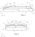
- the resistive network comprises a first and a second connection portion 36A, 38B connected to the gate conductive regions 22 and to the metal connection portions 38B, 38A, as described hereinafter and shown in Figures 3 and 4 , where, for simplicity, the gate insulating layer 21 is not represented.
- Figure 3 shows a peripheral edge portion (designated by 37) of the die 2, for example adjacent to the fourth side 2D.
- An insulation oxide annular portion 40A for example of silicon oxide, extends over the first surface 5A of the substrate 5 and is covered by a passivation layer 42, connected to the insulation layer 23.
- a delimitation region 41 having an opposite conductivity with respect to the substrate 5, here of P type, and having an annular shape, extends within the substrate 5, approximately underneath the inner edge of the insulation oxide annular portion 40A.
- the delimitation region 41 surrounds, in the substrate 5, an active area 44 (the limit whereof is represented schematically by a dashed line A); accommodating the conduction regions of the MOSFET device 1, including the source regions 25 and the body regions 10 (not visible in Figure 3 ).
- An implanted region 43 here of N + type and ring-shaped, forming a channel stopper, extends underneath the insulation oxide annular portion 40A, in proximity of the outer edge thereof and of the sides 5A-5D of the die 2, at a distance D from the delimitation region 41.
- the first connection portion 36A of polycrystalline silicon, extends as a ring over and along the inner edge of the insulation oxide annular portion 40A.
- the first connection portion 36A is here in direct electrical contact with a gate conductive region 22, without interruption, being obtained in the same layer.
- Figure 3 moreover shows the gate metal ring 38A, which extends above the insulation oxide annular portion 40A; the gate metal ring 38A crosses the passivation layer 42 and is here in direct electrical contact with the first connection portion 36A.
- Figure 4 shows the connection between the gate metal finger 38B and the gate conductive regions 22.
- an insulation oxide finger portion 40B formed by the same layer as the insulation oxide annular portion 40A, extends over the body 5, parallel to the first direction X, as far as and in contact with the sides of the insulation oxide annular portion 40A adjacent to the first and second sides 2A, 2B of the die 2.
- the insulation oxide finger portion 40B and the insulation oxide annular portion 40A form an edge insulation region 40.
- the second connection portion 36B extends over the insulation oxide finger portion 40B and also has an elongated shape in the first direction X.
- the second connection portion 36B has a width (in a direction parallel to the second direction Y) greater than the width (in the same direction) of the insulation oxide finger portion 40B and therefore extends also on the side of the insulation oxide finger portion 40B, where it is directly connected to the gate conductive regions 22. Moreover, it is directly connected, at its longitudinal ends, to the insulation oxide annular portion 40A.
- the insulation layer 23 covers the second connection portion 36B and has an opening 46 extending parallel to the first direction X, approximately throughout the length of the second connection portion 36B.
- the gate metal finger 38B extends through the opening 46 and is here in direct electrical contact with the second connection portion 36B.
- the insulation oxide finger portion 40B extends on a insulation finger region 45, of P type, formed in the body 5 and extending parallel to the first direction X, between two opposite sides of the delimitation region 41, with which it is in direct contact.
- the insulation oxide finger portion 40B overlies an inactive area 47 (also referred to as central edge area) that separates two active areas 44.
- the gate metal finger 38B and the gate metal ring 38A have the aim of reducing the voltage drop between the gate pad 35 and the gate conductive regions 22 due to the resistivity of the resistive network formed by the connection portions 36A, 36B.
- the gate metal finger 38B causes the source metallization to be divided into at least the two portions 33A, 33B (or even more, in devices that, due to their dimensions, have several gate metal fingers 38B). This limits the use of the MOSFET device 1 in power modules that have clips sintered or soldered on the die 2 or need particular, costly and/or cumbersome solutions for contacting the source metallization region 33.
- innovative reliability tests that verify the switching behaviour in high-humidity environments show that the gate metal ring 38A is a weak point of the device.
- the metal connection portions 38A, 38B cause a non-negligible encumbrance, both because of their dimensions and due to the minimum safety space to be provided between the portions 33A, 33B of the source metallization region 33 and the gate pad 35.
- the gate metal ring 38A is designed to maintain the distance D in Figure 3 between the channel-stopper region 43 and the delimitation region 41. Furthermore, as shown in Figure 4 , the distance D' between the active areas 44 (areas where the central edge area 47 and the gate metal finger 38B extend) cannot be used for the conduction of the MOSFET device 1 and represents a waste of area.
- US 2019/013311 discloses a power conversion device including a substrate of silicon carbide and having a gate conductive region and a gate connection region formed by a silicon layer and by a metal layer overlying the silicon layer.
- WO 2012/001837 discloses a power semiconductor device having an annular connection region.
- the aim of the present invention is to overcome the drawbacks of the prior art.
- Figures 5-9 show a MOSFET device 50, with vertical conduction, of silicon carbide.
- the MOSFET device 50 is formed in a die 52 having a generally parallelepipedal shape, with four lateral surfaces or sides 52A-52D and a top surface 52E.
- the die 52 has a first side 52A; a second side 52B, opposite the first side 52A; a third side 52C; and a fourth side 52D, opposite the third side 2C, wherein the third and fourth sides 52C, 52D are parallel to a first axis X of a Cartesian reference system XYZ, and the first and second sides 52A, 52B are parallel to a second axis Y of the Cartesian reference system XYZ.
- the MOSFET device 50 comprises a plurality of elementary cells (two shown in Figures 6 and 7 ) adjacent to each other and connected together in parallel. They thus share a source terminal S, a drain terminal D, and a gate terminal G.
- the die 52 comprises a substrate 55 of silicon carbide having a first surface 55A and a second surface 55B.
- the substrate 55 accommodates a drain region 57, a plurality of body regions 60, and a plurality of source regions 65, analogous to the respective same-name regions 7, 10 and 15 of Figure 1 and not described any further herein.
- a gate contact region 59 of conductive material such as a metal and/or a silicide, extends on the second surface 55B of the substrate 55, in direct electrical contact with the drain region 57, and forms the drain terminal D of the MOSFET device 50.
- a superficial portion 64 of the drain region 57 is comprised between two adjacent body regions 60.
- Each source region 65 laterally delimits, together with an adjacent superficial portion 64, a channel portion 75 of a respective body region 60.
- the MOSFET device 50 further comprises a plurality of insulated gate regions 70.
- the insulated gate regions 70 are each formed by a gate insulating region 71, in contact with the first surface 55A of substrate 55; a gate conductive region 72, directly overlying the gate insulating region 71; and a top insulation layer 73, surrounding and sealing, together with the gate insulating region 71, the gate conductive region 72.
- Each gate conductive region 72 is here formed by a gate semiconductor portion 76, typically of polycrystalline silicon, and a gate metal portion 77, directly overlying and in direct electrical contact with the gate semiconductor portion 76.
- the gate metal portion 77 is typically a metal silicide, for example tungsten, titanium, nickel, cobalt, or platinum silicide.
- the gate metal portion 77 has the same width (in the direction of the first axis X) as the gate semiconductor portion 76; in the embodiment of Figure 7 , the gate-metal region (designated by 77') has a smaller width than the gate semiconductor portion 76.
- each insulated gate region 70 extends on a respective superficial portion 64 of the drain region 57, on two channel regions 75 adjacent to the respective superficial portion 64, and partially on two source regions 65 adjacent to the respective channel regions 75.
- the gate conductive regions 72 are electrically connected in parallel to each other and to the gate terminal G of the MOSFET device 50, as explained below.
- the MOSFET device 50 further comprises a plurality of body contact regions 80 (hereinafter also referred to as P-well regions 80), analogous to the body contact regions 30 of Figure 1 .
- the P-well regions 80 and the source regions 65 are in direct electrical contact with a source metallization region 83, for example of metal and/or metal silicide.
- the source metallization region 83 is here formed by a single portion occupying most of the top surface 52E of the die 50 and forms also a pad for external connection of the MOSFET device 50.
- auxiliary source pads 84 and a gate pad 85 extend on the first surface 55A of the substrate 55.
- the auxiliary source pads 84, the gate pad 85, and the single source metallization region 83 are formed in a same layer and therefore have the same high thickness, for example comprised between 1 and 10 ⁇ m, so as to provide the desired current capability of the source terminal S.
- the source metallization region 83 may be formed by several separate portions, instead of a single portion. In any case, in the MOSFET device 50, the distance between them is not critical, and no gate metal finger (38B in Figure 1 ) is present, nor is a gate metal ring (38A in Figure 1 ).
- the gate pad 85 (here arranged in proximity of the first side 52A of the die 52, in a middle position) is connected to the gate conductive regions 72 (represented dashed in Figure 5 ) through an annular connection region 86, which extends in proximity of the periphery of the die 52 and has a widened portion forming a contact area 86A arranged underneath the gate pad 85.
- the annular connection region 86 is monolithic with the gate conductive regions 72, is formed by the same layers, and is obtained by the same process steps for forming the gate conductive regions 72, as described in detail hereinafter.
- annular connection region 86 is visible also in the cross-sections of Figures 8 and 9 , wherein, for simplicity, the gate insulating region 71 is not represented.
- Figure 8 shows a peripheral edge portion (designated by 87), of the die 52, for example adjacent to the second side 52B.
- An edge insulation region 90 extends on the first surface 55A of the substrate 55.
- the edge insulation region 90 here comprises an oxide layer 96 and a passivation layer 92 overlying the latter.
- the passivation layer 92 in proximity of the third and the fourth sides 52C, 52D of the die 52, prosecutes with the top insulation layer 73 of the insulated gate regions 70, which, in the cross-section of Figure 8 , is interrupted by the openings, where the source metallization 83 extends.
- a delimitation region 91 having a conductivity opposite that of the substrate 55, here of P type and annular shape, extends in the substrate 55 underneath the edge insulation region 90, in proximity of, but at a distance from, the inner edge of the latter.
- the delimitation region 91 surrounds, in the substrate 55, an active area 94 (whose limit is represented schematically by a dashed line B), accommodating the conduction regions of the MOSFET device 50, including the body regions 60 and the source regions 65.
- a channel-stopper region 93 here of N + type and annular shape, extends underneath the edge insulation region 90, in proximity of the sides 52A-52D of the die 52, at a distance D1 from the delimitation region 91, to balance the potential in the edge area.
- the annular connection region 86 extends in an annular way only along the inner edge of the edge insulation region 90 and does not have portions extending between active areas.
- the annular connection region 86 is formed monolithically with the gate conductive regions 72 as a stack of two layers.
- the annular connection region 86 comprises a semiconductor connection portion 88 and a metal connection portion 89, directly overlying and in direct electrical contact with the semiconductor connection portion 88.
- the material of the semiconductor connection region 88 is the same of the gate semiconductor portions 76 (typically of polycrystalline silicon), and the material of the metal connection portion 89 is the same of the gate metal portions 77 (typically a metal silicide, for example tungsten, titanium, nickel, cobalt, or platinum silicide).
- the stack of layers forming the gate semiconductor portions 76 and the annular connection region 86 forms a gate bias layer 95.
- the annular connection region 86 extends only to a minimal extent on the edge insulation region 90 and has a very small width, for example comprised between 10 and 50 ⁇ m.
- the delimitation region 91 has also a small width (in the first direction X, in the cross-section of Figure 8 ), for example comprised between 20 and 50 ⁇ m. In this way, the width of the peripheral edge portion 87 is reduced, and it is also possible to accordingly increase the dimensions of the active area 94, for same dimensions of the dice 2-52.
- the passivation layer 92/73 completely covers the metal connection portion 89 of the annular connection region 86 at the top, and there are no openings or conductive regions through the passivation layer 92/73, nor are there surface metal portions providing a direct electrical contact between the top surface of the annular connection region 86 and the gate metallization 85. Biasing of the annular connection region 86 occurs in fact only at its portions contiguous with the contact area 86A.
- the MOSFET device 50 thus has a wide active area 94 and therefore effectively exploits the area of the die 52.
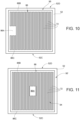
- Figures 10 and 11 show two possible layouts of the gate bias layer 95.
- Figure 10 shows the layout of the gate bias layer 95 corresponding to what is shown in Figure 5 , with the contact area 86A arranged peripherally.
- the annular connection region 86 has a first and a second branch 86B, 86C, which extend along and in proximity of two opposite sides of the body 52 (and precisely, in the embodiment shown in Figure 10 , along the third and fourth sides 52C, 52D of the die 52), and the gate conductive regions 72 extend continuously between the first and second branches 86B, 86C of the annular connection region 86.
- Figure 11 shows a different layout of the gate bias layer, here designated by 95'.
- the gate conductive regions 72 extend continuously between the first and second branches 86B, 86C of the annular connection region 86.
- the gate conductive regions 72 arranged most centrally have a widened central portion which is common to different gate conductive regions 72 and forms a contact area 86A' on which the gate pad 85 extends.
- biasing of the annular connection region 86 occurs only through the gate conductive regions 72 that connect the annular connection region 86 to the contact area 86A'.
- the position of the gate pad 85 and therefore of the contact area 86A, 86A' can be chosen with high freedom, according to the applications and possible customer desires.
- the MOSFET device 52 of Figures 5 , 6 and 8-11 may be manufactured by depositing/forming a silicide layer before or after defining the gate semiconductor portions 76 of the gate conductive regions 72.
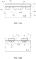
- Figure 12A shows a wafer 100 of silicon carbide (for example of a 3C-SiC, 4H-SiC or 6H-SiC type) intended to form, after dicing, the die 52 of Figure 6 .
- the source regions 65, the body regions 60, and the P-well regions 80 are already formed within the substrate 55, as likewise the various edge regions (including the delimitation region 91 and the channel-stopper region 93 of Figure 8 ), here not visible.
- a gate insulating layer 101, a gate conductive layer 102, and a silicide layer 103 have already been deposited, in sequence, on the first surface 55A of the substrate 55.
- the gate insulating layer 101 is, for example, silicon oxide and is intended to form the gate insulating regions 71.
- the gate conductive layer 102 is typically polycrystalline silicon and is designed to form the gate semiconductor portions 76 of the gate conductive regions 72 and the semiconductor connection portion 88.
- the silicide layer 103 is, for example, tungsten silicide (WSi 2 ) and is intended to form the gate metal portions 77 and the metal connection portion 89 ( Figures 6 and 8 ).
- the silicide layer 103, the gate conductive layer 102, and the gate insulating layer 101 are defined in a known way, by a photolithographic process and using the same etching mask ( Figure 12B ).
- the gate conductive regions 72 ( Figures 6 and 12B ), the annular connection region 86 ( Figure 8 ) and the gate insulating regions 7 are formed. Furthermore, the gate metal portions 77 and the gate semiconductor portions 76 are self-aligned to each other, as likewise the metal connection portion 89 and the semiconductor connection portion 88.
- Figures 13A-13C show steps of a different embodiment of a manufacturing process of the MOSFET device 50 of Figures 5 , 6 and 8-11 .
- Figure 13A shows a portion of wafer 100.
- the source regions 65, the body regions 60, and the P-well regions 80, as well as the various edge regions, have already been formed in the substrate 55.
- the gate insulating layer 101 has already been deposited on the first surface 55A of the substrate 55, and the gate semiconductor portions 76 of the gate conductive regions 72, as well as the semiconductor connection portion 88, have already been formed, for example by depositing and photolithographically defining a polycrystalline silicon layer.
- a sacrificial layer 105 for example, of silicon oxide, is deposited on the gate semiconductor portions 76 and on the gate insulating layer 101, where exposed.
- the sacrificial layer 105 is etched to form spacers 106 (spacer etching).
- spacer etching is of a non-masked, dry, directional type (plasma etching). Due to the etch anisotropy, the horizontal portions of the sacrificial layer 105 are removed, and the spacers 106 are formed on the vertical walls of the gate semiconductor portions 76. In this step, also the portions of the gate insulating layer 101 not covered by the gate semiconductor portions 76 and by the spacers 106, on the source regions 65, are eliminated, forming the gate insulating regions 71.
- a metal layer for example, titanium or nickel is deposited by sputtering and reacts with the polycrystalline silicon of the gate semiconductor portions 76 and (in a way not shown) of the semiconductor connection portion 88 ( Figure 8 ).
- a first annealing is carried out at a low temperature, for example comprised 600°C and 1000°C.
- the non-reacted metal material (for example, on the spacers 106) is removed, and a second annealing is carried out at a higher temperature, for example comprised between 800°C and 1100°C.
- the gate metal portions 77 are self-aligned with the respective gate semiconductor portions 76, and the metal connection portion 89 is self-aligned with the semiconductor connection portion 88.
- a thin silicide layer may form on the exposed portions of the substrate 55, in particular on the source regions 65 and on the P-well regions 80; these portions may be removed by an appropriate etch or left, according to the specific process.
- the process proceeds with the usual steps for forming the top insulation layer 73, the passivation layer 92, and the metallizations 83-85.
- Figures 14A-14B show steps of an embodiment of a process for manufacturing the MOSFET device 50 of Figures 5 , 7 and 8-11 .
- Figure 14A shows a wafer 100' after performing the manufacturing steps already described for Figure 13A .
- the source regions 65, the body regions 60, and the P-well regions 80, as well as the various edge regions, have already been formed in the substrate 55.
- the gate insulating layer 101 has already been deposited on the first surface 55A of the substrate 55.
- the gate semiconductor portions 76 of the gate conductive regions 72, as well as the semiconductor connection portion 88 (not visible in Figure 14A ) have already been formed, for example by depositing and photolithographically defining a polycrystalline silicon layer.
- a sacrificial layer 115 for example, silicon oxide, has been deposited on the gate semiconductor portions 76 and on the gate insulating layer 101, where exposed.
- a gate contact mask (not shown) is formed on the sacrificial layer 115, and the sacrificial layer 115 is selectively removed on the gate semiconductor portions 76 and on the semiconductor connection portion 88 (not visible in Figure 14B ).
- a metal layer for example, of titanium, cobalt, or platinum is deposited by sputtering and caused to react with the polycrystalline silicon of the gate semiconductor portions 76 and (in a way not shown) of the semiconductor connection portion 88 ( Figure 8 ).
- a first annealing at low temperature for example comprised between 600°C and 1000°C, is carried out.
- the non-reacted metal material (on the masking portions 115') is removed, and a second annealing is carried out at a higher temperature, for example comprised between 800°C and 1100°C.
- the remaining, non-reacted, portions of the sacrificial layer 105 are removed, and the further steps for forming the top insulation layer 73, the passivation layer 92, and the metallizations 83-85 are carried out.
- the MOSFET device 50 thus formed has many advantages.
- the MOSFET device 50 has an improved gate resistance Rg, since it has no waste of area due to the metal connection portions.
- the MOSFET device 50 moreover has excellent robustness and may be used also in high-current and/or high-voltage applications. For instance, it is able to work at voltages up to 10 kV or currents up to 500 A.
- the MOSFET device 50 has improved reliability because the structure is simplified and the polysilicon of the gate semiconductor portions 76 does not require a particular doping. Consequently, there is no precipitation of dopant (typically, phosphorus) from the gate conductive regions 72 into the gate insulating region 71. In this way, the latter region, typically of oxide, presents a high reliability.
- dopant typically, phosphorus
- the external contact structures (clips) that are brought into contact with the source metallization 83 during assembly and packaging of the MOSFET device 50 may be simplified, reducing costs and improving the current conduction reliability.
- the silicide layer 103 may be obtained by reacting a metal layer deposited on the gate conductive layer 102.
Landscapes
- Electrodes Of Semiconductors (AREA)
- Engineering & Computer Science (AREA)
- Manufacturing & Machinery (AREA)
- Insulated Gate Type Field-Effect Transistor (AREA)
- Junction Field-Effect Transistors (AREA)
Claims (13)
- MOSFET-Vorrichtung (50) mit vertikaler Leitung, umfassend:
einen Körper (55) aus Siliziumkarbid, der eine erste und eine zweite Seite (52A, 52B) und eine Umfangszone (87) aufweist, wobei der Körper beherbergt:einen ersten Stromleitungsbereich (57) eines ersten Leitfähigkeitstyps, der sich im Körper (55) von der zweiten Seite (55B) aus erstreckt und einen oberflächlichen Abschnitt (64) aufweist, der der ersten Seite (55A) zugewandt ist;einen Körperbereich (60) eines zweiten Leitfähigkeitstyps, der sich im Körper von der ersten Seite (55A) aus erstreckt; undeinen zweiten Stromleitungsbereich (65) des ersten Leitfähigkeitstyps, der sich von der ersten Seite (55A) des Körpers aus zur Innenseite des Körperbereichs (60) erstreckt, wobei der zweite Stromleitungsbereich (65) im Körperbereich (60) zusammen mit dem oberflächlichen Abschnitt (64) einen Kanalabschnitt (75) begrenzt;einen isolierten Gate-Bereich (70), der sich auf der ersten Seite (55A) des Körpers (55) erstreckt und über dem Kanalabschnitt (75) liegt, wobei der isolierte Gate-Bereich (70) einen leitfähigen Gate-Bereich (72) umfasst; undeine Oberflächen-Randstruktur (90), die einen isolierten Randbereich (96) umfasst, der sich auf der ersten Seite (55A) des Körpers (55) in der Umfangszone (87) des Körpers erstreckt,einen Verbindungsbereich (86) aus leitfähigem Material, der sich ringförmig nur entlang des inneren Randes des Randisolierbereichs erstreckt und keine Abschnitte aufweist, die sich zwischen aktiven Flächen erstrecken,wobei:der leitfähige Gate-Bereich (72) und der ringförmige Verbindungsbereich (86) von einer Gate-Vorspannungsschicht (95) gebildet werden, die eine Siliziumschicht und eine über der Siliziumschicht liegende Metallsilizidschicht beinhaltet,der leitfähige Gate-Bereich (72) einen Gate-Halbleiterabschnitt (76), der von der Siliziumschicht gebildet wird, und einen Gate-Metallabschnitt (77) umfasst, der von der Metallsilizidschicht gebildet wird,der ringförmige Verbindungsbereich (86) einen Halbleiterverbindungsabschnitt (88), der von der Siliziumschicht gebildet wird, und einen Metallverbindungsabschnitt (89) umfasst, der von der Metallsilizidschicht gebildet wird, unddie Oberflächen-Randstruktur (90) eine Passivierungsschicht (92) umfasst, die den Metallverbindungsabschnitt (89) des ringförmigen Verbindungsbereichs (86) vollständig bedeckt. - MOSFET-Vorrichtung mit vertikaler Leitung nach Anspruch 1, wobei die Siliziumschicht eine polykristalline Schicht ist.
- MOSFET-Vorrichtung mit vertikaler Leitung nach Anspruch 1 oder Anspruch 2, wobei die Metallsilizidschicht ausgewählt ist aus Wolfram-, Titan-, Nickel-, Kobalt- oder Platinsilizid.
- MOSFET-Vorrichtung mit vertikaler Leitung nach einem der vorstehenden Ansprüche, wobei der Gate-Halbleiterabschnitt (76) eine erste Breite aufweist, der Gate-Metallabschnitt (77) eine zweite Breite aufweist, der Halbleiterverbindungsabschnitt (88) eine dritte Breite aufweist und der Metallverbindungsabschnitt (89) eine vierte Breite aufweist, wobei die erste Breite gleich der zweiten Breite ist und die dritte Breite gleich der vierten Breite ist.
- MOSFET-Vorrichtung mit vertikaler Leitung nach einem der Ansprüche 1-3, wobei der Gate-Halbleiterabschnitt (76) eine erste Breite aufweist, der Gate-Metallabschnitt (77) eine zweite Breite aufweist, der Halbleiterverbindungsabschnitt (88) eine dritte Breite aufweist und der Metallverbindungsabschnitt (89) eine vierte Breite aufweist, wobei die erste Breite größer ist als die zweite Breite und die dritte Breite größer ist als die vierte Breite.
- MOSFET-Vorrichtung mit vertikaler Leitung nach einem der vorstehenden Ansprüche, wobei die erste Seite (55A) des Körpers (55) eine Fläche und einen zentralen Abschnitt aufweist, wobei die MOSFET-Vorrichtung mit vertikaler Leitung (50) weiter einen Leitungskontakt-Metallbereich (83) umfasst, der sich auf der ersten Seite (55A) des Körpers (55) in direktem elektrischen Kontakt mit dem zweiten Stromleitungsbereich (65) erstreckt, wobei der Leitungskontakt-Metallbereich (83) einen einzelnen Kontaktabschnitt umfasst, der den Großteil der Fläche der ersten Seite (55A) bedeckt und sich ohne Unterbrechung über den zentralen Abschnitt der ersten Seite (55A) erstreckt.
- MOSFET-Vorrichtung mit vertikaler Leitung nach einem der vorstehenden Ansprüche, wobei der Körper (55) zwei gegenüberliegende seitliche Oberflächen (52C, 52D) aufweist, der ringförmige Verbindungsbereich (86) einen ersten und einen zweiten Schenkel aufweist, die sich in der Nähe der gegenüberliegenden seitlichen Oberflächen (52C, 52D) des Körpers (55) erstrecken, und der leitfähige Gate-Bereich (72) sich mit Durchgängigkeit zwischen dem ersten und dem zweiten Schenkel (86A, 86B) des ringförmigen Verbindungsbereichs (86) erstreckt.
- Prozess zum Herstellen einer MOSFET-Vorrichtung mit vertikaler Leitung nach einem der Ansprüche 1-7, umfassend: Bilden, in einem Körper (55) aus Siliziumkarbid, der eine erste und eine zweite Seite (55A, 55B) und eine Umfangszone (87) aufweist und einen ersten Stromleitungsbereich (57) eines ersten Leitfähigkeitstyps beherbergt, welcher sich in dem Körper von der zweiten Seite aus erstreckt und einen oberflächlichen Abschnitt (64) aufweist, der der ersten Seite zugewandt ist, eines Körperbereichs (60) eines zweiten Leitfähigkeitstyps, der sich im Körper von der zweiten Seite aus erstreckt;Bilden, im Körperbereich, eines zweiten Stromleitungsbereichs (65) des ersten Leitfähigkeitstyps, der sich von der ersten Seite des Körpers aus erstreckt, wobei der zweite Stromleitungsbereich im Körperbereich zusammen mit dem oberflächlichen Abschnitt einen Kanalabschnitt (75) begrenzt;Bilden eines isolierten Gate-Bereichs (70) auf der ersten Seite des Körpers an einer Position, die über dem Kanalabschnitt liegt, wobei der isolierte Gate-Bereich einen leitfähigen Gate-Bereich (72) umfasst; undBilden einer Oberflächen-Randstruktur (90), die einen isolierten Randbereich (96) umfasst, der sich auf der ersten Seite des Körpers an der Umfangszone des Körpers erstreckt,Bilden eines Verbindungsbereichs (86) aus leitfähigem Material, der sich ringförmig nur entlang des inneren Randes des Randisolierbereichs erstreckt und keine Abschnitte aufweist, die sich zwischen aktiven Flächen erstrecken,wobei das Bilden des leitfähigen Gate-Bereichs (72) und das Bilden des ringförmigen Verbindungsbereichs (86) das Bilden einer Gate-Vorspannungsschicht (95) umfasst, die eine Siliziumschicht und eine Metallsilizidschicht beinhaltet, die über der Siliziumschicht liegt, undder ringförmige Verbindungsbereich (86) einen Halbleiterverbindungsabschnitt (88), der von der Siliziumschicht (102) gebildet wird, und einen Metallverbindungsabschnitt (89) umfasst, der von der Metallsilizidschicht gebildet wird, wobei der Prozess weiter das Abscheiden einer Passivierungsschicht (92) umfasst, die den Metallverbindungsabschnitt (89) des ringförmigen Verbindungsbereichs (86) vollständig bedeckt.
- Prozess nach dem vorstehenden Anspruch, wobei das Bilden einer Gate-Vorspannungsschicht (95) umfasst:Abscheiden der Siliziumschicht (102) auf der ersten Seite (55A) des Körpers (55);Bilden der Metallsilizidschicht (103) auf der Siliziumschicht; undphotolithographisches Definieren der Siliziumschicht und der Metallsilizidschicht, wodurch der leitfähige Gate-Bereich (72) und der ringförmige Verbindungsbereich (86) gebildet werden.
- Prozess nach Anspruch 8, wobei das Bilden einer Gate-Vorspannungsschicht (95) umfasst:Abscheiden der Siliziumschicht (102) auf der ersten Seite des Körpers;photolithographisches Definieren der Siliziumschicht, um einen Gate-Halbleiterabschnitt (76) und einen Halbleiterverbindungsabschnitt (88) zu bilden, wobei der Gate-Halbleiterabschnitt (76) und der Halbleiterverbindungsabschnitt (88) seitliche Oberflächen aufweisen;Bilden von Abstandshaltern (106) an den seitlichen Oberflächen;Abscheiden einer Metallschicht in direktem Kontakt mit dem Gate-Halbleiterabschnitt (76) und mit dem Halbleiterverbindungsabschnitt (88); undUmsetzen der Metallschicht, wodurch ein Gate-Metallabschnitt (77) in Kontakt mit dem Gate-Halbleiterabschnitt (76) und ein Metallverbindungsabschnitt in Kontakt mit dem Halbleiterverbindungsabschnitt (88) erhalten werden.
- Prozess nach Anspruch 8, wobei das Bilden einer Gate-Vorspannungsschicht (95) umfasst:Abscheiden der Siliziumschicht (102) auf der ersten Seite des Körpers;photolithographisches Definieren der Siliziumschicht, um einen Gate-Halbleiterabschnitt (76) und einen Halbleiterverbindungsabschnitt (88) zu bilden, wobei der Gate-Halbleiterabschnitt (76) und der Halbleiterverbindungsabschnitt (88) seitliche Oberflächen und Längsränder aufweisen;Bilden von Maskierungsabschnitten (115'), die die seitlichen Oberflächen und die Längsränder der Gate-Halbleiterabschnitte (76) und des Halbleiterverbindungsabschnitts (88) bedecken;Abscheiden einer Metallreaktionsschicht in direktem Kontakt mit dem Gate-Halbleiterabschnitt (76) und mit dem Halbleiterverbindungsabschnitt (88) dort, wo sie von den Maskierungsabschnitten (115') freigelegt werden; undUmsetzen der Metallreaktionsschicht, wodurch ein Gate-Metallabschnitt (77) in Kontakt mit dem Gate-Halbleiterabschnitt (76) und ein Metallverbindungsabschnitt in Kontakt mit dem Halbleiterverbindungsabschnitt (88) erhalten werden.
- Prozess nach Anspruch 10 oder 11, wobei das Umsetzen der Metallreaktionsschicht das Durchführen eines Glühens umfasst, und weiter das Entfernen von nicht umgesetzten Abschnitten der Metallreaktionsschicht umfassend.
- Prozess nach einem der Ansprüche 8-12, wobei die Siliziumschicht (102) polykristallines Silizium ist und die Metallreaktionsschicht aus Wolfram, Titan, Nickel, Kobalt und Platin ausgewählt ist.
Applications Claiming Priority (1)
| Application Number | Priority Date | Filing Date | Title |
|---|---|---|---|
| IT102021000003653A IT202100003653A1 (it) | 2021-02-17 | 2021-02-17 | Dispositivo mosfet di carburo di silicio, a conduzione verticale, avente struttura di polarizzazione di porta perfezionata e relativo procedimento di fabbricazione |
Publications (3)
| Publication Number | Publication Date |
|---|---|
| EP4047664A1 EP4047664A1 (de) | 2022-08-24 |
| EP4047664B1 true EP4047664B1 (de) | 2025-01-29 |
| EP4047664C0 EP4047664C0 (de) | 2025-01-29 |
Family
ID=75660261
Family Applications (1)
| Application Number | Title | Priority Date | Filing Date |
|---|---|---|---|
| EP22155166.6A Active EP4047664B1 (de) | 2021-02-17 | 2022-02-04 | Siliziumkarbid-mosfet-vorrichtung mit vertikaler leitung mit verbesserter gate-vorspannungsstruktur und verfahren zur herstellung davon |
Country Status (5)
| Country | Link |
|---|---|
| US (1) | US12249634B2 (de) |
| EP (1) | EP4047664B1 (de) |
| JP (1) | JP7810569B2 (de) |
| CN (2) | CN217847965U (de) |
| IT (1) | IT202100003653A1 (de) |
Families Citing this family (1)
| Publication number | Priority date | Publication date | Assignee | Title |
|---|---|---|---|---|
| IT202100003653A1 (it) * | 2021-02-17 | 2022-08-17 | St Microelectronics Srl | Dispositivo mosfet di carburo di silicio, a conduzione verticale, avente struttura di polarizzazione di porta perfezionata e relativo procedimento di fabbricazione |
Family Cites Families (17)
| Publication number | Priority date | Publication date | Assignee | Title |
|---|---|---|---|---|
| CN101542740B (zh) * | 2007-02-14 | 2011-01-12 | 松下电器产业株式会社 | 半导体装置及其制造方法 |
| US7829416B2 (en) | 2007-08-07 | 2010-11-09 | Panasonic Corporation | Silicon carbide semiconductor device and method for producing the same |
| TW200937635A (en) * | 2008-02-21 | 2009-09-01 | Amic Technology Corp | Metal-oxide-semiconductor transistor device and related manufacturing method |
| JP5370480B2 (ja) * | 2009-04-30 | 2013-12-18 | 三菱電機株式会社 | 半導体装置及びその製造方法 |
| WO2011048800A1 (ja) * | 2009-10-23 | 2011-04-28 | パナソニック株式会社 | 半導体装置およびその製造方法 |
| JP5692227B2 (ja) * | 2010-06-30 | 2015-04-01 | 三菱電機株式会社 | 電力用半導体装置 |
| JP5654818B2 (ja) * | 2010-09-27 | 2015-01-14 | ルネサスエレクトロニクス株式会社 | パワー系半導体装置の製造方法 |
| JP2013004636A (ja) * | 2011-06-15 | 2013-01-07 | Sumitomo Electric Ind Ltd | 炭化珪素半導体装置およびその製造方法 |
| JP6218423B2 (ja) * | 2013-04-25 | 2017-10-25 | 三菱電機株式会社 | 炭化珪素半導体装置およびその製造方法 |
| JP6256659B2 (ja) * | 2015-04-20 | 2018-01-10 | 富士電機株式会社 | 半導体装置 |
| JP2017028219A (ja) | 2015-07-28 | 2017-02-02 | 三菱電機株式会社 | 炭化珪素半導体装置およびその製造方法 |
| JP7280666B2 (ja) * | 2017-05-17 | 2023-05-24 | ローム株式会社 | 半導体装置およびその製造方法 |
| US10403623B2 (en) * | 2017-07-06 | 2019-09-03 | General Electric Company | Gate networks having positive temperature coefficients of resistance (PTC) for semiconductor power conversion devices |
| US12094876B2 (en) * | 2020-04-30 | 2024-09-17 | Wolfspeed, Inc. | Conduction enhancement layers for electrical contact regions in power devices |
| IT202100003653A1 (it) * | 2021-02-17 | 2022-08-17 | St Microelectronics Srl | Dispositivo mosfet di carburo di silicio, a conduzione verticale, avente struttura di polarizzazione di porta perfezionata e relativo procedimento di fabbricazione |
| JP2023046089A (ja) * | 2021-09-22 | 2023-04-03 | 富士フイルムビジネスイノベーション株式会社 | 情報処理装置、情報処理システム、及び情報処理プログラム |
| IT202200014566A1 (it) * | 2022-07-11 | 2024-01-11 | St Microelectronics Srl | Dispositivo mosfet di potenza con struttura di porta isolata migliorata e relativo processo di fabbricazione |
-
2021
- 2021-02-17 IT IT102021000003653A patent/IT202100003653A1/it unknown
-
2022
- 2022-02-04 EP EP22155166.6A patent/EP4047664B1/de active Active
- 2022-02-10 US US17/669,239 patent/US12249634B2/en active Active
- 2022-02-14 JP JP2022020511A patent/JP7810569B2/ja active Active
- 2022-02-16 CN CN202220309168.0U patent/CN217847965U/zh active Active
- 2022-02-16 CN CN202210140503.3A patent/CN114944428A/zh active Pending
Also Published As
| Publication number | Publication date |
|---|---|
| JP2022125984A (ja) | 2022-08-29 |
| JP7810569B2 (ja) | 2026-02-03 |
| EP4047664A1 (de) | 2022-08-24 |
| CN217847965U (zh) | 2022-11-18 |
| US12249634B2 (en) | 2025-03-11 |
| IT202100003653A1 (it) | 2022-08-17 |
| EP4047664C0 (de) | 2025-01-29 |
| US20220262913A1 (en) | 2022-08-18 |
| CN114944428A (zh) | 2022-08-26 |
Similar Documents
| Publication | Publication Date | Title |
|---|---|---|
| US4399449A (en) | Composite metal and polysilicon field plate structure for high voltage semiconductor devices | |
| US4412242A (en) | Planar structure for high voltage semiconductor devices with gaps in glassy layer over high field regions | |
| EP1128443B1 (de) | Feldeffekt-halbleiterbauelement und verfahren zu dessen herstellung | |
| JP2585331B2 (ja) | 高耐圧プレーナ素子 | |
| EP1850385B1 (de) | Halbleiterbauelement und Herstellungsverfahren dafür | |
| US8035112B1 (en) | SIC power DMOSFET with self-aligned source contact | |
| KR102789257B1 (ko) | 분할-게이트 트렌치 mosfet | |
| US11489047B2 (en) | Semiconductor device and method of manufacturing the same | |
| JP5397289B2 (ja) | 電界効果トランジスタ | |
| CN102694011A (zh) | 半导体器件 | |
| WO2001091190A1 (en) | A semiconductor device | |
| JP7674656B2 (ja) | 炭化ケイ素半導体装置 | |
| EP4047664B1 (de) | Siliziumkarbid-mosfet-vorrichtung mit vertikaler leitung mit verbesserter gate-vorspannungsstruktur und verfahren zur herstellung davon | |
| US8384137B2 (en) | Semiconductor device | |
| US12604491B2 (en) | Semiconductor device including auxiliary electrode that is electrically connected to a control electrode via a second electrode layer | |
| JP6771433B2 (ja) | 半導体装置 | |
| CN118507521A (zh) | 功率半导体器件 | |
| JP2019067902A (ja) | 半導体装置の製造方法 | |
| US20240136348A1 (en) | Semiconductor device and manufacturing method of forming the same | |
| US20240030344A1 (en) | Semiconductor device | |
| US20250040207A1 (en) | Semiconductor device | |
| JP2002537657A (ja) | 絶縁ゲート電界効果半導体デバイス | |
| JP2022012503A (ja) | 半導体装置 | |
| WO2024202941A1 (ja) | 半導体装置 | |
| CN118969793A (zh) | 半导体器件 |
Legal Events
| Date | Code | Title | Description |
|---|---|---|---|
| PUAI | Public reference made under article 153(3) epc to a published international application that has entered the european phase |
Free format text: ORIGINAL CODE: 0009012 |
|
| STAA | Information on the status of an ep patent application or granted ep patent |
Free format text: STATUS: THE APPLICATION HAS BEEN PUBLISHED |
|
| AK | Designated contracting states |
Kind code of ref document: A1 Designated state(s): AL AT BE BG CH CY CZ DE DK EE ES FI FR GB GR HR HU IE IS IT LI LT LU LV MC MK MT NL NO PL PT RO RS SE SI SK SM TR |
|
| STAA | Information on the status of an ep patent application or granted ep patent |
Free format text: STATUS: REQUEST FOR EXAMINATION WAS MADE |
|
| 17P | Request for examination filed |
Effective date: 20230215 |
|
| RBV | Designated contracting states (corrected) |
Designated state(s): AL AT BE BG CH CY CZ DE DK EE ES FI FR GB GR HR HU IE IS IT LI LT LU LV MC MK MT NL NO PL PT RO RS SE SI SK SM TR |
|
| STAA | Information on the status of an ep patent application or granted ep patent |
Free format text: STATUS: EXAMINATION IS IN PROGRESS |
|
| REG | Reference to a national code |
Ref country code: DE Ref legal event code: R079 Free format text: PREVIOUS MAIN CLASS: H01L0029490000 Ipc: H01L0029423000 Ref document number: 602022009891 Country of ref document: DE |
|
| GRAP | Despatch of communication of intention to grant a patent |
Free format text: ORIGINAL CODE: EPIDOSNIGR1 |
|
| STAA | Information on the status of an ep patent application or granted ep patent |
Free format text: STATUS: GRANT OF PATENT IS INTENDED |
|
| 17Q | First examination report despatched |
Effective date: 20240807 |
|
| RIC1 | Information provided on ipc code assigned before grant |
Ipc: H01L 29/49 20060101ALI20240813BHEP Ipc: H01L 21/336 20060101ALI20240813BHEP Ipc: H01L 29/78 20060101ALI20240813BHEP Ipc: H01L 29/423 20060101AFI20240813BHEP |
|
| INTG | Intention to grant announced |
Effective date: 20240902 |
|
| RIN1 | Information on inventor provided before grant (corrected) |
Inventor name: CAMALLERI, CATENO MARCO Inventor name: GUARNERA, ALFIO Inventor name: SAGGIO, MARIO GIUSEPPE |
|
| GRAS | Grant fee paid |
Free format text: ORIGINAL CODE: EPIDOSNIGR3 |
|
| GRAA | (expected) grant |
Free format text: ORIGINAL CODE: 0009210 |
|
| STAA | Information on the status of an ep patent application or granted ep patent |
Free format text: STATUS: THE PATENT HAS BEEN GRANTED |
|
| AK | Designated contracting states |
Kind code of ref document: B1 Designated state(s): AL AT BE BG CH CY CZ DE DK EE ES FI FR GB GR HR HU IE IS IT LI LT LU LV MC MK MT NL NO PL PT RO RS SE SI SK SM TR |
|
| REG | Reference to a national code |
Ref country code: GB Ref legal event code: FG4D |
|
| REG | Reference to a national code |
Ref country code: CH Ref legal event code: EP |
|
| REG | Reference to a national code |
Ref country code: DE Ref legal event code: R096 Ref document number: 602022009891 Country of ref document: DE |
|
| REG | Reference to a national code |
Ref country code: IE Ref legal event code: FG4D |
|
| U01 | Request for unitary effect filed |
Effective date: 20250129 |
|
| U07 | Unitary effect registered |
Designated state(s): AT BE BG DE DK EE FI FR IT LT LU LV MT NL PT RO SE SI Effective date: 20250205 |
|
| U20 | Renewal fee for the european patent with unitary effect paid |
Year of fee payment: 4 Effective date: 20250218 |
|
| PG25 | Lapsed in a contracting state [announced via postgrant information from national office to epo] |
Ref country code: RS Free format text: LAPSE BECAUSE OF FAILURE TO SUBMIT A TRANSLATION OF THE DESCRIPTION OR TO PAY THE FEE WITHIN THE PRESCRIBED TIME-LIMIT Effective date: 20250429 |
|
| PG25 | Lapsed in a contracting state [announced via postgrant information from national office to epo] |
Ref country code: PL Free format text: LAPSE BECAUSE OF FAILURE TO SUBMIT A TRANSLATION OF THE DESCRIPTION OR TO PAY THE FEE WITHIN THE PRESCRIBED TIME-LIMIT Effective date: 20250129 |
|
| PG25 | Lapsed in a contracting state [announced via postgrant information from national office to epo] |
Ref country code: ES Free format text: LAPSE BECAUSE OF FAILURE TO SUBMIT A TRANSLATION OF THE DESCRIPTION OR TO PAY THE FEE WITHIN THE PRESCRIBED TIME-LIMIT Effective date: 20250129 |
|
| PG25 | Lapsed in a contracting state [announced via postgrant information from national office to epo] |
Ref country code: IS Free format text: LAPSE BECAUSE OF FAILURE TO SUBMIT A TRANSLATION OF THE DESCRIPTION OR TO PAY THE FEE WITHIN THE PRESCRIBED TIME-LIMIT Effective date: 20250529 Ref country code: NO Free format text: LAPSE BECAUSE OF FAILURE TO SUBMIT A TRANSLATION OF THE DESCRIPTION OR TO PAY THE FEE WITHIN THE PRESCRIBED TIME-LIMIT Effective date: 20250429 |
|
| PG25 | Lapsed in a contracting state [announced via postgrant information from national office to epo] |
Ref country code: HR Free format text: LAPSE BECAUSE OF FAILURE TO SUBMIT A TRANSLATION OF THE DESCRIPTION OR TO PAY THE FEE WITHIN THE PRESCRIBED TIME-LIMIT Effective date: 20250129 |
|
| PG25 | Lapsed in a contracting state [announced via postgrant information from national office to epo] |
Ref country code: GR Free format text: LAPSE BECAUSE OF FAILURE TO SUBMIT A TRANSLATION OF THE DESCRIPTION OR TO PAY THE FEE WITHIN THE PRESCRIBED TIME-LIMIT Effective date: 20250430 |
|
| REG | Reference to a national code |
Ref country code: CH Ref legal event code: PL |
|
| PG25 | Lapsed in a contracting state [announced via postgrant information from national office to epo] |
Ref country code: SM Free format text: LAPSE BECAUSE OF FAILURE TO SUBMIT A TRANSLATION OF THE DESCRIPTION OR TO PAY THE FEE WITHIN THE PRESCRIBED TIME-LIMIT Effective date: 20250129 |
|
| PG25 | Lapsed in a contracting state [announced via postgrant information from national office to epo] |
Ref country code: MC Free format text: LAPSE BECAUSE OF FAILURE TO SUBMIT A TRANSLATION OF THE DESCRIPTION OR TO PAY THE FEE WITHIN THE PRESCRIBED TIME-LIMIT Effective date: 20250129 |
|
| PG25 | Lapsed in a contracting state [announced via postgrant information from national office to epo] |
Ref country code: CH Free format text: LAPSE BECAUSE OF NON-PAYMENT OF DUE FEES Effective date: 20250228 |
|
| PG25 | Lapsed in a contracting state [announced via postgrant information from national office to epo] |
Ref country code: CZ Free format text: LAPSE BECAUSE OF FAILURE TO SUBMIT A TRANSLATION OF THE DESCRIPTION OR TO PAY THE FEE WITHIN THE PRESCRIBED TIME-LIMIT Effective date: 20250129 |
|
| PG25 | Lapsed in a contracting state [announced via postgrant information from national office to epo] |
Ref country code: SK Free format text: LAPSE BECAUSE OF FAILURE TO SUBMIT A TRANSLATION OF THE DESCRIPTION OR TO PAY THE FEE WITHIN THE PRESCRIBED TIME-LIMIT Effective date: 20250129 |
|
| PLBE | No opposition filed within time limit |
Free format text: ORIGINAL CODE: 0009261 |
|
| STAA | Information on the status of an ep patent application or granted ep patent |
Free format text: STATUS: NO OPPOSITION FILED WITHIN TIME LIMIT |
|
| 26N | No opposition filed |
Effective date: 20251030 |
|
| PG25 | Lapsed in a contracting state [announced via postgrant information from national office to epo] |
Ref country code: IE Free format text: LAPSE BECAUSE OF NON-PAYMENT OF DUE FEES Effective date: 20250204 |
|
| U20 | Renewal fee for the european patent with unitary effect paid |
Year of fee payment: 5 Effective date: 20260121 |