EP4042233B1 - Mixed-reality-kombinierer - Google Patents
Mixed-reality-kombinierer Download PDFInfo
- Publication number
- EP4042233B1 EP4042233B1 EP21761635.8A EP21761635A EP4042233B1 EP 4042233 B1 EP4042233 B1 EP 4042233B1 EP 21761635 A EP21761635 A EP 21761635A EP 4042233 B1 EP4042233 B1 EP 4042233B1
- Authority
- EP
- European Patent Office
- Prior art keywords
- waveguide
- light
- facets
- reflectivity
- range
- Prior art date
- Legal status (The legal status is an assumption and is not a legal conclusion. Google has not performed a legal analysis and makes no representation as to the accuracy of the status listed.)
- Active
Links
Images


Classifications
-
- G—PHYSICS
- G02—OPTICS
- G02B—OPTICAL ELEMENTS, SYSTEMS OR APPARATUS
- G02B27/00—Optical systems or apparatus not provided for by any of the groups G02B1/00 - G02B26/00, G02B30/00
- G02B27/0081—Optical systems or apparatus not provided for by any of the groups G02B1/00 - G02B26/00, G02B30/00 with means for altering, e.g. enlarging, the entrance or exit pupil
-
- G—PHYSICS
- G02—OPTICS
- G02B—OPTICAL ELEMENTS, SYSTEMS OR APPARATUS
- G02B27/00—Optical systems or apparatus not provided for by any of the groups G02B1/00 - G02B26/00, G02B30/00
- G02B27/01—Head-up displays
- G02B27/017—Head mounted
- G02B27/0172—Head mounted characterised by optical features
-
- G—PHYSICS
- G02—OPTICS
- G02B—OPTICAL ELEMENTS, SYSTEMS OR APPARATUS
- G02B27/00—Optical systems or apparatus not provided for by any of the groups G02B1/00 - G02B26/00, G02B30/00
- G02B27/10—Beam splitting or combining systems
- G02B27/14—Beam splitting or combining systems operating by reflection only
- G02B27/141—Beam splitting or combining systems operating by reflection only using dichroic mirrors
-
- G—PHYSICS
- G02—OPTICS
- G02B—OPTICAL ELEMENTS, SYSTEMS OR APPARATUS
- G02B6/00—Light guides; Structural details of arrangements comprising light guides and other optical elements, e.g. couplings
- G02B6/0001—Light guides; Structural details of arrangements comprising light guides and other optical elements, e.g. couplings specially adapted for lighting devices or systems
- G02B6/0011—Light guides; Structural details of arrangements comprising light guides and other optical elements, e.g. couplings specially adapted for lighting devices or systems the light guides being planar or of plate-like form
- G02B6/0013—Means for improving the coupling-in of light from the light source into the light guide
- G02B6/0023—Means for improving the coupling-in of light from the light source into the light guide provided by one optical element, or plurality thereof, placed between the light guide and the light source, or around the light source
- G02B6/0026—Wavelength selective element, sheet or layer, e.g. filter or grating
-
- G—PHYSICS
- G02—OPTICS
- G02B—OPTICAL ELEMENTS, SYSTEMS OR APPARATUS
- G02B6/00—Light guides; Structural details of arrangements comprising light guides and other optical elements, e.g. couplings
- G02B6/0001—Light guides; Structural details of arrangements comprising light guides and other optical elements, e.g. couplings specially adapted for lighting devices or systems
- G02B6/0011—Light guides; Structural details of arrangements comprising light guides and other optical elements, e.g. couplings specially adapted for lighting devices or systems the light guides being planar or of plate-like form
- G02B6/0013—Means for improving the coupling-in of light from the light source into the light guide
- G02B6/0023—Means for improving the coupling-in of light from the light source into the light guide provided by one optical element, or plurality thereof, placed between the light guide and the light source, or around the light source
- G02B6/0031—Reflecting element, sheet or layer
-
- G—PHYSICS
- G02—OPTICS
- G02B—OPTICAL ELEMENTS, SYSTEMS OR APPARATUS
- G02B6/00—Light guides; Structural details of arrangements comprising light guides and other optical elements, e.g. couplings
- G02B6/0001—Light guides; Structural details of arrangements comprising light guides and other optical elements, e.g. couplings specially adapted for lighting devices or systems
- G02B6/0011—Light guides; Structural details of arrangements comprising light guides and other optical elements, e.g. couplings specially adapted for lighting devices or systems the light guides being planar or of plate-like form
- G02B6/0033—Means for improving the coupling-out of light from the light guide
- G02B6/0035—Means for improving the coupling-out of light from the light guide provided on the surface of the light guide or in the bulk of it
- G02B6/004—Scattering dots or dot-like elements, e.g. microbeads, scattering particles, nanoparticles
- G02B6/0041—Scattering dots or dot-like elements, e.g. microbeads, scattering particles, nanoparticles provided in the bulk of the light guide
-
- G—PHYSICS
- G02—OPTICS
- G02B—OPTICAL ELEMENTS, SYSTEMS OR APPARATUS
- G02B6/00—Light guides; Structural details of arrangements comprising light guides and other optical elements, e.g. couplings
- G02B6/0001—Light guides; Structural details of arrangements comprising light guides and other optical elements, e.g. couplings specially adapted for lighting devices or systems
- G02B6/0011—Light guides; Structural details of arrangements comprising light guides and other optical elements, e.g. couplings specially adapted for lighting devices or systems the light guides being planar or of plate-like form
- G02B6/0033—Means for improving the coupling-out of light from the light guide
- G02B6/005—Means for improving the coupling-out of light from the light guide provided by one optical element, or plurality thereof, placed on the light output side of the light guide
- G02B6/0055—Reflecting element, sheet or layer
Definitions
- Embodiments of the disclosure relate to an optical waveguide system configured to receive an image from a laser display engine at a relatively small input aperture and deliver the image to exit the waveguide at an expanded output coupling region to fill an enlarged eye motion box for viewing by a user.
- the proliferating head mounted displays (HMDs) and smart eyeware that are used to provide a user with any of the various new flavors of reality - augmented reality (AR), mixed reality (MR), parallel reality - superpose computer generated "virtual images" on "real images” that the user sees of a real environment in the user's field of view (FOV).
- the virtual images may by way of example provide the user with entertainment and/or informational material related to the real images, a task performed by the user, and/or an explicit or implicit user request.
- An image presented to a user comprising a real and a virtual image may be referred to as an extended reality (XR) image and any of various hardware configured to provide a user with an XR image may be referred to generically as an XR display.
- XR extended reality
- a computer controlled display engine such as a liquid crystal on silicon (LCos), organic light emitting diode (OLED) or laser beam scanning (LBS) microdisplay, provides the virtual images.
- An optical element referred to as a combiner which is transparent to ambient light and through which the user views the real environment, receives and superposes the virtual images provided by the display engine on the real images to provide the user with XR images.
- the virtual images provided by the display engine are relatively small having a characteristic dimension of less than or equal to about 5 mm .
- the combiner receives the small virtual images at a relatively small input aperture and propagates the images to an output coupler that outputs the virtual images through an exit aperture of the combiner and into an eye motion box (EMB).
- EMB eye motion box
- the virtual images pass through the user's aperture and onto the user's retina to appear in the XR images as features of the real images which the user sees through the combiner.
- the combiner is generally configured having a relatively large, expanded aperture through which the combiner transmits many duplicates of the virtual images into the EMB.
- An optical system of a practical XR display is generally required to satisfy a complex mix of ergonomic, technical, and financial constraints.
- the optical system is advantageously configured to have a comfortably large EMB, be advantageously small, lightweight, and energy efficient, and provide clear virtual images absent overly obtrusive artifacts such as image ghosts.
- WO 2019/077601 A1 discloses a waveguide combiner of the type as defined in claim 1, but not adapted to optical engines with narrow-band light sources.
- Documents US 8 665 178 B1 and WO 2017/141242 A2 are also relevant to the present invention.
- the present invention relates to a waveguide combiner according to the appended claims.
- An aspect of an embodiment of the disclosure relates to providing an optical waveguide combiner having an output coupler comprising an array of embedded dielectric partially reflective mirrors, hereinafter also referred to as facets, for expanding and coupling a virtual, optionally color, image generated by a laser display engine into a user EMB.
- the facets are configured to reflect with relatively large reflectivity incident light in a first range of incident angles into the user EMB.
- the facets are configured to have relatively low reflectivity and transmit light in substantially the same laser wavelength band with relatively large transmittance.
- the transmittance and reflectivity exhibit relatively small variability in the first and second angular ranges and over a range of wavelengths spanned by the laser wavelength band.
- the facets are formed having substantially achromatic transmission for visible light, also referred to as natural light, from the environment.
- the display engine comprises at least one laser that provides the display engine with light in red, green, and blue (RGB) bandwidths and processes the light to generate virtual RGB color images.
- the combiner introduces the color virtual images into the EMB with relatively high RGB image resolution and relatively low adulteration by image artifacts.
- the waveguide combiner comprises a waveguide having first and second parallel, total internal reflecting (TIR) surfaces.
- TIR total internal reflecting
- Light from the display engine enters the waveguide and is repeatedly reflected from and bounced back and forth between the TIR surfaces to propagate along the waveguide in a reduced, waveguide FOV (wFOV) to reach and be incident on the facets.
- the facets are evenly spaced and parallel and are tilted at a tilt angle as measured between a normal to the TIR surfaces and a normal to the facets.
- a component of a light ray in the wFOV that is parallel to the TIR normal reverses direction each time the light ray bounces off the first TIR surface and each time the light bounces off the second TIR surface.
- light rays incident on facets in only one of the first and second ranges of incident angles are selected for coupling out from the waveguide and into the EMB to provide the user with virtual images generated by the display engine.
- the range of incidence angles from which light rays in the wFOV are selected to provide the virtual images may be referred to as an "image incidence range".
- the wFOV when oriented by TIR reflection in the waveguide to comprise light rays propagating in angular directions within the image incidence range may be referred to as an "image wFOV".
- the non-selected range of incidence angles may be referred to as a "conjugate incidence range” and the wFOV, when oriented by TIR reflection in the waveguide to comprise light rays propagating in angular directions in the conjugate incidence range may be referred to as a "conjugate wFOV".
- the tilt angle of the facets is determined to provide an advantageous angular separation between the image incidence range and the conjugate incidence range.
- the facets are configured having a reflectivity angular range, a transmittance angular range and a facet wavelength band.
- the facets exhibit relatively high reflectivity and relatively low variance with change in wavelength and incident angle.
- the facets exhibit relatively low reflectivity and corresponding high transmittance, and relatively low variance with change in wavelength and incident angle.
- the facet wavelength band spans a range of wavelengths that includes a lasing bandwidth of the laser that provides light that the display engine processes to generate virtual images and a range of wavelengths over which the lasing bandwidth may vary as a result, for example, of drift due to operating conditions and/or manufacturing tolerances.
- Non-limiting examples of embodiments of the disclosure are described below with reference to figures attached hereto that are listed following this paragraph. Identical features that appear in more than one figure may be labeled with a same label in multiple figures in which they appear. A label labeling an icon representing a given feature of an embodiment of the disclosure in a figure may be used to reference the given feature. Dimensions of features shown in the figures are chosen for convenience and clarity of presentation and are not necessarily shown to scale.
- adjectives such as “substantially” and “about” modifying a condition or relationship characteristic of a feature or features of an embodiment of the disclosure are understood to mean that the condition or characteristic is defined to within tolerances that are acceptable for operation of the embodiment for an application for which it is intended.
- a general term in the disclosure is illustrated by reference to an example instance or a list of example instances, the instance or instances referred to, are by way of non-limiting example instances of the general term, and the general term is not intended to be limited to the specific example instance or instances referred to.
- the word “or” in the description and claims is considered to be the inclusive “or” rather than the exclusive or, and indicates at least one of, or any combination of more than one of items it conjoins.
- Fig. 1A schematically shows a waveguide combiner 20 optionally comprising a waveguide 30 having two relatively large, parallel face surfaces 31 and 32, edge surfaces 34, and an output coupler 40 comprising an array of parallel, optionally equally spaced facets 42 embedded in the waveguide, in accordance with an embodiment of the disclosure.
- position of features of waveguide combiner 20 may be referenced with respect to x, y, and z axes of a Cartesian coordinate system 100.
- Face surfaces 31 and 32 also referred to as total internal reflecting (TIR) surfaces 31 and 32, are assumed parallel, arbitrarily, to the xy-plane of coordinate system 100. Facets 42 are parallel to and rotated about the x-axis by a tilt angle ⁇ in the counterclockwise direction as seen looking along the x-axis towards the yz-plane.
- An input aperture, schematically represented by a dashed rectangle 35 of waveguide 30, is optionally parallel to the xz-plane and an output coupling region of the waveguide, schematically represented by a dashed rectangle 36, is optionally located on face surface 32.
- waveguide combiner 20 comprises a prismatic input coupler 50 for coupling light from virtual images generated by a display engine 70 into waveguide 30 via input aperture 35.
- Output coupler 40 operates to expand input aperture 35 in the y-direction and reflect light from virtual images received through input aperture 35 and propagated in waveguide 30 to the output coupler into an EMB 60 via expanded output coupling region 36 for viewing by a user 102, in accordance with an embodiment of the disclosure.
- user 102 may be represented only by the user's eye.
- waveguide combiner 20 is shown generating a virtual image schematically represented by a dashed rectangle 72. Natural light from an environment that user 102 sees through waveguide 30 is schematically represented by a block arrow 74.
- Fig. 1B shows a schematic cross section of waveguide combiner 20 along a plane A-A indicated in Fig. 1A and propagation of light from virtual image 72 in waveguide 30 for a wFOV supported by the combiner, in accordance with an embodiment of the disclosure.
- Fig. 1B schematically shows light from virtual image 72 ( Fig. 1A ) in a dFOV of display engine 70 illuminating a face surface 51 of input coupler 50, which couples the light into waveguide 30 via input aperture 35, in accordance with an embodiment of the disclosure.
- Input coupler 50, input aperture 35 and a portion of waveguide 30 located in a circle 202 are shown enlarged for ease of viewing and reference in Fig. 1C .
- Angles ⁇ ' + and ⁇ ' - are angles that light rays 81 and 82 ( Fig. 1C ) that bound the angular extent of dFOV make with a chief ray represented by an arrow 83 of the dFOV.
- Light rays 81 and 82 and their respective reflections and refractions in waveguide combiner 20 are represented by solid and dashed lines respectively and may be referred to as positive and negative bounding light rays.
- an angle of a light ray from virtual image 72 ( Fig. 1A ) in plane A-A is considered to be positive or negative if the light ray is rotated respectively clockwise or counterclockwise relative to the chief ray in Fig. 1B and figures that follow.
- Chief ray 83 is assumed to be perpendicular to a face surface 51 of input coupler 50 and indices of refraction relative to air of material from which the input coupler and waveguide 30 are made are assumed to be equal to a same index of refraction n g .
- refraction of light reduces angles ⁇ ' + and ⁇ ' - and the concomitant angular extent ⁇ ' of dFOV by a factor that is a function of the index of refraction n g .
- reduced angles corresponding to ⁇ ' + and ⁇ ' - are represented by ⁇ + and ⁇ - respectively, and a reduced angular extent that characterizes field of view wFOV of light from display engine 70 after entry into waveguide combiner 20 is represented by ⁇ .
- Angles ⁇ + and ⁇ - are angles that bounding light rays 81 and 82 make with chief light ray 83 in waveguide 30 after refraction and entry into input coupler 50.
- Field of view wFOV is shown shaded in Figs. 1B and 1C and figures that follow.
- ⁇ ' + and ⁇ ' - are defined as positive and negative angles respectively, and upon entry into input coupler 50 corresponding angles ⁇ + and ⁇ - are also defined as positive and negative angles respectively.
- bounding rays 81 and 82 are rotated clockwise relative to chief ray 83 by angles ⁇ + and ⁇ - respectively after reflection from face surface 31.
- bounding rays 81 and 82 are rotated respectively counterclockwise relative to chief ray 83 by angles - ⁇ + and - ⁇ - .
- waveguide 30 As schematically shown in Fig. 1B , light rays in wFOV are totally reflected by and bounced back and forth between TIR face surfaces 31 and 32 until they reach and are incident on facets 42 of output coupler 40. At each bounce, a component (not shown) of a light ray in wFOV along a normal "n w ", to the waveguide reverses direction. As a result, light rays in wFOV after being reflected and bounced off face surface 31 have z-components in the positive z-direction and may be considered as "downward" light rays in the figure propagating downwards from face surface 31 towards face surface 32.
- wFOV When containing downward light rays wFOV is oriented facing downwards, in a positive z-direction. Similarly, light rays after being reflected and bounced off face surface 32 have z-components in the negative z-direction and may be considered as "upward" light rays propagating upwards from face surface 32 towards face surface 31.
- wFOV When facing downwards, wFOV may be distinguished and referenced as wFOV-Down and is labeled in Fig. 1B and figures that follow as wFOV-D.
- wFOV when facing upwards, wFOV may be distinguished and referenced as wFOV-Up and is labeled in Fig. 1B and figures that follow as wFOV-U.
- the label "wFOV" references wFOV-U and wFOV-D generically.
- wFOV-U Upon reaching output coupler 40, upward light rays in wFOV-U are incident on facets 42 in a first range, hereinafter also referred to as an Up-Range, of incident angles relative to a normal, "n f ", to the facets and downward light rays in wFOV-D are incident in a second range, also referred to as a Down-Range, of incident angles on the facets.
- light rays in one of wFOV-U or wFOV-D are selected to be reflected out of waveguide 30 by facets 42 through output coupling region 36 and into EMB 60 for user viewing of virtual images, such as virtual image 72 ( Fig. 1A ), generated by display engine 70.
- facets 42 are configured to have relatively enhanced reflectivity for the corresponding Up-Range or Down-Range incident angles.
- facets 42 are configured to have relatively enhanced transmittance.
- the selected wFOV may be referred to as an image wFOV, and the non-selected wFOV may be referred to as a conjugate wFOV.
- facets 42 are oriented at a relatively small tilt angle ⁇ and light rays in wFOV-U and wFOV-D are incident on the facets from opposite sides of the facets.
- wFOV-U is selected as an image wFOV and light rays in wFOV-U are selected to be reflected out of waveguide 30 through output coupling region 36 to provide an output field of view, O-FOV, in EMB 60 for viewing of virtual images generated by display engine 70.
- O-FOV output field of view
- a region of Fig 1B indicated by a circle 204 is shown enlarged in Fig. 1D .
- the enlarged region 204 in Fig. 1D shows an enlarged portion of waveguide 30 comprising facets 42, EMB 60, and O-FOV as seen by user 102, and angles relevant to an embodiment of the disclosure and virtual images such as virtual image 72 provided by display engine 70 that the user sees.
- the figure schematically shows light from upward directed positive and negative bounding light rays 81 and 82 reflected by a given facet 42 in output coupler 40 ( Fig. 2A ) into EMB 60 as positive and negative bounding output light rays 91 and 92.
- Light rays 91 and 92 delimit output field of view, O-FOV, seen by user 102.
- O-FOV is assumed to have a same angular extent ⁇ ' as field of view dFOV ( Fig. 1C ), which comprises light received by prism input coupler 50 that is introduced by the input coupler into waveguide 30 via input aperture 35.
- Bounding output rays 91 and 92 in waveguide 30 make angles ⁇ + and ⁇ - respectively with an output chief ray 93 of O-FOV that is reflected by facet 42 from chief ray 83.
- output rays 91 and 92 also make angles ⁇ + and ⁇ - with normal n w of face surfaces 31 and 32. Bounding output rays 91 and 92 are refracted upon entry into EMB 60 to make angles ⁇ ' + and ⁇ ' - respectively with light in output chief ray 93.
- Negative bounding light ray 82 that is incident on facet 42 and from which the facet reflects light into negative bounding output ray 92 makes an angle ⁇ - with respect to normal n w .
- positive bounding light ray 81 that is incident on facet 42 and from which the facet reflects light into positive bounding output ray 91 makes an angle ⁇ + with respect to normal n w .
- an associated Down-Range selected as a conjugate incidence range
- all rays in wFOV-U be incident on a same side of facets 42 and that all rays in wFOV-D be incident on a same side of facets 42.
- the side on which rays in wFOV-U are incident on facets 42 may in accordance with an embodiment be a same or different side of the facets on which light rays in wFOV-D are incident on the facets.
- waveguide combiner 20 and field of view wFOV are configured so that all the light rays in wFOV-U are incident on a side of facets 42 that faces towards face surface 32, and all the light rays in wFOV-D are incident on the opposite sides of the facets, that is the sides facing face surface 31.
- waveguide combiner 20 is configured so that for any light ray in wFOV that the waveguide combiner supports, the complement of ⁇ is greater than the tilt angle ⁇ of facets 42.
- ⁇ c + ⁇ ′ /2n g /2 ⁇ ⁇ ⁇ 30 o + ⁇ ′ /6n g , where n g is the index of refraction of material from which waveguide combiner 20 is formed.
- n g is equal to 1.51 for green light having wavelength of about 550 nm
- are both equal to about 13 o
- ⁇ ' has a diagonal extent of about 30 o and an aspect ratio of 16:9.
- the Up-Range, reflectivity angular range of incident angles advantageously extends from about 17 o - 35 o
- the Down-Range transmittance angular range extends advantageously from about 66 o - to about 84 o .
- reflectivity for light rays in the Up-Range is between about 9% and about 11% and is optionally greater than about 10% and reflectivity for light rays in the Down-Range is less than about 1.5% and is optionally less than about 1%.
- An angular "See-Thru" range for environmental, natural light 74 ( Fig. 1A ) incident on the facets advantageously extends from about 5 o to about 45 o and exhibits substantially achromatic transmittance greater than or equal to about 85%.
- Fig. 1E shows a graph 210 of reflectivity for facets 42 that may be manufactured to substantially accord with the numerical specifications discussed above.
- the graph comprises a reflectivity curve 212 that gives reflectivity of facets 42 in waveguide 30 as a function of incident angle of light on the facets. Reflectivity in percent is shown along an ordinate of graph 210, and angle of incidence of light on facets 42 is shown along the abscissa.
- the Up-Range of incident angles selected to be the image wFOV and reflectivity angular range is schematically represented by a shaded region 218.
- the Down-Range of incident angles selected to be the transmittance angular range and conjugate wFOV is schematically represented by a shaded region 216.
- a dashed hat function 214 indicates the "See-Thru", angular range of the facets for natural light 74 ( Fig. 1A ), in accordance with an embodiment of the disclosure.
- facets 42 are designed so that reflectivity of the facets is relatively constant as a functions of wavelength for the Up-Range and Down-Range of incident angles for each R, G, B lasing bandwidth at which the LDs are expected to lase.
- variance of reflectivity of the facets with wavelength in respective R, G, and B facet wavelength bands is less than 5%. In an embodiment the variance is less than 2%.
- LDs typically lase at wavelengths in a relatively narrow wavelength band of between 1-2 nm (nanometers) FWHM (full width half max).
- a LD lasing bandwidth may shift for example, by as much as 0.1nm to 0.35nm per degree Celsius ( o C) change in LD operating temperature, and operating temperatures may easily change by as much as 20 o C.
- manufacturing tolerances may allow as much as a 5 nm variance in a central lasing wavelength at which LDs of a same type lase.
- facets 42 are advantageously configured to have a facet wavelength band for each of R, G, and B light produced by the LDs for the Up-Range and Down-Range angles of incidence equal to or greater than about 20 nm.
- reflectivity for wavelengths in the band varies by less 3% of an average reflectivity to provide a color gamut chromaticity discrepancy radius " ⁇ CG" in a CIE 1931 xy chromaticity space that is less than or equal to about 0.02.
- Fig. 1F schematically shows lasing bandwidths 120R, 120G, and 120B for R, G, and B lasing bandwidths of LDs in display engine 70 and corresponding facet wavelength bands 121RW, 121GW, 121BW, for facets 42, in accordance with an embodiment of the disclosure.
- Fig. 1G shows a graph 230 of a curve 232 that gives reflectivity of facets 42 as a function of wavelength for a span of blue wavelengths in the visible spectrum.
- a portion of curve 232 is magnified in an inset 234 and is marked to show a region of the curve centered at a blue wavelength of about 450nm between about 445nm to about 455nm that graphs reflectivity as a function of wavelength in facet wavelength band 121BW.
- Reflectivity of facets 42 for wavelengths in facet wavelength band 121BW is equal to about 4.8% and varies for wavelengths in the wavelength band by less than about 5%.
- Facets 42 having reflectivity for incident angle See-Thru range, Up-Range, and Down-Range shown in Fig. 1E , and R, G, B facet wavelength bands shown in Fig. 1F may comprise partially reflecting dielectric mirrors.
- the partially reflecting dielectric mirrors may be manufactured by depositing partially reflecting coatings on surfaces of preformed prisms and bonding the prisms together.
- the prisms may be fabricated by grinding and polishing a silicate material, such as BK-7, to a desired shape, or by injection molding a suitable polymer or sol-gel.
- the coatings may be formed from any of various suitable materials such as by way of example, Hafnium dioxide (HfO 2 ), Magnesium fluoride (MgF 2 ) and/or Tantalum pentoxide (Ta 2 O 5 ).
- Waveguide combiner 320 is similar to waveguide combiner 20 and has wFOV-U and wFOV-D selected for image wFOV and conjugate wFOV respectively.
- waveguide combiner 320 comprises a waveguide 330 having facets 342 that are tilted at a tilt angle ⁇ that is larger than the tilt angle of facets 42 in waveguide combiner 20.
- waveguide combiner 320 is configured so that light rays in both wFOV-D and wFOV-U are incident on a same side of facets 242, that is the side facing TIR face surface 32.
- waveguide combiner 320 To provide the same side incidence exhibited by waveguide combiner 320 calculations similar to those performed form waveguide combiner 20 lead to the following constraints for waveguide combiner 320.
- ⁇ > 90 ⁇ ⁇ ⁇ ⁇ > 30 o + ⁇ + /3 ⁇ 2 ⁇ ⁇ ⁇ ⁇ ⁇ 90 ° ⁇ ⁇ ⁇ 90 o + ⁇ ⁇ / 2 ;
- Up-Range ⁇ ⁇ u
- ⁇ ⁇ ⁇ + ⁇ ⁇ u ⁇ ⁇ ⁇ ⁇ ⁇ ; and Down-Range ⁇ ⁇ d
- equal to about 13 o , and ⁇ ' having a diagonal extent of about 30 o and an aspect ratio of 16:9, ⁇ may equal about 35 o .
- the Up-Range, reflectivity angular range, of incident angles selected as the image wFOV advantageously extends from about 26 o to about 44 o and is characterized by an average reflectivity optionally between about 9% and 11%, optionally equal to or greater than 10%.
- the Down-Range, transmittance angular range, selected for the conjugate wFOV extends advantageously from about 66 o to about 84 o and is characterized by an average reflectivity less than or equal to about 5%, and optionally equal to or less than 2%.
- a See-Thru range advantageously extends from about 15 o to about 55 o and is characterized by a transmittance equal to or greater than about 85%.
- Fig. 2B shows a graph 350 of reflectivity for facets 242 that may be manufactured optionally similarly to the way facets 42 are manufactured, to substantially accord with the numerical specifications discussed above.
- the graph comprises a reflectivity curve 312 that gives reflectivity of facets 242 in waveguide 330 as a function of incident angle of light on the facets. Reflectivity in percent is shown along an ordinate of graph 351, and angle of incidence of light on facets 242 is shown along the abscissa.
- the Up-Range of incident angles selected to be the image wFOV and reflectivity angular range is schematically represented by a shaded region 351.
- the Down-Range of incident angles selected to be the transmittance angular range and conjugate wFOV is schematically represented by a shaded region 352.
- a dashed hat function 353 indicates the "See-Thru", angular range of the facets for natural light 74 ( Fig. 1A ), in accordance with an embodiment of the disclosure.
- Waveguide combiner 420 is similar to waveguide combiner 320 shown in Fig. 2A but comprises a waveguide 430 having facets 442 that are tilted at a tilt angle ⁇ that is larger than the tilt angle of facets 342 in combiner waveguide 330.
- waveguide combiner 420 is configured, as is waveguide combiner 320, so that light rays in both wFOV-D and wFOV-U are incident on a same side of facets 342 (the side facing face surface 32), in waveguide combiner 420, unlike in waveguide combiner 320, wFOV-D is the image wFOV and wFOV-U is the conjugate wFOV.
- Up-Range ⁇ ⁇ u
- 180 ° ⁇ 3 ⁇ + ⁇ ⁇ u ⁇ 180 ° ⁇ 3 ⁇ ⁇ ; and Down-Range ⁇ ⁇ d
- Fig. 3B provides a graph 450 that shows the angular locations and extents of the Up-Range (transmittance range) 451 Down-Range (reflectance range) 452 and See-Thru range 453 for facets 442 in waveguide 430.
- ⁇ may be equal to 63.5 o .
- the Up-Range, transmittance angular range of incident angles advantageously extends from about 2 o to about 20 o and has a relatively low average reflectivity advantageously less than about 5% and optionally less than or about equal to 2.0% .
- the Down-Range selected for the reflective angular range and image wFOV, advantageously extends from about 55 o to about 75 o and has a relatively high average reflectivity between about 9% and about 11% and optionally greater than or equal to 10%.
- a See-Thru range advantageously extends from about 40 o to about 80 o and is characterized by a transmittance equal to or greater than about 85%.
- Fig. 3B shows a graph 450 of reflectivity for facets 342 that may be manufactured optionally similarly to the way facets 42 are manufactured, to substantially accord with the numerical specifications discussed above.
- the graph comprises a reflectivity curve 412 that gives reflectivity of facets 342 in waveguide 430 as a function of incident angle of light on the facets. Reflectivity in percent is shown along an ordinate of graph 351, and angle of incidence of light on facets 342 is shown along the abscissa.
- the Up-Range of incident angles selected to be the conjugate wFOV and transmittance angular range is schematically represented by a shaded region 451.
- the Down-Range of incident angles selected to be the reflectance angular range and image wFOV is schematically represented by a shaded region 452.
- a dashed hat function 453 indicates the See-Thru, angular range of the facets for natural light 74 ( Fig. 1A ), in accordance with an embodiment of the disclosure.
- v u represent a normalized vector in the propagation direction of an upward light ray that is contained in a wFOV-U in waveguide 30, 330, or 430 of waveguide combiner 20, 320, or 420, but not necessarily in the plane A-A respectively shown for the waveguide combiner in Figs. 1B , 2B , or 3B .
- each facet in a combiner waveguide in accordance with an embodiment is designed to have reflectivity and transmittance angular ranges for each of R, G, and B light.
- practice of an embodiment of the disclosure is not limited to facets that have angular ranges for each of R, G, and B light.
- a facet in accordance with an embodiment may be designed to function for colors different than R, G, and B, and may be configured to function for more or less than three colors.
- each facet may be designed to function for only one, or only two of R, G, or B .
- a smaller pitch P may be advantageous to provide spatial integrity to virtual images provided by a waveguide combiner in accordance with an embodiment.
- Waveguide combiners discussed above by way of examples expand input aperture 35 in one direction along the y-axis (as shown for example in Fig. 1A ) in accordance with an embodiment of the disclosure.
- a waveguide combiner that expands an input aperture along two directions, for example the x-direction as well as the y-direction, may be provided by replacing input coupler 50 in the waveguide combiner shown in Fig. 1A with a waveguide combiner that expands an input aperture in the x-direction, in accordance with an embodiment of the disclosure.
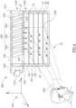
- Fig. 4 schematically shows a waveguide combiner 500 that expands an input aperture 535 in two, optionally orthogonal, directions to provide an expanded output coupling region 536 through which the waveguide combiner directs light into an EMB 560, in accordance with an embodiment of the disclosure.
- Waveguide combiner 500 optionally comprises a prismatic input coupler 550 a first waveguide 530 and a second waveguide 630, in accordance with an embodiment of the disclosure.
- Input coupler 550 receives light from virtual images generated by a laser display engine 570 through input aperture 535 and inputs the light into waveguide 530.
- Waveguide 530 comprises first and second TIR face surfaces 531 and 532 respectively that are parallel, arbitrarily, to the xy-plane of coordinate system 100, and top and bottom surfaces 532 and 534.
- the waveguide has an output coupler 540 comprising a plurality of parallel facets 542 in accordance with an embodiment of the disclosure.
- the facets are perpendicular to face surfaces 531 and 532 and are rotated about the z-axis by a tilt angle ⁇ *.
- the facets are evenly spaced.
- Light rays in light received from input coupler 550 are repeatedly totally reflected by and bounced back and forth between TIR face surfaces 531 and 532 until they reach and are incident on facets 542 of output coupler 540.
- Facets 542 are distributed over a relatively extended distance in the x-axis direction and reflect the light rays out of waveguide 530 in a general direction of the minus y-axis and into waveguide 630 through an extended output aperture 545 that expands input aperture 535 in the x-direction.
- Waveguide 630 may be any waveguide configured to receive light from an image generated by a display engine via an input aperture such as input aperture 535 and project the received light out from the waveguide via an output coupling region such as output coupling region 545 that is expanded substantially in a single direction.
- Waveguide 630 is assumed by way of example to be similar to waveguide 30, comprises facets 42 and TIR face surfaces 31 and 32 that are parallel to the xy-plane and are optionally continuous with face surfaces 531 and 532 respectively.
- Waveguide 630 expands the image in 545 of waveguide 530 in the minus y-direction and reflects the light it receives from waveguide 530 through an output coupling region 536 extended in both the x and y directions into EMB 560. It is noted that whereas waveguide 630 is assumed similar to waveguide 30 shown in Fig. 1A , waveguide 630 may be similar to any of various waveguides, for example waveguide 330 ( Fig. 2A ) or waveguide 430 ( Fig. 3A ) comprising facets and configured in accordance with an embodiment of the disclosure.
- Equations 25) and 26) may be chained to relate desired constraints on an output field of view that waveguide combiner 500 provides for EMB 560.
- One of the upward and down directed groups of light rays propagating in waveguide 530 is reflected by facets 542 into waveguide 630.
- v u (530) light rays are reflected into waveguide 630.
- a v u (530) light ray after reflection by a facet 542 enters waveguide 630 as an upward directed light ray relative to face surfaces 31 and 32.
- the upward directed light ray after entry into waveguide 630 be represented by v u (630).
- Upward and downward directed light rays in waveguide 630 are contained respectively in upward and downward directed fields of view wFOV-U and wFOV-D as schematically shown in Figs. 1A , 2A , and 3A .
- light rays in one of wFOV-U and wFOV-D in waveguide 630 are selected for reflection by facets 42 through output coupling region 536 in an output field of view O-FOV into EMB 560. Desired constraints on light rays in O-FOV may be back propagated to harmonize tilt angles ⁇ and ⁇ * that characterize facets 42 and 542 in waveguides 30 and 530.
- each of the verbs, "comprise” “include” and “have”, and conjugates thereof, are used to indicate that the object or objects of the verb are not necessarily a complete listing of components, elements or parts of the subject or subjects of the verb.
Landscapes
- Physics & Mathematics (AREA)
- General Physics & Mathematics (AREA)
- Optics & Photonics (AREA)
- Optical Integrated Circuits (AREA)
- Optical Couplings Of Light Guides (AREA)
Claims (11)
- Ein Wellenleiterkombinator (20), welcher Folgendes umfasst:einen ersten Wellenleiter (30), der eine erste (31) und eine zweite (32) parallele, vollständig reflektierende Innenfläche mit einer Normalen "nw" aufweist;eine Eingangsöffnung (35), durch die Licht in den ersten Wellenleiter (30) eintritt;eine Ausgangskopplungskonfiguration, die mit einem Ausgangskopplungsbereich (36) verbunden ist, der die Eingangsöffnung (35) in mindestens eine Richtung erweitert, und durch den Licht, das in den ersten Wellenleiter (30) eintritt, den ersten Wellenleiter (30) verlässt; undeinen Ausgangskoppler (40), der eine Vielzahl von parallelen Facetten (42) umfasst, die in den ersten Wellenleiter (30) eingebettet sind und einen Facettenneigungswinkel β zwischen nw und einer Normalen "nf" zu den Facetten aufweisen, wobei die Facetten (42) Licht reflektieren, das sich entlang des ersten Wellenleiters (30) ausbreitet und auf die Facetten (42) durch den Ausgangskopplungsbereich (36) hinaus einfällt, wobei die Facetten (42) Folgendes aufweisen:ein Facettenwellenlängenband für jedes Laserband von mindestens einem Laserband von Licht, das von einem Laser bereitgestellt wird, der Lichtwellenlängen in dem Laserband und in einem Wellenlängenbereich umfasst, über den das Laserband voraussichtlich variiert;einen Reflexionswinkelbereich, der ein erstes Reflexionsvermögen für Licht mit einer Wellenlänge im Facettenwellenlängenband aufweist, das sich in dem ersten Wellenleiter ausbreitet und in einem ersten Bereich von Einfallswinkeln auf die Facetten einfällt;einen Transmissionswinkelbereich, der ein zweites Reflexionsvermögen aufweist, das geringer ist als das erste Reflexionsvermögen für Licht mit einer Wellenlänge im Facettenwellenlängenband, das sich in dem ersten Wellenleiter ausbreitet und in einem zweiten Bereich von Einfallswinkeln auf die Facetten einfällt; undeinen durchsichtigen Winkeldurchlässigkeitsbereich mit hoher Durchlässigkeit für natürliches Licht, das in einem dritten Bereich von Einfallswinkeln auf die Facetten fällt;dadurch gekennzeichnet, dass:(90°- γ) > β, γ > θc, wobei gein Winkel zwischen nw und einer Einfallsrichtung auf die Stirnflächen eines Lichtstrahls, der sich in dem ersten Wellenleiter (30) ausbreitet und von dem der Ausgangskoppler (40) Licht durch den Ausgangskopplungsbereich (36) aus dem ersten Wellenleiter (30) heraus reflektiert, darstellt und θc einen kritischen Winkel des ersten Wellenleiters (30) für Licht mit einer Wellenlänge im Wellenlängenband der Facette (42) darstellt;wobei der Neigungswinkel β die Bedingung (θc+ α+)/2 < β < (30°+ α-/3), erfüllt, wobei α+ und α- Winkel in einer Ebene senkrecht zu den Stirnflächen (31, 32) und zu den Facetten (42) sind, die die Normale zu den Stirnflächen (31, 32) mit Richtungen bilden, entlang derer die Facetten (42) einfallendes Licht aus dem ersten Wellenleiter (30) heraus reflektieren, und wobei α+ größer als α- und positiv ist, wenn es im Uhrzeigersinn gedreht wird, und negativ, wenn es gegen den Uhrzeigersinn in Bezug auf die Normale gedreht wird, und wobei α+ und α- jeweils minimale und maximale Werte von γ bestimmen, die ein Sichtfeld, wFOV, von sich in dem ersten Wellenleiter (30) ausbreitendem Licht definieren;wobei der Reflexionswinkelbereich eine Skala von Einfallswinkeln überspannt, φ für die (β - α+) ≤ φ ≤ (β - α-);und wobei der Transmissionswinkelbereich eine Skala von Einfallswinkeln überspannt, φ für die (3β - α+) ≤ φ ≤ (3β - α-).
- Der Wellenleiterkombinator nach Anspruch 1, wobei für jedes Facettenwellenlängenband die Reflexionsvermögen für die Wellenlängen in dem Band um weniger als eine Obergrenze relativ zu einer durchschnittlichen Reflexionsvermögen in dem Wellenlängenband variiert, so dass ein Farbskala-Chromatizitätsdiskrepanzradius "ΔCG" in einem CIE 1931 xy-Chromatizitätsraum kleiner als oder gleich etwa 0,02 ist.
- Der Wellenleiterkombinator nach Anspruch 2, wobei, wenn ein durchschnittliches Reflexionsvermögen für Wellenlängen im Facettenwellenlängenband durch R dargestellt wird und eine maximale Differenz zwischen dem Reflexionsvermögen für eine Wellenlänge im Facettenwellenlängenband und R durch ΔR dargestellt wird, dann ist |ΔR|/R kleiner als oder gleich etwa 3%.
- Der Wellenleiterkombinator nach einem der vorhergehenden Ansprüche, wobei das mindestens eine Laserband mindestens eines oder eine beliebige Kombination von mehr als einem roten, grünen und/oder blauen Laserband umfasst.
- Der Wellenleiterkombinator nach einem der vorhergehenden Ansprüche, wobei das Facettenwellenlängenband für ein Laserband des mindestens einen Laserbandes eine Bandbreite aufweist, die größer oder gleich dem Dreifachen oder größer oder gleich dem Vierfachen der Bandbreite des Laserbandes ist.
- Der Wellenleiterkombinator nach einem der Ansprüche 1-5, wobei β > (90°- γ) .
- Der Wellenleiterkombinator nach Anspruch 6, wobei der Neigungswinkel β eine Einschränkung (30o+ α+/3) < β < (45° + α-/2) erfüllt.
- Der Wellenleiterkombinator nach Anspruch 7, wobei der Reflexionswinkelbereich eine Skala von Einfallswinkeln umfasst, φ für die (β - α+) ≤ φ ≤ (β - α-).
- Der Wellenleiterkombinator nach Anspruch 7 oder Anspruch 8, wobei der Transmissionswinkelbereich eine Reihe von Einfallswinkeln umfasst, φ für die,

- Der Wellenleiterkombinator nach Anspruch 6, wobei der Neigungswinkel β die Bedingung 45°- α-/2 < β < 90°-(α+ + θc)/2 erfüllt.
- Der Wellenleiterkombinator nach einem der vorhergehenden Ansprüche, der einen zweiten Wellenleiter (630) mit einer zweiten Eingangsöffnung und einem zweiten Ausgangskopplungsbereich umfasst, durch den Licht, das durch die zweite Eingangsöffnung empfangen wird, aus dem zweiten Wellenleiter (630) austritt und in den ersten Wellenleiter (30, 530) eintritt, und wobei der zweite Ausgangskopplungsbereich relativ zur zweiten Eingangsöffnung in einer Richtung erweitert ist, die sich von der mindestens einen Richtung unterscheidet, in der die Ausgangsöffnung des ersten Wellenleiters (30, 530) erweitert ist.
Applications Claiming Priority (3)
| Application Number | Priority Date | Filing Date | Title |
|---|---|---|---|
| US202062980469P | 2020-02-24 | 2020-02-24 | |
| US202063001567P | 2020-03-30 | 2020-03-30 | |
| PCT/IL2021/050206 WO2021171289A1 (en) | 2020-02-24 | 2021-02-22 | Mixed reality combiner |
Publications (3)
| Publication Number | Publication Date |
|---|---|
| EP4042233A1 EP4042233A1 (de) | 2022-08-17 |
| EP4042233A4 EP4042233A4 (de) | 2022-11-23 |
| EP4042233B1 true EP4042233B1 (de) | 2024-08-21 |
Family
ID=77490772
Family Applications (1)
| Application Number | Title | Priority Date | Filing Date |
|---|---|---|---|
| EP21761635.8A Active EP4042233B1 (de) | 2020-02-24 | 2021-02-22 | Mixed-reality-kombinierer |
Country Status (8)
| Country | Link |
|---|---|
| US (1) | US12455450B2 (de) |
| EP (1) | EP4042233B1 (de) |
| JP (2) | JP7709209B2 (de) |
| KR (1) | KR20220136367A (de) |
| CN (2) | CN115104059B (de) |
| IL (1) | IL294538B2 (de) |
| TW (1) | TWI889763B (de) |
| WO (1) | WO2021171289A1 (de) |
Cited By (1)
| Publication number | Priority date | Publication date | Assignee | Title |
|---|---|---|---|---|
| EP4270092B1 (de) * | 2020-12-28 | 2025-07-30 | FUJIFILM Corporation | Lichtleiter und videoanzeigevorrichtung |
Families Citing this family (5)
| Publication number | Priority date | Publication date | Assignee | Title |
|---|---|---|---|---|
| JP7728592B2 (ja) | 2020-04-30 | 2025-08-25 | ルムス エルティーディー. | 光学材料のサンプルの光学試験のための装置 |
| KR102638480B1 (ko) | 2020-11-09 | 2024-02-19 | 루머스 리미티드 | 역반사되는 환경의 주변광의 색도를 조절하는 방법 |
| JP7490286B2 (ja) | 2021-02-25 | 2024-05-27 | ルーマス リミテッド | 矩形導波路を有する光学アパーチャ増倍器 |
| IL313871A (en) | 2022-01-07 | 2024-08-01 | Lumus Ltd | Optical system for image orientation for viewing |
| CN114779479B (zh) * | 2022-06-21 | 2022-12-02 | 北京灵犀微光科技有限公司 | 近眼显示装置及穿戴设备 |
Family Cites Families (252)
| Publication number | Priority date | Publication date | Assignee | Title |
|---|---|---|---|---|
| US2748659A (en) | 1951-02-26 | 1956-06-05 | Jenaer Glaswerk Schott & Gen | Light source, searchlight or the like for polarized light |
| US2886911A (en) | 1953-07-23 | 1959-05-19 | George K C Hardesty | Duo-panel edge illumination system |
| US2795069A (en) | 1956-02-07 | 1957-06-11 | George K C Hardesty | Laminated metal-plastic illuminable panel |
| US3491245A (en) | 1967-04-10 | 1970-01-20 | George K C Hardesty | Guided light display panel |
| GB1330836A (en) | 1969-11-24 | 1973-09-19 | Vickers Ltd | Optical field-flattening devices |
| US3626394A (en) | 1970-04-09 | 1971-12-07 | Magnavox Co | Magneto-optical system |
| US3667621A (en) | 1970-10-20 | 1972-06-06 | Wisconsin Foundry And Machine | Fluid power system for a self-contained unloading unit |
| US3737212A (en) | 1970-12-14 | 1973-06-05 | Gen Electric | Diffraction optics head up display |
| GB1377627A (en) | 1971-09-01 | 1974-12-18 | Rank Organisation Ltd | Beam splitting prisms |
| US3857109A (en) | 1973-11-21 | 1974-12-24 | Us Navy | Longitudinally-pumped two-wavelength lasers |
| US3873209A (en) | 1973-12-10 | 1975-03-25 | Bell Telephone Labor Inc | Measurement of thin films by optical waveguiding technique |
| FR2295436A1 (fr) | 1974-12-16 | 1976-07-16 | Radiotechnique Compelec | Dispositif coupleur directif pour fibres optiques multimodes |
| US3940204A (en) | 1975-01-23 | 1976-02-24 | Hughes Aircraft Company | Optical display systems utilizing holographic lenses |
| US4084883A (en) | 1977-02-28 | 1978-04-18 | The University Of Rochester | Reflective polarization retarder and laser apparatus utilizing same |
| DE3000402A1 (de) | 1979-01-19 | 1980-07-31 | Smiths Industries Ltd | Anzeigevorrichtung |
| US4331387A (en) | 1980-07-03 | 1982-05-25 | Westinghouse Electric Corp. | Electro-optical modulator for randomly polarized light |
| GB2108702B (en) | 1981-10-14 | 1985-06-19 | Marconi Avionics | Optical arrangements |
| US4516828A (en) | 1982-05-03 | 1985-05-14 | General Motors Corporation | Duplex communication on a single optical fiber |
| FR2562273B1 (fr) | 1984-03-27 | 1986-08-08 | France Etat Armement | Dispositif d'observation a travers une paroi dans deux directions opposees |
| US4715684A (en) | 1984-06-20 | 1987-12-29 | Hughes Aircraft Company | Optical system for three color liquid crystal light valve image projection system |
| US4711512A (en) | 1985-07-12 | 1987-12-08 | Environmental Research Institute Of Michigan | Compact head-up display |
| US4720189A (en) | 1986-01-07 | 1988-01-19 | Northern Telecom Limited | Eye-position sensor |
| US4805988A (en) | 1987-07-24 | 1989-02-21 | Nelson Dones | Personal video viewing device |
| US4798448A (en) | 1988-02-16 | 1989-01-17 | General Electric Company | High efficiency illumination system for display devices |
| US4932743A (en) | 1988-04-18 | 1990-06-12 | Ricoh Company, Ltd. | Optical waveguide device |
| DE68909553T2 (de) | 1988-10-21 | 1994-01-27 | Thomson Csf | Optisches Kollimationssystem für eine Helmsichtanzeige. |
| CN1043203A (zh) | 1988-12-02 | 1990-06-20 | 三井石油化学工业株式会社 | 光输出控制方法及其装置 |
| US4978952A (en) | 1989-02-24 | 1990-12-18 | Collimated Displays Incorporated | Flat screen color video display |
| FR2647556B1 (fr) | 1989-05-23 | 1993-10-29 | Thomson Csf | Dispositif optique pour l'introduction d'une image collimatee dans le champ visuel d'un observateur et casque comportant au moins un tel dispositif |
| JPH04219657A (ja) | 1990-04-13 | 1992-08-10 | Ricoh Co Ltd | 光磁気情報記録再生装置及びモードスプリッタ |
| JPH04289531A (ja) | 1990-05-21 | 1992-10-14 | Ricoh Co Ltd | 光情報記録再生装置及びプリズム結合器 |
| US5157526A (en) | 1990-07-06 | 1992-10-20 | Hitachi, Ltd. | Unabsorbing type polarizer, method for manufacturing the same, polarized light source using the same, and apparatus for liquid crystal display using the same |
| US5096520A (en) | 1990-08-01 | 1992-03-17 | Faris Sades M | Method for producing high efficiency polarizing filters |
| US5751480A (en) | 1991-04-09 | 1998-05-12 | Canon Kabushiki Kaisha | Plate-like polarizing element, a polarizing conversion unit provided with the element, and a projector provided with the unit |
| FR2683918B1 (fr) | 1991-11-19 | 1994-09-09 | Thomson Csf | Materiau constitutif d'une lunette de visee et arme utilisant cette lunette. |
| US5270748A (en) | 1992-01-30 | 1993-12-14 | Mak Technologies, Inc. | High-speed eye tracking device and method |
| US5367399A (en) | 1992-02-13 | 1994-11-22 | Holotek Ltd. | Rotationally symmetric dual reflection optical beam scanner and system using same |
| US5301067A (en) | 1992-05-06 | 1994-04-05 | Plx Inc. | High accuracy periscope assembly |
| US5231642A (en) | 1992-05-08 | 1993-07-27 | Spectra Diode Laboratories, Inc. | Semiconductor ring and folded cavity lasers |
| US5369415A (en) | 1992-06-29 | 1994-11-29 | Motorola, Inc. | Direct retinal scan display with planar imager |
| CA2142332A1 (en) | 1992-08-13 | 1994-03-03 | Meinrad Machler | Spectroscopic systems for the analysis of small and very small quantities of substances |
| US6144347A (en) | 1992-10-09 | 2000-11-07 | Sony Corporation | Head-mounted image display apparatus |
| US5537173A (en) | 1992-10-23 | 1996-07-16 | Olympus Optical Co., Ltd. | Film winding detecting means for a camera including control means for controlling proper and accurate winding and rewinding of a film |
| WO1994019712A1 (en) | 1993-02-26 | 1994-09-01 | Yeda Research & Development Co., Ltd. | Holographic optical devices |
| US5555329A (en) | 1993-11-05 | 1996-09-10 | Alliesignal Inc. | Light directing optical structure |
| JPH07199236A (ja) | 1993-12-28 | 1995-08-04 | Fujitsu Ltd | 光スイッチ及び光分配器 |
| JPH08114765A (ja) | 1994-10-15 | 1996-05-07 | Fujitsu Ltd | 偏光分離・変換素子並びにこれを用いた偏光照明装置及び投射型表示装置 |
| US5650873A (en) | 1995-01-30 | 1997-07-22 | Lockheed Missiles & Space Company, Inc. | Micropolarization apparatus |
| US5999836A (en) | 1995-06-06 | 1999-12-07 | Nelson; Robert S. | Enhanced high resolution breast imaging device and method utilizing non-ionizing radiation of narrow spectral bandwidth |
| GB9521210D0 (en) | 1995-10-17 | 1996-08-28 | Barr & Stroud Ltd | Display system |
| US5829854A (en) | 1996-09-26 | 1998-11-03 | Raychem Corporation | Angled color dispersement and recombination prism |
| US6204974B1 (en) | 1996-10-08 | 2001-03-20 | The Microoptical Corporation | Compact image display system for eyeglasses or other head-borne frames |
| JPH10133055A (ja) | 1996-10-31 | 1998-05-22 | Sharp Corp | 光結合器及びその製造方法 |
| US5919601A (en) | 1996-11-12 | 1999-07-06 | Kodak Polychrome Graphics, Llc | Radiation-sensitive compositions and printing plates |
| US5724163A (en) | 1996-11-12 | 1998-03-03 | Yariv Ben-Yehuda | Optical system for alternative or simultaneous direction of light originating from two scenes to the eye of a viewer |
| JPH10160961A (ja) | 1996-12-03 | 1998-06-19 | Mitsubishi Gas Chem Co Inc | 光学素子 |
| US5883684A (en) | 1997-06-19 | 1999-03-16 | Three-Five Systems, Inc. | Diffusively reflecting shield optically, coupled to backlit lightguide, containing LED's completely surrounded by the shield |
| US5896232A (en) | 1997-08-07 | 1999-04-20 | International Business Machines Corporation | Highly efficient and compact frontlighting for polarization-based reflection light valves |
| US6091548A (en) | 1997-10-01 | 2000-07-18 | Raytheon Company | Optical system with two-stage aberration correction |
| US6154321A (en) | 1998-01-20 | 2000-11-28 | University Of Washington | Virtual retinal display with eye tracking |
| US6231992B1 (en) | 1998-09-04 | 2001-05-15 | Yazaki Corporation | Partial reflector |
| US20030063042A1 (en) | 1999-07-29 | 2003-04-03 | Asher A. Friesem | Electronic utility devices incorporating a compact virtual image display |
| EP1272889A2 (de) | 1999-10-14 | 2003-01-08 | Stratos Product Development LLC | System zur darstellung von virtuellen bildern |
| US6264328B1 (en) | 1999-10-21 | 2001-07-24 | University Of Rochester | Wavefront sensor with off-axis illumination |
| IL136248A (en) | 2000-05-21 | 2004-08-31 | Elop Electrooptics Ind Ltd | System and method for changing light transmission through a substrate |
| ES2348532T3 (es) | 2000-06-05 | 2010-12-09 | Lumus Ltd | Dilatador de haces opticos guiado por un sustrato. |
| IL136849A (en) | 2000-06-18 | 2004-09-27 | Beamus Ltd | Optical dynamic devices particularly for beam steering and optical communication |
| DE60036733T2 (de) | 2000-07-24 | 2008-07-17 | Mitsubishi Rayon Co., Ltd. | Oberflächenbeleuchtungseinrichtung |
| KR100388819B1 (ko) | 2000-07-31 | 2003-06-25 | 주식회사 대양이앤씨 | 헤드 마운트 디스플레이용 광학 시스템 |
| US6490104B1 (en) | 2000-09-15 | 2002-12-03 | Three-Five Systems, Inc. | Illumination system for a micro display |
| IL138895A (en) | 2000-10-05 | 2005-08-31 | Elop Electrooptics Ind Ltd | Optical switching devices |
| US6542307B2 (en) | 2000-10-20 | 2003-04-01 | Three-Five Systems, Inc. | Compact near-eye illumination system |
| US6626906B1 (en) | 2000-10-23 | 2003-09-30 | Sdgi Holdings, Inc. | Multi-planar adjustable connector |
| US6690513B2 (en) | 2001-07-03 | 2004-02-10 | Jds Uniphase Corporation | Rhomb interleaver |
| US6791760B2 (en) | 2001-07-24 | 2004-09-14 | Itt Manufacturing Enterprises, Inc. | Planar diffractive relay |
| US6927694B1 (en) | 2001-08-20 | 2005-08-09 | Research Foundation Of The University Of Central Florida | Algorithm for monitoring head/eye motion for driver alertness with one camera |
| EP1433160A1 (de) | 2001-09-07 | 2004-06-30 | The Microoptical Corporation | Leichtgewichtige kompakte neu anbringbare, an der vorderseite gehaltene elektronische anzeige |
| JP2003140081A (ja) | 2001-11-06 | 2003-05-14 | Nikon Corp | ホログラムコンバイナ光学系 |
| FR2834799B1 (fr) | 2002-01-11 | 2004-04-16 | Essilor Int | Lentille ophtalmique presentant un insert de projection |
| IL148804A (en) | 2002-03-21 | 2007-02-11 | Yaacov Amitai | Optical device |
| DE10216169A1 (de) | 2002-04-12 | 2003-10-30 | Zeiss Carl Jena Gmbh | Anordnung zur Polarisation von Licht |
| US20070165192A1 (en) | 2006-01-13 | 2007-07-19 | Silicon Optix Inc. | Reduced field angle projection display system |
| ITTO20020625A1 (it) | 2002-07-17 | 2004-01-19 | Fiat Ricerche | Guida di luce per dispositivi di visualizzazione di tipo "head-mounted" o "head-up" |
| EP1418459A1 (de) | 2002-11-08 | 2004-05-12 | 3M Innovative Properties Company | Optisches Element mit kuboktaedrischem Polyeder als Strahlteiler oder Lichtstreuer |
| US20050174641A1 (en) | 2002-11-26 | 2005-08-11 | Jds Uniphase Corporation | Polarization conversion light integrator |
| US7206133B2 (en) | 2003-05-22 | 2007-04-17 | Optical Research Associates | Light distribution apparatus and methods for illuminating optical systems |
| US7475992B2 (en) | 2003-06-10 | 2009-01-13 | Abu-Ageel Nayef M | Light recycler and color display system including same |
| US7298940B2 (en) | 2003-06-10 | 2007-11-20 | Abu-Ageel Nayef M | Illumination system and display system employing same |
| US7400447B2 (en) | 2003-09-03 | 2008-07-15 | Canon Kabushiki Kaisha | Stereoscopic image display device |
| IL157836A (en) | 2003-09-10 | 2009-08-03 | Yaakov Amitai | Optical devices particularly for remote viewing applications |
| IL157837A (en) | 2003-09-10 | 2012-12-31 | Yaakov Amitai | Substrate-guided optical device particularly for three-dimensional displays |
| IL157838A (en) | 2003-09-10 | 2013-05-30 | Yaakov Amitai | High-brightness optical device |
| KR20050037085A (ko) | 2003-10-17 | 2005-04-21 | 삼성전자주식회사 | 광터널, 균일광 조명장치 및 이를 채용한 프로젝터 |
| US7101063B2 (en) | 2004-02-05 | 2006-09-05 | Hewlett-Packard Development Company, L.P. | Systems and methods for integrating light |
| KR101049605B1 (ko) | 2004-04-01 | 2011-07-14 | 윌리엄 씨. 토치 | 눈 움직임을 모니터하는 바이오센서, 커뮤니케이터, 및컨트롤러 및 그들의 사용 방법 |
| WO2005111669A1 (ja) | 2004-05-17 | 2005-11-24 | Nikon Corporation | 光学素子、コンバイナ光学系、及び画像表示装置 |
| TWI282017B (en) | 2004-05-28 | 2007-06-01 | Epistar Corp | Planar light device |
| IL162573A (en) | 2004-06-17 | 2013-05-30 | Lumus Ltd | Optical component in a large key conductive substrate |
| IL163361A (en) | 2004-08-05 | 2011-06-30 | Lumus Ltd | Optical device for light coupling into a guiding substrate |
| US7778508B2 (en) | 2004-12-06 | 2010-08-17 | Nikon Corporation | Image display optical system, image display unit, illuminating optical system, and liquid crystal display unit |
| US20060126181A1 (en) | 2004-12-13 | 2006-06-15 | Nokia Corporation | Method and system for beam expansion in a display device |
| US7413328B2 (en) | 2004-12-30 | 2008-08-19 | Honeywell International Inc. | Remotely coupled hybrid HUD backlight |
| IL166799A (en) | 2005-02-10 | 2014-09-30 | Lumus Ltd | Aluminum shale surfaces for use in a conductive substrate |
| EP1846796A1 (de) | 2005-02-10 | 2007-10-24 | Lumus Ltd | Substratgeführte optische einrichtung insbesondere für visionserweiterte optische systeme |
| US10073264B2 (en) | 2007-08-03 | 2018-09-11 | Lumus Ltd. | Substrate-guide optical device |
| EP1849033B1 (de) | 2005-02-10 | 2019-06-19 | Lumus Ltd | Substratgeführte optische einrichtung mit einer dünnen transparenten schicht |
| WO2006087709A1 (en) | 2005-02-17 | 2006-08-24 | Lumus Ltd. | Personal navigation system |
| US7573640B2 (en) | 2005-04-04 | 2009-08-11 | Mirage Innovations Ltd. | Multi-plane optical apparatus |
| US8187481B1 (en) | 2005-05-05 | 2012-05-29 | Coho Holdings, Llc | Random texture anti-reflection optical surface treatment |
| US7405881B2 (en) | 2005-05-30 | 2008-07-29 | Konica Minolta Holdings, Inc. | Image display apparatus and head mount display |
| US20070002191A1 (en) | 2005-07-01 | 2007-01-04 | Seiko Epson Corporation | Projector |
| US20070155277A1 (en) | 2005-07-25 | 2007-07-05 | Avi Amitai | Mobile/portable and personal pre-recorded sound effects electronic amplifier device/gadget |
| EP1922579B1 (de) | 2005-09-07 | 2015-08-19 | BAE Systems PLC | Projektionsanzeige mit zwei plattenartigen coplanaren, gitter enthaltenden wellenleitern |
| US10261321B2 (en) | 2005-11-08 | 2019-04-16 | Lumus Ltd. | Polarizing optical system |
| IL171820A (en) | 2005-11-08 | 2014-04-30 | Lumus Ltd | A polarizing optical component for light coupling within a conductive substrate |
| US8360578B2 (en) | 2006-01-26 | 2013-01-29 | Nokia Corporation | Eye tracker device |
| IL173715A0 (en) | 2006-02-14 | 2007-03-08 | Lumus Ltd | Substrate-guided imaging lens |
| IL174170A (en) | 2006-03-08 | 2015-02-26 | Abraham Aharoni | Device and method for two-eyed tuning |
| IL177618A (en) | 2006-08-22 | 2015-02-26 | Lumus Ltd | Optical component in conductive substrate |
| EP2142953B1 (de) | 2007-04-22 | 2019-06-05 | Lumus Ltd | Collimierende optische anordnung und system |
| US8139944B2 (en) | 2007-05-08 | 2012-03-20 | The Boeing Company | Method and apparatus for clearing an optical channel |
| IL183637A (en) | 2007-06-04 | 2013-06-27 | Zvi Lapidot | Head display system |
| US7589901B2 (en) | 2007-07-10 | 2009-09-15 | Microvision, Inc. | Substrate-guided relays for use with scanned beam light sources |
| US8414304B2 (en) | 2008-08-19 | 2013-04-09 | Plextronics, Inc. | Organic light emitting diode lighting devices |
| US20110166946A1 (en) | 2008-09-11 | 2011-07-07 | Nestec S.A. | Method of promoting and selling coffee |
| US7949214B2 (en) | 2008-11-06 | 2011-05-24 | Microvision, Inc. | Substrate guided relay with pupil expanding input coupler |
| US8317352B2 (en) | 2008-12-11 | 2012-11-27 | Robert Saccomanno | Non-invasive injection of light into a transparent substrate, such as a window pane through its face |
| US7949252B1 (en) | 2008-12-11 | 2011-05-24 | Adobe Systems Incorporated | Plenoptic camera with large depth of field |
| WO2010067114A1 (en) | 2008-12-12 | 2010-06-17 | Bae Systems Plc | Improvements in or relating to waveguides |
| CN102356338B (zh) | 2009-04-08 | 2015-03-11 | 国际商业机器公司 | 具有埋设光反射特征的光波导及其制造方法 |
| US9256007B2 (en) | 2009-04-21 | 2016-02-09 | Svv Technology Innovations, Inc. | Light collection and illumination systems employing planar waveguide |
| US9335604B2 (en) | 2013-12-11 | 2016-05-10 | Milan Momcilo Popovich | Holographic waveguide display |
| US20100291489A1 (en) | 2009-05-15 | 2010-11-18 | Api Nanofabrication And Research Corp. | Exposure methods for forming patterned layers and apparatus for performing the same |
| CN102549492B (zh) | 2009-09-28 | 2014-12-24 | 日本电气株式会社 | 光源装置以及使用该光源装置的投射型显示装置 |
| US20120249797A1 (en) | 2010-02-28 | 2012-10-04 | Osterhout Group, Inc. | Head-worn adaptive display |
| US11275482B2 (en) | 2010-02-28 | 2022-03-15 | Microsoft Technology Licensing, Llc | Ar glasses with predictive control of external device based on event input |
| US9028123B2 (en) | 2010-04-16 | 2015-05-12 | Flex Lighting Ii, Llc | Display illumination device with a film-based lightguide having stacked incident surfaces |
| JP5499985B2 (ja) | 2010-08-09 | 2014-05-21 | ソニー株式会社 | 表示装置組立体 |
| US8649099B2 (en) | 2010-09-13 | 2014-02-11 | Vuzix Corporation | Prismatic multiple waveguide for near-eye display |
| US9632315B2 (en) | 2010-10-21 | 2017-04-25 | Lockheed Martin Corporation | Head-mounted display apparatus employing one or more fresnel lenses |
| US8743464B1 (en) | 2010-11-03 | 2014-06-03 | Google Inc. | Waveguide with embedded mirrors |
| US9292973B2 (en) | 2010-11-08 | 2016-03-22 | Microsoft Technology Licensing, Llc | Automatic variable virtual focus for augmented reality displays |
| US9304319B2 (en) | 2010-11-18 | 2016-04-05 | Microsoft Technology Licensing, Llc | Automatic focus improvement for augmented reality displays |
| JP5645631B2 (ja) | 2010-12-13 | 2014-12-24 | 三菱電機株式会社 | 波長モニタ、光モジュールおよび波長モニタ方法 |
| KR101993565B1 (ko) | 2010-12-22 | 2019-06-26 | 시리얼 테크놀로지즈 에스.에이. | 관찰자 트래킹을 위한 조합된 광변조 장치 |
| JP2012160813A (ja) | 2011-01-31 | 2012-08-23 | Sony Corp | 画像データ送信装置、画像データ送信方法、画像データ受信装置および画像データ受信方法 |
| JP5720290B2 (ja) | 2011-02-16 | 2015-05-20 | セイコーエプソン株式会社 | 虚像表示装置 |
| EP2693027A4 (de) | 2011-03-31 | 2014-10-08 | Toyota Motor Co Ltd | Steuerungsvorrichtung für einen verbrennungsmotor und damit ausgestattetes fahrzeug |
| JP2012252091A (ja) | 2011-06-01 | 2012-12-20 | Sony Corp | 表示装置 |
| US9595009B2 (en) | 2011-06-29 | 2017-03-14 | International Business Machines Corporation | Code reviewer selection in a distributed software development environment |
| US8472119B1 (en) | 2011-08-12 | 2013-06-25 | Google Inc. | Image waveguide having a bend |
| JP6127359B2 (ja) | 2011-09-15 | 2017-05-17 | セイコーエプソン株式会社 | 虚像表示装置及び虚像表示装置の製造方法 |
| US9297996B2 (en) | 2012-02-15 | 2016-03-29 | Microsoft Technology Licensing, Llc | Laser illumination scanning |
| US8665178B1 (en) * | 2012-03-01 | 2014-03-04 | Google, Inc. | Partially-reflective waveguide stack and heads-up display using same |
| US8848289B2 (en) | 2012-03-15 | 2014-09-30 | Google Inc. | Near-to-eye display with diffractive lens |
| US8736963B2 (en) | 2012-03-21 | 2014-05-27 | Microsoft Corporation | Two-dimensional exit-pupil expansion |
| EP2842003B1 (de) | 2012-04-25 | 2019-02-27 | Rockwell Collins, Inc. | Holographisches weitwinkeldisplay |
| US9456744B2 (en) | 2012-05-11 | 2016-10-04 | Digilens, Inc. | Apparatus for eye tracking |
| IL219907A (en) | 2012-05-21 | 2017-08-31 | Lumus Ltd | Integrated head display system with eye tracking |
| US20130321432A1 (en) | 2012-06-01 | 2013-12-05 | QUALCOMM MEMES Technologies, Inc. | Light guide with embedded fresnel reflectors |
| NZ702897A (en) | 2012-06-11 | 2017-03-31 | Magic Leap Inc | Multiple depth plane three-dimensional display using a wave guide reflector array projector |
| US9671566B2 (en) | 2012-06-11 | 2017-06-06 | Magic Leap, Inc. | Planar waveguide apparatus with diffraction element(s) and system employing same |
| US8909985B2 (en) | 2012-07-12 | 2014-12-09 | International Business Machines Corporation | Multiple hyperswap replication sessions |
| TWI522690B (zh) | 2012-07-26 | 2016-02-21 | 揚昇照明股份有限公司 | 複合式導光板與顯示裝置 |
| US8913324B2 (en) | 2012-08-07 | 2014-12-16 | Nokia Corporation | Display illumination light guide |
| WO2014074202A2 (en) | 2012-08-20 | 2014-05-15 | The Regents Of The University Of California | Monocentric lens designs and associated imaging systems having wide field of view and high resolution |
| US8947783B2 (en) | 2013-01-02 | 2015-02-03 | Google Inc. | Optical combiner for near-eye display |
| JP6065630B2 (ja) | 2013-02-13 | 2017-01-25 | セイコーエプソン株式会社 | 虚像表示装置 |
| DE102013106392B4 (de) | 2013-06-19 | 2017-06-08 | Fraunhofer-Gesellschaft zur Förderung der angewandten Forschung e.V. | Verfahren zur Herstellung einer Entspiegelungsschicht |
| US10222535B2 (en) | 2013-07-02 | 2019-03-05 | 3M Innovative Properties Company | Flat light guide |
| US20160020965A1 (en) | 2013-08-07 | 2016-01-21 | Hitachi, Ltd. | Method and apparatus for dynamic monitoring condition control |
| US20150081313A1 (en) | 2013-09-16 | 2015-03-19 | Sunedison Llc | Methods and systems for photovoltaic site installation, commissioining, and provisioning |
| JP6225657B2 (ja) | 2013-11-15 | 2017-11-08 | セイコーエプソン株式会社 | 光学素子および画像表示装置並びにこれらの製造方法 |
| US9915826B2 (en) | 2013-11-27 | 2018-03-13 | Magic Leap, Inc. | Virtual and augmented reality systems and methods having improved diffractive grating structures |
| CN113568175B (zh) | 2013-11-27 | 2023-06-27 | 奇跃公司 | 虚拟和增强现实系统与方法 |
| US20160187651A1 (en) | 2014-03-28 | 2016-06-30 | Osterhout Group, Inc. | Safety for a vehicle operator with an hmd |
| CN108572449B (zh) | 2014-03-31 | 2021-09-14 | 联想(北京)有限公司 | 显示装置和电子设备 |
| CN106104364B (zh) | 2014-04-02 | 2019-09-20 | 依视路国际公司 | 根据给定眼镜架计算光学系统的方法 |
| IL232197B (en) | 2014-04-23 | 2018-04-30 | Lumus Ltd | Compact head-up display system |
| US9857586B2 (en) | 2014-04-30 | 2018-01-02 | Sharp Kabushiki Kaisha | Reflective projection display device |
| JP6096713B2 (ja) | 2014-05-21 | 2017-03-15 | 株式会社東芝 | 表示装置 |
| CN106937531B (zh) | 2014-06-14 | 2020-11-06 | 奇跃公司 | 用于产生虚拟和增强现实的方法和系统 |
| US9285591B1 (en) | 2014-08-29 | 2016-03-15 | Google Inc. | Compact architecture for near-to-eye display system |
| EP3201686B9 (de) | 2014-09-29 | 2022-01-12 | Magic Leap, Inc. | Architekturen und verfahren zur ausgabe von licht mit verschiedenen wellenlängen aus wellenleitern |
| IL235642B (en) | 2014-11-11 | 2021-08-31 | Lumus Ltd | A compact head-up display system is protected by an element with a super-thin structure |
| IL236490B (en) | 2014-12-25 | 2021-10-31 | Lumus Ltd | Substrate-guided optical device |
| IL236491B (en) | 2014-12-25 | 2020-11-30 | Lumus Ltd | A method for manufacturing an optical component in a conductive substrate |
| JP6994940B2 (ja) | 2015-01-06 | 2022-01-14 | ビュージックス コーポレーション | 光結合を用いたヘッドマウント型画像装置 |
| WO2016120669A1 (fr) | 2015-01-30 | 2016-08-04 | Arcelormittal | Procédé de préparation d'une tôle revêtue comprenant l'application d'une solution aqueuse comprenant un aminoacide et utilisation associée pour améliorer la résistance à la corrosion |
| US20160234485A1 (en) | 2015-02-09 | 2016-08-11 | Steven John Robbins | Display System |
| IL237337B (en) | 2015-02-19 | 2020-03-31 | Amitai Yaakov | A compact head-up display system with a uniform image |
| CA3109499C (en) | 2015-04-22 | 2024-11-19 | Gentex Corporation | METHODS AND DEVICES FOR CORRECTING OPTICAL ABERRATION |
| US9910276B2 (en) | 2015-06-30 | 2018-03-06 | Microsoft Technology Licensing, Llc | Diffractive optical elements with graded edges |
| NZ742532A (en) | 2015-11-04 | 2019-05-31 | Magic Leap Inc | Light field display metrology |
| IL244181B (en) | 2016-02-18 | 2020-06-30 | Amitai Yaakov | Compact head-up display system |
| US10473933B2 (en) | 2016-02-19 | 2019-11-12 | Microsoft Technology Licensing, Llc | Waveguide pupil relay |
| TW201732373A (zh) | 2016-02-24 | 2017-09-16 | Omron Tateisi Electronics Co | 顯示裝置 |
| CN107167919B (zh) | 2016-03-07 | 2021-08-03 | 精工爱普生株式会社 | 导光装置以及虚像显示装置 |
| JP6677036B2 (ja) | 2016-03-23 | 2020-04-08 | セイコーエプソン株式会社 | 画像表示装置及び光学素子 |
| CN107290816B (zh) | 2016-03-30 | 2020-04-24 | 中强光电股份有限公司 | 光波导元件以及具有此光波导元件的头戴式显示装置 |
| US20170343810A1 (en) | 2016-05-24 | 2017-11-30 | Osterhout Group, Inc. | Pre-assembled solid optical assembly for head worn computers |
| US20170293140A1 (en) | 2016-04-12 | 2017-10-12 | Ostendo Technologies, Inc. | Split Exit Pupil Heads-Up Display Systems and Methods |
| EP3458898B1 (de) | 2016-05-18 | 2023-02-15 | Lumus Ltd. | Kopfmontierte bildgebungsvorrichtung |
| US20170353714A1 (en) | 2016-06-06 | 2017-12-07 | Navid Poulad | Self-calibrating display system |
| WO2018013307A1 (en) | 2016-06-21 | 2018-01-18 | Ntt Docomo, Inc. | An illuminator for a wearable display |
| KR101989364B1 (ko) | 2016-07-29 | 2019-06-14 | 공주대학교 산학협력단 | 대면적 염료감응형 태양전지 봉지용 유리 조성물 및 이를 포함하는 페이스트 |
| TWI614527B (zh) * | 2016-08-18 | 2018-02-11 | 盧姆斯有限公司 | 具有一致影像之小型頭戴式顯示系統 |
| TWI721208B (zh) * | 2016-08-22 | 2021-03-11 | 美商魔法飛躍股份有限公司 | 奈米光柵方法及設備 |
| KR102781635B1 (ko) * | 2016-10-09 | 2025-03-13 | 루머스 리미티드 | 직사각형 도파관을 사용하는 개구 배율기 |
| WO2018087756A1 (en) | 2016-11-08 | 2018-05-17 | Lumus Ltd | Light-guide device with optical cutoff edge and corresponding production methods |
| WO2018100582A1 (en) | 2016-12-02 | 2018-06-07 | Lumus Ltd. | Optical system with compact collimating image projector |
| EP3397137B1 (de) | 2016-12-31 | 2019-10-30 | Lumus Ltd. | Augenverfolger basierend auf retinaler abbildung über ein lichtleitendes optisches element |
| WO2018127913A1 (en) | 2017-01-04 | 2018-07-12 | Lumus Ltd. | Optical system for near-eye displays |
| CN108445573B (zh) | 2017-02-16 | 2023-06-30 | 中强光电股份有限公司 | 光波导元件以及显示装置 |
| EP3397998B1 (de) | 2017-02-22 | 2025-07-23 | Lumus Ltd. | Optische lichtleiteranordnung |
| CN115097625A (zh) | 2017-03-21 | 2022-09-23 | 奇跃公司 | 光学设备、头戴式显示器、成像系统和对对象成像的方法 |
| TWI751262B (zh) | 2017-03-22 | 2022-01-01 | 以色列商魯姆斯有限公司 | 交疊的反射面構造 |
| JP2018165744A (ja) | 2017-03-28 | 2018-10-25 | セイコーエプソン株式会社 | 導光装置および表示装置 |
| IL251645B (en) | 2017-04-06 | 2018-08-30 | Lumus Ltd | Waveguide and method of production |
| CN108693641A (zh) * | 2017-04-10 | 2018-10-23 | 北京微美云息软件有限公司 | 全息波导显示扩展结构 |
| CN110869839B (zh) | 2017-07-19 | 2022-07-08 | 鲁姆斯有限公司 | 通过光导光学元件的硅基液晶照明器 |
| CN111183393B (zh) * | 2017-09-29 | 2024-03-19 | 鲁姆斯有限公司 | 增强现实显示器 |
| IL255049B (en) * | 2017-10-16 | 2022-08-01 | Oorym Optics Ltd | A compact, high-efficiency head-up display system |
| TWI829656B (zh) | 2017-10-22 | 2024-01-21 | 以色列商魯姆斯有限公司 | 採用光具座的頭戴式增強現實設備 |
| CN111373296B (zh) | 2017-11-21 | 2023-02-28 | 鲁姆斯有限公司 | 用于近眼显示器的光学孔径扩展布置 |
| US10423336B2 (en) | 2017-11-28 | 2019-09-24 | International Business Machines Corporation | Fast locate using imitation reads on tape drives |
| KR20200096274A (ko) | 2017-12-03 | 2020-08-11 | 루머스 리미티드 | 광학 장치 정렬 방법 |
| US20190170327A1 (en) | 2017-12-03 | 2019-06-06 | Lumus Ltd. | Optical illuminator device |
| WO2019106636A1 (en) | 2017-12-03 | 2019-06-06 | Lumus Ltd. | Optical device testing method and apparatus |
| CN111557092B (zh) | 2017-12-10 | 2022-09-27 | 鲁姆斯有限公司 | 图像投影仪 |
| AU2019205611A1 (en) | 2018-01-02 | 2020-01-30 | Lumus Ltd. | Augmented reality displays with active alignment and corresponding methods |
| US10506220B2 (en) | 2018-01-02 | 2019-12-10 | Lumus Ltd. | Augmented reality displays with active alignment and corresponding methods |
| US10551544B2 (en) | 2018-01-21 | 2020-02-04 | Lumus Ltd. | Light-guide optical element with multiple-axis internal aperture expansion |
| US10942355B2 (en) | 2018-01-22 | 2021-03-09 | Facebook Technologies, Llc | Systems, devices, and methods for tiled multi-monochromatic displays |
| KR102837843B1 (ko) | 2018-04-08 | 2025-07-23 | 루머스 리미티드 | 광학 샘플 특성화 |
| EP4339656A3 (de) | 2018-05-14 | 2024-06-05 | Lumus Ltd. | Projektorkonfiguration mit unterteilter optischer apertur für augennahe anzeigen und entsprechende optische systeme |
| CN108681067A (zh) * | 2018-05-16 | 2018-10-19 | 上海鲲游光电科技有限公司 | 一种扩展视场角的波导显示装置 |
| CN112119344B (zh) | 2018-05-17 | 2023-01-20 | 鲁姆斯有限公司 | 具有交叠投射仪组件的近眼显示器 |
| IL259518B2 (en) | 2018-05-22 | 2023-04-01 | Lumus Ltd | Optical system and method for improving light field uniformity |
| BR112020023513A2 (pt) | 2018-05-23 | 2021-02-09 | Lumus Ltd. | sistema óptico |
| TWM587757U (zh) | 2018-05-27 | 2019-12-11 | 以色列商魯姆斯有限公司 | 具有場曲率影響減輕的基於基板引導的光學系統 |
| US11454590B2 (en) | 2018-06-21 | 2022-09-27 | Lumus Ltd. | Measurement technique for refractive index inhomogeneity between plates of a lightguide optical element (LOE) |
| US11415812B2 (en) | 2018-06-26 | 2022-08-16 | Lumus Ltd. | Compact collimating optical device and system |
| EP3824335B1 (de) | 2018-07-16 | 2023-10-18 | Lumus Ltd. | Optisches lichtleitelement mit polarisierten internen reflektoren |
| TWI871876B (zh) | 2018-08-26 | 2025-02-01 | 以色列商魯姆斯有限公司 | 近眼顯示器 |
| CN108983425A (zh) * | 2018-08-29 | 2018-12-11 | 深圳珑璟光电技术有限公司 | 一种二维出瞳扩展波导近眼光学显示装置 |
| TWI827663B (zh) | 2018-09-06 | 2024-01-01 | 以色列商魯姆斯有限公司 | 具有雷射二極體照明的近眼顯示器 |
| TWI865343B (zh) | 2018-09-09 | 2024-12-01 | 以色列商魯姆斯有限公司 | 包括具有二維擴展的光導光學元件的光學系統 |
| CN109239835A (zh) | 2018-10-19 | 2019-01-18 | 成都理想境界科技有限公司 | 波导、成像扩展模组、光源模组、近眼显示系统及设备 |
| JP3226277U (ja) | 2018-11-11 | 2020-05-14 | ルムス エルティーディー. | 中間ウィンドウを有するニアアイディスプレイ |
| EP4220276B1 (de) | 2019-01-24 | 2025-10-15 | Lumus Ltd. | Optische systeme mit loe mit dreistufiger expansion |
| KR20250142979A (ko) | 2019-05-06 | 2025-09-30 | 루머스 리미티드 | 장면 및 근안 디스플레이를 관찰시키기 위한 투명 광 가이드 |
-
2021
- 2021-02-22 EP EP21761635.8A patent/EP4042233B1/de active Active
- 2021-02-22 JP JP2022543019A patent/JP7709209B2/ja active Active
- 2021-02-22 US US17/776,126 patent/US12455450B2/en active Active
- 2021-02-22 CN CN202180013816.6A patent/CN115104059B/zh active Active
- 2021-02-22 WO PCT/IL2021/050206 patent/WO2021171289A1/en not_active Ceased
- 2021-02-22 CN CN202511025409.3A patent/CN120703984A/zh active Pending
- 2021-02-22 KR KR1020227027843A patent/KR20220136367A/ko active Pending
- 2021-02-24 TW TW110106564A patent/TWI889763B/zh active
-
2022
- 2022-07-05 IL IL294538A patent/IL294538B2/en unknown
-
2025
- 2025-06-27 JP JP2025109549A patent/JP2025133786A/ja active Pending
Cited By (1)
| Publication number | Priority date | Publication date | Assignee | Title |
|---|---|---|---|---|
| EP4270092B1 (de) * | 2020-12-28 | 2025-07-30 | FUJIFILM Corporation | Lichtleiter und videoanzeigevorrichtung |
Also Published As
| Publication number | Publication date |
|---|---|
| EP4042233A1 (de) | 2022-08-17 |
| US12455450B2 (en) | 2025-10-28 |
| IL294538B2 (en) | 2025-12-01 |
| CN115104059A (zh) | 2022-09-23 |
| KR20220136367A (ko) | 2022-10-07 |
| JP2025133786A (ja) | 2025-09-11 |
| EP4042233A4 (de) | 2022-11-23 |
| TWI889763B (zh) | 2025-07-11 |
| WO2021171289A1 (en) | 2021-09-02 |
| TW202138852A (zh) | 2021-10-16 |
| IL294538A (en) | 2022-09-01 |
| JP2023514807A (ja) | 2023-04-11 |
| JP7709209B2 (ja) | 2025-07-16 |
| CN115104059B (zh) | 2025-08-19 |
| CN120703984A (zh) | 2025-09-26 |
| WO2021171289A8 (en) | 2022-11-17 |
| US20220397766A1 (en) | 2022-12-15 |
| IL294538B1 (en) | 2025-08-01 |
Similar Documents
| Publication | Publication Date | Title |
|---|---|---|
| EP4042233B1 (de) | Mixed-reality-kombinierer | |
| US11536975B2 (en) | Overlapping facets | |
| AU2023203502B2 (en) | Optical systems including loe with three stage expansion | |
| US10048499B2 (en) | Polarizing optical system | |
| US7643214B2 (en) | Substrate-guided optical device with wide aperture | |
| US20090128911A1 (en) | Diffraction Grating With a Spatially Varying Duty-Cycle | |
| US12487457B2 (en) | Virtual image delivery system for near eye displays | |
| JP2017003845A (ja) | 導光装置及び虚像表示装置 | |
| KR20230144000A (ko) | 리타더 요소가 있는 2차원 확장을 위한 광 가이드 광학 요소를 포함하는 광학 시스템 |
Legal Events
| Date | Code | Title | Description |
|---|---|---|---|
| STAA | Information on the status of an ep patent application or granted ep patent |
Free format text: STATUS: THE INTERNATIONAL PUBLICATION HAS BEEN MADE |
|
| PUAI | Public reference made under article 153(3) epc to a published international application that has entered the european phase |
Free format text: ORIGINAL CODE: 0009012 |
|
| STAA | Information on the status of an ep patent application or granted ep patent |
Free format text: STATUS: REQUEST FOR EXAMINATION WAS MADE |
|
| 17P | Request for examination filed |
Effective date: 20220324 |
|
| AK | Designated contracting states |
Kind code of ref document: A1 Designated state(s): AL AT BE BG CH CY CZ DE DK EE ES FI FR GB GR HR HU IE IS IT LI LT LU LV MC MK MT NL NO PL PT RO RS SE SI SK SM TR |
|
| A4 | Supplementary search report drawn up and despatched |
Effective date: 20221025 |
|
| RIC1 | Information provided on ipc code assigned before grant |
Ipc: G02B 27/01 20060101AFI20221019BHEP |
|
| DAV | Request for validation of the european patent (deleted) | ||
| DAX | Request for extension of the european patent (deleted) | ||
| P01 | Opt-out of the competence of the unified patent court (upc) registered |
Effective date: 20230527 |
|
| GRAP | Despatch of communication of intention to grant a patent |
Free format text: ORIGINAL CODE: EPIDOSNIGR1 |
|
| STAA | Information on the status of an ep patent application or granted ep patent |
Free format text: STATUS: GRANT OF PATENT IS INTENDED |
|
| INTG | Intention to grant announced |
Effective date: 20240408 |
|
| GRAS | Grant fee paid |
Free format text: ORIGINAL CODE: EPIDOSNIGR3 |
|
| GRAA | (expected) grant |
Free format text: ORIGINAL CODE: 0009210 |
|
| STAA | Information on the status of an ep patent application or granted ep patent |
Free format text: STATUS: THE PATENT HAS BEEN GRANTED |
|
| AK | Designated contracting states |
Kind code of ref document: B1 Designated state(s): AL AT BE BG CH CY CZ DE DK EE ES FI FR GB GR HR HU IE IS IT LI LT LU LV MC MK MT NL NO PL PT RO RS SE SI SK SM TR |
|
| REG | Reference to a national code |
Ref country code: GB Ref legal event code: FG4D |
|
| REG | Reference to a national code |
Ref country code: CH Ref legal event code: EP |
|
| REG | Reference to a national code |
Ref country code: DE Ref legal event code: R096 Ref document number: 602021017609 Country of ref document: DE |
|
| REG | Reference to a national code |
Ref country code: IE Ref legal event code: FG4D |
|
| REG | Reference to a national code |
Ref country code: LT Ref legal event code: MG9D |
|
| REG | Reference to a national code |
Ref country code: NL Ref legal event code: MP Effective date: 20240821 |
|
| PG25 | Lapsed in a contracting state [announced via postgrant information from national office to epo] |
Ref country code: NO Free format text: LAPSE BECAUSE OF FAILURE TO SUBMIT A TRANSLATION OF THE DESCRIPTION OR TO PAY THE FEE WITHIN THE PRESCRIBED TIME-LIMIT Effective date: 20241121 |
|
| REG | Reference to a national code |
Ref country code: AT Ref legal event code: MK05 Ref document number: 1716070 Country of ref document: AT Kind code of ref document: T Effective date: 20240821 |
|
| PG25 | Lapsed in a contracting state [announced via postgrant information from national office to epo] |
Ref country code: NL Free format text: LAPSE BECAUSE OF FAILURE TO SUBMIT A TRANSLATION OF THE DESCRIPTION OR TO PAY THE FEE WITHIN THE PRESCRIBED TIME-LIMIT Effective date: 20240821 Ref country code: FI Free format text: LAPSE BECAUSE OF FAILURE TO SUBMIT A TRANSLATION OF THE DESCRIPTION OR TO PAY THE FEE WITHIN THE PRESCRIBED TIME-LIMIT Effective date: 20240821 Ref country code: PT Free format text: LAPSE BECAUSE OF FAILURE TO SUBMIT A TRANSLATION OF THE DESCRIPTION OR TO PAY THE FEE WITHIN THE PRESCRIBED TIME-LIMIT Effective date: 20241223 Ref country code: PL Free format text: LAPSE BECAUSE OF FAILURE TO SUBMIT A TRANSLATION OF THE DESCRIPTION OR TO PAY THE FEE WITHIN THE PRESCRIBED TIME-LIMIT Effective date: 20240821 Ref country code: GR Free format text: LAPSE BECAUSE OF FAILURE TO SUBMIT A TRANSLATION OF THE DESCRIPTION OR TO PAY THE FEE WITHIN THE PRESCRIBED TIME-LIMIT Effective date: 20241122 |
|
| PG25 | Lapsed in a contracting state [announced via postgrant information from national office to epo] |
Ref country code: BG Free format text: LAPSE BECAUSE OF FAILURE TO SUBMIT A TRANSLATION OF THE DESCRIPTION OR TO PAY THE FEE WITHIN THE PRESCRIBED TIME-LIMIT Effective date: 20240821 |
|
| PG25 | Lapsed in a contracting state [announced via postgrant information from national office to epo] |
Ref country code: LV Free format text: LAPSE BECAUSE OF FAILURE TO SUBMIT A TRANSLATION OF THE DESCRIPTION OR TO PAY THE FEE WITHIN THE PRESCRIBED TIME-LIMIT Effective date: 20240821 |
|
| PG25 | Lapsed in a contracting state [announced via postgrant information from national office to epo] |
Ref country code: AT Free format text: LAPSE BECAUSE OF FAILURE TO SUBMIT A TRANSLATION OF THE DESCRIPTION OR TO PAY THE FEE WITHIN THE PRESCRIBED TIME-LIMIT Effective date: 20240821 Ref country code: IS Free format text: LAPSE BECAUSE OF FAILURE TO SUBMIT A TRANSLATION OF THE DESCRIPTION OR TO PAY THE FEE WITHIN THE PRESCRIBED TIME-LIMIT Effective date: 20241221 |
|
| PG25 | Lapsed in a contracting state [announced via postgrant information from national office to epo] |
Ref country code: HR Free format text: LAPSE BECAUSE OF FAILURE TO SUBMIT A TRANSLATION OF THE DESCRIPTION OR TO PAY THE FEE WITHIN THE PRESCRIBED TIME-LIMIT Effective date: 20240821 |
|
| PG25 | Lapsed in a contracting state [announced via postgrant information from national office to epo] |
Ref country code: RS Free format text: LAPSE BECAUSE OF FAILURE TO SUBMIT A TRANSLATION OF THE DESCRIPTION OR TO PAY THE FEE WITHIN THE PRESCRIBED TIME-LIMIT Effective date: 20241121 Ref country code: ES Free format text: LAPSE BECAUSE OF FAILURE TO SUBMIT A TRANSLATION OF THE DESCRIPTION OR TO PAY THE FEE WITHIN THE PRESCRIBED TIME-LIMIT Effective date: 20240821 |
|
| PG25 | Lapsed in a contracting state [announced via postgrant information from national office to epo] |
Ref country code: RS Free format text: LAPSE BECAUSE OF FAILURE TO SUBMIT A TRANSLATION OF THE DESCRIPTION OR TO PAY THE FEE WITHIN THE PRESCRIBED TIME-LIMIT Effective date: 20241121 Ref country code: PT Free format text: LAPSE BECAUSE OF FAILURE TO SUBMIT A TRANSLATION OF THE DESCRIPTION OR TO PAY THE FEE WITHIN THE PRESCRIBED TIME-LIMIT Effective date: 20241223 Ref country code: PL Free format text: LAPSE BECAUSE OF FAILURE TO SUBMIT A TRANSLATION OF THE DESCRIPTION OR TO PAY THE FEE WITHIN THE PRESCRIBED TIME-LIMIT Effective date: 20240821 Ref country code: NO Free format text: LAPSE BECAUSE OF FAILURE TO SUBMIT A TRANSLATION OF THE DESCRIPTION OR TO PAY THE FEE WITHIN THE PRESCRIBED TIME-LIMIT Effective date: 20241121 Ref country code: NL Free format text: LAPSE BECAUSE OF FAILURE TO SUBMIT A TRANSLATION OF THE DESCRIPTION OR TO PAY THE FEE WITHIN THE PRESCRIBED TIME-LIMIT Effective date: 20240821 Ref country code: LV Free format text: LAPSE BECAUSE OF FAILURE TO SUBMIT A TRANSLATION OF THE DESCRIPTION OR TO PAY THE FEE WITHIN THE PRESCRIBED TIME-LIMIT Effective date: 20240821 Ref country code: IS Free format text: LAPSE BECAUSE OF FAILURE TO SUBMIT A TRANSLATION OF THE DESCRIPTION OR TO PAY THE FEE WITHIN THE PRESCRIBED TIME-LIMIT Effective date: 20241221 Ref country code: HR Free format text: LAPSE BECAUSE OF FAILURE TO SUBMIT A TRANSLATION OF THE DESCRIPTION OR TO PAY THE FEE WITHIN THE PRESCRIBED TIME-LIMIT Effective date: 20240821 Ref country code: GR Free format text: LAPSE BECAUSE OF FAILURE TO SUBMIT A TRANSLATION OF THE DESCRIPTION OR TO PAY THE FEE WITHIN THE PRESCRIBED TIME-LIMIT Effective date: 20241122 Ref country code: FI Free format text: LAPSE BECAUSE OF FAILURE TO SUBMIT A TRANSLATION OF THE DESCRIPTION OR TO PAY THE FEE WITHIN THE PRESCRIBED TIME-LIMIT Effective date: 20240821 Ref country code: ES Free format text: LAPSE BECAUSE OF FAILURE TO SUBMIT A TRANSLATION OF THE DESCRIPTION OR TO PAY THE FEE WITHIN THE PRESCRIBED TIME-LIMIT Effective date: 20240821 Ref country code: BG Free format text: LAPSE BECAUSE OF FAILURE TO SUBMIT A TRANSLATION OF THE DESCRIPTION OR TO PAY THE FEE WITHIN THE PRESCRIBED TIME-LIMIT Effective date: 20240821 Ref country code: AT Free format text: LAPSE BECAUSE OF FAILURE TO SUBMIT A TRANSLATION OF THE DESCRIPTION OR TO PAY THE FEE WITHIN THE PRESCRIBED TIME-LIMIT Effective date: 20240821 |
|
| PGFP | Annual fee paid to national office [announced via postgrant information from national office to epo] |
Ref country code: DE Payment date: 20250226 Year of fee payment: 5 |
|
| PG25 | Lapsed in a contracting state [announced via postgrant information from national office to epo] |
Ref country code: RO Free format text: LAPSE BECAUSE OF FAILURE TO SUBMIT A TRANSLATION OF THE DESCRIPTION OR TO PAY THE FEE WITHIN THE PRESCRIBED TIME-LIMIT Effective date: 20240821 Ref country code: DK Free format text: LAPSE BECAUSE OF FAILURE TO SUBMIT A TRANSLATION OF THE DESCRIPTION OR TO PAY THE FEE WITHIN THE PRESCRIBED TIME-LIMIT Effective date: 20240821 Ref country code: SM Free format text: LAPSE BECAUSE OF FAILURE TO SUBMIT A TRANSLATION OF THE DESCRIPTION OR TO PAY THE FEE WITHIN THE PRESCRIBED TIME-LIMIT Effective date: 20240821 |
|
| PG25 | Lapsed in a contracting state [announced via postgrant information from national office to epo] |
Ref country code: EE Free format text: LAPSE BECAUSE OF FAILURE TO SUBMIT A TRANSLATION OF THE DESCRIPTION OR TO PAY THE FEE WITHIN THE PRESCRIBED TIME-LIMIT Effective date: 20240821 |
|
| PG25 | Lapsed in a contracting state [announced via postgrant information from national office to epo] |
Ref country code: CZ Free format text: LAPSE BECAUSE OF FAILURE TO SUBMIT A TRANSLATION OF THE DESCRIPTION OR TO PAY THE FEE WITHIN THE PRESCRIBED TIME-LIMIT Effective date: 20240821 |
|
| PGFP | Annual fee paid to national office [announced via postgrant information from national office to epo] |
Ref country code: FR Payment date: 20250224 Year of fee payment: 5 |
|
| PG25 | Lapsed in a contracting state [announced via postgrant information from national office to epo] |
Ref country code: IT Free format text: LAPSE BECAUSE OF FAILURE TO SUBMIT A TRANSLATION OF THE DESCRIPTION OR TO PAY THE FEE WITHIN THE PRESCRIBED TIME-LIMIT Effective date: 20240821 Ref country code: SK Free format text: LAPSE BECAUSE OF FAILURE TO SUBMIT A TRANSLATION OF THE DESCRIPTION OR TO PAY THE FEE WITHIN THE PRESCRIBED TIME-LIMIT Effective date: 20240821 |
|
| PGFP | Annual fee paid to national office [announced via postgrant information from national office to epo] |
Ref country code: GB Payment date: 20250218 Year of fee payment: 5 |
|
| REG | Reference to a national code |
Ref country code: DE Ref legal event code: R097 Ref document number: 602021017609 Country of ref document: DE |
|
| PLBE | No opposition filed within time limit |
Free format text: ORIGINAL CODE: 0009261 |
|
| STAA | Information on the status of an ep patent application or granted ep patent |
Free format text: STATUS: NO OPPOSITION FILED WITHIN TIME LIMIT |
|
| 26N | No opposition filed |
Effective date: 20250522 |
|
| PG25 | Lapsed in a contracting state [announced via postgrant information from national office to epo] |
Ref country code: SE Free format text: LAPSE BECAUSE OF FAILURE TO SUBMIT A TRANSLATION OF THE DESCRIPTION OR TO PAY THE FEE WITHIN THE PRESCRIBED TIME-LIMIT Effective date: 20240821 |
|
| PG25 | Lapsed in a contracting state [announced via postgrant information from national office to epo] |
Ref country code: MC Free format text: LAPSE BECAUSE OF FAILURE TO SUBMIT A TRANSLATION OF THE DESCRIPTION OR TO PAY THE FEE WITHIN THE PRESCRIBED TIME-LIMIT Effective date: 20240821 |
|
| REG | Reference to a national code |
Ref country code: CH Ref legal event code: PL |
|
| PG25 | Lapsed in a contracting state [announced via postgrant information from national office to epo] |
Ref country code: LU Free format text: LAPSE BECAUSE OF NON-PAYMENT OF DUE FEES Effective date: 20250222 |
|
| PG25 | Lapsed in a contracting state [announced via postgrant information from national office to epo] |
Ref country code: CH Free format text: LAPSE BECAUSE OF NON-PAYMENT OF DUE FEES Effective date: 20250228 |