EP4037446B1 - Tastaturüberlagerung mit ableitung elektrostatischer entladung - Google Patents
Tastaturüberlagerung mit ableitung elektrostatischer entladung Download PDFInfo
- Publication number
- EP4037446B1 EP4037446B1 EP22154094.1A EP22154094A EP4037446B1 EP 4037446 B1 EP4037446 B1 EP 4037446B1 EP 22154094 A EP22154094 A EP 22154094A EP 4037446 B1 EP4037446 B1 EP 4037446B1
- Authority
- EP
- European Patent Office
- Prior art keywords
- conductive
- assembly
- overlay
- layer
- keypad
- Prior art date
- Legal status (The legal status is an assumption and is not a legal conclusion. Google has not performed a legal analysis and makes no representation as to the accuracy of the status listed.)
- Active
Links
Images



Classifications
-
- G—PHYSICS
- G06—COMPUTING OR CALCULATING; COUNTING
- G06F—ELECTRIC DIGITAL DATA PROCESSING
- G06F3/00—Input arrangements for transferring data to be processed into a form capable of being handled by the computer; Output arrangements for transferring data from processing unit to output unit, e.g. interface arrangements
- G06F3/01—Input arrangements or combined input and output arrangements for interaction between user and computer
- G06F3/02—Input arrangements using manually operated switches, e.g. using keyboards or dials
- G06F3/0202—Constructional details or processes of manufacture of the input device
-
- H—ELECTRICITY
- H05—ELECTRIC TECHNIQUES NOT OTHERWISE PROVIDED FOR
- H05K—PRINTED CIRCUITS; CASINGS OR CONSTRUCTIONAL DETAILS OF ELECTRIC APPARATUS; MANUFACTURE OF ASSEMBLAGES OF ELECTRICAL COMPONENTS
- H05K9/00—Screening of apparatus or components against electric or magnetic fields
- H05K9/0067—Devices for protecting against damage from electrostatic discharge
-
- H—ELECTRICITY
- H05—ELECTRIC TECHNIQUES NOT OTHERWISE PROVIDED FOR
- H05F—STATIC ELECTRICITY; NATURALLY-OCCURRING ELECTRICITY
- H05F3/00—Carrying-off electrostatic charges
- H05F3/04—Carrying-off electrostatic charges by means of spark gaps or other discharge devices
-
- H—ELECTRICITY
- H01—ELECTRIC ELEMENTS
- H01H—ELECTRIC SWITCHES; RELAYS; SELECTORS; EMERGENCY PROTECTIVE DEVICES
- H01H13/00—Switches having rectilinearly-movable operating part or parts adapted for pushing or pulling in one direction only, e.g. push-button switch
- H01H13/70—Switches having rectilinearly-movable operating part or parts adapted for pushing or pulling in one direction only, e.g. push-button switch having a plurality of operating members associated with different sets of contacts, e.g. keyboard
-
- H—ELECTRICITY
- H01—ELECTRIC ELEMENTS
- H01H—ELECTRIC SWITCHES; RELAYS; SELECTORS; EMERGENCY PROTECTIVE DEVICES
- H01H9/00—Details of switching devices, not covered by groups H01H1/00 - H01H7/00
- H01H9/48—Means for preventing discharge to non-current-carrying parts, e.g. using corona ring
-
- H—ELECTRICITY
- H05—ELECTRIC TECHNIQUES NOT OTHERWISE PROVIDED FOR
- H05K—PRINTED CIRCUITS; CASINGS OR CONSTRUCTIONAL DETAILS OF ELECTRIC APPARATUS; MANUFACTURE OF ASSEMBLAGES OF ELECTRICAL COMPONENTS
- H05K5/00—Casings, cabinets or drawers for electric apparatus
- H05K5/0017—Casings, cabinets or drawers for electric apparatus with operator interface units
-
- C—CHEMISTRY; METALLURGY
- C09—DYES; PAINTS; POLISHES; NATURAL RESINS; ADHESIVES; COMPOSITIONS NOT OTHERWISE PROVIDED FOR; APPLICATIONS OF MATERIALS NOT OTHERWISE PROVIDED FOR
- C09D—COATING COMPOSITIONS, e.g. PAINTS, VARNISHES OR LACQUERS; FILLING PASTES; CHEMICAL PAINT OR INK REMOVERS; INKS; CORRECTING FLUIDS; WOODSTAINS; PASTES OR SOLIDS FOR COLOURING OR PRINTING; USE OF MATERIALS THEREFOR
- C09D165/00—Coating compositions based on macromolecular compounds obtained by reactions forming a carbon-to-carbon link in the main chain; Coating compositions based on derivatives of such polymers
-
- C—CHEMISTRY; METALLURGY
- C09—DYES; PAINTS; POLISHES; NATURAL RESINS; ADHESIVES; COMPOSITIONS NOT OTHERWISE PROVIDED FOR; APPLICATIONS OF MATERIALS NOT OTHERWISE PROVIDED FOR
- C09D—COATING COMPOSITIONS, e.g. PAINTS, VARNISHES OR LACQUERS; FILLING PASTES; CHEMICAL PAINT OR INK REMOVERS; INKS; CORRECTING FLUIDS; WOODSTAINS; PASTES OR SOLIDS FOR COLOURING OR PRINTING; USE OF MATERIALS THEREFOR
- C09D5/00—Coating compositions, e.g. paints, varnishes or lacquers, characterised by their physical nature or the effects produced; Filling pastes
- C09D5/24—Electrically-conducting paints
Definitions
- the inventive concept relates to an overlay for a keypad for an electronic device, in which the overlay is adapted to dissipate electrostatic charges that may arise through use. While useful in any surroundings, the overlay incorporating the inventive concept provides the electronic device with a keypad that can meet or exceed standardized tests for use in an environment in which the sudden flow of electrons across a gap could ignite a flammable mixture, resulting in fire or an explosive flame front.
- plastic insulating materials are often used to construct a keyboard/display overlay, which is attached to the outside of a metal equipment enclosure. Due to its chemical properties, the plastic overlay can collect and hold a high energy static charge and then discharge suddenly, creating a potentially dangerous ignition spark, unless protective measures are employed to drain or dissipate the static charges as they arise.
- ITO indium-tin oxide
- electrostatic charge grounding is achieved by connecting an outer surface touchscreen conductive coating to a grounded conductor in a graphics terminal using an electrostatic charge routing system that provides a path for electrons that accumulate on the conductive coating to pass through one or more non-conductive elements in the graphics terminal.
- the grounded conductor can be a bezel made of metal or another conductor, a conductive paint layer applied to a bezel or other graphics terminal element, a metal spline pin or a metal screw.
- the electron path defined by the electrostatic charge routing system can include conductive and dissipative elements such as metal spline pins, metal screws, conductive epoxy, conducting plastic elements providing a short, closed electron bridge.
- an assembly for protecting, from electrostatic discharge, a plastic keypad having data entry elements and at least one display element comprises an overlay substrate and an electrically-conductive arrangement.
- the overlay substrate has a top side and a back side. It also has a plurality of precisely-positioned vias formed therethrough.
- the top side has a top surface coated with a layer of a conductive polymer and the back side has a back surface printed with at least one layer of color ink, the at least one layer of color ink depicting a plurality of alpha-numerical and pictorial elements of the keypad.
- the electrically-conductive arrangement is disposed on the overlay substrate to collect electrostatic charges on the top side, transfer the electrostatic charges to the back side through the plurality of vias and drain the transferred electrostatic charges to a ground.
- the electrically-conductive arrangement also comprises at least one first conductive grid printed onto the top surface of the overlay substrate beneath the layer of conductive polymer.
- This at least one first conductive grid divides the top surface into a plurality of surrounded areas, each of which is equal to or smaller than a predetermined size.
- Each of the first conductive grids comprises a plurality of nodes, wherein each node is positioned atop, and extending into, a corresponding one of the plurality of precisely-placed vias.
- the electrically-conductive arrangement also comprises at least one second conductive grid printed onto the back surface of the overlay substrate, below the at least one layer of color ink.
- Each second conductive grid corresponds in size and shape to one of the first conductive grids, and each of the second conductive grids comprises a plurality of nodes, with each node positioned below, and extending into, a corresponding one of the plurality of precisely-placed vias.
- the electrically-conductive arrangement also has at least one conductive connection that communicates to ground each second conductive grid.
- each of the first conductive grids and the second conductive grids comprises lengths of a conductive paste printed on the overlay substrate. In that situation, a layer of color ink is applied atop the lengths of conductive paste in each of the first conductive grids.
- the nodes of each of the first conductive grids comprise a plug of a conductive polymer applied to each of the precisely-positioned vias from the top side of the overlay substrate, a length of the conductive paste applied atop the plug; and a length of the color ink applied atop the length of conductive paste.
- the plug has a body portion that extends into the via and a flange portion, having a diameter that is larger than a diameter of the via, that extends onto the top surface of the overlay substrate.
- the nodes of each of the second conductive grids comprises a portion of the conductive paste that extends from the bottom side of the overlay substrate into the via with which it is associated to make electrical contact with the corresponding node of the first conductive grid.
- the overlay substrate comprises a non-conductive polymer, especially a polyethylene terephthalate (PET) sheet.
- PET polyethylene terephthalate
- the static dissipative layer or coating is transparent.
- Many embodiments of the assembly will have the static dissipative coating as a complex of a substituted polythiophene and an anion that offers a conductivity in the range of 1000 Siemens per centimeter (S/cm).
- one of the plurality of first conductive grids is a conductive grid with vias positioned around a perimeter of the overlay substrate.
- an electronic device for data entry and display that comprises an enclosure and a keypad that is adapted for data entry and display, mounted on the enclosure, as well as a protective assembly, arranged atop the keypad and secured in position by the housing, the protective assembly adapted to dissipate electrostatic charges arising from use of the keypad.
- the housing is metallic and electrostatic charges dissipated by the overlay assembly are drained to the housing.
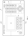
- FIG 1 shows an embodiment, in top plan view of a keypad assembly 10 that incorporates a keypad with an overlay for dissipation of electrostatic charges.
- the keypad illustrated here is only one example of implementing the inventive overlay, which due to their transparent nature, will not be readily noticeable to a user, although some of the features will become apparent to a user as the overlay approaches the end of its useful life and provides visual evidence that the overlay needs to be replaced. While the depicted embodiment of the keypad assembly 10 shows a typical selection and arrangement of keypad elements, it will be readily understood that other selections and arrangements of the keypad elements are possible while still being an effective implementation of the inventive concept, as the overlay itself has a very passive, but effective, role in the operation of the keypad assembly 10.
- the minimal set of elements would include at least one display element 12, depicted here as a screen, and a plurality of data entry elements, such as an on/off button 14, a numeric keypad 16 with buttons for the numerals 0 through 9, a set 18 of four directional arrows with an "entry” button arranged in the middle thereof, and a plurality of functional buttons 20.
- the functional portions of the keypad lie below the overlay itself, which will be designated by reference number 30 in those figures.
- the overlay 30 is based on and receives its structural basis from an overlay substrate 32 that is generally planar with a top side and a back side.
- the top side of the overlay substrate 32 is the right side thereof and the back side is the left side thereof.
- a plurality of layers of inks and coatings are applied to these top and back sides.
- the overlay substrate 32 is the thickest portion of the overlay 30. It is formed of a transparent polymeric material, with polyethylene terephthalate (PET) being a preferred material.
- PET polyethylene terephthalate
- An exemplary overlay substrate 32 is a textured hardcoat polyester film sold commercially under the trademark AUTOTEX by MacDermid Autotype Inc.
- Critical to the functionality of the overlay 30 is a plurality of vias 60 that are formed in the overlay substrate 32. Several of these vias 60 are seen in Fig.2 . Each via 60 is precisely sized and arranged on the substrate 32, according to the predetermined layout of the display element and the data entry elements of a particular keypad for which the overlay 30 is provided. These vias 60 will be discussed below in relation to Figs. 4-6 .
- a pad of conductive ink 34 is applied to the top side of overlay substrate 32, in a manner that allows the ink to flow into the vias from the top side, at least partially filling them.
- An appropriate pad could be CLEVIOS F DX 2/X-L 2K, commercially available from Heraeus GmbH & Co.
- a pattern 36 of conductive silver paste is selectively applied atop the conductive ink 36.
- the specifics of the selective pattern 36 will be better understood with relation to Figs 4 and 6 , but for now, it is noted that the silver paste is positioned atop the vias, generally in interconnected linear runs.
- Conductive silver paste is known in the industry and a typical paste would be ACHESON 8208.
- a pattern 38 of colored ink is applied atop the pattern 36 of conductive silver paste to obscure visibility of the pattern 36 when viewed from the top of the keypad assembly.
- this pattern 38 comprises the interconnected linear elements that set out borders around the display element 12 and the various data entry elements 14, 16, 18, 20.
- the color ink is commonly used in the industry and readily known to one of skill.
- One example would be a JUJO 900 SERIES ink.
- the next layer outwardly from the top side of the overlay substrate 32 is a coating 40 of a conductive polymeric material.
- This coating provides the primary surface that is touched by a user, so it is a static-dissipative material.
- a material that is suitable for this coating 40 is a protective CLEVIOS hardcoat, commercially available from Heraeus GmbH & Co. KG, where CLEVIOS is the registered trademark for its conductive polymer chemistry.
- CLEVIOS PEDOT/PSS is a complex of a substituted polythiophene and an anion that offers a conductivity in the range of 1000 Siemens per centimeter (S/cm). It is available in an extremely thin, electrically conductive coating.
- the material has good thermal and ultraviolet stability.
- CLEVIOS as an antistatic coating useful for protecting integrated circuit packaging trays to prevent damage of sensitive electronic components from ESD.
- the website indicates that many plastics, including polycarbonates, polyethylene, polyethylene terephthalate, polyamide and polypropylene, can be coated with CLEVIOS.
- the last layer on the top side of the overlay substrate 32 is a thin insulating layer of optical ink 42. It is preferably applied only on the area projected by the display element 12 onto the static-dissipative coating 40. While the optical ink 42 is applied to clarify the display window, it does re-introduce the risk of charges collecting.
- a suitable method of mitigating charge collection in this area is to minimize the surface area of the insulating layer or to introduce a staggered grid of holes to encourage a low energy-flash over discharge before an accumulation capable of ignition can occur.
- An exemplary material for this layer is a WINDOTEX material as available from MacDermid Autotype Inc.
- a pattern 46 of conductive silver paste is selectively applied onto the back side, outwardly from the color ink layer.
- the selective pattern 46 will effectively mirror the conductive silver paste pattern 36, as will be seen further in the description of Figs. 5 and 6 .
- the conductive silver paste 46 can be that sold as ACHESON 8208.
- electrostatic charges arising on the top side of the overlay substrate 32 will migrate to the conductive silver paste 36, drain through a via 60 to the bottom side of the overlay substrate and be collected by the conductive silver paste 46.
- the interconnectivity of the lengths of silver paste 46 will move the charges to a grounded tab.
- an adhesive layer 48 is provided, so that the overlay 30, with its various layers, can be affixed to the keypad 70, which is now described.
- the overlay 30 is intended to be able to be readily replaced as it is expended through use.
- the adhesive is preferably a double-sided pressure-sensitive adhesive on a polymeric film. Notably, no adhesive is applied to the area representing the display area.
- a further adhesive layer 72 which is used to affix the keypad assembly 10 to a metal equipment enclosure (not shown) that contains the electronics for the device.
- Fig. 3 shows a transparent keypad spacer 74, through which the display element 12 is viewed.
- a polymeric sheet, especially a polycarbonate material, is typically used as the keypad spacer 74.
- an upper layer 76 of the keypad is a polymeric layer, typically a polyethylene terephthalate such as LUMIRROR T60 polyester sold by Toray Industries Ltd.
- the upper layer 76 is selectively cut to facilitate physical movement of the metal domes 78, one of which is below each of the data entry elements.
- the metal domes 78, as well as an interlayer 80 that comprises an adhesive are positioned between the upper layer 76 and a circuit layer 82, which is typically of the same composition as the upper layer 76.
- a further adhesive layer 84 affixes the circuit layer 82 to a circuit spacer layer 86.
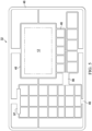
- Figure 4 is a top plan view of the overlay substrate 32, and is presented here to show the location of the vias 60 that are formed in the overlay substrate.
- structures such as the display element 12, the on/off button 14, the numeric keypad 16, the set of directional arrows 18 and the set of functional buttons 20 are recognizable from Fig. 1 .
- a plurality of dashed lines are used to portray borders that divide the surface area of the overlay substrate 32 into enclosed zones. Due to the coatings atop the overlay substrate 32, the "areas" are really “volumes,” although the depth is quite small relative to the width and breadth. Accordingly, there are “enclosed volumes” rather than enclosed areas or zones.
- the vias 60 are depicted as dots along the dashed lines.
- One of the dashed lines is provided around the periphery of the overlay substrate 32.
- a plurality of smaller volumes are Type II enclosed volumes 92. These encompass volumes that are subject to being touched by a user, but which do not have an underlying data entry element 14, 16, 18 or 20.
- a plurality of rectangular encompassed volumes are the Type III volumes 94. Each of these has one underlying data entry element.
- These Type III enclosed volumes 94 are considered to be the areas at highest risk for an electrostatic charge to arise.
- the series of dashed lines in Fig. 4 clearly depict a pattern for laying down the layer 36 of conductive silver paste seen in side sectional view in Fig. 2 , as well as a pattern for covering the conductive silver paste layer with layer of color ink 38.
- the inventive concept it is preferred in the inventive concept to divide the surface area of the overlay substrate 32, and especially the Type III zones 94, so that the surface area is less than 500 mm2.
- the maximum unprotected area of an insulating material is 500mm2.
- the color ink layer 38 that covers the conductive silver paste layer 36 provides a watermark feature, which enables the user to visually detect when the conductive polymeric coating 40 has been damaged or worn off, to the extent that the overlay needs to be replaced. By framing the Type III zones 94 using the conductive silver paste, damaged areas will not exceed the 500mm2 required per the standard.
- a preferred color ink 38 is an ink from the 9000 Series PET, commercially-available from Jujo Chemical Co. Ltd. of Japan. This ink is suitable for high-speed printing with excellent adhesion on PET.
- the vias 60 are precisely sized and arranged on the overlay substrate 32. Each via 60 is cut into the substrate 32, preferably by a laser, providing a precisely positioned and sized conduit between the top and bottom sides of the substrate, for transmission of electrostatic charges. When filled with conductive ink, as will be described, the vias 60 provide a grounding solution, draining charges from the top side to an inner conductive collector surface on the bottom side of the substrate. From there, a conductive tab connects the inner conductive collector surface to a metal equipment enclosure of the device. A wire connects the equipment enclosure to earth ground, thus preventing charge build-up on the plastic overlay outer surface. The vias are small and not readily noticeable and thus do not detract from the overlay appearance.
- Figure 5 shows a bottom plan view of a bottom surface of the overlay substrate 32. Note that the display area 12 is moved to the right side of the pad arrangement, due to the view from the bottom side. This illustrates a few different points. One point is how the conductive silver paste layer 46 on the bottom side mirrors the pattern of conductive silver paste on the top side, showing how the vias communicate and interconnect these conductive layers. The second point is how the pattern of the silver paste layer 46 has at least one widened portion 96 that is used to connect the silver paste layer 46 to a grounding pad or wire. A second widened portion 97 is also shown.
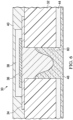
- Figure 6 is an enlarged side sectional view of the overlay 30 focusing on a single via 60, formed in nonconductive overlay substrate 32.
- placement of conductive ink 34 on the top side of the overlay substrate 32 allows the conductive ink 34 to flow into the via 60, at least partially filling it.
- color ink layer 44 is applied to the bottom side of overlay substrate 32 before the vias 60 are formed, it does not flow into the vias, but when the conductive paste layer 46 is applied to the bottom side, it completes the filling of the via 60, so that an electrical communication is established between conductive paste layers 36, 46.
- the shape and location of an interface between conductive paste layers 36, 46 can vary, and the illustrated interface is only exemplary.
- Color ink layer 38 covers conductive paste layer 36, so that the former is only visible if the color ink layer has been damaged or worn.
- the static-dissipative conducting layer 40 is in communication, through conductive ink 34 with conductive paste layer the conductive paste layer 36. Charges arising in any of the zones 90, 92, 94 are thereby able to freely flow from the top side of the overlay substrate 32 to the conductive paste layer 46 on the bottom side. From there, these charges flow by their potential difference to the ground connection provided by the widened portion 96, shown in Fig. 5 .
- FIG. 7 is a top plan view of the rear adhesive layer 48 of the overlay assembly 30.
- Pressure sensitive adhesive is distributed across the entire top surface of rear adhesive layer 48, typically a material provided by 3M as product 9672LE, except at cutouts 98, 100, 102. Cutout 98 corresponds to the display area, and cutouts 100, 102 correspond to widened portions 96 and 97.
Landscapes
- Engineering & Computer Science (AREA)
- Microelectronics & Electronic Packaging (AREA)
- General Engineering & Computer Science (AREA)
- Theoretical Computer Science (AREA)
- Human Computer Interaction (AREA)
- Physics & Mathematics (AREA)
- General Physics & Mathematics (AREA)
- Push-Button Switches (AREA)
Claims (14)
- Baugruppe (10) zum Schützen einer Kunststofftastatur, die Dateneingabeelemente (14, 16, 18, 20) und mindestens ein Anzeigeelement (12), aufweist, vor elektrostatische Entladung, wobei die Baugruppe (10) Folgendes umfasst:ein Überlagerungssubstrat (32), das eine Oberseite und eine Rückseite aufweist, wobei das Überlagerungssubstrat (32) ferner eine Vielzahl von genau positionierten Durchgängen (60) aufweist, die durch dieses hindurch ausgebildet ist, wobei die Oberseite eine Oberfläche aufweist, die mit einer statisch ableitenden Schicht aus einem leitfähigen Polymer (40) beschichtet ist, und die Rückseite eine Rückfläche aufweist, die mit mindestens einer farbigen Tintenschicht (44) bedruckt ist, wobei die mindestens eine farbige Tintenschicht (44) eine Vielzahl von alphanumerischen (16) und bildlichen Elementen (14, 18, 20) der Tastatur darstellt; undeine elektrisch leitfähige Anordnung (30), die auf dem Überlagerungssubstrat (32) angeordnet ist, um elektrostatische Ladungen an der Oberseite zu sammeln, die elektrostatischen Ladungen durch die Vielzahl von Durchgängen (60) auf die Rückseite zu übertragen und die übertragenen elektrostatischen Ladungen an Masse zu entladen,dadurch gekennzeichnet, dass
die elektrisch leitfähige Anordnung (30) Folgendes umfasst:mindestens ein erstes leitfähiges Gitter (34), das auf die Oberfläche des Überlagerungssubstrats (32) unterhalb der Schicht aus leitfähigem Polymer (40) gedruckt ist, wobei das mindestens eine erste leitfähige Gitter (34) die Oberfläche in eine Vielzahl von umgebenen Bereichen unterteilt, wobei jeder davon gleich einer vorbestimmten Größe oder kleiner als diese ist, wobei jedes der ersten leitfähigen Gitter (34) eine Vielzahl von Knotenpunkten umfasst, wobei jeder Knotenpunkt oben auf einem entsprechenden der Vielzahl von genau positionierten Durchgängen (60) positioniert ist und sich in diesen erstreckt;mindestens ein zweites leitfähiges Gitter (48), das auf die Rückfläche des Überlagerungssubstrats (32) unter der mindestens einen farbigen Tintenschicht (44) gedruckt ist, sodass jedes zweite leitfähige Gitter (48) in Größe und Form einem der ersten leitfähigen Gitter (34) entspricht, wobei jedes der zweiten leitfähigen Gitter (48) eine Vielzahl von Knotenpunkten umfasst, wobei jeder Knotenpunkt unter einem entsprechenden der Vielzahl von genau positionierten Durchgängen (60) positioniert ist und sich in diesen erstreckt; undmindestens eine leitfähige Verbindung (96, 97), die jedes zweite leitfähige Gitter (48) mit Masse verbindet. - Baugruppe nach Anspruch 1, wobei jedes der ersten leitfähigen Gitter (34) und der zweiten leitfähigen Gitter (48) Längen einer leitfähigen Paste (36, 46) umfasst, die auf das Überlagerungssubstrat (32) gedruckt ist.
- Baugruppe nach Anspruch 2, wobei eine farbige Tintenschicht (38) auf die Längen der leitfähigen Paste (36) in jedem der ersten leitfähigen Gitter (34) aufgebracht ist.
- Baugruppe nach Anspruch 3, wobei die Knotenpunkte jedes der ersten leitfähigen Gitter (34) Folgendes umfassen:einen Stopfen aus einem leitfähigen Polymer, der von der Oberseite des Überlagerungssubstrats (32) aus auf jeden der genau positionierten Durchgänge (60) aufgebracht ist, wobei der Stopfen einen sich in den Durchgang erstreckenden Körperabschnitt und einen Flanschabschnitt und einen Durchmesser aufweist, der größer als ein Durchmesser der Durchgänge ist, der sich auf die Oberseite des Überlagerungssubstrats (32) erstreckt;eine Länge der leitfähigen Paste (36), die auf den Stopfen aufgebracht ist; undeine Länge der farbigen Tinte (38), die auf die Länge der leitfähigen Paste (36) aufgebracht ist.
- Baugruppe nach einem der Ansprüche 2 bis 4, wobei die Knotenpunkte jedes der zweiten leitfähigen Gitter (48) einen Abschnitt der leitfähigen Paste (46) umfassen, der sich von der Unterseite des Überlagerungssubstrats (32) in den Durchgang (60) erstreckt, dem er zugeordnet ist, um einen elektrischen Kontakt mit dem entsprechenden Knotenpunkt des ersten leitfähigen Gitters (34) herzustellen.
- Baugruppe nach Anspruch 1, wobei das Überlagerungssubstrat (32) ein nicht-leitfähiges Polymer umfasst.
- Baugruppe nach Anspruch 6, wobei das nicht-leitfähige Polymer eine Polyethylenterephthalat(PET)-Schicht ist.
- Baugruppe nach Anspruch 1, wobei die statisch ableitende Beschichtung transparent ist.
- Baugruppe nach Anspruch 8, wobei die statisch ableitende Beschichtung eine Transparenz Y von bis zu 90 % bei d = 100 nm aufweist.
- Baugruppe nach Anspruch 8, wobei die statisch ableitende Beschichtung ein Komplex aus einem substituierten Polythiophen und einem Anion ist, der eine Leitfähigkeit im Bereich von 1000 Siemens pro Zentimeter (S/cm) bietet.
- Baugruppe nach Anspruch 1, wobei eines der Vielzahl von ersten leitfähigen Gittern (34) ein leitfähiges Gitter mit Durchgängen (60) ist, die um einen Umfang des Überlagerungssubstrats (32) herum positioniert sind.
- Baugruppe nach Anspruch 1 oder Anspruch 11, wobei ein Bereich, der jedem Dateneingabeelement (14, 16, 18, 20) der Tastatur entspricht, durch mindestens eines der ersten leitfähigen Gitter (34) umgeben ist.
- Elektronische Vorrichtung zur Dateneingabe und -anzeige, umfassend:ein Gehäuse;eine Tastatur, die zur Dateneingabe und -anzeige geeignet ist und an dem Gehäuse montiert ist; undeine Baugruppe (10) nach Anspruch 1, die oben auf der Tastatur angeordnet und durch das Gehäuse in ihrer Position gesichert ist, wobei die Baugruppe (10) geeignet ist, elektrostatische Ladungen, die durch Verwendung der Tastatur entstehen, abzuleiten.
- Elektronische Vorrichtung nach Anspruch 13, wobei:das Gehäuse metallisch ist; unddurch die Baugruppe (10) abgeleitete elektrostatische Ladungen zu dem Gehäuse entladen werden.
Applications Claiming Priority (1)
| Application Number | Priority Date | Filing Date | Title |
|---|---|---|---|
| CN202110133181.5A CN114816078A (zh) | 2021-01-29 | 2021-01-29 | 具有静电放电耗散的键盘覆盖物 |
Publications (2)
| Publication Number | Publication Date |
|---|---|
| EP4037446A1 EP4037446A1 (de) | 2022-08-03 |
| EP4037446B1 true EP4037446B1 (de) | 2024-08-21 |
Family
ID=80685156
Family Applications (1)
| Application Number | Title | Priority Date | Filing Date |
|---|---|---|---|
| EP22154094.1A Active EP4037446B1 (de) | 2021-01-29 | 2022-01-28 | Tastaturüberlagerung mit ableitung elektrostatischer entladung |
Country Status (3)
| Country | Link |
|---|---|
| US (2) | US12035449B2 (de) |
| EP (1) | EP4037446B1 (de) |
| CN (1) | CN114816078A (de) |
Family Cites Families (26)
| Publication number | Priority date | Publication date | Assignee | Title |
|---|---|---|---|---|
| DD156858A1 (de) | 1981-03-12 | 1982-09-22 | Klaus Wolf | Schalter mit fluessigkeitskontakt |
| JP3151553B2 (ja) | 1996-11-29 | 2001-04-03 | 帝国通信工業株式会社 | キートップ板及びその製造方法 |
| SE513069C2 (sv) * | 1997-03-03 | 2000-07-03 | Ericsson Telefon Ab L M | Skydd mot elektrostatisk urladdning i en portabel kommunikationsapparat |
| JP4037483B2 (ja) | 1997-04-14 | 2008-01-23 | ポリマテック株式会社 | シート状キートップおよびその製造方法 |
| JP3102854B2 (ja) | 1997-08-08 | 2000-10-23 | 信越ポリマー株式会社 | 照光式押釦スイッチ用カバー部材およびその製造方法 |
| US5807002A (en) | 1997-08-26 | 1998-09-15 | Silitek Corporation | Super-thin plastic key |
| USD431482S (en) | 1999-04-26 | 2000-10-03 | Mettler-Tolodo GmbH | Terminal for weighing apparatus |
| JP2001084863A (ja) | 1999-09-13 | 2001-03-30 | Polymatech Co Ltd | シート状キートップ |
| KR100619852B1 (ko) | 2004-04-30 | 2006-09-08 | 엘지전자 주식회사 | 이동통신 단말기 본체 |
| US7567419B2 (en) * | 2005-06-10 | 2009-07-28 | Kyocera Wireless Corp. | Apparatus, system, and method for electrostatic discharge protection |
| WO2007084569A2 (en) * | 2006-01-20 | 2007-07-26 | Plextronics, Inc. | Electrostatic coatings and articles comprising polythiophenes |
| US7541939B2 (en) | 2007-03-15 | 2009-06-02 | Apple Inc. | Mounted shock sensor |
| USD582308S1 (en) | 2007-08-23 | 2008-12-09 | Kabushiki Kaisha Toshiba | Remote controller for body weight and body composition measuring machine |
| DE102008053351B3 (de) * | 2008-10-27 | 2010-08-05 | Gigaset Communications Gmbh | Bedienfeld für ein Tastaturmodul, Tastaturmodul und Verfahren zu deren Herstellung |
| TWD137268S1 (zh) | 2009-03-02 | 2010-10-11 | 歐姆龍健康醫療事業股份有限公司 | 內臟脂肪測定器 |
| CA2715412C (en) | 2010-04-02 | 2017-07-18 | Ovs, Inc. | Electronic weighing system |
| GB2482310B (en) | 2010-07-28 | 2013-04-10 | Illinois Tool Works | Printer device |
| JP5807976B2 (ja) | 2011-11-04 | 2015-11-10 | 株式会社エー・アンド・デイ | 計量装置用データロガー |
| USD672262S1 (en) | 2012-01-11 | 2012-12-11 | Illinois Tool Works Inc. | Control panel for weight measuring device |
| US9347820B2 (en) | 2012-11-20 | 2016-05-24 | Carematix, Inc. | Body weight measuring techniques |
| US10759145B2 (en) * | 2015-10-23 | 2020-09-01 | Hp Indigo B.V. | Laminates |
| US10194514B2 (en) * | 2015-11-11 | 2019-01-29 | Rockwell Automation Technologies, Inc. | Electrostatic charge grounding for human machine interface equipment |
| USD813067S1 (en) | 2016-03-25 | 2018-03-20 | Illinois Tool Works Inc. | Control panel for a bench scale weighing device |
| USD830212S1 (en) | 2016-03-25 | 2018-10-09 | Illinois Tool Works Inc. | Control panel for a bench scale weighing device |
| KR101922185B1 (ko) | 2017-04-21 | 2018-11-26 | 주식회사 썬웨이커뮤니케이션코리아 | 휴대용 전자 부품 및 그 제조 방법 |
| USD856179S1 (en) | 2018-01-15 | 2019-08-13 | Jiangyin Suofei Electronic Technology Co., Ltd. | Scale controller |
-
2021
- 2021-01-29 CN CN202110133181.5A patent/CN114816078A/zh active Pending
-
2022
- 2022-01-27 US US17/585,893 patent/US12035449B2/en active Active
- 2022-01-28 EP EP22154094.1A patent/EP4037446B1/de active Active
- 2022-12-12 US US29/862,706 patent/USD1023806S1/en active Active
Also Published As
| Publication number | Publication date |
|---|---|
| US20220248521A1 (en) | 2022-08-04 |
| USD1023806S1 (en) | 2024-04-23 |
| CN114816078A (zh) | 2022-07-29 |
| EP4037446A1 (de) | 2022-08-03 |
| US12035449B2 (en) | 2024-07-09 |
Similar Documents
| Publication | Publication Date | Title |
|---|---|---|
| US8421755B2 (en) | Capacitive touch sensor with integral EL backlight | |
| KR101179530B1 (ko) | 터치 패널 스택업 | |
| US9116589B2 (en) | Single-layer projected capacitive touch panel and method of manufacturing the same | |
| US9921682B2 (en) | Touch panel having high resistance to static electricity | |
| TWI550458B (zh) | 觸控式面板 | |
| EP2597551B1 (de) | Berührungstafel mit Umrandung ohne Farbunterschied und Herstellungsverfahren dafür | |
| US20050237439A1 (en) | Touch panel | |
| CN109947305B (zh) | 触摸面板及其制备方法、触摸显示装置 | |
| TWI657365B (zh) | Wiring body, wiring board, and touch detector | |
| KR100836749B1 (ko) | 발광형 정전용량 터치센서 | |
| KR20150138719A (ko) | 정전기 방지를 위한 정전기 방지 전극이 배선된 터치 패널 | |
| CN112506371A (zh) | 触控基板和触控显示装置 | |
| CN114326189B (zh) | 显示装置及显示装置的制造方法 | |
| CN105988631A (zh) | 触控面板及其制作方法 | |
| US12035449B2 (en) | Keypad overlay with electrostatic discharge dissipation | |
| KR102105607B1 (ko) | 정전 용량식 센서 | |
| CN106155387B (zh) | 触控面板及其制造方法 | |
| US20160147323A1 (en) | Touch control panel structure and method of manufacturing the same | |
| JP2014215682A (ja) | 静電容量型入力装置及びその製造方法 | |
| CN102654797A (zh) | 触控面板 | |
| EP4049120B1 (de) | Cursorsteuerungsvorrichtung mit gedrucktem berührungssensor | |
| CN223219123U (zh) | 一种保护壳及其触感连接器 | |
| EP3528100B1 (de) | Berührungsbildschirm | |
| KR100789587B1 (ko) | 양면 정전기 방지층을 구비한 유연성 전계발광소자 | |
| CN114077331A (zh) | 触控面板及触控设备 |
Legal Events
| Date | Code | Title | Description |
|---|---|---|---|
| PUAI | Public reference made under article 153(3) epc to a published international application that has entered the european phase |
Free format text: ORIGINAL CODE: 0009012 |
|
| STAA | Information on the status of an ep patent application or granted ep patent |
Free format text: STATUS: THE APPLICATION HAS BEEN PUBLISHED |
|
| AK | Designated contracting states |
Kind code of ref document: A1 Designated state(s): AL AT BE BG CH CY CZ DE DK EE ES FI FR GB GR HR HU IE IS IT LI LT LU LV MC MK MT NL NO PL PT RO RS SE SI SK SM TR |
|
| STAA | Information on the status of an ep patent application or granted ep patent |
Free format text: STATUS: REQUEST FOR EXAMINATION WAS MADE |
|
| 17P | Request for examination filed |
Effective date: 20230127 |
|
| RBV | Designated contracting states (corrected) |
Designated state(s): AL AT BE BG CH CY CZ DE DK EE ES FI FR GB GR HR HU IE IS IT LI LT LU LV MC MK MT NL NO PL PT RO RS SE SI SK SM TR |
|
| GRAP | Despatch of communication of intention to grant a patent |
Free format text: ORIGINAL CODE: EPIDOSNIGR1 |
|
| STAA | Information on the status of an ep patent application or granted ep patent |
Free format text: STATUS: GRANT OF PATENT IS INTENDED |
|
| RIC1 | Information provided on ipc code assigned before grant |
Ipc: G06F 3/039 20130101ALI20240425BHEP Ipc: H05K 9/00 20060101AFI20240425BHEP |
|
| INTG | Intention to grant announced |
Effective date: 20240510 |
|
| GRAS | Grant fee paid |
Free format text: ORIGINAL CODE: EPIDOSNIGR3 |
|
| GRAA | (expected) grant |
Free format text: ORIGINAL CODE: 0009210 |
|
| STAA | Information on the status of an ep patent application or granted ep patent |
Free format text: STATUS: THE PATENT HAS BEEN GRANTED |
|
| AK | Designated contracting states |
Kind code of ref document: B1 Designated state(s): AL AT BE BG CH CY CZ DE DK EE ES FI FR GB GR HR HU IE IS IT LI LT LU LV MC MK MT NL NO PL PT RO RS SE SI SK SM TR |
|
| REG | Reference to a national code |
Ref country code: GB Ref legal event code: FG4D |
|
| REG | Reference to a national code |
Ref country code: CH Ref legal event code: EP |
|
| REG | Reference to a national code |
Ref country code: DE Ref legal event code: R096 Ref document number: 602022005383 Country of ref document: DE |
|
| REG | Reference to a national code |
Ref country code: IE Ref legal event code: FG4D Ref country code: NL Ref legal event code: FP |
|
| REG | Reference to a national code |
Ref country code: LT Ref legal event code: MG9D |
|
| PG25 | Lapsed in a contracting state [announced via postgrant information from national office to epo] |
Ref country code: NO Free format text: LAPSE BECAUSE OF FAILURE TO SUBMIT A TRANSLATION OF THE DESCRIPTION OR TO PAY THE FEE WITHIN THE PRESCRIBED TIME-LIMIT Effective date: 20241121 |
|
| REG | Reference to a national code |
Ref country code: AT Ref legal event code: MK05 Ref document number: 1716876 Country of ref document: AT Kind code of ref document: T Effective date: 20240821 |
|
| PG25 | Lapsed in a contracting state [announced via postgrant information from national office to epo] |
Ref country code: FI Free format text: LAPSE BECAUSE OF FAILURE TO SUBMIT A TRANSLATION OF THE DESCRIPTION OR TO PAY THE FEE WITHIN THE PRESCRIBED TIME-LIMIT Effective date: 20240821 Ref country code: PT Free format text: LAPSE BECAUSE OF FAILURE TO SUBMIT A TRANSLATION OF THE DESCRIPTION OR TO PAY THE FEE WITHIN THE PRESCRIBED TIME-LIMIT Effective date: 20241223 Ref country code: PL Free format text: LAPSE BECAUSE OF FAILURE TO SUBMIT A TRANSLATION OF THE DESCRIPTION OR TO PAY THE FEE WITHIN THE PRESCRIBED TIME-LIMIT Effective date: 20240821 Ref country code: GR Free format text: LAPSE BECAUSE OF FAILURE TO SUBMIT A TRANSLATION OF THE DESCRIPTION OR TO PAY THE FEE WITHIN THE PRESCRIBED TIME-LIMIT Effective date: 20241122 |
|
| PG25 | Lapsed in a contracting state [announced via postgrant information from national office to epo] |
Ref country code: BG Free format text: LAPSE BECAUSE OF FAILURE TO SUBMIT A TRANSLATION OF THE DESCRIPTION OR TO PAY THE FEE WITHIN THE PRESCRIBED TIME-LIMIT Effective date: 20240821 |
|
| PG25 | Lapsed in a contracting state [announced via postgrant information from national office to epo] |
Ref country code: LV Free format text: LAPSE BECAUSE OF FAILURE TO SUBMIT A TRANSLATION OF THE DESCRIPTION OR TO PAY THE FEE WITHIN THE PRESCRIBED TIME-LIMIT Effective date: 20240821 |
|
| PG25 | Lapsed in a contracting state [announced via postgrant information from national office to epo] |
Ref country code: AT Free format text: LAPSE BECAUSE OF FAILURE TO SUBMIT A TRANSLATION OF THE DESCRIPTION OR TO PAY THE FEE WITHIN THE PRESCRIBED TIME-LIMIT Effective date: 20240821 Ref country code: IS Free format text: LAPSE BECAUSE OF FAILURE TO SUBMIT A TRANSLATION OF THE DESCRIPTION OR TO PAY THE FEE WITHIN THE PRESCRIBED TIME-LIMIT Effective date: 20241221 |
|
| PG25 | Lapsed in a contracting state [announced via postgrant information from national office to epo] |
Ref country code: HR Free format text: LAPSE BECAUSE OF FAILURE TO SUBMIT A TRANSLATION OF THE DESCRIPTION OR TO PAY THE FEE WITHIN THE PRESCRIBED TIME-LIMIT Effective date: 20240821 |
|
| PG25 | Lapsed in a contracting state [announced via postgrant information from national office to epo] |
Ref country code: ES Free format text: LAPSE BECAUSE OF FAILURE TO SUBMIT A TRANSLATION OF THE DESCRIPTION OR TO PAY THE FEE WITHIN THE PRESCRIBED TIME-LIMIT Effective date: 20240821 Ref country code: RS Free format text: LAPSE BECAUSE OF FAILURE TO SUBMIT A TRANSLATION OF THE DESCRIPTION OR TO PAY THE FEE WITHIN THE PRESCRIBED TIME-LIMIT Effective date: 20241121 |
|
| PG25 | Lapsed in a contracting state [announced via postgrant information from national office to epo] |
Ref country code: RS Free format text: LAPSE BECAUSE OF FAILURE TO SUBMIT A TRANSLATION OF THE DESCRIPTION OR TO PAY THE FEE WITHIN THE PRESCRIBED TIME-LIMIT Effective date: 20241121 Ref country code: PT Free format text: LAPSE BECAUSE OF FAILURE TO SUBMIT A TRANSLATION OF THE DESCRIPTION OR TO PAY THE FEE WITHIN THE PRESCRIBED TIME-LIMIT Effective date: 20241223 Ref country code: PL Free format text: LAPSE BECAUSE OF FAILURE TO SUBMIT A TRANSLATION OF THE DESCRIPTION OR TO PAY THE FEE WITHIN THE PRESCRIBED TIME-LIMIT Effective date: 20240821 Ref country code: NO Free format text: LAPSE BECAUSE OF FAILURE TO SUBMIT A TRANSLATION OF THE DESCRIPTION OR TO PAY THE FEE WITHIN THE PRESCRIBED TIME-LIMIT Effective date: 20241121 Ref country code: LV Free format text: LAPSE BECAUSE OF FAILURE TO SUBMIT A TRANSLATION OF THE DESCRIPTION OR TO PAY THE FEE WITHIN THE PRESCRIBED TIME-LIMIT Effective date: 20240821 Ref country code: IS Free format text: LAPSE BECAUSE OF FAILURE TO SUBMIT A TRANSLATION OF THE DESCRIPTION OR TO PAY THE FEE WITHIN THE PRESCRIBED TIME-LIMIT Effective date: 20241221 Ref country code: HR Free format text: LAPSE BECAUSE OF FAILURE TO SUBMIT A TRANSLATION OF THE DESCRIPTION OR TO PAY THE FEE WITHIN THE PRESCRIBED TIME-LIMIT Effective date: 20240821 Ref country code: GR Free format text: LAPSE BECAUSE OF FAILURE TO SUBMIT A TRANSLATION OF THE DESCRIPTION OR TO PAY THE FEE WITHIN THE PRESCRIBED TIME-LIMIT Effective date: 20241122 Ref country code: FI Free format text: LAPSE BECAUSE OF FAILURE TO SUBMIT A TRANSLATION OF THE DESCRIPTION OR TO PAY THE FEE WITHIN THE PRESCRIBED TIME-LIMIT Effective date: 20240821 Ref country code: ES Free format text: LAPSE BECAUSE OF FAILURE TO SUBMIT A TRANSLATION OF THE DESCRIPTION OR TO PAY THE FEE WITHIN THE PRESCRIBED TIME-LIMIT Effective date: 20240821 Ref country code: BG Free format text: LAPSE BECAUSE OF FAILURE TO SUBMIT A TRANSLATION OF THE DESCRIPTION OR TO PAY THE FEE WITHIN THE PRESCRIBED TIME-LIMIT Effective date: 20240821 Ref country code: AT Free format text: LAPSE BECAUSE OF FAILURE TO SUBMIT A TRANSLATION OF THE DESCRIPTION OR TO PAY THE FEE WITHIN THE PRESCRIBED TIME-LIMIT Effective date: 20240821 |
|
| PG25 | Lapsed in a contracting state [announced via postgrant information from national office to epo] |
Ref country code: SM Free format text: LAPSE BECAUSE OF FAILURE TO SUBMIT A TRANSLATION OF THE DESCRIPTION OR TO PAY THE FEE WITHIN THE PRESCRIBED TIME-LIMIT Effective date: 20240821 Ref country code: DK Free format text: LAPSE BECAUSE OF FAILURE TO SUBMIT A TRANSLATION OF THE DESCRIPTION OR TO PAY THE FEE WITHIN THE PRESCRIBED TIME-LIMIT Effective date: 20240821 Ref country code: RO Free format text: LAPSE BECAUSE OF FAILURE TO SUBMIT A TRANSLATION OF THE DESCRIPTION OR TO PAY THE FEE WITHIN THE PRESCRIBED TIME-LIMIT Effective date: 20240821 |
|
| PG25 | Lapsed in a contracting state [announced via postgrant information from national office to epo] |
Ref country code: EE Free format text: LAPSE BECAUSE OF FAILURE TO SUBMIT A TRANSLATION OF THE DESCRIPTION OR TO PAY THE FEE WITHIN THE PRESCRIBED TIME-LIMIT Effective date: 20240821 |
|
| PG25 | Lapsed in a contracting state [announced via postgrant information from national office to epo] |
Ref country code: CZ Free format text: LAPSE BECAUSE OF FAILURE TO SUBMIT A TRANSLATION OF THE DESCRIPTION OR TO PAY THE FEE WITHIN THE PRESCRIBED TIME-LIMIT Effective date: 20240821 |
|
| PG25 | Lapsed in a contracting state [announced via postgrant information from national office to epo] |
Ref country code: SK Free format text: LAPSE BECAUSE OF FAILURE TO SUBMIT A TRANSLATION OF THE DESCRIPTION OR TO PAY THE FEE WITHIN THE PRESCRIBED TIME-LIMIT Effective date: 20240821 |
|
| REG | Reference to a national code |
Ref country code: DE Ref legal event code: R097 Ref document number: 602022005383 Country of ref document: DE |
|
| PLBE | No opposition filed within time limit |
Free format text: ORIGINAL CODE: 0009261 |
|
| STAA | Information on the status of an ep patent application or granted ep patent |
Free format text: STATUS: NO OPPOSITION FILED WITHIN TIME LIMIT |
|
| 26N | No opposition filed |
Effective date: 20250522 |
|
| PG25 | Lapsed in a contracting state [announced via postgrant information from national office to epo] |
Ref country code: SE Free format text: LAPSE BECAUSE OF FAILURE TO SUBMIT A TRANSLATION OF THE DESCRIPTION OR TO PAY THE FEE WITHIN THE PRESCRIBED TIME-LIMIT Effective date: 20240821 |
|
| PG25 | Lapsed in a contracting state [announced via postgrant information from national office to epo] |
Ref country code: MC Free format text: LAPSE BECAUSE OF FAILURE TO SUBMIT A TRANSLATION OF THE DESCRIPTION OR TO PAY THE FEE WITHIN THE PRESCRIBED TIME-LIMIT Effective date: 20240821 Ref country code: LU Free format text: LAPSE BECAUSE OF NON-PAYMENT OF DUE FEES Effective date: 20250128 |
|
| PG25 | Lapsed in a contracting state [announced via postgrant information from national office to epo] |
Ref country code: BE Free format text: LAPSE BECAUSE OF NON-PAYMENT OF DUE FEES Effective date: 20250131 |
|
| REG | Reference to a national code |
Ref country code: BE Ref legal event code: MM Effective date: 20250131 |
|
| PG25 | Lapsed in a contracting state [announced via postgrant information from national office to epo] |
Ref country code: IE Free format text: LAPSE BECAUSE OF NON-PAYMENT OF DUE FEES Effective date: 20250128 |
|
| REG | Reference to a national code |
Ref country code: CH Ref legal event code: U11 Free format text: ST27 STATUS EVENT CODE: U-0-0-U10-U11 (AS PROVIDED BY THE NATIONAL OFFICE) Effective date: 20260201 |
|
| PGFP | Annual fee paid to national office [announced via postgrant information from national office to epo] |
Ref country code: NL Payment date: 20260122 Year of fee payment: 5 |
|
| PGFP | Annual fee paid to national office [announced via postgrant information from national office to epo] |
Ref country code: DE Payment date: 20260127 Year of fee payment: 5 |
|
| PGFP | Annual fee paid to national office [announced via postgrant information from national office to epo] |
Ref country code: IT Payment date: 20260123 Year of fee payment: 5 |
|
| PGFP | Annual fee paid to national office [announced via postgrant information from national office to epo] |
Ref country code: FR Payment date: 20260126 Year of fee payment: 5 |
|
| PGFP | Annual fee paid to national office [announced via postgrant information from national office to epo] |
Ref country code: CH Payment date: 20260201 Year of fee payment: 5 |