EP4033552B1 - Struktur zum halten eines supraleitenden drahtes - Google Patents
Struktur zum halten eines supraleitenden drahtes Download PDFInfo
- Publication number
- EP4033552B1 EP4033552B1 EP20866135.5A EP20866135A EP4033552B1 EP 4033552 B1 EP4033552 B1 EP 4033552B1 EP 20866135 A EP20866135 A EP 20866135A EP 4033552 B1 EP4033552 B1 EP 4033552B1
- Authority
- EP
- European Patent Office
- Prior art keywords
- superconducting wire
- superconducting
- holding structure
- layer
- resin material
- Prior art date
- Legal status (The legal status is an assumption and is not a legal conclusion. Google has not performed a legal analysis and makes no representation as to the accuracy of the status listed.)
- Active
Links
Images


Classifications
-
- H—ELECTRICITY
- H01—ELECTRIC ELEMENTS
- H01B—CABLES; CONDUCTORS; INSULATORS; SELECTION OF MATERIALS FOR THEIR CONDUCTIVE, INSULATING OR DIELECTRIC PROPERTIES
- H01B12/00—Superconductive or hyperconductive conductors, cables, or transmission lines
- H01B12/02—Superconductive or hyperconductive conductors, cables, or transmission lines characterised by their form
-
- H—ELECTRICITY
- H10—SEMICONDUCTOR DEVICES; ELECTRIC SOLID-STATE DEVICES NOT OTHERWISE PROVIDED FOR
- H10N—ELECTRIC SOLID-STATE DEVICES NOT OTHERWISE PROVIDED FOR
- H10N60/00—Superconducting devices
- H10N60/80—Constructional details
- H10N60/81—Containers; Mountings
-
- H—ELECTRICITY
- H01—ELECTRIC ELEMENTS
- H01B—CABLES; CONDUCTORS; INSULATORS; SELECTION OF MATERIALS FOR THEIR CONDUCTIVE, INSULATING OR DIELECTRIC PROPERTIES
- H01B1/00—Conductors or conductive bodies characterised by the conductive materials; Selection of materials as conductors
- H01B1/02—Conductors or conductive bodies characterised by the conductive materials; Selection of materials as conductors mainly consisting of metals or alloys
-
- H—ELECTRICITY
- H01—ELECTRIC ELEMENTS
- H01B—CABLES; CONDUCTORS; INSULATORS; SELECTION OF MATERIALS FOR THEIR CONDUCTIVE, INSULATING OR DIELECTRIC PROPERTIES
- H01B12/00—Superconductive or hyperconductive conductors, cables, or transmission lines
- H01B12/02—Superconductive or hyperconductive conductors, cables, or transmission lines characterised by their form
- H01B12/06—Films or wires on bases or cores
Definitions
- the present disclosure relates to a superconducting wire holding structure.
- PTL 1 ( WO 2018 / 181 561 A1 ) describes a superconducting wire material holding structure.
- the superconducting wire holding structure described in PTL 1 includes a holding member and a superconducting wire disposed inside the holding member.
- Document WO 2018 / 078 876 A1 relates to a superconducting wire comprising a main body, a substrate and a cover.
- the main body includes a superconducting material part having a first principle surface and a second principle surface positioned opposite of the first principle surface.
- the substrate supports the second principal surface of the main body.
- the cover is formed at least on the first principle surface of the main body. In the cover, the surface roughness of the center portion of the superconducting wire in the width direction is less than the surface roughness of the edges thereof in the width direction.
- the superconducting wire has a first superconducting wire rod having a first front surface, a first back surface, a first superconducting layer, and first reinforcing layers, and a second superconducting wire rod having a second front surface, a second back surface, a second superconducting layer, and second reinforcing layers; and a connection member joining the first superconducting wire rod to the second superconducting wire rod.
- the first superconducting wire rod has a first edge portion
- the second superconducting wire rod has a second edge portion.
- the first front surface located at the first edge portion is joined by the connection member to the second front surface located at a portion other than the second edge portion, and the second front surface located at the second edge portion is joined by the connection member to the first front surface located at a portion other than the first edge portion.
- Document US 2006 / 073 979 A1 relates to a laminated superconductor wire including a superconductor wire assembly, which includes a first superconductor insert comprising a first high temperature superconductor layer overlaying a first substrate and a second superconductor insert comprising a second high temperature superconductor layer overlaying a second substrate.
- the first and second superconductor inserts are joined together at their respective substrates.
- An electrically conductive structure substantially surrounds the superconductor wire assembly.
- the present disclosure has been made in view of the above-described problems of the prior art. More specifically, the present disclosure provides a superconducting wire holding structure capable of preventing the dew condensation from being generated on the surface of the superconducting wire when the temperature is returned from the cryogenic temperature to the normal temperature.
- the dew condensation can be prevented from being generated on the surface of the superconducting wire when the superconducting wire holding structure is returned from the cryogenic temperature to the normal temperature.
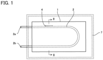
- Fig. 1 is a schematic view illustrating the superconducting wire holding structure of the first embodiment.
- Fig. 2 is a sectional view taken along a line II-II in Fig. 1 .
- the superconducting wire holding structure of the first embodiment includes a holding member 1, a superconducting wire 2, and a filler 3.
- the superconducting wire holding structure of the first embodiment may further include a heater 4.
- Holding member 1 is made of a first material.
- the first material is a resin material (first resin material).
- the first material may be a thermosetting resin material.
- a specific example of the first material is an epoxy resin.
- the first material may be an engineering plastic or a fiber reinforced plastic (FRP).
- Holding member 1 is a member that prevents deformation of the superconducting wire caused by stress due to electromagnetic force applied to a superconducting wire 2.
- Superconducting wire 2 is disposed inside holding member 1.
- Superconducting wire 2 may be curved inside holding member 1.
- Superconducting wire 2 includes a first end 2a and a second end 2b.
- First end 2a and second end 2b are ends in the longitudinal direction of superconducting wire 2.
- Second end 2b is an end opposite to first end 2a.
- Superconducting wire 2 may be drawn out to an outside of holding member 1 at first end 2a and second end 2b.
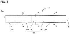
- Fig. 3 is a top view illustrating superconducting wire 2 in the superconducting wire holding structure of the first embodiment.
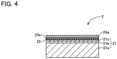
- Fig. 4 is a sectional view taken along a line IV-IV in Fig. 3 .
- Fig. 5 is a sectional view taken along a line V-V in Fig.
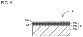
- Fig. 6 is a sectional view taken along a line VI-VI in Fig. 3 .
- a protective layer 24a and a protective layer 24b are indicated by dotted lines.
- superconducting wire 2 includes a substrate 21, an intermediate layer 22, a superconducting layer 23, protective layer 24a, and protective layer 24b.
- Substrate 21 includes a first layer 21a, a second layer 21b, and a third layer 21c.
- first layer 21a is made of stainless steel.
- Second layer 21b is formed on first layer 21a.
- second layer 21b is made of copper (Cu).
- Third layer 21c is formed on second layer 21b.
- third layer 21c is made of nickel (Ni).
- Intermediate layer 22 is formed above substrate 21 (more specifically, third layer 21c).
- Intermediate layer 22 is made of an insulating material.
- intermediate layer 22 is made of stabilized zirconia (YSZ), yttrium oxide (Y 2 O 3 ), or cerium oxide (CeO 2 ).
- the material constituting intermediate layer 22 is not limited thereto.
- Superconducting layer 23 includes a first portion 23a, a second portion 23b, and a third portion 23c along the longitudinal direction of superconducting wire 2. Third portion 23c is located between first portion 23a and second portion 23b in the longitudinal direction of superconducting wire 2.
- superconducting layer 23 is made of an oxide superconductor.
- An example of the oxide superconductor is REBaCu 3 O y (RE is a rare earth element).
- the rare earth element is yttrium (Y), praseodymium (Pr), neodymium (Nd), samarium (Sm), europium (Eu), gadolinium (Gd), holmium (Ho), or ytterbium (Yb).
- Protective layer 24a is formed on first portion 23a.
- Protective layer 24b is formed on second portion 23b.
- the protective layer is not formed on third portion 23c (the protective layer is partially removed on third portion 23c).
- protective layer 24a and protective layer 24b are electrically separated from each other.
- the protective layer is partially removed by etching.
- Fig. 7 is an exploded perspective view illustrating superconducting wire 2 and heater 4 in the superconducting wire holding structure of the first embodiment.
- heater 4 is attached to superconducting wire 2 so as to face third portion 23c.
- superconducting wire 2 is held inside holding member 1 while heater 4 is attached to superconducting wire 2.
- Heater 4 is formed of an electric heating wire such as a nichrome wire.
- Superconducting wire 2 and heater 4 constitute a persistent current switch 5.
- Fig. 8 is a schematic diagram illustrating a configuration of persistent current switch 5. As illustrated in Fig. 8 , superconducting wire 2 and a superconducting coil 6 are connected in parallel to a power source PW.
- superconducting coil 6 When heater 4 is in an off state (when the current does not flow through heater 4), superconducting coil 6 has coil impedance, so that the current flows exclusively through superconducting layer 23 in superconducting wire 2 that becomes the superconducting state. Accordingly, superconducting coil 6 is not excited (this state is referred to as a first state).
- filler 3 is filled between holding member 1 and superconducting wire 2 (and heater 4).
- Filler 3 is made of the second material.
- the second material is a material different from the first material.
- the second material is a resin material (second resin material).
- the first material is a thermosetting resin material
- the second material may be a thermoplastic resin material.
- the glass transition point of the second material (the melting point of the second material when the first material and the second material are crystalline resin materials. the same applies to the following) is less than the glass transition point of the first material.
- the viscosity of the second resin material is preferably lower than the viscosity of the first resin material. The viscosity of the first resin material and the viscosity of the second resin material are measured by a method defined in JIS Z 8803: 2011.
- a specific example of the second material is paraffin.
- the second material may be a foamed resin material.
- the second material may be a metal material.
- the melting point of the metal material is lower than the glass transition point of the first material (resin material).
- the melting point of the metal material is preferably less than or equal to 200°C.
- a specific example of the metal material is a bismuth-based alloy.
- the "bismuth-based alloy” is an alloy containing bismuth (Bi) as a main component (a component having the highest content in the alloy).
- examples of the bismuth-based alloy include a rose alloy and a Newton alloy.
- a type, component, amount, and the like of the second material are appropriately selected according to a condition required for the persistent current switch.
- superconducting wire 2 is disposed and cooled inside case 7, so that superconducting wire 2 is held at a temperature lower than or equal to the superconducting transition temperature.
- this cooling is performed by liquid nitrogen or liquid helium.
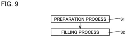
- Fig. 9 is a process diagram illustrating the method for manufacturing the superconducting wire holding structure of the first embodiment. As illustrated in Fig. 9 , the method for manufacturing the superconducting wire holding structure of the first embodiment includes a preparation process S1 and a filling process S2.
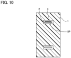
- Fig. 10 is a sectional view illustrating the superconducting wire holding structure of the first embodiment in preparation process S1. As illustrated in Fig. 10 , in preparation process S1, a void SP remains between holding member 1 and superconducting wire 2.
- filler 3 is filled between superconducting wire 2 and holding member 1 (in void SP). Filling process S2 will be specifically described with respect to the case where the first material and the second material are resin materials.
- filling process S2 firstly holding member 1 and filler 3 are heated.
- the heating temperature at this time is a temperature higher than or equal to the glass transition point of the second material and lower than the glass transition point of the first material. Filler 3 can easily flow by this heating.
- filler 3 is poured between holding member 1 and superconducting wire 2.
- Filler 3 may be filled between holding member 1 and superconducting wire 2 by immersing holding member 1 in which superconducting wire 2 is held in filler 3 heated to be in the flowing state.
- the superconducting wire holding structure is returned from the cryogenic temperature to the normal temperature.
- dew condensation is generated on the surface of the superconducting wire when the superconducting wire holding structure is returned from an extremely low temperature to the normal temperature.
- the dew condensation generated on the surface of the superconducting wire causes degradation of a superconducting characteristic of the superconducting wire.
- filler 3 is filled between holding member 1 and superconducting wire 2. That is, the surface of superconducting wire 2 is covered with filler 3. For this reason, even when the superconducting wire holding structure of the first embodiment is returned from the cryogenic temperature to the normal temperature, the dew condensation is hardly generated on the surface of superconducting wire 2.
- both the first material and the second material are resin materials and when the glass transition point of the second material is lower than the glass transition point of the first material, holding member 1 is not softened, but filler 3 is softened to be in a flowable state, so that filler 3 is easily filled between holding member 1 and superconducting wire 2. Deformation (or dissolution) of holding member 1 can be prevented when the glass transition point of the second material is lower than the glass transition point of the first material. Furthermore, in this case, when the filling of filler 3 fails, filler 3 can be removed to perform filling process S2 again, so that a yield is improved.
- This filling is more easily performed when the viscosity of the second material is relatively low (the viscosity of the second material is lower than the viscosity of the first material). In this case, the deformation of holding member 1 can be prevented when filler 3 is filled. In particular, because paraffin has a low melting point, it is easy to handle in filling process S2.
- the superconducting wire 2 can be thermally insulated, so that evaporation of the refrigerant can be prevented while the power of heater 4 can be reduced.
- the second material is a low melting point metal material such as a bismuth-based alloy
- filler 3 can function as a protective layer when quenching is generated in superconducting wire 2 due to an eddy current.
- the superconducting wire holding structure of the first embodiment even when the protective layer on third portion 23c is removed in superconducting wire 2, the degradation of the superconducting characteristic of superconducting wire 2 due to the dew condensation on the surface of superconducting wire 2 can be prevented.
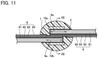
- Fig. 11 is a schematic sectional view illustrating the superconducting wire holding structure of the second embodiment.
- Fig. 12 is a sectional view taken along a line XII-XII in Fig. 11 .
- the superconducting wire holding structure of the second embodiment includes a superconducting wire 8, a superconducting wire 9, holding member 1, and filler 3.
- the superconducting wire holding structure of the second embodiment may further include a jig 10.
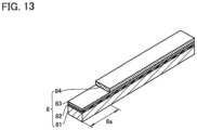
- Fig. 13 is a sectional perspective view illustrating superconducting wire 8 in the superconducting wire holding structure of the second embodiment.
- superconducting wire 8 includes a substrate 81, an intermediate layer 82, a superconducting layer 83, and a protective layer 84.
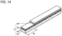
- Fig. 14 is a sectional perspective view illustrating superconducting wire 9 in the superconducting wire holding structure of the second embodiment.
- superconducting wire 9 includes a substrate 91, an intermediate layer 92, a superconducting layer 93, and a protective layer 94.
- Substrate 81 and substrate 91 have the same configuration as substrate 21.
- Intermediate layer 82 and intermediate layer 92 have the same configuration as intermediate layer 22.
- Superconducting layer 83 and superconducting layer 93 have the same configuration as superconducting layer 23.
- Protective layer 84 is formed on superconducting layer 83.
- Protective layer 94 is formed on superconducting layer 93.
- Superconducting wire 8 includes a first portion 8a at an end in the longitudinal direction of superconducting wire 8. In first portion 8a, protective layer 84 is removed. That is, in first portion 8a, superconducting layer 83 is exposed from the surface of superconducting wire 8.
- Superconducting wire 9 includes a second portion 9a at an end in the longitudinal direction of superconducting wire 9. In second portion 9a, protective layer 94 is removed. That is, in second portion 9a, superconducting layer 93 is exposed from the surface of superconducting wire 9.
- first portion 8a and second portion 9a are disposed inside holding member 1.
- Superconducting layer 83 located in first portion 8a and superconducting layer 93 located in second portion 9a are connected to each other while a connecting layer (not illustrated) made of the same oxide superconductor as superconducting layer 83 and superconducting layer 93 is interposed therebetween.
- Filler 3 is filled between holding member 1 and first portion 8a and second portion 9a.
- the material (first material) constituting holding member 1 is a resin material.
- the first material is preferably a thermosetting resin material.
- the second material is a resin material having a glass transition point lower than that of the first material.
- Jig 10 includes a first member 10a, a second member 10b, and a fixing member 10c.
- first member 10a and second member 10b are flat plate members.
- First member 10a and second member 10b are arranged to face each other with the superconducting wire 8 and the superconducting wire 9 interposed therebetween.
- Fixing member 10c is attached to first member 10a and second member 10b such that first member 10a and second member 10b sandwich superconducting wire 8 and superconducting wire 9.
- fixing member 10c includes a bolt and a nut.
- Jig 10 is disposed inside holding member 1 together with superconducting wire 8 and superconducting wire 9.
- Fig. 15 is a process diagram illustrating the method for manufacturing the superconducting wire holding structure of the second embodiment.
- the method for manufacturing the superconducting wire holding structure of the second embodiment includes preparation process S1 and filling process S2.
- the method for manufacturing the superconducting wire holding structure of the second embodiment is the same as the method for manufacturing the superconducting wire holding structure of the first embodiment.
- the method for manufacturing the superconducting wire holding structure of the second embodiment further includes a connection process S3.
- Connection process S3 is performed before preparation process S1.
- connection process S3 superconducting layer 83 located in second portion 9a and superconducting layer 93 located in second portion 9a are connected. This connection is performed using jig 10.
- first portion 8a and second portion 9b are disposed inside holding member 1 in preparation process S1. Regarding these points, the method for manufacturing the superconducting wire holding structure of the second embodiment is different from the method for manufacturing the superconducting wire holding structure of the first embodiment.
- the dew condensation may be generated on the surfaces of superconducting layer 83 and superconducting layer 93. Such dew condensation causes the degradation of the superconducting characteristics of superconducting layer 83 and superconducting layer 93.
- filler 3 is filled between first portion 8a and second portion 9a and holding member 1, so that the generation of the dew condensation as described above is prevented.
- the superconducting wire holding structure of the second embodiment includes jig 10 disposed inside holding member 1, connection strength between superconducting wire 8 and superconducting wire 9 can be increased.
- jig 10 has no need to be removed after connection process S3 is completed, so that the manufacturing process can be simplified. Furthermore, in this case, a decrease in yield due to the occurrence of an operation error during the removal of jig 10 can be prevented.
Landscapes
- Superconductors And Manufacturing Methods Therefor (AREA)
- Containers, Films, And Cooling For Superconductive Devices (AREA)
Claims (16)
- Haltestruktur für supraleitenden Draht, umfassend:ein Halteelement (1), das aus einem ersten Material hergestellt ist;einen supraleitenden Draht (2), der im Inneren des Halteelements (1) angeordnet ist; undeinen Füllstoff (3), der aus einem zweiten, vom ersten Material verschiedenen Material besteht,wobei der supraleitende Draht (2) umfasst:ein Substrat (21);eine Zwischenschicht (22), die auf dem Substrat (21) ausgebildet ist;eine supraleitende Schicht (23), die auf der Zwischenschicht (22) ausgebildet ist; und gekennzeichnet ist durcheine erste Schutzschicht (24a) und eine zweite Schutzschicht (24b), ausgebildet auf der supraleitenden Schicht (23), und dassdie supraleitende Schicht (23) einen ersten Abschnitt (23a), einen zweiten Abschnitt (23b) und einen dritten Abschnitt (23c) zwischen dem ersten Abschnitt (23a) und dem zweiten Abschnitt (23b) entlang einer Längsrichtung des supraleitenden Drahtes (2) aufweist, und dassdie erste Schutzschicht (24a) auf dem ersten Abschnitt (23a) ausgebildet ist, und dassdie zweite Schutzschicht (24b) auf dem zweiten Abschnitt (23b) ausgebildet ist, und dassder Füllstoff (3) zwischen dem dritten Abschnitt (23c) und dem Halteelement (1) eingefüllt wird.
- Haltestruktur für supraleitenden Draht nach Anspruch 1, wobei das erste Material ein erstes Harzmaterial ist, und das zweite Material ein zweites Harzmaterial ist.
- Haltestruktur für supraleitenden Draht nach Anspruch 2, wobei der Glasübergangspunkt des zweiten Harzmaterials niedriger ist als der Glasübergangspunkt des ersten Harzmaterials.
- Haltestruktur für supraleitenden Draht nach Anspruch 2, wobei die Viskosität des zweiten Harzmaterials niedriger ist als die Viskosität des ersten Harzmaterials.
- Haltestruktur für supraleitenden Draht nach einem der Ansprüche 2 bis 4, wobei das erste Harzmaterial ein wärmehärtendes Harz ist, und das zweite Harzmaterial ein thermoplastisches Harz ist.
- Haltestruktur für supraleitenden Draht nach einem der Ansprüche 2 bis 5, wobei das zweite Harzmaterial Paraffin ist.
- Haltestruktur für supraleitenden Draht nach einem der Ansprüche 1 bis 6, wobei die supraleitende Drahthaltestruktur einen Dauerstromschalter darstellt.
- Haltestruktur für supraleitenden Draht nach Anspruch 1, wobei das erste Material ein Harzmaterial ist, das zweite Material ein Metallmaterial ist, und ein Schmelzpunkt des Metallmaterials niedriger ist als ein Glasübergangspunkt des Harzmaterials.
- Haltestruktur für supraleitenden Draht nach Anspruch 8, wobei das Harzmaterial ein duroplastisches Harz ist.
- Haltestruktur für supraleitenden Draht nach Anspruch 8 oder 9, wobei der Schmelzpunkt des Metallmaterials weniger als oder gleich 200°C beträgt.
- Haltestruktur für supraleitenden Draht nach einem der Ansprüche 8 bis 10, wobei das Metallmaterial eine Legierung auf Wismutbasis ist.
- Eine Haltestruktur für supraleitenden Draht, umfassend:einen ersten supraleitenden Draht (8), der eine erste supraleitende Schicht (83) enthält;einen zweiten supraleitenden Draht (9), der eine zweite supraleitende Schicht (93) enthält;ein Halteelement (1) aus einem ersten Material; undeinen Füllstoff (3) aus einem zweiten Material, das sich von dem ersten Material unterscheidet,wobei der erste supraleitende Draht (8) einen ersten Abschnitt (8a) aufweist, in dem die erste supraleitende Schicht (83) von einer Oberfläche des ersten supraleitenden Drahtes (8) an einem Ende in einer Längsrichtung des ersten supraleitenden Drahtes (8) freigelegt ist,der zweite supraleitende Draht (9) einen zweiten Abschnitt (9a) aufweist, wo die zweite supraleitende Schicht (93) von einer Oberfläche des zweiten supraleitenden Drahtes (9) an einem Ende in einer Längsrichtung des zweiten supraleitenden Drahtes (9) freiliegt,der erste Abschnitt (8a) und der zweite Abschnitt (9a) innerhalb des Halteelements (1) angeordnet sind,die erste supraleitende Schicht (83), die sich in dem ersten Abschnitt (8a) befindet, und die zweite supraleitende Schicht (93), die sich in dem zweiten Abschnitt (9a) befindet, miteinander verbunden sind, undder Füllstoff (3) zwischen dem Halteelement (1) und dem ersten Abschnitt (8a) und dem zweiten Abschnitt (9a) eingefüllt ist, dadurch gekennzeichnet, dassdas erste Material ein erstes Harzmaterial ist, und dassdas zweite Material ein zweites Harzmaterial ist.
- Haltestruktur für supraleitenden Draht nach Anspruch 12, wobei der Glasübergangspunkt des zweiten Harzmaterials niedriger ist als der Glasübergangspunkt des ersten Harzmaterials.
- Haltestruktur für supraleitenden Draht nach Anspruch 12, wobei die Viskosität des zweiten Harzmaterials niedriger ist als die Viskosität des ersten Harzmaterials.
- Haltestruktur für supraleitenden Draht nach Anspruch 12, wobei das erste Harzmaterial ein wärmehärtendes Harz ist, und das zweite Harzmaterial ein thermoplastisches Harz ist.
- Haltestruktur für supraleitenden Draht nach einem der Ansprüche 12 bis 15, wobei das zweite Harzmaterial Paraffin ist.
Applications Claiming Priority (2)
| Application Number | Priority Date | Filing Date | Title |
|---|---|---|---|
| JP2019171839 | 2019-09-20 | ||
| PCT/JP2020/032809 WO2021054093A1 (ja) | 2019-09-20 | 2020-08-31 | 超電導線材保持構造 |
Publications (3)
| Publication Number | Publication Date |
|---|---|
| EP4033552A1 EP4033552A1 (de) | 2022-07-27 |
| EP4033552A4 EP4033552A4 (de) | 2023-05-03 |
| EP4033552B1 true EP4033552B1 (de) | 2024-06-12 |
Family
ID=74883452
Family Applications (1)
| Application Number | Title | Priority Date | Filing Date |
|---|---|---|---|
| EP20866135.5A Active EP4033552B1 (de) | 2019-09-20 | 2020-08-31 | Struktur zum halten eines supraleitenden drahtes |
Country Status (4)
| Country | Link |
|---|---|
| US (1) | US20220351880A1 (de) |
| EP (1) | EP4033552B1 (de) |
| JP (1) | JP7515492B2 (de) |
| WO (1) | WO2021054093A1 (de) |
Family Cites Families (15)
| Publication number | Priority date | Publication date | Assignee | Title |
|---|---|---|---|---|
| JPS5112790A (en) * | 1974-07-03 | 1976-01-31 | Furukawa Electric Co Ltd | Chodendosenno setsuzokubu oyobi sonosetsuzokuhoho |
| JP4058920B2 (ja) * | 2001-07-10 | 2008-03-12 | 株式会社日立製作所 | 超電導接続構造 |
| JP4593933B2 (ja) * | 2004-01-22 | 2010-12-08 | 住友電気工業株式会社 | 多相超電導ケーブルの接続構造 |
| US7816303B2 (en) * | 2004-10-01 | 2010-10-19 | American Superconductor Corporation | Architecture for high temperature superconductor wire |
| WO2006095602A1 (ja) * | 2005-03-07 | 2006-09-14 | Matsushita Electric Industrial Co., Ltd. | 実装体及びその製造方法 |
| JP2011165435A (ja) * | 2010-02-08 | 2011-08-25 | Sumitomo Electric Ind Ltd | 超電導線材の接続構造体 |
| JP2016106378A (ja) * | 2016-03-11 | 2016-06-16 | 住友電気工業株式会社 | 超電導線及びその製造方法 |
| JP6734092B2 (ja) * | 2016-03-29 | 2020-08-05 | 古河電気工業株式会社 | 超電導線材の接続構造 |
| CN109923624B (zh) * | 2016-10-31 | 2020-09-08 | 住友电气工业株式会社 | 超导线材和超导线圈 |
| JP6998667B2 (ja) | 2017-03-30 | 2022-01-18 | 古河電気工業株式会社 | 接続構造体 |
| WO2018211699A1 (ja) * | 2017-05-19 | 2018-11-22 | 住友電気工業株式会社 | 超電導線材、超電導コイル、超電導マグネット及び超電導機器 |
| JP6513134B2 (ja) * | 2017-05-26 | 2019-05-15 | レノボ・シンガポール・プライベート・リミテッド | ケーブル接続構造及びケーブル接続方法 |
| US20200343652A1 (en) * | 2017-11-28 | 2020-10-29 | Basf Se | Joined superconducting tape |
| JP6862382B2 (ja) * | 2018-03-07 | 2021-04-21 | 株式会社東芝 | 高温超電導磁石装置、その運転制御装置及び方法 |
| JP7200609B2 (ja) | 2018-03-28 | 2023-01-10 | 大日本印刷株式会社 | 熱転写シート |
-
2020
- 2020-08-31 WO PCT/JP2020/032809 patent/WO2021054093A1/ja not_active Ceased
- 2020-08-31 JP JP2021546579A patent/JP7515492B2/ja active Active
- 2020-08-31 EP EP20866135.5A patent/EP4033552B1/de active Active
- 2020-08-31 US US17/760,781 patent/US20220351880A1/en not_active Abandoned
Also Published As
| Publication number | Publication date |
|---|---|
| WO2021054093A1 (ja) | 2021-03-25 |
| JP7515492B2 (ja) | 2024-07-12 |
| JPWO2021054093A1 (de) | 2021-03-25 |
| EP4033552A1 (de) | 2022-07-27 |
| EP4033552A4 (de) | 2023-05-03 |
| US20220351880A1 (en) | 2022-11-03 |
Similar Documents
| Publication | Publication Date | Title |
|---|---|---|
| KR101374177B1 (ko) | 고온 초전도체층의 직접 접촉에 의한 부분 미세 용융 확산 압접을 이용한 2세대 ReBCO 고온 초전도체의 접합 및 산소 공급 어닐링 열처리에 의한 초전도 회복 방법 | |
| US20150357089A1 (en) | METHOD OF PERSISTENT CURRENT MODE SPLICING OF 2G ReBCO HIGH TEMPERATURE SUPERCONDUCTORS USING SOLID STATE PRESSURIZED ATOMS DIFFUSION BY DIRECT FACE-TO-FACE CONTACT OF HIGH TEMPERATURE SUPERCONDUCTING LAYERS AND RECOVERING SUPERCONDUCTIVITY BY OXYGENATION ANNEALING | |
| JP6998667B2 (ja) | 接続構造体 | |
| JP6505565B2 (ja) | 高温超電導導体、高温超電導コイル及び高温超電導コイルの接続構造 | |
| JP5118990B2 (ja) | 超電導テープ線材及び欠陥部の補修方法 | |
| EP4033552B1 (de) | Struktur zum halten eines supraleitenden drahtes | |
| JP6086852B2 (ja) | 酸化物超電導線材、酸化物超電導線材の接続構造体、酸化物超電導線材と電極端子の接続構造体、及びこれを備えた超電導機器、並びにこれらの製造方法 | |
| JP2009230913A (ja) | 酸化物超電導電流リード | |
| JP7279723B2 (ja) | 超電導線材及び永久電流スイッチ | |
| US11980106B2 (en) | Persistent current switch and superconducting device | |
| JP5789696B1 (ja) | 超電導電流リード及び超電導電流リードの製造方法 | |
| JP6353334B2 (ja) | 超電導電流リード | |
| JP2005100683A (ja) | 酸化物超電導体通電素子 | |
| JP6314022B2 (ja) | 超電導電流リード及び超電導電流リードの製造方法 | |
| JP6238623B2 (ja) | 超電導電流リード | |
| KR20240164912A (ko) | 밀폐된 고온 초전도 테이프 도체 | |
| JP2018055990A (ja) | 超電導電流リード及び酸化物超電導線材 | |
| EP4033551A1 (de) | Dauerstromschalter und supraleitende vorrichtung | |
| Makida et al. | Development of an ASTROMAG test coil with aluminum stabilized superconductor | |
| JP2004047259A (ja) | 酸化物超電導体通電素子 | |
| Schoerling et al. | Electrical resistance of Nb3Sn/Cu splices produced by electromagnetic pulse technology and soft soldering | |
| JP2008177245A (ja) | 酸化物超電導体通電素子及びその製造方法 | |
| JP4012422B2 (ja) | 酸化物超電導体電流リード | |
| JP2007115635A (ja) | 高温超電導コイル及びその製造方法 | |
| JP2021166126A (ja) | 超電導電流リード |
Legal Events
| Date | Code | Title | Description |
|---|---|---|---|
| STAA | Information on the status of an ep patent application or granted ep patent |
Free format text: STATUS: THE INTERNATIONAL PUBLICATION HAS BEEN MADE |
|
| PUAI | Public reference made under article 153(3) epc to a published international application that has entered the european phase |
Free format text: ORIGINAL CODE: 0009012 |
|
| STAA | Information on the status of an ep patent application or granted ep patent |
Free format text: STATUS: REQUEST FOR EXAMINATION WAS MADE |
|
| 17P | Request for examination filed |
Effective date: 20220317 |
|
| AK | Designated contracting states |
Kind code of ref document: A1 Designated state(s): AL AT BE BG CH CY CZ DE DK EE ES FI FR GB GR HR HU IE IS IT LI LT LU LV MC MK MT NL NO PL PT RO RS SE SI SK SM TR |
|
| DAV | Request for validation of the european patent (deleted) | ||
| DAX | Request for extension of the european patent (deleted) | ||
| REG | Reference to a national code |
Ref country code: DE Ref country code: DE Ref legal event code: R079 Ref document number: 602020032462 Country of ref document: DE Free format text: PREVIOUS MAIN CLASS: H01L0039160000 Ipc: H10N0060810000 |
|
| A4 | Supplementary search report drawn up and despatched |
Effective date: 20230403 |
|
| RIC1 | Information provided on ipc code assigned before grant |
Ipc: H01B 12/06 20060101ALI20230328BHEP Ipc: H10N 60/81 20230101AFI20230328BHEP |
|
| REG | Reference to a national code |
Ref country code: DE Ref legal event code: R079 Free format text: PREVIOUS MAIN CLASS: H10N0060810000 Ipc: H01B0012060000 Ref country code: DE Ref legal event code: R079 Ref document number: 602020032462 Country of ref document: DE Free format text: PREVIOUS MAIN CLASS: H10N0060810000 Ipc: H01B0012060000 |
|
| RIC1 | Information provided on ipc code assigned before grant |
Ipc: H10N 60/81 20230101ALI20231109BHEP Ipc: H01B 12/06 20060101AFI20231109BHEP |
|
| GRAP | Despatch of communication of intention to grant a patent |
Free format text: ORIGINAL CODE: EPIDOSNIGR1 |
|
| STAA | Information on the status of an ep patent application or granted ep patent |
Free format text: STATUS: GRANT OF PATENT IS INTENDED |
|
| INTG | Intention to grant announced |
Effective date: 20240115 |
|
| GRAS | Grant fee paid |
Free format text: ORIGINAL CODE: EPIDOSNIGR3 |
|
| GRAA | (expected) grant |
Free format text: ORIGINAL CODE: 0009210 |
|
| STAA | Information on the status of an ep patent application or granted ep patent |
Free format text: STATUS: THE PATENT HAS BEEN GRANTED |
|
| P01 | Opt-out of the competence of the unified patent court (upc) registered |
Effective date: 20240404 |
|
| AK | Designated contracting states |
Kind code of ref document: B1 Designated state(s): AL AT BE BG CH CY CZ DE DK EE ES FI FR GB GR HR HU IE IS IT LI LT LU LV MC MK MT NL NO PL PT RO RS SE SI SK SM TR |
|
| REG | Reference to a national code |
Ref country code: GB Ref legal event code: FG4D |
|
| REG | Reference to a national code |
Ref country code: CH Ref legal event code: EP |
|
| REG | Reference to a national code |
Ref country code: DE Ref legal event code: R096 Ref document number: 602020032462 Country of ref document: DE |
|
| REG | Reference to a national code |
Ref country code: IE Ref legal event code: FG4D |
|
| REG | Reference to a national code |
Ref country code: CH Ref legal event code: PK Free format text: BERICHTIGUNGEN |
|
| PG25 | Lapsed in a contracting state [announced via postgrant information from national office to epo] |
Ref country code: BG Free format text: LAPSE BECAUSE OF FAILURE TO SUBMIT A TRANSLATION OF THE DESCRIPTION OR TO PAY THE FEE WITHIN THE PRESCRIBED TIME-LIMIT Effective date: 20240612 |
|
| PG25 | Lapsed in a contracting state [announced via postgrant information from national office to epo] |
Ref country code: HR Free format text: LAPSE BECAUSE OF FAILURE TO SUBMIT A TRANSLATION OF THE DESCRIPTION OR TO PAY THE FEE WITHIN THE PRESCRIBED TIME-LIMIT Effective date: 20240612 Ref country code: FI Free format text: LAPSE BECAUSE OF FAILURE TO SUBMIT A TRANSLATION OF THE DESCRIPTION OR TO PAY THE FEE WITHIN THE PRESCRIBED TIME-LIMIT Effective date: 20240612 |
|
| REG | Reference to a national code |
Ref country code: LT Ref legal event code: MG9D |
|
| PG25 | Lapsed in a contracting state [announced via postgrant information from national office to epo] |
Ref country code: GR Free format text: LAPSE BECAUSE OF FAILURE TO SUBMIT A TRANSLATION OF THE DESCRIPTION OR TO PAY THE FEE WITHIN THE PRESCRIBED TIME-LIMIT Effective date: 20240913 |
|
| REG | Reference to a national code |
Ref country code: NL Ref legal event code: MP Effective date: 20240612 |
|
| PG25 | Lapsed in a contracting state [announced via postgrant information from national office to epo] |
Ref country code: ES Free format text: LAPSE BECAUSE OF FAILURE TO SUBMIT A TRANSLATION OF THE DESCRIPTION OR TO PAY THE FEE WITHIN THE PRESCRIBED TIME-LIMIT Effective date: 20240612 |
|
| PG25 | Lapsed in a contracting state [announced via postgrant information from national office to epo] |
Ref country code: LV Free format text: LAPSE BECAUSE OF FAILURE TO SUBMIT A TRANSLATION OF THE DESCRIPTION OR TO PAY THE FEE WITHIN THE PRESCRIBED TIME-LIMIT Effective date: 20240612 |
|
| PG25 | Lapsed in a contracting state [announced via postgrant information from national office to epo] |
Ref country code: NO Free format text: LAPSE BECAUSE OF FAILURE TO SUBMIT A TRANSLATION OF THE DESCRIPTION OR TO PAY THE FEE WITHIN THE PRESCRIBED TIME-LIMIT Effective date: 20240912 Ref country code: LV Free format text: LAPSE BECAUSE OF FAILURE TO SUBMIT A TRANSLATION OF THE DESCRIPTION OR TO PAY THE FEE WITHIN THE PRESCRIBED TIME-LIMIT Effective date: 20240612 Ref country code: HR Free format text: LAPSE BECAUSE OF FAILURE TO SUBMIT A TRANSLATION OF THE DESCRIPTION OR TO PAY THE FEE WITHIN THE PRESCRIBED TIME-LIMIT Effective date: 20240612 Ref country code: GR Free format text: LAPSE BECAUSE OF FAILURE TO SUBMIT A TRANSLATION OF THE DESCRIPTION OR TO PAY THE FEE WITHIN THE PRESCRIBED TIME-LIMIT Effective date: 20240913 Ref country code: FI Free format text: LAPSE BECAUSE OF FAILURE TO SUBMIT A TRANSLATION OF THE DESCRIPTION OR TO PAY THE FEE WITHIN THE PRESCRIBED TIME-LIMIT Effective date: 20240612 Ref country code: ES Free format text: LAPSE BECAUSE OF FAILURE TO SUBMIT A TRANSLATION OF THE DESCRIPTION OR TO PAY THE FEE WITHIN THE PRESCRIBED TIME-LIMIT Effective date: 20240612 Ref country code: BG Free format text: LAPSE BECAUSE OF FAILURE TO SUBMIT A TRANSLATION OF THE DESCRIPTION OR TO PAY THE FEE WITHIN THE PRESCRIBED TIME-LIMIT Effective date: 20240612 Ref country code: RS Free format text: LAPSE BECAUSE OF FAILURE TO SUBMIT A TRANSLATION OF THE DESCRIPTION OR TO PAY THE FEE WITHIN THE PRESCRIBED TIME-LIMIT Effective date: 20240912 |
|
| PG25 | Lapsed in a contracting state [announced via postgrant information from national office to epo] |
Ref country code: NL Free format text: LAPSE BECAUSE OF FAILURE TO SUBMIT A TRANSLATION OF THE DESCRIPTION OR TO PAY THE FEE WITHIN THE PRESCRIBED TIME-LIMIT Effective date: 20240612 |
|
| REG | Reference to a national code |
Ref country code: AT Ref legal event code: MK05 Ref document number: 1694931 Country of ref document: AT Kind code of ref document: T Effective date: 20240612 |
|
| PG25 | Lapsed in a contracting state [announced via postgrant information from national office to epo] |
Ref country code: NL Free format text: LAPSE BECAUSE OF FAILURE TO SUBMIT A TRANSLATION OF THE DESCRIPTION OR TO PAY THE FEE WITHIN THE PRESCRIBED TIME-LIMIT Effective date: 20240612 |
|
| PG25 | Lapsed in a contracting state [announced via postgrant information from national office to epo] |
Ref country code: PT Free format text: LAPSE BECAUSE OF FAILURE TO SUBMIT A TRANSLATION OF THE DESCRIPTION OR TO PAY THE FEE WITHIN THE PRESCRIBED TIME-LIMIT Effective date: 20241014 |
|
| PG25 | Lapsed in a contracting state [announced via postgrant information from national office to epo] |
Ref country code: PT Free format text: LAPSE BECAUSE OF FAILURE TO SUBMIT A TRANSLATION OF THE DESCRIPTION OR TO PAY THE FEE WITHIN THE PRESCRIBED TIME-LIMIT Effective date: 20241014 |
|
| PG25 | Lapsed in a contracting state [announced via postgrant information from national office to epo] |
Ref country code: PL Free format text: LAPSE BECAUSE OF FAILURE TO SUBMIT A TRANSLATION OF THE DESCRIPTION OR TO PAY THE FEE WITHIN THE PRESCRIBED TIME-LIMIT Effective date: 20240612 |
|
| PG25 | Lapsed in a contracting state [announced via postgrant information from national office to epo] |
Ref country code: EE Free format text: LAPSE BECAUSE OF FAILURE TO SUBMIT A TRANSLATION OF THE DESCRIPTION OR TO PAY THE FEE WITHIN THE PRESCRIBED TIME-LIMIT Effective date: 20240612 |
|
| PG25 | Lapsed in a contracting state [announced via postgrant information from national office to epo] |
Ref country code: AT Free format text: LAPSE BECAUSE OF FAILURE TO SUBMIT A TRANSLATION OF THE DESCRIPTION OR TO PAY THE FEE WITHIN THE PRESCRIBED TIME-LIMIT Effective date: 20240612 Ref country code: IS Free format text: LAPSE BECAUSE OF FAILURE TO SUBMIT A TRANSLATION OF THE DESCRIPTION OR TO PAY THE FEE WITHIN THE PRESCRIBED TIME-LIMIT Effective date: 20241012 |
|
| PG25 | Lapsed in a contracting state [announced via postgrant information from national office to epo] |
Ref country code: CZ Free format text: LAPSE BECAUSE OF FAILURE TO SUBMIT A TRANSLATION OF THE DESCRIPTION OR TO PAY THE FEE WITHIN THE PRESCRIBED TIME-LIMIT Effective date: 20240612 |
|
| PG25 | Lapsed in a contracting state [announced via postgrant information from national office to epo] |
Ref country code: SK Free format text: LAPSE BECAUSE OF FAILURE TO SUBMIT A TRANSLATION OF THE DESCRIPTION OR TO PAY THE FEE WITHIN THE PRESCRIBED TIME-LIMIT Effective date: 20240612 Ref country code: RO Free format text: LAPSE BECAUSE OF FAILURE TO SUBMIT A TRANSLATION OF THE DESCRIPTION OR TO PAY THE FEE WITHIN THE PRESCRIBED TIME-LIMIT Effective date: 20240612 |
|
| PG25 | Lapsed in a contracting state [announced via postgrant information from national office to epo] |
Ref country code: SM Free format text: LAPSE BECAUSE OF FAILURE TO SUBMIT A TRANSLATION OF THE DESCRIPTION OR TO PAY THE FEE WITHIN THE PRESCRIBED TIME-LIMIT Effective date: 20240612 |
|
| PG25 | Lapsed in a contracting state [announced via postgrant information from national office to epo] |
Ref country code: SM Free format text: LAPSE BECAUSE OF FAILURE TO SUBMIT A TRANSLATION OF THE DESCRIPTION OR TO PAY THE FEE WITHIN THE PRESCRIBED TIME-LIMIT Effective date: 20240612 Ref country code: SK Free format text: LAPSE BECAUSE OF FAILURE TO SUBMIT A TRANSLATION OF THE DESCRIPTION OR TO PAY THE FEE WITHIN THE PRESCRIBED TIME-LIMIT Effective date: 20240612 Ref country code: RO Free format text: LAPSE BECAUSE OF FAILURE TO SUBMIT A TRANSLATION OF THE DESCRIPTION OR TO PAY THE FEE WITHIN THE PRESCRIBED TIME-LIMIT Effective date: 20240612 Ref country code: PL Free format text: LAPSE BECAUSE OF FAILURE TO SUBMIT A TRANSLATION OF THE DESCRIPTION OR TO PAY THE FEE WITHIN THE PRESCRIBED TIME-LIMIT Effective date: 20240612 Ref country code: IS Free format text: LAPSE BECAUSE OF FAILURE TO SUBMIT A TRANSLATION OF THE DESCRIPTION OR TO PAY THE FEE WITHIN THE PRESCRIBED TIME-LIMIT Effective date: 20241012 Ref country code: EE Free format text: LAPSE BECAUSE OF FAILURE TO SUBMIT A TRANSLATION OF THE DESCRIPTION OR TO PAY THE FEE WITHIN THE PRESCRIBED TIME-LIMIT Effective date: 20240612 Ref country code: CZ Free format text: LAPSE BECAUSE OF FAILURE TO SUBMIT A TRANSLATION OF THE DESCRIPTION OR TO PAY THE FEE WITHIN THE PRESCRIBED TIME-LIMIT Effective date: 20240612 Ref country code: AT Free format text: LAPSE BECAUSE OF FAILURE TO SUBMIT A TRANSLATION OF THE DESCRIPTION OR TO PAY THE FEE WITHIN THE PRESCRIBED TIME-LIMIT Effective date: 20240612 |
|
| PG25 | Lapsed in a contracting state [announced via postgrant information from national office to epo] |
Ref country code: IT Free format text: LAPSE BECAUSE OF FAILURE TO SUBMIT A TRANSLATION OF THE DESCRIPTION OR TO PAY THE FEE WITHIN THE PRESCRIBED TIME-LIMIT Effective date: 20240612 |
|
| REG | Reference to a national code |
Ref country code: DE Ref legal event code: R119 Ref document number: 602020032462 Country of ref document: DE |
|
| PG25 | Lapsed in a contracting state [announced via postgrant information from national office to epo] |
Ref country code: DK Free format text: LAPSE BECAUSE OF FAILURE TO SUBMIT A TRANSLATION OF THE DESCRIPTION OR TO PAY THE FEE WITHIN THE PRESCRIBED TIME-LIMIT Effective date: 20240612 |
|
| PG25 | Lapsed in a contracting state [announced via postgrant information from national office to epo] |
Ref country code: LU Free format text: LAPSE BECAUSE OF NON-PAYMENT OF DUE FEES Effective date: 20240831 |
|
| PLBE | No opposition filed within time limit |
Free format text: ORIGINAL CODE: 0009261 |
|
| STAA | Information on the status of an ep patent application or granted ep patent |
Free format text: STATUS: NO OPPOSITION FILED WITHIN TIME LIMIT |
|
| PG25 | Lapsed in a contracting state [announced via postgrant information from national office to epo] |
Ref country code: MC Free format text: LAPSE BECAUSE OF FAILURE TO SUBMIT A TRANSLATION OF THE DESCRIPTION OR TO PAY THE FEE WITHIN THE PRESCRIBED TIME-LIMIT Effective date: 20240612 |
|
| 26N | No opposition filed |
Effective date: 20250313 |
|
| GBPC | Gb: european patent ceased through non-payment of renewal fee |
Effective date: 20240912 |
|
| REG | Reference to a national code |
Ref country code: BE Ref legal event code: MM Effective date: 20240831 |
|
| PG25 | Lapsed in a contracting state [announced via postgrant information from national office to epo] |
Ref country code: DE Free format text: LAPSE BECAUSE OF NON-PAYMENT OF DUE FEES Effective date: 20250301 |
|
| PG25 | Lapsed in a contracting state [announced via postgrant information from national office to epo] |
Ref country code: GB Free format text: LAPSE BECAUSE OF NON-PAYMENT OF DUE FEES Effective date: 20240912 |
|
| PG25 | Lapsed in a contracting state [announced via postgrant information from national office to epo] |
Ref country code: BE Free format text: LAPSE BECAUSE OF NON-PAYMENT OF DUE FEES Effective date: 20240831 |
|
| PG25 | Lapsed in a contracting state [announced via postgrant information from national office to epo] |
Ref country code: FR Free format text: LAPSE BECAUSE OF NON-PAYMENT OF DUE FEES Effective date: 20240831 |
|
| PG25 | Lapsed in a contracting state [announced via postgrant information from national office to epo] |
Ref country code: IE Free format text: LAPSE BECAUSE OF NON-PAYMENT OF DUE FEES Effective date: 20240831 |
|
| PG25 | Lapsed in a contracting state [announced via postgrant information from national office to epo] |
Ref country code: SE Free format text: LAPSE BECAUSE OF FAILURE TO SUBMIT A TRANSLATION OF THE DESCRIPTION OR TO PAY THE FEE WITHIN THE PRESCRIBED TIME-LIMIT Effective date: 20240612 |
|
| PGFP | Annual fee paid to national office [announced via postgrant information from national office to epo] |
Ref country code: CH Payment date: 20250901 Year of fee payment: 6 |
|
| PG25 | Lapsed in a contracting state [announced via postgrant information from national office to epo] |
Ref country code: CY Free format text: LAPSE BECAUSE OF FAILURE TO SUBMIT A TRANSLATION OF THE DESCRIPTION OR TO PAY THE FEE WITHIN THE PRESCRIBED TIME-LIMIT; INVALID AB INITIO Effective date: 20200831 |
|
| PG25 | Lapsed in a contracting state [announced via postgrant information from national office to epo] |
Ref country code: HU Free format text: LAPSE BECAUSE OF FAILURE TO SUBMIT A TRANSLATION OF THE DESCRIPTION OR TO PAY THE FEE WITHIN THE PRESCRIBED TIME-LIMIT; INVALID AB INITIO Effective date: 20200831 |