EP4024397B1 - Taktschaltung und speicher - Google Patents
Taktschaltung und speicher Download PDFInfo
- Publication number
- EP4024397B1 EP4024397B1 EP21868221.9A EP21868221A EP4024397B1 EP 4024397 B1 EP4024397 B1 EP 4024397B1 EP 21868221 A EP21868221 A EP 21868221A EP 4024397 B1 EP4024397 B1 EP 4024397B1
- Authority
- EP
- European Patent Office
- Prior art keywords
- data strobe
- clock
- circuit
- signal
- transmission circuit
- Prior art date
- Legal status (The legal status is an assumption and is not a legal conclusion. Google has not performed a legal analysis and makes no representation as to the accuracy of the status listed.)
- Active
Links
Images

Classifications
-
- G—PHYSICS
- G11—INFORMATION STORAGE
- G11C—STATIC STORES
- G11C11/00—Digital stores characterised by the use of particular electric or magnetic storage elements; Storage elements therefor
- G11C11/21—Digital stores characterised by the use of particular electric or magnetic storage elements; Storage elements therefor using electric elements
- G11C11/34—Digital stores characterised by the use of particular electric or magnetic storage elements; Storage elements therefor using electric elements using semiconductor devices
- G11C11/40—Digital stores characterised by the use of particular electric or magnetic storage elements; Storage elements therefor using electric elements using semiconductor devices using transistors
- G11C11/401—Digital stores characterised by the use of particular electric or magnetic storage elements; Storage elements therefor using electric elements using semiconductor devices using transistors forming cells needing refreshing or charge regeneration, i.e. dynamic cells
- G11C11/406—Management or control of the refreshing or charge-regeneration cycles
-
- G—PHYSICS
- G11—INFORMATION STORAGE
- G11C—STATIC STORES
- G11C7/00—Arrangements for writing information into, or reading information out from, a digital store
- G11C7/22—Read-write [R-W] timing or clocking circuits; Read-write [R-W] control signal generators or management
- G11C7/222—Clock generating, synchronizing or distributing circuits within memory device
-
- H—ELECTRICITY
- H03—ELECTRONIC CIRCUITRY
- H03K—PULSE TECHNIQUE
- H03K19/00—Logic circuits, i.e. having at least two inputs acting on one output; Inverting circuits
- H03K19/02—Logic circuits, i.e. having at least two inputs acting on one output; Inverting circuits using specified components
- H03K19/08—Logic circuits, i.e. having at least two inputs acting on one output; Inverting circuits using specified components using semiconductor devices
- H03K19/094—Logic circuits, i.e. having at least two inputs acting on one output; Inverting circuits using specified components using semiconductor devices using field-effect transistors
- H03K19/09432—Logic circuits, i.e. having at least two inputs acting on one output; Inverting circuits using specified components using semiconductor devices using field-effect transistors with coupled sources or source coupled logic
-
- G—PHYSICS
- G11—INFORMATION STORAGE
- G11C—STATIC STORES
- G11C11/00—Digital stores characterised by the use of particular electric or magnetic storage elements; Storage elements therefor
- G11C11/21—Digital stores characterised by the use of particular electric or magnetic storage elements; Storage elements therefor using electric elements
- G11C11/34—Digital stores characterised by the use of particular electric or magnetic storage elements; Storage elements therefor using electric elements using semiconductor devices
- G11C11/40—Digital stores characterised by the use of particular electric or magnetic storage elements; Storage elements therefor using electric elements using semiconductor devices using transistors
- G11C11/401—Digital stores characterised by the use of particular electric or magnetic storage elements; Storage elements therefor using electric elements using semiconductor devices using transistors forming cells needing refreshing or charge regeneration, i.e. dynamic cells
- G11C11/4063—Auxiliary circuits, e.g. for addressing, decoding, driving, writing, sensing or timing
- G11C11/407—Auxiliary circuits, e.g. for addressing, decoding, driving, writing, sensing or timing for memory cells of the field-effect type
- G11C11/4076—Timing circuits
-
- G—PHYSICS
- G11—INFORMATION STORAGE
- G11C—STATIC STORES
- G11C7/00—Arrangements for writing information into, or reading information out from, a digital store
- G11C7/10—Input/output [I/O] data interface arrangements, e.g. I/O data control circuits, I/O data buffers
- G11C7/1078—Data input circuits, e.g. write amplifiers, data input buffers, data input registers, data input level conversion circuits
- G11C7/1093—Input synchronization
Definitions
- Embodiments of the present disclosure relate to the field of semiconductor technologies, and in particular to a clock circuit and a memory.
- the Dynamic Random Access Memory is a semiconductor memory device commonly used in computers, and is composed of many repeated memory cells. Each memory cell generally includes a capacitor and a transistor. The gate of the transistor is connected to a word line, the drain of the transistor is connected to a bit line, and the source of the transistor is connected to the capacitor. A voltage signal on the word line can control turn-on or turn-off of the transistor, such that data information stored in the capacitor can be read through the bit line or data information can be written into the capacitor through the bit line for storage.
- the DRAM may include the Double Data Rate (DDR) synchronous DRAM, the Graphics Double Data Rate (GDDR) DRAM, and the Low Power Double Data Rate (LPDDR) synchronous DRAM.
- DDR Double Data Rate
- GDDR Graphics Double Data Rate
- LPDDR Low Power Double Data Rate
- US2018247683A1 relates to an apparatus for determining a phase relationship between an input clock signal and a multiphase clock signal.
- the apparatus includes a clock path configured to receive a clock signal and provide internal clock signals and a command path configured to receive a command and propagate the command through the command path responsive to the internal clock signals and provide an internal command having a timing that reflects a timing of the clock signal.
- the apparatus further includes a data clock path and a clock synchronization circuit.
- the technical problem solved by embodiments of the present disclosure is to provide a clock circuit and a memory, so as to solve the problem that a system clock signal does not match a data strobe clock signal.
- the invention is set out in the appended set of claims.
- the system clock module includes at least two first signal transmission paths, and transmits the system clock signal via different first signal transmission paths among the at least two first signal transmission paths based on at least one of: different receiving rates, or different sending rates of the data signal.
- the data strobe clock signal is transmitted at different transmission rates, correspondingly, the system clock signal is transmitted via the different first signal transmission paths, so that the data strobe clock signal transmitted at the different transmission rates can all be matched with the system clock signal correspondingly. Therefore, although the transmission rate of the data strobe clock signal may change, the clock difference between the data strobe clock signal and the system clock signal changes little, or the clock difference between the data strobe clock signal and the system clock signal can even remain unchanged. Therefore, the handshake module can well align the data strobe clock signal and the system clock signal, thereby making synchronization and handshake functions easier to implement.
- a WCK clock signal i.e., a data strobe clock signal
- a data transmission rate of the same memory may be fast or slow, and accordingly, a transmission rate of the WCK clock signal may exceed a preset value or may be lower than the preset value. For example, if the data transmission rate exceeds 3200 Mbps, a Current Mode Logic (CML) frequency divider can be introduced to reduce interference on the WCK clock signal; if the data transmission rate is lower than 3200 Mbps, a CMOS frequency divider can be used to save power consumption to the greatest extent.
- CML Current Mode Logic
- the WCK clock signal is transmitted via different transmission paths.
- a CK clock signal i.e., a system clock signal
- the alignment of a clock domain of the WCK clock signal and a clock domain of the CK clock signal needs to be considered, and the WCK2CK synchronization and handshake functions between the two clock domains should also be considered. If the CK clock signal is transmitted via the same transmission path, it is difficult to ensure that the CK clock signal has excellent synchronization performance with both the high-speed WCK clock signal and the low-speed WCK clock signal.
- the embodiments of the present disclosure provide a clock circuit, so as to ensure that the CK clock signal has excellent synchronization performance with both the high-speed and low-speed WCK clock signals.
- FIG. 1 illustrates a functional block diagram of a clock circuit, which is not part of the present invention and is present for illustration purpose.
- FIG. 2 illustrates another functional block diagram of a clock circuit, which is not part of the present invention and is present for illustration purpose.
- FIG. 3 illustrates a diagram of the working principle of a data strobe clock module in FIG. 2 .
- FIG. 4 illustrates yet another functional block diagram of a clock circuit.
- FIG. 5 illustrates a structural diagram of a clock circuit provided by an embodiment of the present disclosure.
- FIG. 6 illustrates another structural diagram of a clock circuit provided by an embodiment of the present disclosure.
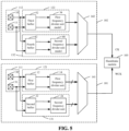
- the clock circuit includes: a data strobe clock module 101 and a system clock module 102.
- the data strobe clock module 101 is configured to receive a data strobe clock signal WCK and transmit the data strobe clock signal WCK, herein, the data strobe clock signal WCK is used for controlling at least one of receiving or sending of a data signal.
- the system clock module 102 is configured to receive a system clock signal CK and transmit the system clock signal CK, herein, the system clock signal CK is used for controlling receiving of a command signal.
- the system clock module 102 includes at least two first signal transmission paths, and is configured to transmit the system clock signal CK via different first signal transmission paths among the at least two first signal transmission paths based on at least one of: different receiving rates, or different sending rates of the data signal.
- the at least one of: the receiving rates, or the sending rates of the data signals may include a high transmission rate and a low transmission rate, and correspondingly, the data strobe clock signal WCK has a high-speed signal transmission path and a low-speed signal transmission path.
- the data strobe clock module 101 has different second signal transmission paths, including the low-speed signal transmission path and the high-speed signal transmission path, so that when the data strobe clock signal WCK is a high-speed clock signal, the corresponding signal transmission path has a strong anti-interference capability, and when the data strobe clock signal WCK is a low-speed clock signal, the corresponding signal transmission path has low power consumption, thereby satisfying the requirement for the strong anti-interference capability in the case of the high-speed clock signal and the requirement for low power consumption in the case of the low-speed clock signal.
- the high speed and the low speed are two relative expressions and thus are clearly defined.
- the system clock module 102 has different first signal transmission paths, and each first signal transmission path corresponds to a respective signal transmission path in the data strobe clock module 101, so that each first signal transmission path matches the respective one of the second signal transmission paths.
- the matching can be understood as: the influence of each first signal transmission path on the system clock signal CK and the influence of the second signal transmission path corresponding to the first signal transmission path on the data strobe clock signal WCK are synchronous.
- the influence includes clock signal delay, clock signal loss, clock signal disturbance, and/or the like.
- the matching of the clock signal delay is performed between each first signal transmission path and the second signal transmission path corresponding to the first signal transmission path, so that the data strobe clock signal WCK having different transmission rates can well implement synchronous handshake with the system clock signal CK.
- the clock circuit further includes a handshake module 103 connected to the data strobe clock module 101 and the system clock module 102, and configured to determine a phase relationship between the system clock signal CK and the data strobe clock signal WCK.
- the data strobe clock module 101 includes at least two second signal transmission paths, the data strobe clock signal WCK is transmitted via different second signal transmission paths among the at least two second signal transmission paths at different transmission rates, each of the transmission rates corresponds to a respective one of the at least one of: the receiving rates, or the sending rates, and each of the second signal transmission paths corresponds to a respective one of the first signal transmission paths.
- the system clock module 102 is configured to transmit, when the data strobe clock signal WCK is transmitted via a second signal transmission path in the second signal transmission paths, the system clock signal CK via the first signal transmission path corresponding to the second signal transmission path. That is to say, when the data strobe clock module 101 uses a specific second signal transmission path to transmit the data strobe clock signal WCK, the system clock module 102 also uses a specific corresponding first signal transmission path to transmit the system clock signal CK.
- the data strobe clock module 101 includes a first data strobe clock transmission circuit 121 and a second data strobe clock transmission circuit 131.
- the first data strobe clock transmission circuit 121 and the second data strobe clock transmission circuit 131 define the different second signal transmission paths.
- the data strobe clock module 101 is configured to transmit, if a transmission rate in the transmission rates is greater than or equal to a preset value, the data strobe clock signal WCK through the first data strobe clock transmission circuit 121; and transmit, if the transmission rate is less than the preset value, the data strobe clock signal WCK through the second data strobe clock transmission circuit 131.
- the preset value can be reasonably set according to performance requirements of a memory; the first data strobe clock transmission circuit 121 is configured to define the high-speed transmission path; and the second data strobe clock transmission circuit 131 is configured to define the low-speed transmission path.
- the data strobe clock module may also include three or more second signal transmission paths, that is, the data strobe clock module has three or more data strobe clock transmission circuits.
- the data strobe clock module 101 further includes: a first selector circuit 141 and a data clock pad 111.
- the first selector circuit 141 is configured to select an output signal of one of the first data strobe clock transmission circuit 121 and the second data strobe clock transmission circuit 131 for output.
- the data clock pad 111 is configured to receive the data strobe clock signal WCK and transmit the data strobe clock signal WCK to the first data strobe clock transmission circuit 121 and the second data strobe clock transmission circuit 131.
- the data strobe clock signal WCK is transmitted to the first data strobe clock transmission circuit 121 and the second data strobe clock transmission circuit 131 through the data clock pad 111, and after transmission via two second signal transmission paths, two data strobe clock signals WCK reach the first selector circuit 141; and the first selector circuit 141 selects, based on a receiving rate or a sending rate of the data signal among the at least one of: the receiving rates, or the sending rates of the data signal, the output signal of the first data strobe clock transmission circuit 121 or the second data strobe clock transmission circuit 131 for output.
- the first selector circuit 141 selects the output signal of the second data strobe clock transmission circuit 131 for output; if the receiving rate or the sending rate of the data signal is greater than or equal to the preset value, the first selector circuit 141 selects the output signal of the first data strobe clock transmission circuit 121 for output.
- the data strobe clock signal WCK is transmitted to the first data strobe clock transmission circuit 121 and the second data strobe clock transmission circuit 131 through the data clock pad 111; and the first selector circuit 141 selects one of the first data strobe clock transmission circuit 121 and the second data strobe clock transmission circuit 131 for clock signal transmission, and the other of the first data strobe clock transmission circuit 121 and the second data strobe clock transmission circuit 131 does not operate. In this case, only one of the first data strobe clock transmission circuit 121 and the second data strobe clock transmission circuit 131 operates, so that the power consumption of the clock circuit can be further reduced.
- the data strobe clock signal WCK output by the first selector circuit 141 can be used for implement "read”, “write”, “handshake” and other functions.
- the data strobe clock signal WCK is transmitted to multiple corresponding data receivers.
- the output of the data strobe clock module 101 is provided by the second data strobe clock transmission circuit 131, in order to avoid the problems such as transmission loss caused by the first selector circuit 141 to the data strobe clock signal WCK, the output of the second data strobe clock transmission circuit 131 can also be directly output to the handshake module 103 to implement the "handshake" function, without passing through the first selector circuit 141.
- the system clock module 102 includes a system clock pad 112 and a system clock transmission circuit 152.
- the system clock pad 112 is configured to receive the system clock signal CK and transmit the system clock signal to the system clock transmission circuit 152, and the system clock transmission circuit 152 has the at least two first signal transmission paths.
- the system clock module 102 includes a first system clock transmission circuit 122 and a second system clock transmission circuit 132.
- the first system clock transmission circuit 122 and the second system clock transmission circuit 132 define the different first signal transmission paths.
- the system clock module 102 is configured to transmit, if the data strobe clock signal WCK is transmitted through the first data strobe clock transmission circuit 121, the system clock signal CK through the first system clock transmission circuit 122, and transmit, if the data strobe clock signal WCK is transmitted through the second data strobe clock transmission circuit 131, the system clock signal CK through the second system clock transmission circuit 132.
- the first system clock transmission circuit 122 is configured to match the first data strobe clock transmission circuit 121
- the second system clock transmission circuit 132 is configured to match the second data strobe clock transmission circuit 131.
- a clock delay of the first system clock transmission circuit 122 with respect to the system clock signal CK matches a clock delay of the first data strobe clock transmission circuit 121 with respect to the data strobe clock signal WCK
- a clock delay of the second system clock transmission circuit 132 with respect to the system clock signal CK matches a clock delay of the second data strobe clock transmission circuit 131 with respect to the data strobe clock signal WCK.
- the data strobe clock module has three or more second signal transmission paths
- the system clock module also has three or more first signal transmission paths, that is, the system clock module also has three or more system clock transmission circuits.
- the system clock module further includes a second selector circuit 142.
- the second selector circuit 142 is configured to select an output signal of one of the first system clock transmission circuit 122 and the second system clock transmission circuit 132 for output.
- the system clock signal CK is transmitted to the first system clock transmission circuit 122 and the second system clock transmission circuit 132 through the system clock pad 112, and after transmission via two first signal transmission paths, two system clock signals CK reach the second selector circuit 142; and the second selector circuit 142 selects, based on the receiving rate or the sending rate of the data signal, the output signal of the first system clock transmission circuit 122 or the second system clock transmission circuit 132 for output.
- the second selector circuit 142 selects the output signal of the second system clock transmission circuit 132 for output; if the receiving rate or the sending rate of the data signal is greater than or equal to the preset value, the second selector circuit 142 selects the output signal of the first system clock transmission circuit 122 for output.
- the data system signal CK is transmitted to the first system clock transmission circuit 122 and the second system clock transmission circuit 132 through the system clock pad 112; and the second selector circuit 142 selects one of the first system clock transmission circuit 122 and the second system clock transmission circuit 132 for clock signal transmission, and the other of the first system clock transmission circuit 122 and the second system clock transmission circuit 132 does not operate. In this case, only one of the first system clock transmission circuit 122 and the second system clock transmission circuit 132 operates, so that the power consumption of the clock circuit can be further reduced.
- the system clock module 102 Since the system clock module 102 has multiple first signal transmission paths, better clock matching can be achieved for the data strobe clock signal WCK having different transmission rates. For example, the system clock signal CK and the data strobe clock signal WCK match in clock delay, clock jitter and/or the like. Therefore, even if the receiving rate or the sending rate of the data signal changes, the handshake module 103 can still implement synchronous handshake between the system clock signal CK and the data strobe clock signal WCK.
- the handshake module 103 is connected to outputs of the first selector circuit 141 and the second selector circuit 142 and configured to determine a phase relationship between the system clock signal and the data strobe clock signal.
- the data strobe clock signal WCK may be a differential clock signal.
- the data clock pad 111 includes a first data clock pad 30 and a second data clock pad 31 configured to respectively receive the differential data strobe clock signals WCK, which can be called as a WCK_t clock signal and a WCK_c clock signal.
- the system clock signal CK may be a differential clock signal.
- the system clock pad 112 includes a first system clock pad 10 and a second system clock pad 11 configured to respectively receive the differential system clock signals CK, which may be a CK_t clock signal and a CK_c clock signal.
- the first data strobe clock transmission circuit 121 includes a first frequency divider unit 14; the second data strobe clock transmission circuit 131 includes a second frequency divider unit 24; and the first frequency divider unit 14 is configured to divide a frequency of the data strobe clock signal WCK and output at least two frequency-divided data strobe clock signals having different phases, and the second frequency divider unit 24 is configured to divide a frequency of the data strobe clock signal WCK and output at least two frequency-divided data strobe clock signals having different phases.
- the first frequency divider unit 14 has a first correlation between power consumption and the frequency of the data strobe clock signal WCK
- the second frequency divider unit 24 has a second correlation between power consumption and the frequency of the data strobe clock signal WCK, and the first correlation is weaker than the second correlation; and/or, the first frequency divider unit 14 has a first anti-interference capability, the second frequency divider unit 24 has a second anti-interference capability, and the first anti-interference capability is stronger than the second anti-interference capability.
- the first frequency divider unit 14 is configured to divide the frequency of the data strobe clock signal WCK having a high transmission rate
- the second frequency divider unit 24 is configured to divide the frequency of the data strobe clock signal WCK having a low transmission rate. That is, the first frequency divider unit 14 divides the frequency of the data strobe clock signal WCK having the high frequency
- the second frequency divider unit 24 divides the frequency of the data strobe clock signal WCK having the low frequency. Since the first correlation is weaker than the second correlation and a static power consumption of the first frequency divider unit 14 is higher than a static power consumption of the second frequency divider unit 24, the second frequency divider unit 24 can maintain relatively low power consumption, thereby avoiding the problem of excessive power consumption of a low-speed transmission path.
- the first anti-interference capability is stronger than the second anti-interference capability, the problem that a high-speed transmission path causes interference on the data strobe clock signal WCK is avoided, so that the data strobe clock signal WCK transmitted via the high-speed transmission path has high accuracy.
- the first frequency divider unit 14 includes a current-mode logic (CML) frequency divider circuit, and in FIG. 6 , the CML frequency divider circuit is denoted as CML DIV; and the second frequency divider unit 24 includes a Complementary Metal Oxide Semiconductor (CMOS) frequency divider circuit, and in FIG. 6 , the CMOS frequency divider circuit is denoted as CMOS DIV.
- CML current-mode logic
- CMOS Complementary Metal Oxide Semiconductor
- the static power consumption is relatively high, the correlation between the power consumption and the frequency is weak, the anti-interference capability is strong, and the anti-interference capability for power supply jitter/toggle is strong; and for the CMOS frequency divider circuit, the power consumption is low, the correlation between the power consumption and the frequency is strong, the lower the frequency, the lower the power consumption, the influence of power supply noise on clock jitter is large, and the capability of resisting against power supply interference is weak.
- the high-speed transmission path uses the CML frequency divider circuit to ensure the strong anti-interference capability of the data strobe clock signal, and the low-speed transmission path uses the CMOS frequency divider circuit with the low power consumption to achieve the objective of power saving in the case of a low speed.
- the first data strobe clock transmission circuit 121 further includes a CML to CMOS unit, configured to be connected to the CML frequency divider circuit and output the frequency-divided data strobe clock signals.
- the CML to CMOS unit is defined as a first CML to CMOS unit 15. As illustrated in FIG. 6 , in FIG. 6 , the first CML to CMOS unit 15 is denoted as C2C1.
- the second data strobe clock transmission circuit 131 further includes a CML to CMOS unit 25, configured to output the data strobe clock signal to the CMOS frequency divider circuit.
- the CML to CMOS unit is defined as a second CML to CMOS unit 25. As illustrated in FIG. 6 , in FIG. 6 , the second CML to CMOS unit 25 is denoted as C2C2.
- each of the first data strobe clock transmission circuit 121 and the second data strobe clock transmission circuit 131 includes a buffer, configured to buffer and receive the data strobe clock signal.
- the buffer in the first data strobe clock transmission circuit 121 is defined as a first buffer 12
- the buffer in the second data strobe clock transmission circuit 131 is defined as a second buffer 22.
- the buffer is a CML buffer.
- the first buffer 12 is denoted as CML bufferl
- the second buffer 22 is denoted as CML buffer2.
- the first system clock transmission circuit 122 includes a first frequency divider unit model 34
- the second system clock transmission circuit 132 includes a second frequency divider unit model 44
- the first frequency divider unit model 34 is configured to match a clock delay of the first data strobe clock transmission circuit 121
- the second frequency divider unit model 44 is configured to match a clock delay of the second data strobe clock transmission circuit 131.
- first frequency divider unit model 34 does not actually perform frequency division processing on the system clock signal
- second frequency divider unit model 44 does not actually perform frequency division processing on the system clock signal
- the first frequency divider unit model 34 includes a CML frequency divider circuit model
- the second frequency divider unit model 44 includes a CMOS frequency divider circuit model.
- the CML frequency divider circuit model is denoted as CML DIV Model
- the CMOS frequency divider circuit model is denoted as CMOS DIV Model.
- the first system clock transmission circuit 122 further includes a CML to CMOS unit, configured to be connected to the CML frequency divider circuit model and output the system clock signal.
- the CML to CMOS unit is defined as a third CML to CMOS unit 35.
- the third CML to CMOS unit 35 is denoted as C2C3.
- the second system clock transmission circuit 132 further includes a CML to CMOS unit, configured to output the system clock signal to the CMOS frequency divider circuit model.
- the CML to CMOS unit is defined as a fourth CML to CMOS unit 45.
- the fourth CML to CMOS unit 45 is denoted as C2C4.
- Each of the first system clock transmission circuit 122 and the second system clock transmission circuit 132 includes a buffer, configured to buffer and receive the system clock signal.
- the buffer in the first system clock transmission circuit 122 is defined as a third buffer 32
- the buffer in the second system clock transmission circuit 132 is defined as a fourth buffer 42.
- the buffer is a CML buffer.
- the third buffer 32 is denoted as CML buffer3
- the fourth buffer 42 is denoted as CML buffer4.
- the buffer is the CML buffer.
- the above buffer may also be a CMOS buffer, and accordingly, there is no need to provide the CML to CMOS unit between the buffer and another structure (such as the CMOS frequency divider unit).
- first data strobe clock transmission circuit 121, the second data strobe clock transmission circuit 131, the first system clock transmission circuit 122, and the second system clock transmission circuit 132 each include a Duty Cycle Adjuster (DCA) unit, configured to adjust a duty cycle of the data strobe clock signal or a duty cycle of the system clock signal.
- the DCA unit in the first data strobe clock transmission circuit 121 is defined as a first DCA unit 13
- the DCA unit in the second data strobe clock transmission circuit 131 is defined as a second DCA unit 23
- the DCA unit in the first system clock transmission circuit 122 is defined as a third DCA unit 33
- the DCA unit in the second system clock transmission circuit 132 is defined as a fourth DCA unit 43.
- the first DCA unit 13, the second DCA unit 23, the third DCA unit 33, and the fourth DCA unit 43 are respectively denoted as DCA1, DCA2, DCA3, and DCA4.
- the system clock module 102 includes at least two first signal transmission paths, and transmits the system clock signal via different paths among the at least two first signal transmission paths based on at least one of: different receiving rates, or different sending rates of the data signal.
- the data strobe clock signal is transmitted at different transmission rates, correspondingly, the system clock signal is transmitted via the different first signal transmission paths, so that the data strobe clock signal transmitted at the different transmission rates can all be matched with the system clock signal accordingly. Therefore, although the transmission rate of the data strobe clock signal changes, the clock difference between the data strobe clock signal and the system clock signal changes little, or the clock difference between the data strobe clock signal and the system clock signal can even remain unchanged. Therefore, the handshake module 103 can well align the data strobe clock signal and the system clock signal, thereby making synchronization and handshake functions easier to implement.
- the first data strobe clock transmission circuit 121 that defines the high-speed transmission path includes the CML frequency divider circuit, and the CML frequency divider circuit has the advantage of the strong anti-interference capability, so that there is little interference on the data strobe clock signal transmitted at a high speed, thereby ensuring the accuracy of the data strobe clock signal.
- the second data strobe clock transmission circuit 131 that defines the low-speed transmission path includes the CMOS frequency divider circuit, and the CMOS frequency divider circuit has the advantage of the low power consumption, thereby facilitating reducing power consumption of the clock circuit. Therefore, this embodiment has the advantages of the strong anti-interference capability in the case of the high speed and the low power consumption in the case of the low speed.
- the embodiments of the present disclosure further provide a memory, including the aforementioned clock circuit.
- the memory may be a DDR memory, such as a DDR5 memory.
- the system clock module includes at least two first signal transmission paths, and transmits the system clock signal via different paths among the at least two first signal transmission paths based on at least one of: different receiving rates, or different sending rates of the data signal.
- the data strobe clock signal is transmitted at different transmission rates, correspondingly, the system clock signal is transmitted via the different first signal transmission paths, so that the data strobe clock signal transmitted at the different transmission rates can be matched with the system clock signal accordingly. Therefore, although the transmission rate of the data strobe clock signal changes, the clock difference between the data strobe clock signal and the system clock signal changes little, or the clock difference between the data strobe clock signal and the system clock signal can even remain unchanged. Therefore, the handshake module can well align the data strobe clock signal and the system clock signal, thereby making synchronization and handshake functions easier to implement.
Landscapes
- Engineering & Computer Science (AREA)
- Computer Hardware Design (AREA)
- Microelectronics & Electronic Packaging (AREA)
- Mathematical Physics (AREA)
- Computing Systems (AREA)
- General Engineering & Computer Science (AREA)
- Physics & Mathematics (AREA)
- Power Engineering (AREA)
- Dram (AREA)
- Dc Digital Transmission (AREA)
- Memory System (AREA)
- Synchronisation In Digital Transmission Systems (AREA)
- Logic Circuits (AREA)
Claims (14)
- Taktschaltung, umfassend:ein Daten-Strobe-Taktmodul (101), das so konfiguriert ist, dass es ein Daten-Strobe-Taktsignal empfängt und das Daten-Strobe-Taktsignal sendet, wobei das Daten-Strobe-Taktsignal dazu verwendet wird, den Empfang und/oder das Senden von mindestens einem Datensignal zu steuern; undein Systemtaktmodul (102), das so konfiguriert ist, dass es ein Systemtaktsignal empfängt und das Systemtaktsignal sendet, wobei das Systemtaktsignal dazu verwendet wird, den Empfang eines Befehlssignals zu steuern;dadurch gekennzeichnet, dass das Systemtaktmodul (102) mindestens zwei erste Signalübertragungspfade umfasst und so konfiguriert ist, dass es das Systemtaktsignal über unterschiedliche erste Signalübertragungspfade der mindestens zwei ersten Signalübertragungspfade auf der Grundlage von mindestens einen der folgenden Raten überträgt: unterschiedliche Empfangsraten oder Senderaten des Datensignals;das Daten-Strobe-Taktmodul (101) mindestens zwei zweite Signalübertragungspfade umfasst, das Daten-Strobe-Taktsignal über unterschiedliche zweite Signalübertragungspfade der mindestens zwei zweiten Signalübertragungspfade mit unterschiedlichen Übertragungsraten übertragen wird, jede der Übertragungsraten einer jeweiligen der mindestens einen der folgenden Raten entspricht: den Empfangsraten oder den Senderaten, und jeder der zweiten Signalübertragungspfade an einen jeweiligen der ersten Signalübertragungspfade angepasst ist; und wobei das Systemtaktmodul (102) so konfiguriert ist, dass es, wenn das Daten-Strobe-Taktsignal über einen zweiten Signalübertragungspfad unter den zweiten Signalübertragungspfaden übertragen wird, das Systemtaktsignal über den ersten Signalübertragungspfad überträgt, der an den zweiten Signalübertragungspfad angepasst ist,wobei das Daten-Strobe-Taktmodul (101) ferner eine erste Daten-Strobe-Taktübertragungsschaltung (121) und eine zweite Daten-Strobe-Taktübertragungsschaltung (131) umfasst, und die erste Daten-Strobe-Taktübertragungsschaltung (121) und die zweite Daten-Strobe-Taktübertragungsschaltung (131) die unterschiedlichen zweiten Signalübertragungspfade definieren;wobei das Systemtaktmodul (102) ferner eine erste Systemtaktübertragungsschaltung (122) und eine zweite Systemtaktübertragungsschaltung (132) umfasst, und die erste Systemtaktübertragungsschaltung (122) und die zweite Systemtaktübertragungsschaltung (132) die unterschiedlichen ersten Signalübertragungspfade definieren, undwobei die erste Systemtaktübertragungsschaltung (122) so konfiguriert ist, dass sie mit der ersten Daten-Strobe-Taktübertragungsschaltung (121) übereinstimmt, und die zweite Systemtaktübertragungsschaltung (132) so konfiguriert ist, dass sie mit der zweiten Daten-Strobe-Taktübertragungsschaltung (131) übereinstimmt.
- Taktschaltung nach Anspruch 1, wobei das Daten-Strobe-Taktmodul (101) so konfiguriert ist, dass es, wenn eine Übertragungsrate in den Übertragungsraten größer oder gleich einem voreingestellten Wert ist, das Daten-Strobe-Taktsignal über die erste Daten-Strobe-Taktübertragungsschaltung (121) überträgt und, wenn die Übertragungsrate kleiner als der voreingestellte Wert ist, das Daten-Strobe-Taktsignal über die zweite Daten-Strobe-Taktübertragungsschaltung (131) überträgt.
- Taktschaltung nach Anspruch 2, wobei die erste Daten-Strobe-Taktübertragungsschaltung (121) eine erste Frequenzteilereinheit (14) umfasst; die zweite Daten-Strobe-Taktübertragungsschaltung (131) eine zweite Frequenzteilereinheit (24) umfasst; und die erste Frequenzteilereinheit (14) so konfiguriert ist, dass sie eine Frequenz des Daten-Strobe-Taktsignals teilt und mindestens zwei frequenzgeteilte Daten-Strobe-Taktsignale mit unterschiedlichen Phasen ausgibt, und die zweite Frequenzteilereinheit (24) so konfiguriert ist, dass sie eine Frequenz des Daten-Strobe-Taktsignals teilt und mindestens zwei frequenzgeteilte Daten-Strobe-Taktsignale mit unterschiedlichen Phasen ausgibt.
- Taktschaltung nach Anspruch 3, wobei die erste Frequenzteilereinheit (14) eine erste Korrelation zwischen dem Stromverbrauch und der Frequenz des Daten-Strobe-Taktsignals aufweist, die zweite Frequenzteilereinheit (24) eine zweite Korrelation zwischen dem Stromverbrauch und der Frequenz des Daten-Strobe-Taktsignals aufweist, und die erste Korrelation schwächer ist als die zweite Korrelation; oder die erste Frequenzteilereinheit (14) eine erste Anti-Interferenz-Fähigkeit besitzt, die zweite Frequenzteilereinheit (24) eine zweite Anti-Interferenz-Fähigkeit besitzt und die erste Anti-Interferenz-Fähigkeit stärker als die zweite Anti-Interferenz-Fähigkeit ist.
- Taktschaltung nach Anspruch 3 oder 4, wobei die erste Frequenzteilereinheit (14) eine Frequenzteilerschaltung mit Stromschaltlogik umfasst und die zweite Frequenzteilereinheit (24) eine Frequenzteilerschaltung mit komplementären Metalloxidhalbleitern (CMOS) umfasst.
- Taktschaltung nach Anspruch 5, wobei die erste Daten-Strobe-Taktübertragungsschaltung (121) ferner eine Stromschaltlogik-CMOS-Einheit umfasst, die so konfiguriert ist, dass sie mit der Frequenzteilerschaltung mit Stromschaltlogik verbunden wird und die frequenzgeteilten Daten-Strobe-Taktsignale ausgibt.
- Taktschaltung nach Anspruch 5, wobei die zweite Daten-Strobe-Taktübertragungsschaltung (131) ferner eine Stromschaltlogik-CMOS-Einheit umfasst, die so konfiguriert ist, dass sie das Daten-Strobe-Taktsignal an die CMOS-Frequenzteilerschaltung ausgibt.
- Taktschaltung nach Anspruch 2, wobei sowohl die erste Daten-Strobe-Taktübertragungsschaltung (121) als auch die zweite Daten-Strobe-Taktübertragungsschaltung (131) einen Puffer umfasst, der zum Puffern und Empfangen des Daten-Strobe-Taktsignals konfiguriert ist, und
wobei der Puffer ein Logikpuffer mit Stromschaltlogik ist. - Taktschaltung nach Anspruch 2, wobei das Systemtaktmodul (102) so konfiguriert ist, dass es, wenn das Daten-Strobe-Taktsignal über die erste Daten-Strobe-Taktübertragungsschaltung (121) übertragen wird, das Systemtaktsignal über die erste Systemtaktübertragungsschaltung (122) überträgt, und, wenn das Daten-Strobe-Taktsignal über die zweite Daten-Strobe-Taktübertragungsschaltung (131) übertragen wird, das Systemtaktsignal über die zweite Systemtaktübertragungsschaltung (132) überträgt.
- Taktschaltung nach Anspruch 9, wobei die erste Systemtaktübertragungsschaltung (122) ein erstes Frequenzteilereinheitsmodell (34) umfasst und die zweite Systemtaktübertragungsschaltung (132) ein zweites Frequenzteilereinheitsmodell (44) umfasst; und das erste Frequenzteilereinheitsmodell (34) so konfiguriert ist, dass es an eine Taktverzögerung der ersten Daten-Strobe-Taktübertragungsschaltung (121) angepasst ist, und das zweite Frequenzteilereinheitsmodell (44) so konfiguriert ist, dass es an eine Taktverzögerung der zweiten Daten-Strobe-Taktübertragungsschaltung (131) angepasst ist; und
wobei das erste Frequenzteilereinheitsmodell (34) ein Frequenzteilerschaltungsmodell mit Stromschaltlogik umfasst und das zweite Frequenzteilereinheitsmodell (44) ein Frequenzteilerschaltungsmodell mit komplementären Metalloxidhalbleitern (CMOS) umfasst. - Taktschaltung nach Anspruch 10, wobei die erste Systemtaktübertragungsschaltung (122) ferner eine Stromschaltlogik-CMOS-Einheit umfasst, die so konfiguriert ist, dass sie mit dem Frequenzteilerschaltungsmodell mit Stromschaltlogik verbunden wird und das Systemtaktsignal ausgibt;wobei die zweite Systemtaktübertragungsschaltung (132) ferner eine Stromschaltlogik-CMOS-Einheit umfasst, die so konfiguriert ist, dass sie das Systemtaktsignal an das CMOS-Frequenzteilerschaltungsmodell ausgibt;wobei sowohl die erste Systemtaktübertragungsschaltung (122) als auch die zweite Systemtaktübertragungsschaltung (132) einen Puffer umfasst, der zum Puffern und Empfangen des Daten-Strobe-Taktsignals konfiguriert ist, und wobei der Puffer ein Logikpuffer mit Stromschaltlogik ist.
- Taktschaltung nach Anspruch 9, wobei das Daten-Strobe-Taktmodul (101) ferner eine erste Selektorschaltung (141) umfasst, und die erste Selektorschaltung (141) so konfiguriert ist, dass sie ein Ausgangssignal der ersten Daten-Strobe-Taktübertragungsschaltung (121) oder der zweiten Daten-Strobe-Taktübertragungsschaltung (131) zur Ausgabe auswählt; und das Systemtaktmodul (102) ferner eine zweite Selektorschaltung (142) umfasst, und die zweite Selektorschaltung (142) so konfiguriert ist, dass sie ein Ausgangssignal der ersten Systemtaktübertragungsschaltung (122) oder der zweiten Systemtaktübertragungsschaltung (132) zur Ausgabe auswählt.
- Taktschaltung nach Anspruch 12, ferner umfassend ein Handshake-Modul (103), das mit Ausgängen der ersten Selektorschaltung (141) und der zweiten Selektorschaltung (142) verbunden ist und so konfiguriert ist, dass es eine Phasenbeziehung zwischen dem Systemtaktsignal und dem Daten-Strobe-Taktsignal bestimmt.
- Speicher, umfassend:
die Taktschaltung nach einem der Ansprüche 1 bis 13.
Applications Claiming Priority (2)
| Application Number | Priority Date | Filing Date | Title |
|---|---|---|---|
| CN202010969644.7A CN114187942B (zh) | 2020-09-15 | 2020-09-15 | 时钟电路以及存储器 |
| PCT/CN2021/104551 WO2022057392A1 (zh) | 2020-09-15 | 2021-07-05 | 时钟电路以及存储器 |
Publications (3)
| Publication Number | Publication Date |
|---|---|
| EP4024397A1 EP4024397A1 (de) | 2022-07-06 |
| EP4024397A4 EP4024397A4 (de) | 2022-12-21 |
| EP4024397B1 true EP4024397B1 (de) | 2024-11-06 |
Family
ID=80539769
Family Applications (1)
| Application Number | Title | Priority Date | Filing Date |
|---|---|---|---|
| EP21868221.9A Active EP4024397B1 (de) | 2020-09-15 | 2021-07-05 | Taktschaltung und speicher |
Country Status (6)
| Country | Link |
|---|---|
| US (1) | US12033684B2 (de) |
| EP (1) | EP4024397B1 (de) |
| JP (1) | JP7316460B2 (de) |
| KR (1) | KR102710353B1 (de) |
| CN (1) | CN114187942B (de) |
| WO (1) | WO2022057392A1 (de) |
Families Citing this family (1)
| Publication number | Priority date | Publication date | Assignee | Title |
|---|---|---|---|---|
| TWI900008B (zh) * | 2024-05-16 | 2025-10-01 | 晶豪科技股份有限公司 | 訊號恢復系統以及儲存裝置 |
Family Cites Families (19)
| Publication number | Priority date | Publication date | Assignee | Title |
|---|---|---|---|---|
| US6897697B2 (en) * | 1999-06-28 | 2005-05-24 | Broadcom Corporation | Current-controlled CMOS circuit using higher voltage supply in low voltage CMOS process |
| JP4828203B2 (ja) * | 2005-10-20 | 2011-11-30 | エルピーダメモリ株式会社 | 同期型半導体記憶装置 |
| KR100903370B1 (ko) * | 2007-11-02 | 2009-06-23 | 주식회사 하이닉스반도체 | 데이터 클록 트레이닝 회로, 그를 포함한 반도체 메모리 장치 및 시스템 |
| KR100910852B1 (ko) * | 2007-12-26 | 2009-08-06 | 주식회사 하이닉스반도체 | 반도체 메모리 소자 |
| KR101499176B1 (ko) | 2008-04-08 | 2015-03-06 | 삼성전자주식회사 | 클럭 신호의 위상 튜닝 방법 및 그 장치 |
| KR100929828B1 (ko) * | 2008-09-02 | 2009-12-07 | 주식회사 하이닉스반도체 | 반도체 메모리 장치 |
| JP5624441B2 (ja) * | 2010-11-30 | 2014-11-12 | ピーエスフォー ルクスコ エスエイアールエルPS4 Luxco S.a.r.l. | 半導体装置 |
| KR20120076814A (ko) * | 2010-12-30 | 2012-07-10 | 에스케이하이닉스 주식회사 | 집적회로 칩, 마스터 칩과 슬레이브 칩을 포함하는 시스템 및 이의 동작방법 |
| KR102272259B1 (ko) * | 2015-07-01 | 2021-07-06 | 삼성전자주식회사 | 커맨드 연동 클럭 생성 스키마를 갖는 반도체 메모리 장치 |
| US20170243628A1 (en) * | 2016-02-22 | 2017-08-24 | Mediatek Inc. | Termination topology of memory system and associated memory module and control method |
| US10186309B2 (en) * | 2016-06-29 | 2019-01-22 | Samsung Electronics Co., Ltd. | Methods of operating semiconductor memory devices and semiconductor memory devices |
| KR102641515B1 (ko) | 2016-09-19 | 2024-02-28 | 삼성전자주식회사 | 메모리 장치 및 그것의 클록 분배 방법 |
| KR102623542B1 (ko) * | 2016-10-07 | 2024-01-10 | 삼성전자주식회사 | 멀티플 클럭 도메인 메모리 장치의 클럭 동기화 방법 |
| US10210918B2 (en) * | 2017-02-28 | 2019-02-19 | Micron Technology, Inc. | Apparatuses and methods for determining a phase relationship between an input clock signal and a multiphase clock signal |
| KR102530884B1 (ko) | 2018-04-06 | 2023-05-11 | 에스케이하이닉스 주식회사 | 반도체 메모리 장치 및 반도체 메모리 장치의 동작 방법 |
| US10593383B1 (en) * | 2018-09-04 | 2020-03-17 | Micron Technology, Inc. | System-level timing budget improvements |
| US10762947B2 (en) * | 2018-10-04 | 2020-09-01 | Samsung Electronics Co., Ltd. | Memory devices |
| CN212484941U (zh) * | 2020-09-15 | 2021-02-05 | 长鑫存储技术有限公司 | 时钟电路以及存储器 |
| CN116805867A (zh) * | 2022-03-23 | 2023-09-26 | 三星电子株式会社 | 存储器件、存储器件和存储器控制器的操作方法 |
-
2020
- 2020-09-15 CN CN202010969644.7A patent/CN114187942B/zh active Active
-
2021
- 2021-07-05 EP EP21868221.9A patent/EP4024397B1/de active Active
- 2021-07-05 KR KR1020227021268A patent/KR102710353B1/ko active Active
- 2021-07-05 WO PCT/CN2021/104551 patent/WO2022057392A1/zh not_active Ceased
- 2021-07-05 JP JP2022538825A patent/JP7316460B2/ja active Active
-
2022
- 2022-03-31 US US17/709,708 patent/US12033684B2/en active Active
Also Published As
| Publication number | Publication date |
|---|---|
| JP2023508059A (ja) | 2023-02-28 |
| KR20220106785A (ko) | 2022-07-29 |
| CN114187942B (zh) | 2024-07-12 |
| US12033684B2 (en) | 2024-07-09 |
| KR102710353B1 (ko) | 2024-09-27 |
| EP4024397A4 (de) | 2022-12-21 |
| JP7316460B2 (ja) | 2023-07-27 |
| EP4024397A1 (de) | 2022-07-06 |
| US20220223194A1 (en) | 2022-07-14 |
| WO2022057392A1 (zh) | 2022-03-24 |
| CN114187942A (zh) | 2022-03-15 |
Similar Documents
| Publication | Publication Date | Title |
|---|---|---|
| KR100274731B1 (ko) | 전력소비를최소화한동기dram | |
| US6075393A (en) | Clock synchronous semiconductor device system and semiconductor devices used with the same | |
| KR100910852B1 (ko) | 반도체 메모리 소자 | |
| US11488649B2 (en) | Memory apparatus mitigating row hammer and semiconductor system using the same | |
| US5576997A (en) | Data processing system and semiconductor memory suited for the same | |
| KR20070035943A (ko) | 반도체 메모리 장치 | |
| US20100165782A1 (en) | Memory system for selectively transmitting command and address signals | |
| KR100311974B1 (ko) | 동기타입 반도체 메모리 디바이스용 내부클럭 발생회로 및 내부클럭 발생방법 | |
| EP4024397B1 (de) | Taktschaltung und speicher | |
| CN212484941U (zh) | 时钟电路以及存储器 | |
| US20050278490A1 (en) | Memory access control apparatus and method of controlling memory access | |
| US20020039326A1 (en) | Clock synchronous circuit | |
| JP2007048281A (ja) | 非多重型メモリコントローラと多重型のメモリとをインタフェーシングするためのラッパ回路及び方法 | |
| US6567321B2 (en) | Semiconductor memory device using dedicated command and address strobe signal and associated method | |
| US20020001360A1 (en) | High speed interface type device | |
| KR100596427B1 (ko) | 동작시 전류소모를 줄일 수 있는 반도체 메모리 장치 | |
| US4665328A (en) | Multiple clock power down method and structure | |
| RU2807971C1 (ru) | Схема синхронизации и запоминающее устройство | |
| US6260106B1 (en) | Synchronous data storage system having re-drive circuits for reduced signal line loading | |
| CN113726335A (zh) | 时钟控制电路、时钟电路和电子设备 | |
| US12009024B2 (en) | Circuit for reading out data, method for reading out data and memory | |
| JP7539487B2 (ja) | 制御装置、メモリ、信号処理方法及び電子機器 | |
| KR19990075644A (ko) | 데이터 스트로우브 신호를 사용한 데이터 입력 회로 | |
| US12131059B2 (en) | Data writing circuit, data writing method, and memory | |
| US20070070791A1 (en) | Clock control device |
Legal Events
| Date | Code | Title | Description |
|---|---|---|---|
| STAA | Information on the status of an ep patent application or granted ep patent |
Free format text: STATUS: THE INTERNATIONAL PUBLICATION HAS BEEN MADE |
|
| PUAI | Public reference made under article 153(3) epc to a published international application that has entered the european phase |
Free format text: ORIGINAL CODE: 0009012 |
|
| STAA | Information on the status of an ep patent application or granted ep patent |
Free format text: STATUS: REQUEST FOR EXAMINATION WAS MADE |
|
| 17P | Request for examination filed |
Effective date: 20220331 |
|
| AK | Designated contracting states |
Kind code of ref document: A1 Designated state(s): AL AT BE BG CH CY CZ DE DK EE ES FI FR GB GR HR HU IE IS IT LI LT LU LV MC MK MT NL NO PL PT RO RS SE SI SK SM TR |
|
| A4 | Supplementary search report drawn up and despatched |
Effective date: 20221123 |
|
| RIC1 | Information provided on ipc code assigned before grant |
Ipc: G11C 11/4076 20060101ALI20221117BHEP Ipc: G11C 11/406 20060101AFI20221117BHEP |
|
| STAA | Information on the status of an ep patent application or granted ep patent |
Free format text: STATUS: EXAMINATION IS IN PROGRESS |
|
| 17Q | First examination report despatched |
Effective date: 20230705 |
|
| DAV | Request for validation of the european patent (deleted) | ||
| DAX | Request for extension of the european patent (deleted) | ||
| GRAP | Despatch of communication of intention to grant a patent |
Free format text: ORIGINAL CODE: EPIDOSNIGR1 |
|
| STAA | Information on the status of an ep patent application or granted ep patent |
Free format text: STATUS: GRANT OF PATENT IS INTENDED |
|
| INTG | Intention to grant announced |
Effective date: 20240606 |
|
| P01 | Opt-out of the competence of the unified patent court (upc) registered |
Free format text: CASE NUMBER: APP_43905/2024 Effective date: 20240728 |
|
| GRAS | Grant fee paid |
Free format text: ORIGINAL CODE: EPIDOSNIGR3 |
|
| GRAA | (expected) grant |
Free format text: ORIGINAL CODE: 0009210 |
|
| STAA | Information on the status of an ep patent application or granted ep patent |
Free format text: STATUS: THE PATENT HAS BEEN GRANTED |
|
| AK | Designated contracting states |
Kind code of ref document: B1 Designated state(s): AL AT BE BG CH CY CZ DE DK EE ES FI FR GB GR HR HU IE IS IT LI LT LU LV MC MK MT NL NO PL PT RO RS SE SI SK SM TR |
|
| REG | Reference to a national code |
Ref country code: GB Ref legal event code: FG4D |
|
| REG | Reference to a national code |
Ref country code: CH Ref legal event code: EP |
|
| REG | Reference to a national code |
Ref country code: DE Ref legal event code: R096 Ref document number: 602021021623 Country of ref document: DE |
|
| REG | Reference to a national code |
Ref country code: IE Ref legal event code: FG4D |
|
| REG | Reference to a national code |
Ref country code: LT Ref legal event code: MG9D |
|
| REG | Reference to a national code |
Ref country code: NL Ref legal event code: MP Effective date: 20241106 |
|
| PG25 | Lapsed in a contracting state [announced via postgrant information from national office to epo] |
Ref country code: IS Free format text: LAPSE BECAUSE OF FAILURE TO SUBMIT A TRANSLATION OF THE DESCRIPTION OR TO PAY THE FEE WITHIN THE PRESCRIBED TIME-LIMIT Effective date: 20250306 Ref country code: HR Free format text: LAPSE BECAUSE OF FAILURE TO SUBMIT A TRANSLATION OF THE DESCRIPTION OR TO PAY THE FEE WITHIN THE PRESCRIBED TIME-LIMIT Effective date: 20241106 Ref country code: PT Free format text: LAPSE BECAUSE OF FAILURE TO SUBMIT A TRANSLATION OF THE DESCRIPTION OR TO PAY THE FEE WITHIN THE PRESCRIBED TIME-LIMIT Effective date: 20250306 |
|
| PG25 | Lapsed in a contracting state [announced via postgrant information from national office to epo] |
Ref country code: FI Free format text: LAPSE BECAUSE OF FAILURE TO SUBMIT A TRANSLATION OF THE DESCRIPTION OR TO PAY THE FEE WITHIN THE PRESCRIBED TIME-LIMIT Effective date: 20241106 Ref country code: NL Free format text: LAPSE BECAUSE OF FAILURE TO SUBMIT A TRANSLATION OF THE DESCRIPTION OR TO PAY THE FEE WITHIN THE PRESCRIBED TIME-LIMIT Effective date: 20241106 |
|
| REG | Reference to a national code |
Ref country code: AT Ref legal event code: MK05 Ref document number: 1740308 Country of ref document: AT Kind code of ref document: T Effective date: 20241106 |
|
| PG25 | Lapsed in a contracting state [announced via postgrant information from national office to epo] |
Ref country code: BG Free format text: LAPSE BECAUSE OF FAILURE TO SUBMIT A TRANSLATION OF THE DESCRIPTION OR TO PAY THE FEE WITHIN THE PRESCRIBED TIME-LIMIT Effective date: 20241106 |
|
| PG25 | Lapsed in a contracting state [announced via postgrant information from national office to epo] |
Ref country code: ES Free format text: LAPSE BECAUSE OF FAILURE TO SUBMIT A TRANSLATION OF THE DESCRIPTION OR TO PAY THE FEE WITHIN THE PRESCRIBED TIME-LIMIT Effective date: 20241106 |
|
| PG25 | Lapsed in a contracting state [announced via postgrant information from national office to epo] |
Ref country code: NO Free format text: LAPSE BECAUSE OF FAILURE TO SUBMIT A TRANSLATION OF THE DESCRIPTION OR TO PAY THE FEE WITHIN THE PRESCRIBED TIME-LIMIT Effective date: 20250206 |
|
| PG25 | Lapsed in a contracting state [announced via postgrant information from national office to epo] |
Ref country code: LV Free format text: LAPSE BECAUSE OF FAILURE TO SUBMIT A TRANSLATION OF THE DESCRIPTION OR TO PAY THE FEE WITHIN THE PRESCRIBED TIME-LIMIT Effective date: 20241106 Ref country code: AT Free format text: LAPSE BECAUSE OF FAILURE TO SUBMIT A TRANSLATION OF THE DESCRIPTION OR TO PAY THE FEE WITHIN THE PRESCRIBED TIME-LIMIT Effective date: 20241106 Ref country code: GR Free format text: LAPSE BECAUSE OF FAILURE TO SUBMIT A TRANSLATION OF THE DESCRIPTION OR TO PAY THE FEE WITHIN THE PRESCRIBED TIME-LIMIT Effective date: 20250207 |
|
| PG25 | Lapsed in a contracting state [announced via postgrant information from national office to epo] |
Ref country code: PL Free format text: LAPSE BECAUSE OF FAILURE TO SUBMIT A TRANSLATION OF THE DESCRIPTION OR TO PAY THE FEE WITHIN THE PRESCRIBED TIME-LIMIT Effective date: 20241106 |
|
| PG25 | Lapsed in a contracting state [announced via postgrant information from national office to epo] |
Ref country code: RS Free format text: LAPSE BECAUSE OF FAILURE TO SUBMIT A TRANSLATION OF THE DESCRIPTION OR TO PAY THE FEE WITHIN THE PRESCRIBED TIME-LIMIT Effective date: 20250206 |
|
| PG25 | Lapsed in a contracting state [announced via postgrant information from national office to epo] |
Ref country code: SM Free format text: LAPSE BECAUSE OF FAILURE TO SUBMIT A TRANSLATION OF THE DESCRIPTION OR TO PAY THE FEE WITHIN THE PRESCRIBED TIME-LIMIT Effective date: 20241106 |
|
| PG25 | Lapsed in a contracting state [announced via postgrant information from national office to epo] |
Ref country code: DK Free format text: LAPSE BECAUSE OF FAILURE TO SUBMIT A TRANSLATION OF THE DESCRIPTION OR TO PAY THE FEE WITHIN THE PRESCRIBED TIME-LIMIT Effective date: 20241106 |
|
| PG25 | Lapsed in a contracting state [announced via postgrant information from national office to epo] |
Ref country code: EE Free format text: LAPSE BECAUSE OF FAILURE TO SUBMIT A TRANSLATION OF THE DESCRIPTION OR TO PAY THE FEE WITHIN THE PRESCRIBED TIME-LIMIT Effective date: 20241106 |
|
| PG25 | Lapsed in a contracting state [announced via postgrant information from national office to epo] |
Ref country code: RO Free format text: LAPSE BECAUSE OF FAILURE TO SUBMIT A TRANSLATION OF THE DESCRIPTION OR TO PAY THE FEE WITHIN THE PRESCRIBED TIME-LIMIT Effective date: 20241106 |
|
| PG25 | Lapsed in a contracting state [announced via postgrant information from national office to epo] |
Ref country code: SK Free format text: LAPSE BECAUSE OF FAILURE TO SUBMIT A TRANSLATION OF THE DESCRIPTION OR TO PAY THE FEE WITHIN THE PRESCRIBED TIME-LIMIT Effective date: 20241106 |
|
| PG25 | Lapsed in a contracting state [announced via postgrant information from national office to epo] |
Ref country code: CZ Free format text: LAPSE BECAUSE OF FAILURE TO SUBMIT A TRANSLATION OF THE DESCRIPTION OR TO PAY THE FEE WITHIN THE PRESCRIBED TIME-LIMIT Effective date: 20241106 |
|
| PG25 | Lapsed in a contracting state [announced via postgrant information from national office to epo] |
Ref country code: IT Free format text: LAPSE BECAUSE OF FAILURE TO SUBMIT A TRANSLATION OF THE DESCRIPTION OR TO PAY THE FEE WITHIN THE PRESCRIBED TIME-LIMIT Effective date: 20241106 |
|
| REG | Reference to a national code |
Ref country code: DE Ref legal event code: R097 Ref document number: 602021021623 Country of ref document: DE |
|
| PG25 | Lapsed in a contracting state [announced via postgrant information from national office to epo] |
Ref country code: SE Free format text: LAPSE BECAUSE OF FAILURE TO SUBMIT A TRANSLATION OF THE DESCRIPTION OR TO PAY THE FEE WITHIN THE PRESCRIBED TIME-LIMIT Effective date: 20241106 |
|
| PLBE | No opposition filed within time limit |
Free format text: ORIGINAL CODE: 0009261 |
|
| STAA | Information on the status of an ep patent application or granted ep patent |
Free format text: STATUS: NO OPPOSITION FILED WITHIN TIME LIMIT |
|
| PGFP | Annual fee paid to national office [announced via postgrant information from national office to epo] |
Ref country code: DE Payment date: 20250722 Year of fee payment: 5 |
|
| 26N | No opposition filed |
Effective date: 20250807 |
|
| PGFP | Annual fee paid to national office [announced via postgrant information from national office to epo] |
Ref country code: GB Payment date: 20250724 Year of fee payment: 5 |
|
| PGFP | Annual fee paid to national office [announced via postgrant information from national office to epo] |
Ref country code: FR Payment date: 20250725 Year of fee payment: 5 |