EP4012425A2 - Heizvorrichtung und verfahren zur led-steuerung - Google Patents
Heizvorrichtung und verfahren zur led-steuerung Download PDFInfo
- Publication number
- EP4012425A2 EP4012425A2 EP21212788.0A EP21212788A EP4012425A2 EP 4012425 A2 EP4012425 A2 EP 4012425A2 EP 21212788 A EP21212788 A EP 21212788A EP 4012425 A2 EP4012425 A2 EP 4012425A2
- Authority
- EP
- European Patent Office
- Prior art keywords
- led
- current
- imax
- allowable
- allowable current
- Prior art date
- Legal status (The legal status is an assumption and is not a legal conclusion. Google has not performed a legal analysis and makes no representation as to the accuracy of the status listed.)
- Granted
Links
Images




Classifications
-
- H—ELECTRICITY
- H05—ELECTRIC TECHNIQUES NOT OTHERWISE PROVIDED FOR
- H05B—ELECTRIC HEATING; ELECTRIC LIGHT SOURCES NOT OTHERWISE PROVIDED FOR; CIRCUIT ARRANGEMENTS FOR ELECTRIC LIGHT SOURCES, IN GENERAL
- H05B3/00—Ohmic-resistance heating
- H05B3/0033—Heating devices using lamps
-
- H—ELECTRICITY
- H05—ELECTRIC TECHNIQUES NOT OTHERWISE PROVIDED FOR
- H05B—ELECTRIC HEATING; ELECTRIC LIGHT SOURCES NOT OTHERWISE PROVIDED FOR; CIRCUIT ARRANGEMENTS FOR ELECTRIC LIGHT SOURCES, IN GENERAL
- H05B3/00—Ohmic-resistance heating
- H05B3/0033—Heating devices using lamps
- H05B3/0038—Heating devices using lamps for industrial applications
-
- H—ELECTRICITY
- H05—ELECTRIC TECHNIQUES NOT OTHERWISE PROVIDED FOR
- H05B—ELECTRIC HEATING; ELECTRIC LIGHT SOURCES NOT OTHERWISE PROVIDED FOR; CIRCUIT ARRANGEMENTS FOR ELECTRIC LIGHT SOURCES, IN GENERAL
- H05B45/00—Circuit arrangements for operating light-emitting diodes [LED]
- H05B45/10—Controlling the intensity of the light
- H05B45/18—Controlling the intensity of the light using temperature feedback
-
- G—PHYSICS
- G01—MEASURING; TESTING
- G01R—MEASURING ELECTRIC VARIABLES; MEASURING MAGNETIC VARIABLES
- G01R19/00—Arrangements for measuring currents or voltages or for indicating presence or sign thereof
- G01R19/165—Indicating that current or voltage is either above or below a predetermined value or within or outside a predetermined range of values
-
- G—PHYSICS
- G01—MEASURING; TESTING
- G01R—MEASURING ELECTRIC VARIABLES; MEASURING MAGNETIC VARIABLES
- G01R19/00—Arrangements for measuring currents or voltages or for indicating presence or sign thereof
- G01R19/30—Measuring the maximum or the minimum value of current or voltage reached in a time interval
-
- G—PHYSICS
- G01—MEASURING; TESTING
- G01R—MEASURING ELECTRIC VARIABLES; MEASURING MAGNETIC VARIABLES
- G01R31/00—Arrangements for testing electric properties; Arrangements for locating electric faults; Arrangements for electrical testing characterised by what is being tested not provided for elsewhere
- G01R31/28—Testing of electronic circuits, e.g. by signal tracer
- G01R31/2851—Testing of integrated circuits [IC]
- G01R31/2855—Environmental, reliability or burn-in testing
- G01R31/2872—Environmental, reliability or burn-in testing related to electrical or environmental aspects, e.g. temperature, humidity, vibration, nuclear radiation
- G01R31/2874—Environmental, reliability or burn-in testing related to electrical or environmental aspects, e.g. temperature, humidity, vibration, nuclear radiation related to temperature
- G01R31/2875—Environmental, reliability or burn-in testing related to electrical or environmental aspects, e.g. temperature, humidity, vibration, nuclear radiation related to temperature related to heating
-
- H—ELECTRICITY
- H05—ELECTRIC TECHNIQUES NOT OTHERWISE PROVIDED FOR
- H05B—ELECTRIC HEATING; ELECTRIC LIGHT SOURCES NOT OTHERWISE PROVIDED FOR; CIRCUIT ARRANGEMENTS FOR ELECTRIC LIGHT SOURCES, IN GENERAL
- H05B1/00—Details of electric heating devices
- H05B1/02—Automatic switching arrangements specially adapted to apparatus ; Control of heating devices
- H05B1/0227—Applications
- H05B1/023—Industrial applications
-
- H—ELECTRICITY
- H05—ELECTRIC TECHNIQUES NOT OTHERWISE PROVIDED FOR
- H05B—ELECTRIC HEATING; ELECTRIC LIGHT SOURCES NOT OTHERWISE PROVIDED FOR; CIRCUIT ARRANGEMENTS FOR ELECTRIC LIGHT SOURCES, IN GENERAL
- H05B3/00—Ohmic-resistance heating
- H05B3/0019—Circuit arrangements
-
- H—ELECTRICITY
- H05—ELECTRIC TECHNIQUES NOT OTHERWISE PROVIDED FOR
- H05B—ELECTRIC HEATING; ELECTRIC LIGHT SOURCES NOT OTHERWISE PROVIDED FOR; CIRCUIT ARRANGEMENTS FOR ELECTRIC LIGHT SOURCES, IN GENERAL
- H05B3/00—Ohmic-resistance heating
- H05B3/0033—Heating devices using lamps
- H05B3/0038—Heating devices using lamps for industrial applications
- H05B3/0047—Heating devices using lamps for industrial applications for semiconductor manufacture
-
- H—ELECTRICITY
- H05—ELECTRIC TECHNIQUES NOT OTHERWISE PROVIDED FOR
- H05B—ELECTRIC HEATING; ELECTRIC LIGHT SOURCES NOT OTHERWISE PROVIDED FOR; CIRCUIT ARRANGEMENTS FOR ELECTRIC LIGHT SOURCES, IN GENERAL
- H05B3/00—Ohmic-resistance heating
- H05B3/0033—Heating devices using lamps
- H05B3/009—Heating devices using lamps heating devices not specially adapted for a particular application
-
- H—ELECTRICITY
- H05—ELECTRIC TECHNIQUES NOT OTHERWISE PROVIDED FOR
- H05B—ELECTRIC HEATING; ELECTRIC LIGHT SOURCES NOT OTHERWISE PROVIDED FOR; CIRCUIT ARRANGEMENTS FOR ELECTRIC LIGHT SOURCES, IN GENERAL
- H05B45/00—Circuit arrangements for operating light-emitting diodes [LED]
- H05B45/10—Controlling the intensity of the light
- H05B45/14—Controlling the intensity of the light using electrical feedback from LEDs or from LED modules
-
- H—ELECTRICITY
- H05—ELECTRIC TECHNIQUES NOT OTHERWISE PROVIDED FOR
- H05B—ELECTRIC HEATING; ELECTRIC LIGHT SOURCES NOT OTHERWISE PROVIDED FOR; CIRCUIT ARRANGEMENTS FOR ELECTRIC LIGHT SOURCES, IN GENERAL
- H05B45/00—Circuit arrangements for operating light-emitting diodes [LED]
- H05B45/30—Driver circuits
-
- H—ELECTRICITY
- H05—ELECTRIC TECHNIQUES NOT OTHERWISE PROVIDED FOR
- H05B—ELECTRIC HEATING; ELECTRIC LIGHT SOURCES NOT OTHERWISE PROVIDED FOR; CIRCUIT ARRANGEMENTS FOR ELECTRIC LIGHT SOURCES, IN GENERAL
- H05B47/00—Circuit arrangements for operating light sources in general, i.e. where the type of light source is not relevant
- H05B47/20—Responsive to malfunctions or to light source life; for protection
- H05B47/28—Circuit arrangements for protecting against abnormal temperature
-
- H—ELECTRICITY
- H10—SEMICONDUCTOR DEVICES; ELECTRIC SOLID-STATE DEVICES NOT OTHERWISE PROVIDED FOR
- H10P—GENERIC PROCESSES OR APPARATUS FOR THE MANUFACTURE OR TREATMENT OF DEVICES COVERED BY CLASS H10
- H10P72/00—Handling or holding of wafers, substrates or devices during manufacture or treatment thereof
- H10P72/04—Apparatus for manufacture or treatment
- H10P72/0431—Apparatus for thermal treatment
- H10P72/0436—Apparatus for thermal treatment mainly by radiation
-
- H—ELECTRICITY
- H10—SEMICONDUCTOR DEVICES; ELECTRIC SOLID-STATE DEVICES NOT OTHERWISE PROVIDED FOR
- H10P—GENERIC PROCESSES OR APPARATUS FOR THE MANUFACTURE OR TREATMENT OF DEVICES COVERED BY CLASS H10
- H10P72/00—Handling or holding of wafers, substrates or devices during manufacture or treatment thereof
- H10P72/06—Apparatus for monitoring, sorting, marking, testing or measuring
- H10P72/0602—Temperature monitoring
Definitions
- the present disclosure relates to a heating device and a control method of a light-emitting diode (LED).
- LED light-emitting diode
- Japanese Patent Application Publication No. 2019-102645 discloses a prober for sequentially testing electrical characteristics of a plurality of test chips, which are provided in a matrix form on a substrate, using a tester.
- the prober includes a mounting table on which the substrate is mounted, a contactor which sequentially comes into contact with electrode pads of the plurality of test chips, and a plurality of light-emitting diode (LED) units which are provided on a side opposite to a mounting surface of the mounting table so as to independently heat a plurality of regions, in which the plurality of test chips are positioned, respectively, with each LED unit includes one or more LEDs.
- the prober includes a controller which outputs a control signal to drive, among the plurality of LED units, at least an LED unit corresponding to a region of a test chip, among the region of the test chip and peripheral regions of the corresponding region.
- a technique according to the present disclosure improves the utilization efficiency of a light-emitting diode (LED) for a long period of time in a heating device which heats a heating target with light emitted from the LED.
- LED light-emitting diode
- a heating device comprising: a heater which includes an LED and heats a heating target with light emitted from the LED; an LED controller which controls power supplied to the LED and controls, when a temperature of the heating target is adjusted, the power supplied to the LED in a range in which a current thereof does not exceed an allowable current (Imax); a correction unit configured to correct the allowable current (Imax); and a voltage measurement unit configured to measure a voltage of the LED, wherein: the allowable current (Imax) is set in a current range in which light output is linearly changed with respect to a current in a previously acquired current-light output characteristic of the LED; the correction unit estimates a junction temperature (Tjm) of the LED when the allowable current (Imax) is supplied based on a measurement result by the voltage measurement unit when an estimation current (Ie) is supplied after the allowable current (Imax) is supplied to the LED for correction; and when the estimated junction temperature (Tjm) of the LED when the allowable current Imax is supplied
- a plurality of electronic devices having a predetermined circuit pattern are formed on a substrate such as a semiconductor wafer (hereinafter, referred to as "wafer").
- the electrical characteristics and the like of the electronic devices are tested, and the electronic devices are classified into non-defective ones and defective ones.
- the testing of the electronic device is performed using a test device, for example, in the state of a substrate before each electronic device is divided.
- a test system referred to as a prober or the like includes a probe card including a plurality of probes and a mounting table on which a substrate is loaded.
- a tester provided above the probe card supplies an electrical signal to the electronic device through each probe. Based on an electrical signal received by the tester from the electronic device through each probe, whether the electronic device is a non-defective device or a defective device is determined.
- a temperature of the mounting table is controlled and a temperature of the substrate is adjusted to a desired temperature by a heating device or a cooling device provided in the mounting table.
- a heating device which performs heating with light emitted from a light-emitting diode (LED) may be used (see Japanese Patent Application Publication No. 2019-102645 ).
- a limit value when a limit value is not set for a current supplied to the LED, a light output may be infinitely increased, and thus, when the temperature of the substrate is lowered from the desired temperature, the temperature may be returned to the desired temperature at high speed, which improves the performance of a prober.
- the limit value when the limit value is not set for the current supplied to the LED, a high current is allowed to flow, and thus, a temperature of the LED is increased.
- a temperature of a PN junction of the LED may be increased, and the recombination efficiency of electrons and holes in the PN junction may be lowered, which lowers luminous efficiency.
- so-called positive feedback is performed, and thermal runaway occurs. That is, it falls into loop of an increase in temperature of the LED ⁇ a decrease in luminous efficiency ⁇ increasing a current to achieve a high light output ⁇ an additional increase in the temperature of the LED.
- a limit value is provided for a current supplied to an LED.
- the limit value is usually constant.
- the above-described limit value is usually set low.
- thermal runaway may occur after a long period of time.
- the above points are equally applied for a system as long as the system includes a heating device which performs heating with light emitted from an LED.
- a technique according to the present disclosure maximizes the performance of an LED for a long period of time in a heating device which heats a heating target with light emitted from the LED.
- Figs. 1 and 2 are a schematic perspective view and a schematic front view illustrating a configuration of a prober 1 as a test system including a heating device according to the present embodiment.
- Fig. 2 in order to illustrate components built in an accommodation chamber 2 and a loader 3 to be described below, in the prober 1 of Fig. 1 , cross sections of parts thereof are illustrated.
- the prober 1 of Figs. 1 and 2 tests the electrical characteristics of a wafer W that is a substrate, a test target, and a heating target. Specifically, the prober 1 tests the electrical characteristics of each of a plurality of electronic devices formed on the wafer W (see reference numeral D of Fig. 3 described below).
- the prober 1 includes the accommodation chamber 2 for accommodating the wafer W during a test, the loader 3 disposed adjacent to the accommodation chamber 2, and a tester 4 disposed to cover an upper portion of the accommodation chamber 2.
- the accommodation chamber 2 is a hollow case and includes a stage 10 on which the wafer W is loaded.
- the stage 10 adsorbs and holds the wafer W such that a position of the wafer W with respect to the stage 10 is not shifted.
- the stage 10 is provided with a moving mechanism 11 for laterally and vertically moving the stage 10.
- the moving mechanism 11 includes a base 11a, on which the stage 10 is disposed, made of a metal material such as stainless steel, and although not shown, the moving mechanism 11 includes a guide rail, a ball screw, and a motor for moving the base 11a. Through the moving mechanism 11, the relative positions of a probe card 12 to be described below and the wafer W may be adjusted so that a probe 12a of the probe card 12 may be brought into contact with a desired electrode on a surface of the wafer W.
- the probe card 12 including a plurality of probes 12a as contact terminals is disposed above the stage 10 so as to face the stage 10 in the accommodation chamber 2.
- the probe card 12 is connected to the tester 4 through an interface 13.
- Each probe 12a is in contact with an electrode of each electronic device of the wafer W during a test of electrical characteristics, supplies power from the tester 4 to the electronic device through the interface 13, and transmits a signal from the electronic device to the tester 4 through the interface 13.
- a front opening unified pod (not shown), which is a transport container in which the wafer W is accommodated, is disposed on the loader 3.
- the loader 3 includes a transfer mechanism (not shown) for transferring the wafer W.
- the transfer mechanism takes out the wafer W accommodated in the FOUP and transfers the wafer W to the stage 10 of the accommodation chamber 2. Furthermore, the transfer mechanism receives the wafer W, for which a test of the electrical characteristics of the electronic device has been completed, from the stage 10, and accommodates the wafer W in the FOUP.
- the loader 3 includes a potential difference measurement unit 14 for measuring a potential difference in a potential difference generation circuit (not shown) in each electronic device.
- the potential difference generation circuit is, for example, a diode, a transistor, or a resistor.
- the potential difference measurement unit 14 is connected to the interface 13 through a wire 15, acquires a potential difference between two probes 12a in contact with two electrodes corresponding to the potential difference generation circuit, and transmits the acquired potential difference to a controller 16 to be described below.
- the connection structure of each probe 12a and the wire 15 in the interface 13 will be described below.
- the loader 3 includes the controller 16 which performs various types of control such as control of a temperature of the electronic device to be tested, and the controller 16 includes a main controller 200 and a temperature controller 210.
- the main controller 200 is composed of, for example, a computer provided with a central processing unit (CPU), a memory, and the like, and the main controller 200 includes a program storage unit (not shown).
- the program storage unit stores programs that control an operation of each component of the prober 1 (specifically, an operation of the moving mechanism 11 or the like of the stage 10) during a test of electrical characteristics.
- the program storage unit stores a program for setting an allowable current Imax of power supplied to LEDs 141 to be described below and a program for correcting the allowable current Imax.
- the program may be recorded on a computer-readable storage medium and may be installed in the main controller 200 from the storage medium. Some or all of the programs may also be realized as dedicated hardware (circuit board).
- the temperature controller 210 includes an LED controller 211 which controls the LED 141 of a light irradiation mechanism 140 to be described below and controls heating by light emitted from the LEDs 141 and a cooling controller 212 which controls a flow rate adjustment valve 162 for adjusting a flow rate of a refrigerant in refrigerant channels R to be described below.
- the controller 16 and the potential difference measurement unit 14 may be provided in the accommodation chamber 2, and the potential difference measurement unit 14 may be provided in the probe card 12.
- the tester 4 includes a test board (not shown) which reproduces a portion of a circuit configuration of a motherboard on which the electronic device is mounted.
- the test board is connected to a tester computer 17 which determines whether the electronic device is a non-defective device or a defective device based on a signal from the electronic device.
- circuit configurations of a plurality of types of motherboards can be reproduced by replacing the test board.
- the prober 1 includes a user interface unit 18 through which information is displayed only for a user or the user inputs an instruction.
- the user interface unit 18 includes, for example, an input unit such as a touch panel or a keyboard and a display unit such as a liquid crystal display.
- the tester computer 17 transmits data to the test board connected to the electronic device through each probe 12a.
- the tester computer 17 determines whether the transmitted data has been correctly processed by the test board based on an electrical signal from the test board.
- Fig. 3 is a schematic plan view illustrating a configuration of the wafer W.
- a plurality of electronic devices D are formed on the surface of the wafer W at predetermined intervals by performing an etching process or an interconnection process on a substantially disk-shaped silicon substrate. Electrodes E are formed on a surface of the electronic device D, that is, the wafer W. The electrode E is electrically connected to a circuit element inside the electronic device D. By applying a voltage to the electrode E, a current may flow in the circuit element inside each electronic device D.
- the electronic device D has, for example, a size of 10 mm 2 to 30 mm 2 in a plan view.
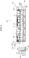
- Fig. 4 is a schematic view illustrating the configurations of the stage 10 and the LED controller 211 and illustrates a cross section of the stage 10.
- Fig. 5 is a schematic plan view illustrating a configuration of the light irradiation mechanism 140 to be described below.
- Fig. 6 is a view illustrating an example of a connection of the LEDs 141 in an LED unit U to be described below.
- Fig. 7 is a schematic view illustrating a configuration of a circuit for measuring a temperature of the electronic device D in the prober 1.
- the stage 10 is formed by stacking a plurality of functional parts including a top plate 120 as an uppermost plate part.
- the stage 10 is mounted on the moving mechanism 11 (see Fig. 2 ) for laterally and vertically moving the stage 10 through a heat insulating member (not shown).
- the heat insulating member is for thermally insulating the stage 10 from the moving mechanism 11.
- the stage 10 includes the top plate 120, a channel-forming member 130, and the light irradiation mechanism 140 as a heating mechanism in order from above.
- the top plate 120 is a member on which the wafer W is loaded.
- the top plate 120 is a member of which a surface 120a is a wafer loading surface as a substrate loading surface on which the wafer W is loaded.
- the surface 120a of the top plate 120 which is also an upper surface of the stage 10, will be referred to as the wafer loading surface 120a.
- the top plate 120 is formed, for example, in a disk shape.
- the top plate 120 is made of, for example, silicon carbide (SiC).
- SiC has characteristics of low specific heat and high thermal conductivity.
- SiC has a characteristic of high absorption efficiency of light emitted from the LEDs 141 of the light irradiation mechanism 140. Therefore, when the top plate 120 is made of SiC, the top plate 120 can be efficiently heated with light emitted from the light irradiation mechanism 140 or can be efficiently cooled with a refrigerant flowing in the refrigerant channels R, and thus, the wafer W loaded on the top plate 120 can be efficiently heated or cooled.
- Suction holes (not shown) for adsorbing the wafer W are formed in the wafer loading surface 120a of the top plate 120.
- a plurality of temperature sensors 121 are embedded in the top plate 120 at positions spaced apart from each other in a plan view.
- the channel-forming member 130 is a member which is bonded to a rear surface of the top plate 120 so as to be interposed between the top plate 120 and the light irradiation mechanism 140 and forms the refrigerant channels R in which a refrigerant flows between the light irradiation mechanism 140 and the top plate 120.
- the channel-forming member 130 is formed in a disk shape having substantially the same diameter as the top plate 120.
- a material of the channel-forming member 130 a material (for example, glass) capable of transmitting light (specifically, light emitted from the LEDs 141 to be described below) is used.
- Grooves are formed in a rear surface 120b of the top plate 120 on which the channel-forming member 130 is mounted, and the grooves are covered with the channel-forming member 130 to form the refrigerant channels R.
- the top plate 120 is cooled by a refrigerant flowing in the refrigerant channels R, thereby cooling the wafer W loaded on the top plate 120, that is, on the stage 10, and specifically, cooling the electronic device formed on the wafer W.
- a supply port 122 and a discharge port 123 communicating with the refrigerant channel R are formed in the top plate 120.
- a supply pipe 160 for supplying a refrigerant to the refrigerant channel R is connected to the supply port 122, and a discharge pipe 161 for discharging the refrigerant from the refrigerant channel R is connected to the discharge port 123.
- the supply pipe 160 is provided with a flow rate adjustment valve 162 which adjusts a flow rate of a refrigerant supplied to the refrigerant channel R, a chiller unit (not shown) which stores a refrigerant and adjusts a temperature of the refrigerant, and a pump (not shown).
- a material capable of transmitting light (specifically, light emitted from the LEDs 141 to be described below) is used and is supplied to the refrigerant channel R through the supply pipe 160 by the pump.
- a refrigerant having a temperature corresponding to a test temperature or a target temperature of the electronic device D is supplied to the refrigerant channel R.
- the temperature of the refrigerant is adjusted by the above-described chiller unit under control of the cooling controller 212 of the temperature controller 210.
- An operation of the flow rate adjustment valve 162 or the like for adjusting the flow rate of the refrigerant is controlled by the cooling controller 212 of the temperature controller 210.
- the light irradiation mechanism 140 includes the plurality of LEDs 141 as light-emitting elements facing the wafer W and heats the wafer W with light emitted from the LEDs 141.
- the light irradiation mechanism 140 is disposed to face the wafer W loaded on the wafer loading surface 120a of the top plate 120 through the channel-forming member 130.
- the light irradiation mechanism 140 includes a plurality of LED units U, in which the plurality of LEDs 141 are unitized, and at the same time, includes a base 142 on which the LED units U are mounted.
- the LED units U in the light irradiation mechanism 140 include planar square-shaped units U1 arranged in the same manner and in the same number as the electronic devices D (see Fig. 3 ) formed on the wafer W and planar non-square-shaped units U2 covering an outer circumference of the planar square-shaped units U1.
- the units U1 and the units U2 cover approximately the entire surface of the base 142.
- light emitted from the LEDs 141 of the LED units U may be emitted onto the entirety of a portion of the top plate 120, on which the wafer W is loaded, at least.
- Each LED 141 emits light (for example, infrared light) toward the wafer W.
- the light emitted from the LED 141 (hereinafter, in some cases, abbreviated as "LED light") passes through the channel-forming member 130 of the stage 10, which is made of a light-transmitting member.
- the light passing through the channel-forming member 130 passes through a refrigerant capable of transmitting light, which flows in the refrigerant channel R of the stage 10, and is incident on and absorbed by the top plate 120.
- the base 142 is formed in a disk shape having substantially the same diameter as the top plate 120. Furthermore, as shown in Fig. 4 , the base 142 has a concave portion 142a formed on a surface thereof, and the LED 141 is mounted in the concave portion 142a.
- the concave portion 142a may be filled with a material capable of transmitting LED light.
- the base 142 has a cooling water channel 142b, through which cooling water as a refrigerant for cooling the LED 141 flows, in a portion closer to a rear surface of the base 142.
- the base 142 is made of a metal material such as aluminum (Al).
- the light irradiation mechanism 140 LED light, which is incident on the top plate 120 on which the wafer W is loaded, is controlled in units of the LED unit U.
- the light irradiation mechanism 140 can emit the LED light only onto an arbitrary portion on the top plate 120 and can make the intensity of light emitted onto the arbitrary portion different from the intensity of light emitted onto another portion. Therefore, the light irradiation mechanism 140 can locally heat the wafer W loaded on the top plate 120 or may locally change the degree to which the wafer W is heated.
- the LED light is controlled in units of the LED unit U by the LED controller 211.
- each LED unit U is provided with a voltage measurement circuit M as a voltage measurement unit for measuring a voltage of the LED 141.
- the voltage measurement circuit M measures, for example, a voltage of one specific LED 141 in the LED unit U.
- one specific LED 141 of which a voltage is measured by the voltage measurement circuit M may be referred to as a representative LED 141.
- a measurement result by the voltage measurement circuit M is output to the main controller 200.
- a temperature of the electronic device D to be tested formed on the wafer W on the stage 10 is controlled to be constant at a target temperature through the heating by light emitted from the light irradiation mechanism 140 and through the heat absorption by a refrigerant flowing in the refrigerant channel R.
- the prober 1 measures the temperature of the electronic device D.
- the probes 12a are connected to the tester 4 through a plurality of wires 19 disposed at the interface 13.
- a relay 20 is provided in each of the two wires 19 connecting the tester 4 and two probes 12a in contact with two electrodes E of the potential difference generation circuit (for example, a diode) in the electronic device D.
- Each relay 20 may be configured to switch between the tester 4 and the potential difference measurement unit 14 to transmit a potential of each electrode E thereto. For example, when the electrical characteristics of the electronic device D are tested, after a voltage is applied when each relay 20 is mounted on each electrode E, each relay 20 transmits the potential of each electrode E to the potential difference measurement unit 14 at a predetermined timing.
- a potential difference generated when a current flows differs according to temperature. Therefore, the temperature of the electronic device D can be measured in real time during a test based on a potential difference of the potential difference generation circuit of the electronic device D, that is, a potential difference between the two electrodes E (probes 12a) of the potential difference generation circuit.
- the potential difference measurement unit 14 acquires the potential difference of the potential difference generation circuit of the electronic device D based on the potential of each electrode E transmitted through each relay 21. In addition, the potential difference measurement unit 14 transmits the acquired potential difference to the controller 16.
- the main controller 200 or the temperature controller 210 of the controller 16 calculates, i.e., measures, the temperature of the electronic device D based on the transmitted potential difference and the temperature characteristics of the potential difference of the potential difference generation circuit.
- a method of measuring the temperature of the electronic device D is not limited to the above-described method, and other methods may be used as long as the temperature of the electronic device D may be measured.
- the top plate 120 is cooled with a refrigerant having a temperature corresponding to a test temperature (or a target temperature) under control of the cooling controller 212.
- the LED controller 211 controls power (specifically, a current thereof) supplied to the LED 141 and controls the emission intensity of the LED 141 such that the temperature of the electronic device D becomes the test temperature (or the target temperature).
- the LED controller 211 includes a power supply unit 211a, a current adjustment circuit 211b, and a processing unit 211c.
- the power supply unit 211a outputs direct current (DC) power supplied to the LED 141.
- the current adjustment circuit 211b adjusts a current of the DC power supplied to each LED 141.
- the current adjustment circuit 211b for example, adjusts the current of the DC power supplied to each LED 141 in units of the LED unit U.
- the processing unit 211c is composed of, for example, a computer including a CPU, a memory, or the like and includes a program storage unit (not shown).
- the program storage unit stores programs that control the power supply unit 211a and the current adjustment circuit 211b.
- the program may be recorded on a computer-readable storage medium and may be installed in the processing unit 211c from the storage medium. Some or all of the programs may also be realized as dedicated hardware (circuit board).
- the LED controller 211 controls power supplied to the LED 141 corresponding to the electronic device D within a range, in which a current of the power does not exceed the allowable current Imax, such that the temperature of the electronic device D becomes a target temperature.
- the processing unit 211c determines a current of DC power supplied to the LED 141 corresponding to the electronic device D in a range, in which the current does not exceed the allowable current Imax, such that the temperature of the electronic device D becomes the target temperature.
- the current adjustment circuit 211b adjusts a current of DC power, which is supplied to the LED 141 corresponding to the electronic device D to be tested, so as to be become a current determined by the processing unit 211c.
- the allowable current Imax is preset based on a light output result when power is actually supplied to the corresponding LED 141.
- the allowable current Imax is corrected according to a state of the LED 141. Setting and correcting methods of the allowable current Imax will be described below.
- the wafer W is taken out of the FOUP of the loader 3, transferred toward the stage 10, and loaded on the wafer loading surface 120a of the top plate 120. Subsequently, the stage 10 is moved to a predetermined position.
- the stage 10 is moved, and each probe 12a provided above the stage 10 is brought into contact with the electrode E of the electronic device D to be tested of the wafer W.
- the potential difference measurement unit 14 acquires a potential difference of the above-described potential difference generation circuit in the electronic device D to be tested. Assuming that the temperature of the top plate 120 having the uniform temperature distribution at the surface thereof substantially matches a temperature of the electronic device D to be tested, the potential difference is calibrated, that is, information about temperature characteristics of the potential difference is corrected.
- the temperature of the electronic device D is measured.
- the LED controller 211 controls DC power supplied to the LED 141 corresponding to the electronic device D within a range, in which a current thereof does not exceed the allowable current Imax, such that the temperature of the electronic device D becomes a test temperature or a target temperature.
- a temperature and flow rate of a refrigerant in the refrigerant channel R are maintained constant, for example, at a value corresponding to the test temperature or the target temperature of the electronic device D to be tested.
- the wafer W is returned to the FOUP of the loader 3, a next wafer W is transferred to the stage 10, and then, the above-described processes are performed until a test of all the wafers W is completed.
- the allowable current Imax is preset for each LED 141 and then corrected for each LED 141. Specifically, the allowable current Imax is preset for each LED unit U and then corrected for each LED unit U.
- Fig. 8 is a functional block diagram of the main controller 200 relating to the setting and correcting of the allowable current Imax of the DC power supplied to the LED 141.
- Fig. 9 is a graph showing a relationship between a current of DC power supplied to the LED unit U and light output (intensity) of the LED unit U.
- the main controller 200 functions as an acquisition unit 201, a setting unit 202, and a correction unit 203 when a processor such as a CPU reads and executes a program stored in the program storage unit.
- the acquisition unit 201 supplies DC power to the LED 141 that is a setting target of the allowable current Imax in advance and actually causes the LED 141 to emit light to acquire a current-light output characteristic of the LED 141.
- the acquisition unit 201 controls the LED controller 211, supplies DC power to the LED unit U that is a setting target of the allowable current Imax, and actually causes the LED unit U to emit light to acquire a current-light output characteristic of the LED unit U as shown in Fig. 9 .
- the light output of the LED unit U is related to a temperature of a portion of the top plate 120 which is heated by LED light emitted from the LED unit U. Therefore, the acquisition unit 201 calculates and acquires the light output of the LED unit U from a measurement result by the temperature sensor 121 of the corresponding top plate 120 and information on a correlation between a temperature of the top plate 120 and intensity of light output, which is stored in a storage unit (not shown).
- the setting unit 202 Upon startup of the device or the like, the setting unit 202 presets the allowable current Imax for the LED 141 based on the current-light output characteristic, which is acquired by the acquisition unit 201, of the LED 141 that is the setting target of the allowable current Imax. In this case, the setting unit 202 sets the allowable current Imax from a current range in which light output is linearly changed with respect to a current in the acquired current-light output characteristic of the LED 141.
- the setting unit 202 sets the allowable current Imax for the LED unit U based on the current-light output characteristic, which is acquired by the acquisition unit 201, of the LED unit U that is the setting target of the allowable current Imax.
- the setting unit 202 sets the allowable current Imax from a current range B (see Fig. 9 ) in which light output is linearly changed with respect to a current in the acquired current-light output characteristic of the LED unit U.
- the setting unit 202 determines, for example, the maximum current included in the current range B as the allowable current Imax.
- the LED 141 can be driven efficiently, and even when the DC power is supplied to the LED 141, thermal runaway does not occur in the LED 141.
- the correction unit 203 corrects the allowable current Imax for the LED 141, which is a correction target of the allowable current Imax, according to a state of the LED 141.
- the correction unit 203 supplies the allowable current Imax to the LED 141, which is the correction target, in order to determine the state thereof, and then supplies an estimation current Ie to the LED 141. Furthermore, based on a result of measuring a voltage of the LED 141 at that time, the correction unit 203 estimates a junction temperature Tjm of the LED 141 when the allowable current Imax is supplied.
- a current I flowing in the LED 141 is represented by Equation 1 below using a voltage V applied to the LED 141 when DC power with the current I is supplied.
- I I s e qV / nkTj ⁇ 1
- Equation 2 nkTj / q lnI ⁇ lnI s
- the correction unit 203 supplies the DC powers with the currents I1 and I2 to the LED 141 at the known junction temperature Tj (for example, room temperature) in advance. Based on results of measuring the voltage V1 of the LED 141 at the current I1 and the voltage V2 of the LED 141 at the current 12, the correction unit 203 calculates the ideal factor n using Equation 4.
- the correction unit 203 supplies the DC power with the allowable current Imax to the LED 141, which is the correction target, in order to determine a state thereof, and then supplies the DC powers with the currents I1 and I2 as the estimation current Ie to the LED 141.
- the correction unit 203 uses Equation 5 to calculate, that is, estimate the junction temperature Tjm of the LED 141, which is the correction target, when the DC power with the allowable current Imax is supplied.
- the DC power with the allowable current Imax for determining the state is supplied for a predetermined time for which the junction temperature Tj is stabilized (estimated to be stabilized). Meanwhile, the time for which DC power with the estimation current Ie is supplied or DC power for calculating the ideal factor n is supplied is shorter than the above-described predetermined time.
- the junction temperature Tjm which is estimated for the LED 141 that is the correction target
- the allowable current Imax when the allowable current Imax is supplied, exceeds an allowable junction temperature Tmax corresponding to the allowable current Imax
- the following is estimated. That is, it is estimated that the LED 141 that is the correction target may be degraded such that luminous efficiency is lowered, and when the DC power with the allowable current Imax is supplied to the LED 141, thermal runaway may occur in the LED 141.
- the correction unit 203 corrects the allowable current Imax. For example, for the LED 141 that is the correction target, based on a difference between the estimated junction temperature Tjm and the allowable junction temperature Tmax, the correction unit 203 corrects the allowable current Imax such that the allowable current Imax is decreased.
- the correction unit 203 corrects the allowable current Imax for the LED unit U, which is a correction target of the allowable current Imax, according to a state of the LED unit U.
- the correction unit 203 controls the LED controller 211, supplies the power with the allowable current Imax to the LED unit U, which is the correction target, in order to determine a state thereof, and then supplies the DC power with the estimation current Ie to the LED unit U.
- the correction unit 203 estimates the junction temperature Tjm of the LED 141 when the allowable current Imax is supplied.
- the correction unit 203 controls the LED controller 211 at a known junction temperature Tj (for example, room temperature) in advance and supplies the DC powers with the currents I1 and I2 to the LED unit U that is the correction target. Based on results of measuring the voltage V1 of the LED 141 at the current I1 and the voltage V2 of the LED 141 at the current I2 in the LED unit U that is the correction target, the correction unit 203 calculates the ideal factor n using Equation 4.
- the correction unit 203 controls the LED controller 211, supplies the DC power with the allowable current Imax to the LED unit U, which is the correction target, in order to determine a state thereof, and then supplies the DC powers with the currents I1 and I2 as the estimation current Ie to the LED unit U141.
- the correction unit 203 calculates the following using Equation 5. That is, the correction unit 203 calculates, that is, estimates the junction temperature Tjm of the LED 141 when the DC power with the allowable current Imax is supplied.
- the correction unit 203 corrects the allowable current Imax. For example, for the LED unit U that is the correction target, based on a difference between the estimated junction temperature Tjm and the allowable junction temperature Tmax, the correction unit 203 corrects the allowable current Imax such that the allowable current Imax is decreased.
- Fig. 10 is a flowchart illustrating an example of the present correcting method.
- the present correcting method includes, before a process of correcting an allowable current Imax (operation S2), a preparation process of determining the allowable current Imax (initial value) or the like (operation S1).
- an acquisition unit 201 acquires a current-light output characteristic of each LED unit U (operation S11).
- the acquisition unit 201 performs the following processes on each LED unit U. That is, the acquisition unit 201 controls an LED controller 211, supplies each of a plurality of DC powers with different currents to each LED unit U, and cause the one LED unit U to emit light for a predetermined time to heat a top plate 120 until a temperature is stabilized. In addition, the acquisition unit 201 acquires a result of measuring a temperature of the top plate 120 by a temperature sensor 121 corresponding to the one LED unit U for each current (value) of the DC power supplied to the one LED unit U.
- the acquisition unit 201 acquires the current-light output characteristic of the one LED unit U from the result of measuring the temperature of the top plate 120 acquired for each current of the DC power and information on a correlation between a temperature of the top plate 120 and light output, which is stored in a storage unit (not shown).
- a setting unit 202 sets the allowable current Imax of an LED 141 for each LED unit U (operation S12).
- the setting unit 202 performs the following processes on each LED unit U. That is, the setting unit 202 extracts a current range B in which light output is linearly changed with respect to a current in the current-light output characteristic acquired in operation S11 for one LED unit U. The setting unit 202 determines the maximum current included in the current range B as the allowable current Imax (initial value) for the one LED unit U.
- a correction unit 203 calculates an ideal factor n for each LED unit U for correcting the allowable current Imax (operation S13).
- the correction unit 203 performs the following processes on each LED unit. That is, the correction unit 203 controls the LED controller 211 and supplies each of DC powers with currents I1 and I2 having two magnitudes to the one LED unit U for a short time in a state in which a junction temperature Tj of a representative LED 141 of the one LED unit U is stabilized at room temperature.
- the "short time” is a time (for example, several hundred microseconds) for which the junction temperature Tj of the representative LED 141 is not changed due to the supply of DC power.
- the correction unit 203 calculates the ideal factor n using Equation 4.
- the correction unit 203 acquires a relational equation between a junction temperature and a current in the LED 141 for correcting the allowable current Imax (operation S14).
- the correction unit 203 performs the following processes on each LED unit. That is, the correction unit 203 controls the LED controller 211 and supplies DC power with an equation acquisition current Ig to one LED unit U for a predetermined time (for example, several seconds) to stabilize the junction temperature Tj of the representative LED 141. Next, the correction unit 203 controls the LED controller 211 and stops the supply of the DC power with the equation acquisition current Ig to the one LED unit U, and then supplies each of the DC powers with the currents I1 and I2 as an estimation current Ie for a short time (for example, several hundred microseconds) before the junction temperature Tj of the representative LED 141 is decreased.
- a short time for example, several hundred microseconds
- the correction unit 203 calculate, using Equation 5, the junction temperature Tj of the representative LED 141 when the equation acquisition current Ig is supplied.
- the correction unit 203 acquires a relational equation between the junction temperature Tj and a current I in the representative LED 141 for one LED unit U.
- the above relational equation is represented by, for example, Equation 6 below.
- the correction unit 203 acquires an allowable junction temperature Tmax corresponding to the allowable current Imax of the LED 141 for correcting the allowable current Imax (operation S15).
- the correction unit 203 acquires the allowable junction temperature Tmax of the representative LED 141.
- the allowable current Imax may be actually supplied to each LED unit U, and a result of estimating the junction temperature Tj at that time may be used as the allowable junction temperature Tmax.
- a correction process of operation S2 is performed, for example, during idling (specifically, during replacement or maintenance of a wafer W).
- the correction process of operation S2 may be performed on each electronic device D to be tested or may be performed during a test of the electrical characteristics of one electronic device D.
- the correction unit 203 supplies DC power with the allowable current Imax for correction and estimates a junction temperature Tjm of the LED 141 of the LED unit U, which is a correction target, at that time (operation S21).
- the correction unit 203 controls the LED controller 211, supplies the DC power with the allowable current Imax to the LED unit U, which is the correction target, for a predetermined time (for example, several seconds), and stabilizes the junction temperature Tjm of the representative LED 141.
- the correction unit 203 controls the LED controller 211, stops the supply of the DC power with the allowable current Imax to the one LED unit U, which is the correction target, and then supplies each of the DC powers with the currents I1 and I2 as the estimation current Ie for a short time (for example, several hundred microseconds) before the junction temperature Tjm of the representative LED 141 is decreased.
- the correction unit 203 uses Equation 5 above to calculate, that is, estimate the junction temperature Tjm of the representative LED 141 when the DC power with the allowable current Imax is supplied.
- the correction unit 203 determines whether the junction temperature Tjm estimated in operation S21 exceeds the allowable junction temperature Tmax acquired in operation S15 (operation S22).
- the allowable current Imax (initial value) for the LED 141 is set from the current range B in which the light output is linearly changed with respect to the current in the previously acquired current-light output characteristic of the LED 141. Therefore, according to the present embodiment, the initial value of the allowable current Imax for the LED 141 can be maximized as much as possible within a range in which thermal runaway does not occur in the LED 141. That is, the performance of the LED 141 can be maximized.
- the junction temperature Tjm of the LED 41 when the allowable current Imax is supplied is estimated based on a result of measuring a voltage of the LED 141 when DC power with the estimation current Ie is supplied after DC power with the allowable current Imax is supplied to the LED 141 for correction.
- the estimated junction temperature Tjm exceeds the allowable junction temperature Tmax corresponding to the allowable current Imax, that is, when a state of the LED 141 to be corrected is changed and there is a fear that degradation or the like may occur, the allowable current Imax is corrected. Therefore, according to the present embodiment, it is possible to prevent thermal runaway from occurring in the LED 141 when degradation or the like occurs in the LED 141.
- the utilization efficiency of the LED 141 can be improved over a long period of time.
- the acquisition unit 201 actually supplies DC power to the LED 141 in a prober 1, causes the LED 141 to emit light, and acquires the current-light output characteristic of the LED 141.
- DC power may be supplied to the LED 141 outside the prober 1 to acquire the current-light output characteristic of the LED 141.
- the setting unit 202 sets the allowable current Imax based on the current-light output characteristic of the LED 141.
- the current-light output characteristic of the LED 141 may be displayed on a display unit of a user interface unit 18, and the allowable current Imax may be set based on an input of a user of the prober 1 who sees the displayed content.
- the number of representative LEDs 141 that is, the number of LEDs 141 provided with the voltage measurement circuit M is one but may be plural.
- the correction unit 203 estimates the junction temperature Tjm of the LED 141 when the allowable current Imax is supplied. As a result, it is possible to reduce a variation between the individual LEDs 141 when estimating the junction temperature Tjm or the like.
- the voltage measurement circuit M measures a voltage between an anode and a cathode of a single LED 141.
- the present disclosure is not limited thereto, and the voltage measurement circuit M may combine voltages between an anode and a cathode of an LED set in which a plurality of LEDs 141 are connected in series.
- the correction unit 203 estimates the junction temperature Tjm of the LED 141 when the allowable current Imax is supplied. Even in this case, it is possible to absorb a variation between the individual LEDs 141 when estimating the junction temperature Tjm or the like.
- the plurality of LEDs 141 are included in each LED unit U, but one LED 141 may be included.
- a heating device in addition to a prober, can be applied to a system as long as the system adjusts a temperature of a heating target with light emitted from the LED 141.
Landscapes
- Engineering & Computer Science (AREA)
- General Physics & Mathematics (AREA)
- Physics & Mathematics (AREA)
- Environmental & Geological Engineering (AREA)
- Toxicology (AREA)
- Health & Medical Sciences (AREA)
- Manufacturing & Machinery (AREA)
- Computer Hardware Design (AREA)
- Microelectronics & Electronic Packaging (AREA)
- General Engineering & Computer Science (AREA)
- Testing Of Individual Semiconductor Devices (AREA)
- Testing Or Measuring Of Semiconductors Or The Like (AREA)
- Led Devices (AREA)
Applications Claiming Priority (1)
| Application Number | Priority Date | Filing Date | Title |
|---|---|---|---|
| JP2020205999A JP7581034B2 (ja) | 2020-12-11 | 2020-12-11 | 加熱装置及びledの制御方法 |
Publications (3)
| Publication Number | Publication Date |
|---|---|
| EP4012425A2 true EP4012425A2 (de) | 2022-06-15 |
| EP4012425A3 EP4012425A3 (de) | 2022-06-22 |
| EP4012425B1 EP4012425B1 (de) | 2024-08-21 |
Family
ID=78822342
Family Applications (1)
| Application Number | Title | Priority Date | Filing Date |
|---|---|---|---|
| EP21212788.0A Active EP4012425B1 (de) | 2020-12-11 | 2021-12-07 | Heizvorrichtung und verfahren zur led-steuerung |
Country Status (6)
| Country | Link |
|---|---|
| US (1) | US12557182B2 (de) |
| EP (1) | EP4012425B1 (de) |
| JP (1) | JP7581034B2 (de) |
| KR (1) | KR102660269B1 (de) |
| CN (1) | CN114630454B (de) |
| TW (1) | TWI888679B (de) |
Cited By (1)
| Publication number | Priority date | Publication date | Assignee | Title |
|---|---|---|---|---|
| TWI919866B (zh) | 2024-04-26 | 2026-03-21 | 南韓商Hs高科技股份有限公司 | 發光二極體(led)加熱器系統以及配備所述加熱器系統的半導體晶圓處理裝置 |
Families Citing this family (1)
| Publication number | Priority date | Publication date | Assignee | Title |
|---|---|---|---|---|
| JP2024111585A (ja) * | 2023-02-06 | 2024-08-19 | 株式会社デンソー | 光学センサ |
Citations (1)
| Publication number | Priority date | Publication date | Assignee | Title |
|---|---|---|---|---|
| JP2019102645A (ja) | 2017-12-01 | 2019-06-24 | 東京エレクトロン株式会社 | プローバ |
Family Cites Families (17)
| Publication number | Priority date | Publication date | Assignee | Title |
|---|---|---|---|---|
| JP2005115350A (ja) * | 2003-09-17 | 2005-04-28 | Seiko Epson Corp | 温度測定装置、光源制御装置、プロジェクタ、温度測定方法および光源制御方法 |
| JP3984214B2 (ja) * | 2003-10-21 | 2007-10-03 | ローム株式会社 | 発光制御装置 |
| JP2006066498A (ja) * | 2004-08-25 | 2006-03-09 | Seiko Epson Corp | 温度測定装置、光源制御装置、画像表示装置、温度測定方法および光源制御方法 |
| JP2007042839A (ja) * | 2005-08-03 | 2007-02-15 | Shinko Electric Ind Co Ltd | レーザ光源の駆動回路および駆動方法 |
| JP2007109747A (ja) * | 2005-10-12 | 2007-04-26 | Stanley Electric Co Ltd | Led点灯制御装置 |
| JP2008124303A (ja) * | 2006-11-14 | 2008-05-29 | Seiko Epson Corp | 半導体発光素子の駆動制御装置、駆動制御装置を有する投写表示装置、および、それらの方法 |
| EP2245904A2 (de) * | 2008-01-28 | 2010-11-03 | Nxp B.V. | System und verfahren zur schätzung der sperrschichttemperatur einer lichtemittierenden diode |
| JP2009253242A (ja) * | 2008-04-11 | 2009-10-29 | Tokyo Electron Ltd | アニール装置 |
| WO2010049882A2 (en) * | 2008-10-30 | 2010-05-06 | Nxp B.V. | Lighting unit with temperature protection |
| US9326346B2 (en) * | 2009-01-13 | 2016-04-26 | Terralux, Inc. | Method and device for remote sensing and control of LED lights |
| JP2013517613A (ja) * | 2009-11-17 | 2013-05-16 | テララックス, インコーポレイテッド | Led電源の検出および制御 |
| CN102693925B (zh) * | 2011-03-25 | 2016-05-25 | 夏普株式会社 | 半导体发光元件的温度特性检查装置和温度特性检查方法 |
| JP6267162B2 (ja) * | 2014-09-09 | 2018-01-24 | 東京エレクトロン株式会社 | 熱処理方法及び熱処理装置 |
| JP6800072B2 (ja) * | 2017-03-31 | 2020-12-16 | アズビル株式会社 | 劣化診断方法 |
| JP7042158B2 (ja) * | 2018-05-23 | 2022-03-25 | 東京エレクトロン株式会社 | 検査装置及び温度制御方法 |
| JP2020009927A (ja) * | 2018-07-09 | 2020-01-16 | フェニックス電機株式会社 | 加熱用ledランプ、およびそれを備えるウエハ加熱ユニット |
| JP7228111B2 (ja) * | 2018-10-02 | 2023-02-24 | 日亜化学工業株式会社 | 紫外線照射装置及び紫外線硬化樹脂の硬化方法 |
-
2020
- 2020-12-11 JP JP2020205999A patent/JP7581034B2/ja active Active
-
2021
- 2021-11-30 KR KR1020210167814A patent/KR102660269B1/ko active Active
- 2021-12-02 TW TW110144959A patent/TWI888679B/zh active
- 2021-12-03 CN CN202111469650.7A patent/CN114630454B/zh active Active
- 2021-12-06 US US17/543,012 patent/US12557182B2/en active Active
- 2021-12-07 EP EP21212788.0A patent/EP4012425B1/de active Active
Patent Citations (1)
| Publication number | Priority date | Publication date | Assignee | Title |
|---|---|---|---|---|
| JP2019102645A (ja) | 2017-12-01 | 2019-06-24 | 東京エレクトロン株式会社 | プローバ |
Cited By (1)
| Publication number | Priority date | Publication date | Assignee | Title |
|---|---|---|---|---|
| TWI919866B (zh) | 2024-04-26 | 2026-03-21 | 南韓商Hs高科技股份有限公司 | 發光二極體(led)加熱器系統以及配備所述加熱器系統的半導體晶圓處理裝置 |
Also Published As
| Publication number | Publication date |
|---|---|
| TW202224052A (zh) | 2022-06-16 |
| TWI888679B (zh) | 2025-07-01 |
| JP2022092972A (ja) | 2022-06-23 |
| US20220191974A1 (en) | 2022-06-16 |
| EP4012425B1 (de) | 2024-08-21 |
| KR20220083587A (ko) | 2022-06-20 |
| US12557182B2 (en) | 2026-02-17 |
| CN114630454A (zh) | 2022-06-14 |
| EP4012425A3 (de) | 2022-06-22 |
| JP7581034B2 (ja) | 2024-11-12 |
| KR102660269B1 (ko) | 2024-04-23 |
| CN114630454B (zh) | 2024-11-01 |
Similar Documents
| Publication | Publication Date | Title |
|---|---|---|
| EP3799111B1 (de) | Inspektionsvorrichtung und temperaturregelungsverfahren | |
| US11125813B2 (en) | Prober | |
| US7554350B2 (en) | Burn-in system with heating blocks accommodated in cooling blocks | |
| KR101344348B1 (ko) | 반도체 소자의 테스트 소켓 및 이를 이용한 반도체 소자의테스트 방법 | |
| EP3550313B1 (de) | Inspektionsvorrichtung für elektronische vorrichtung | |
| CN100533165C (zh) | 执行电子器件的晶片级老化的方法 | |
| US11221358B2 (en) | Placement stand and electronic device inspecting apparatus | |
| EP4012425B1 (de) | Heizvorrichtung und verfahren zur led-steuerung | |
| US7064568B2 (en) | Optical testing of integrated circuits with temperature control | |
| US7642795B2 (en) | Drive method and drive circuit of peltier element, attaching structure of peltier module and electronic device handling apparatus | |
| US20100013509A1 (en) | Prober and semiconductor wafer testing method using the same | |
| KR20250130649A (ko) | 검사 시스템 및 온도 제어 방법 | |
| JP2022071468A (ja) | 載置台、検査装置及び検査方法 | |
| EP1196790B1 (de) | Gerät und verfahren zur temperaturkontrolle von integrierten schaltungen während der prüfung | |
| US20020175694A1 (en) | Method of burning in an integrated circuit chip package | |
| KR100950701B1 (ko) | 메모리 모듈 실장 테스터용 가열장치 및 이를 이용한메모리 모듈 가열방법 | |
| JP7449814B2 (ja) | 検査方法及び検査装置 | |
| US8039277B2 (en) | Providing current control over wafer borne semiconductor devices using overlayer patterns |
Legal Events
| Date | Code | Title | Description |
|---|---|---|---|
| PUAI | Public reference made under article 153(3) epc to a published international application that has entered the european phase |
Free format text: ORIGINAL CODE: 0009012 |
|
| STAA | Information on the status of an ep patent application or granted ep patent |
Free format text: STATUS: REQUEST FOR EXAMINATION WAS MADE |
|
| PUAL | Search report despatched |
Free format text: ORIGINAL CODE: 0009013 |
|
| 17P | Request for examination filed |
Effective date: 20211207 |
|
| AK | Designated contracting states |
Kind code of ref document: A2 Designated state(s): AL AT BE BG CH CY CZ DE DK EE ES FI FR GB GR HR HU IE IS IT LI LT LU LV MC MK MT NL NO PL PT RO RS SE SI SK SM TR |
|
| AK | Designated contracting states |
Kind code of ref document: A3 Designated state(s): AL AT BE BG CH CY CZ DE DK EE ES FI FR GB GR HR HU IE IS IT LI LT LU LV MC MK MT NL NO PL PT RO RS SE SI SK SM TR |
|
| RIC1 | Information provided on ipc code assigned before grant |
Ipc: H05B 3/00 20060101ALI20220518BHEP Ipc: H05B 47/28 20200101ALI20220518BHEP Ipc: H05B 45/18 20200101ALI20220518BHEP Ipc: H01L 21/67 20060101ALI20220518BHEP Ipc: G01R 31/28 20060101AFI20220518BHEP |
|
| GRAP | Despatch of communication of intention to grant a patent |
Free format text: ORIGINAL CODE: EPIDOSNIGR1 |
|
| STAA | Information on the status of an ep patent application or granted ep patent |
Free format text: STATUS: GRANT OF PATENT IS INTENDED |
|
| INTG | Intention to grant announced |
Effective date: 20240314 |
|
| GRAS | Grant fee paid |
Free format text: ORIGINAL CODE: EPIDOSNIGR3 |
|
| GRAA | (expected) grant |
Free format text: ORIGINAL CODE: 0009210 |
|
| STAA | Information on the status of an ep patent application or granted ep patent |
Free format text: STATUS: THE PATENT HAS BEEN GRANTED |
|
| AK | Designated contracting states |
Kind code of ref document: B1 Designated state(s): AL AT BE BG CH CY CZ DE DK EE ES FI FR GB GR HR HU IE IS IT LI LT LU LV MC MK MT NL NO PL PT RO RS SE SI SK SM TR |
|
| REG | Reference to a national code |
Ref country code: GB Ref legal event code: FG4D |
|
| REG | Reference to a national code |
Ref country code: CH Ref legal event code: EP |
|
| REG | Reference to a national code |
Ref country code: DE Ref legal event code: R096 Ref document number: 602021017472 Country of ref document: DE |
|
| REG | Reference to a national code |
Ref country code: IE Ref legal event code: FG4D |
|
| REG | Reference to a national code |
Ref country code: LT Ref legal event code: MG9D |
|
| REG | Reference to a national code |
Ref country code: NL Ref legal event code: MP Effective date: 20240821 |
|
| PG25 | Lapsed in a contracting state [announced via postgrant information from national office to epo] |
Ref country code: NO Free format text: LAPSE BECAUSE OF FAILURE TO SUBMIT A TRANSLATION OF THE DESCRIPTION OR TO PAY THE FEE WITHIN THE PRESCRIBED TIME-LIMIT Effective date: 20241121 |
|
| REG | Reference to a national code |
Ref country code: AT Ref legal event code: MK05 Ref document number: 1715999 Country of ref document: AT Kind code of ref document: T Effective date: 20240821 |
|
| PG25 | Lapsed in a contracting state [announced via postgrant information from national office to epo] |
Ref country code: NL Free format text: LAPSE BECAUSE OF FAILURE TO SUBMIT A TRANSLATION OF THE DESCRIPTION OR TO PAY THE FEE WITHIN THE PRESCRIBED TIME-LIMIT Effective date: 20240821 Ref country code: FI Free format text: LAPSE BECAUSE OF FAILURE TO SUBMIT A TRANSLATION OF THE DESCRIPTION OR TO PAY THE FEE WITHIN THE PRESCRIBED TIME-LIMIT Effective date: 20240821 Ref country code: PT Free format text: LAPSE BECAUSE OF FAILURE TO SUBMIT A TRANSLATION OF THE DESCRIPTION OR TO PAY THE FEE WITHIN THE PRESCRIBED TIME-LIMIT Effective date: 20241223 Ref country code: PL Free format text: LAPSE BECAUSE OF FAILURE TO SUBMIT A TRANSLATION OF THE DESCRIPTION OR TO PAY THE FEE WITHIN THE PRESCRIBED TIME-LIMIT Effective date: 20240821 Ref country code: GR Free format text: LAPSE BECAUSE OF FAILURE TO SUBMIT A TRANSLATION OF THE DESCRIPTION OR TO PAY THE FEE WITHIN THE PRESCRIBED TIME-LIMIT Effective date: 20241122 |
|
| PG25 | Lapsed in a contracting state [announced via postgrant information from national office to epo] |
Ref country code: BG Free format text: LAPSE BECAUSE OF FAILURE TO SUBMIT A TRANSLATION OF THE DESCRIPTION OR TO PAY THE FEE WITHIN THE PRESCRIBED TIME-LIMIT Effective date: 20240821 |
|
| PG25 | Lapsed in a contracting state [announced via postgrant information from national office to epo] |
Ref country code: LV Free format text: LAPSE BECAUSE OF FAILURE TO SUBMIT A TRANSLATION OF THE DESCRIPTION OR TO PAY THE FEE WITHIN THE PRESCRIBED TIME-LIMIT Effective date: 20240821 |
|
| PG25 | Lapsed in a contracting state [announced via postgrant information from national office to epo] |
Ref country code: IS Free format text: LAPSE BECAUSE OF FAILURE TO SUBMIT A TRANSLATION OF THE DESCRIPTION OR TO PAY THE FEE WITHIN THE PRESCRIBED TIME-LIMIT Effective date: 20241221 Ref country code: AT Free format text: LAPSE BECAUSE OF FAILURE TO SUBMIT A TRANSLATION OF THE DESCRIPTION OR TO PAY THE FEE WITHIN THE PRESCRIBED TIME-LIMIT Effective date: 20240821 |
|
| PG25 | Lapsed in a contracting state [announced via postgrant information from national office to epo] |
Ref country code: HR Free format text: LAPSE BECAUSE OF FAILURE TO SUBMIT A TRANSLATION OF THE DESCRIPTION OR TO PAY THE FEE WITHIN THE PRESCRIBED TIME-LIMIT Effective date: 20240821 |
|
| PG25 | Lapsed in a contracting state [announced via postgrant information from national office to epo] |
Ref country code: ES Free format text: LAPSE BECAUSE OF FAILURE TO SUBMIT A TRANSLATION OF THE DESCRIPTION OR TO PAY THE FEE WITHIN THE PRESCRIBED TIME-LIMIT Effective date: 20240821 Ref country code: RS Free format text: LAPSE BECAUSE OF FAILURE TO SUBMIT A TRANSLATION OF THE DESCRIPTION OR TO PAY THE FEE WITHIN THE PRESCRIBED TIME-LIMIT Effective date: 20241121 |
|
| PG25 | Lapsed in a contracting state [announced via postgrant information from national office to epo] |
Ref country code: RS Free format text: LAPSE BECAUSE OF FAILURE TO SUBMIT A TRANSLATION OF THE DESCRIPTION OR TO PAY THE FEE WITHIN THE PRESCRIBED TIME-LIMIT Effective date: 20241121 Ref country code: PT Free format text: LAPSE BECAUSE OF FAILURE TO SUBMIT A TRANSLATION OF THE DESCRIPTION OR TO PAY THE FEE WITHIN THE PRESCRIBED TIME-LIMIT Effective date: 20241223 Ref country code: PL Free format text: LAPSE BECAUSE OF FAILURE TO SUBMIT A TRANSLATION OF THE DESCRIPTION OR TO PAY THE FEE WITHIN THE PRESCRIBED TIME-LIMIT Effective date: 20240821 Ref country code: NO Free format text: LAPSE BECAUSE OF FAILURE TO SUBMIT A TRANSLATION OF THE DESCRIPTION OR TO PAY THE FEE WITHIN THE PRESCRIBED TIME-LIMIT Effective date: 20241121 Ref country code: NL Free format text: LAPSE BECAUSE OF FAILURE TO SUBMIT A TRANSLATION OF THE DESCRIPTION OR TO PAY THE FEE WITHIN THE PRESCRIBED TIME-LIMIT Effective date: 20240821 Ref country code: LV Free format text: LAPSE BECAUSE OF FAILURE TO SUBMIT A TRANSLATION OF THE DESCRIPTION OR TO PAY THE FEE WITHIN THE PRESCRIBED TIME-LIMIT Effective date: 20240821 Ref country code: IS Free format text: LAPSE BECAUSE OF FAILURE TO SUBMIT A TRANSLATION OF THE DESCRIPTION OR TO PAY THE FEE WITHIN THE PRESCRIBED TIME-LIMIT Effective date: 20241221 Ref country code: HR Free format text: LAPSE BECAUSE OF FAILURE TO SUBMIT A TRANSLATION OF THE DESCRIPTION OR TO PAY THE FEE WITHIN THE PRESCRIBED TIME-LIMIT Effective date: 20240821 Ref country code: GR Free format text: LAPSE BECAUSE OF FAILURE TO SUBMIT A TRANSLATION OF THE DESCRIPTION OR TO PAY THE FEE WITHIN THE PRESCRIBED TIME-LIMIT Effective date: 20241122 Ref country code: FI Free format text: LAPSE BECAUSE OF FAILURE TO SUBMIT A TRANSLATION OF THE DESCRIPTION OR TO PAY THE FEE WITHIN THE PRESCRIBED TIME-LIMIT Effective date: 20240821 Ref country code: ES Free format text: LAPSE BECAUSE OF FAILURE TO SUBMIT A TRANSLATION OF THE DESCRIPTION OR TO PAY THE FEE WITHIN THE PRESCRIBED TIME-LIMIT Effective date: 20240821 Ref country code: BG Free format text: LAPSE BECAUSE OF FAILURE TO SUBMIT A TRANSLATION OF THE DESCRIPTION OR TO PAY THE FEE WITHIN THE PRESCRIBED TIME-LIMIT Effective date: 20240821 Ref country code: AT Free format text: LAPSE BECAUSE OF FAILURE TO SUBMIT A TRANSLATION OF THE DESCRIPTION OR TO PAY THE FEE WITHIN THE PRESCRIBED TIME-LIMIT Effective date: 20240821 |
|
| PG25 | Lapsed in a contracting state [announced via postgrant information from national office to epo] |
Ref country code: RO Free format text: LAPSE BECAUSE OF FAILURE TO SUBMIT A TRANSLATION OF THE DESCRIPTION OR TO PAY THE FEE WITHIN THE PRESCRIBED TIME-LIMIT Effective date: 20240821 Ref country code: DK Free format text: LAPSE BECAUSE OF FAILURE TO SUBMIT A TRANSLATION OF THE DESCRIPTION OR TO PAY THE FEE WITHIN THE PRESCRIBED TIME-LIMIT Effective date: 20240821 Ref country code: SM Free format text: LAPSE BECAUSE OF FAILURE TO SUBMIT A TRANSLATION OF THE DESCRIPTION OR TO PAY THE FEE WITHIN THE PRESCRIBED TIME-LIMIT Effective date: 20240821 |
|
| PG25 | Lapsed in a contracting state [announced via postgrant information from national office to epo] |
Ref country code: EE Free format text: LAPSE BECAUSE OF FAILURE TO SUBMIT A TRANSLATION OF THE DESCRIPTION OR TO PAY THE FEE WITHIN THE PRESCRIBED TIME-LIMIT Effective date: 20240821 |
|
| PG25 | Lapsed in a contracting state [announced via postgrant information from national office to epo] |
Ref country code: CZ Free format text: LAPSE BECAUSE OF FAILURE TO SUBMIT A TRANSLATION OF THE DESCRIPTION OR TO PAY THE FEE WITHIN THE PRESCRIBED TIME-LIMIT Effective date: 20240821 |
|
| PG25 | Lapsed in a contracting state [announced via postgrant information from national office to epo] |
Ref country code: SK Free format text: LAPSE BECAUSE OF FAILURE TO SUBMIT A TRANSLATION OF THE DESCRIPTION OR TO PAY THE FEE WITHIN THE PRESCRIBED TIME-LIMIT Effective date: 20240821 Ref country code: IT Free format text: LAPSE BECAUSE OF FAILURE TO SUBMIT A TRANSLATION OF THE DESCRIPTION OR TO PAY THE FEE WITHIN THE PRESCRIBED TIME-LIMIT Effective date: 20240821 |
|
| REG | Reference to a national code |
Ref country code: DE Ref legal event code: R097 Ref document number: 602021017472 Country of ref document: DE |
|
| PLBE | No opposition filed within time limit |
Free format text: ORIGINAL CODE: 0009261 |
|
| STAA | Information on the status of an ep patent application or granted ep patent |
Free format text: STATUS: NO OPPOSITION FILED WITHIN TIME LIMIT |
|
| PG25 | Lapsed in a contracting state [announced via postgrant information from national office to epo] |
Ref country code: MC Free format text: LAPSE BECAUSE OF FAILURE TO SUBMIT A TRANSLATION OF THE DESCRIPTION OR TO PAY THE FEE WITHIN THE PRESCRIBED TIME-LIMIT Effective date: 20240821 |
|
| 26N | No opposition filed |
Effective date: 20250522 |
|
| REG | Reference to a national code |
Ref country code: CH Ref legal event code: PL |
|
| PG25 | Lapsed in a contracting state [announced via postgrant information from national office to epo] |
Ref country code: LU Free format text: LAPSE BECAUSE OF NON-PAYMENT OF DUE FEES Effective date: 20241207 |
|
| PG25 | Lapsed in a contracting state [announced via postgrant information from national office to epo] |
Ref country code: SE Free format text: LAPSE BECAUSE OF FAILURE TO SUBMIT A TRANSLATION OF THE DESCRIPTION OR TO PAY THE FEE WITHIN THE PRESCRIBED TIME-LIMIT Effective date: 20240821 |
|
| REG | Reference to a national code |
Ref country code: BE Ref legal event code: MM Effective date: 20241231 |
|
| PG25 | Lapsed in a contracting state [announced via postgrant information from national office to epo] |
Ref country code: BE Free format text: LAPSE BECAUSE OF NON-PAYMENT OF DUE FEES Effective date: 20241231 |
|
| PG25 | Lapsed in a contracting state [announced via postgrant information from national office to epo] |
Ref country code: FR Free format text: LAPSE BECAUSE OF NON-PAYMENT OF DUE FEES Effective date: 20241231 |
|
| PG25 | Lapsed in a contracting state [announced via postgrant information from national office to epo] |
Ref country code: CH Free format text: LAPSE BECAUSE OF NON-PAYMENT OF DUE FEES Effective date: 20241231 |
|
| PG25 | Lapsed in a contracting state [announced via postgrant information from national office to epo] |
Ref country code: IE Free format text: LAPSE BECAUSE OF NON-PAYMENT OF DUE FEES Effective date: 20241207 |
|
| PGFP | Annual fee paid to national office [announced via postgrant information from national office to epo] |
Ref country code: DE Payment date: 20251028 Year of fee payment: 5 |
|
| PG25 | Lapsed in a contracting state [announced via postgrant information from national office to epo] |
Ref country code: CY Free format text: LAPSE BECAUSE OF FAILURE TO SUBMIT A TRANSLATION OF THE DESCRIPTION OR TO PAY THE FEE WITHIN THE PRESCRIBED TIME-LIMIT; INVALID AB INITIO Effective date: 20211207 |